

Microchip Technology Inc PIC18F010-I-P, PIC18F010-I-SN, PIC18F020-I-P, PIC18F020-I-SN Datasheet

2001 Microchip Technology Inc. Preliminary DS41142A
PIC18F010/020
Data Sheet
High Performance Microcontrollers

DS41142A - page ii Preliminary 2001 Microchip Technology Inc.
“All rights reserved. Copyright © 2001, Microchip Technology
Incorporated, USA. Information contained in this publication
regarding device applications and the like is intended through
suggestion only and may be superseded by updates. No representation or warranty is given and no liability is assumed by
Microchip Technology Incorporated with respect to the accuracy or use of such information, or infringement of patents or
other intellectual property rights arising from such use or ot herwise. Use of Microchip’s products as critical components in
life support systems is not authorized except with express
written approval by Microchip. No licenses are conveyed,
implicitly or otherwise, under any intellectual property rights.
The Microchip logo and name are registered trademarks of
Microchip Technology Inc. in the U.S.A. and other countries.
All rights reserved. All other trademarks mentioned herein are
the property of their respective companies. No licenses are
conveyed, implicitly or otherwise, under any intellectual property rights.”
Trademarks
The Microchip name, logo, PIC, PICmicro, PICMASTER, PICSTART, PRO MATE, K
EELOQ, SEEVAL, MPLAB and The
Embedded Control Solutions Company are registered trademarks of Microchip Technology Incorporated in the U.S.A. and
other countries.
Total Endurance, ICSP, In-Circuit Serial Programming, FilterLab, MXDEV, microID, FlexROM, fuzzyLAB, MPASM,
MPLINK, MPLIB, PICDEM, ICEPIC, Migratable Memory,
FanSense, ECONOMONITOR and SelectMode are trademarks of Microchip Technology Incorporated in the U.S.A.
Serialized Quick T erm Programming (SQTP) is a service mark
of Microchip Technology Incorporated in the U.S.A.
All other trademarks mentioned herein are property of their
respective companies.
© 2001, Microchip Technology Incorporated, Printed in the
U.S.A., All Rights Reserved.
Microchip received QS-9000 quality system
certification for its worldwide headquarters,
design and wafer fabrication facilities in
Chandler and Tempe, Arizona in July 1999. The
Company’s quality system processes and
procedures are QS-9000 compliant for its
PICmicro
®
8-bit MCUs, KEELOQ
®
code hoppin g
devices, Serial EEPROMs and microperipheral
products. In addition, Microchip’s quality
system for the design and manufacture of
development systems is ISO 9001 certified.
2001 Microchip Technology Inc. Preliminary DS41142A-page 1
PIC18F010/020
High Performance RISC CPU:
• C compiler optimized instru ction set
• Linear program memory addressing
- 4096 x 8 on-chip FLASH program memory
- 2048 x 8 on-chip FLASH program memory
(PIC18F010)
• Linear data memory addressing
- 256 x 8 general purpose registers
- 64 x 8 EEPROM
• Operating speed:
- DC - 40MHz clock input
- DC - 100 ns instruction cycle
- Internal oscillator with 5 program
selectable speeds (32kHz, 500kHz, 1MHz,
4MHz, 8MHz)
• 2.0V operation (4MHz)
• 16-bit wide instructions
• 8-bit wide data path
• 31 levels of hardware stack
• Software stack capability
• Multi-vector interrupt capability
• 8 x 8 multiply single cycle hardware
Special Microcontroll er Features:
• Power-on Reset (POR), Power-up Timer (PWR T )
and Oscillator Start-up Timer (OST)
• Brown-out Reset (BOR)
• Programmable Low Voltage Detection circuitry
(PLVD)
• Watchdog Timer (WDT) with its own on-chip
RC oscillator for reliable operation
• Programmable code protection
• Power saving SLEEP mode with Wake-up on Pin
Change
• In-Circuit Serial Programming (ICSPTM) via two
pins
• Low cost MPLAB
®
ICD available
Peripheral Features:
• High current sink/source 25mA/25mA
• Timer0: 8-bit/16-bit timer/counter with 8-bit
programmable prescaler
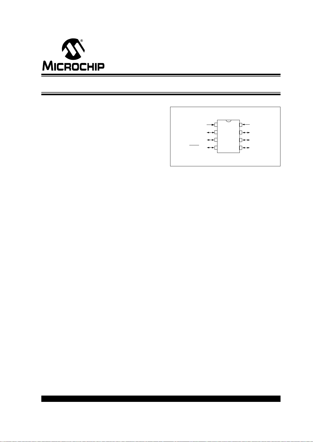
Pinout Diagram:
CMOS T echnology:
• Low power, high speed C MOS FLASH technology
• Fully static design
• Wide operating voltage range (2.0V to 5.5V)
• Commercial, Industrial and Extended
temperature ranges
• Low power consumption
PDIP, SOIC
8
7
6
5
1
2
3
4
VDD
RB5/OSC1/CLKIN
RB4/OSC2/CLKOUT
RB3/MCLR
/VPP
VSS
RB0/ICSPDAT
RB1/ICSPCLK
RB2/T0CKI/INT0
PIC18F010/020
High Performance Microcontr ollers

PIC18F010/020
DS41142A-page 2 Preliminary 2001 Microchip Technology Inc.
Table of Contents
1.0 Device Overview............................... ...... ..... ...... ....................................... ...... ...... ..... ........................................3
2.0 Oscillator Configurations....................................................................................................................................7
3.0 Reset................................................................................................................................................................15
4.0 Memory Organization.......................................................................................................................................23
5.0 Data EEPROM Memory...................................................................................................................................43
6.0 Table Read/Write Instructions..........................................................................................................................47
7.0 8 X 8 Hardware Multiplier.................................................................................................................................55
8.0 Interrupts..........................................................................................................................................................59
9.0 I/O Port.............................................................................................................................................................67
10.0 Timer0 Module.................................................................................................................................................73
11.0 Low Voltage Detect..........................................................................................................................................77
12.0 Special Features of the CPU............................................................................................................................83
13.0 Instruction Set Summary..................................................................................................................................95
14.0 Development Support.....................................................................................................................................139
15.0 Electrical Characteristics........................................................... .....................................................................145
16.0 DC and AC Characteristics Graphs and Tables.............................................................................................157
17.0 Packaging Information....................................................................................................................................159
Appendix A: Conversion Considerations ..................................................................................................................163
Appendix B: Migration from Baseline to Enhanced Devices.....................................................................................163
Appendix C: Migration from Mid-range to Enhanced Devices..................................................................................164
Appendix D: Migration from High-end to Enhanced Devices....................................................................................164
Index .......................................................................................................................................................................165
On-Line Support..........................................................................................................................................................169
Reader Response.......................................................................................................................................................170
PIC18F010/020 Product Identification System............................................................................................................171
TO OUR VALUED CUSTOMERS
It is our intention to provide our valued customers with the best documentation possible to ensure successful use of your Microchip
products. To this end, we will continue to improve our publications to better suit your needs. Our publications will be refined and
enhanced as new volumes and updates are introduced.
If you have any questions or co mm ents regarding this publication, please contact the Marketing Communications Department via
E-mail at docerrors@mail.microchip.com or fax the Reader Response Form in the back of this data sheet to (480) 792-4150.
We welcome your feedback.
Most Current Data Sheet
To obtain the most up-to-date version of this data sheet, please register at our Worldwide Web site at:
http://www.microchip.com
You can determine the version of a data sheet by examining its literature number found on the bottom outside corner of any page.
The last character of the literature number is the version number, (e.g., DS30000A is version A of document DS30000).
Errata
An errata sheet, describing minor operational differences from the data sheet and recommended workarounds, may exist for current
devices. As device/documentation issues become known to us, we will publish an errata sheet. The errata will specify the revision
of silicon and revision of document to which it applies.
To determine if an errata sheet exists for a particular device, please check with one of the following:
• Microchip’s Worldwide Web site; http://www.microchip.com
• Your local Microchip sales office (see last page)
• The Microchip Corporate Literature Center; U.S. FAX: (480) 792-7277
When contacting a sales office or the literature center, please specify which device, revision of silicon and data sheet (include literature number) you are using.
Customer Notification System
Register on our web site at www.microchip.com/cn to receive the most current information on all of our products.

2001 Microchip Technology Inc. Preliminary DS41142A-page 3
PIC18F010/020
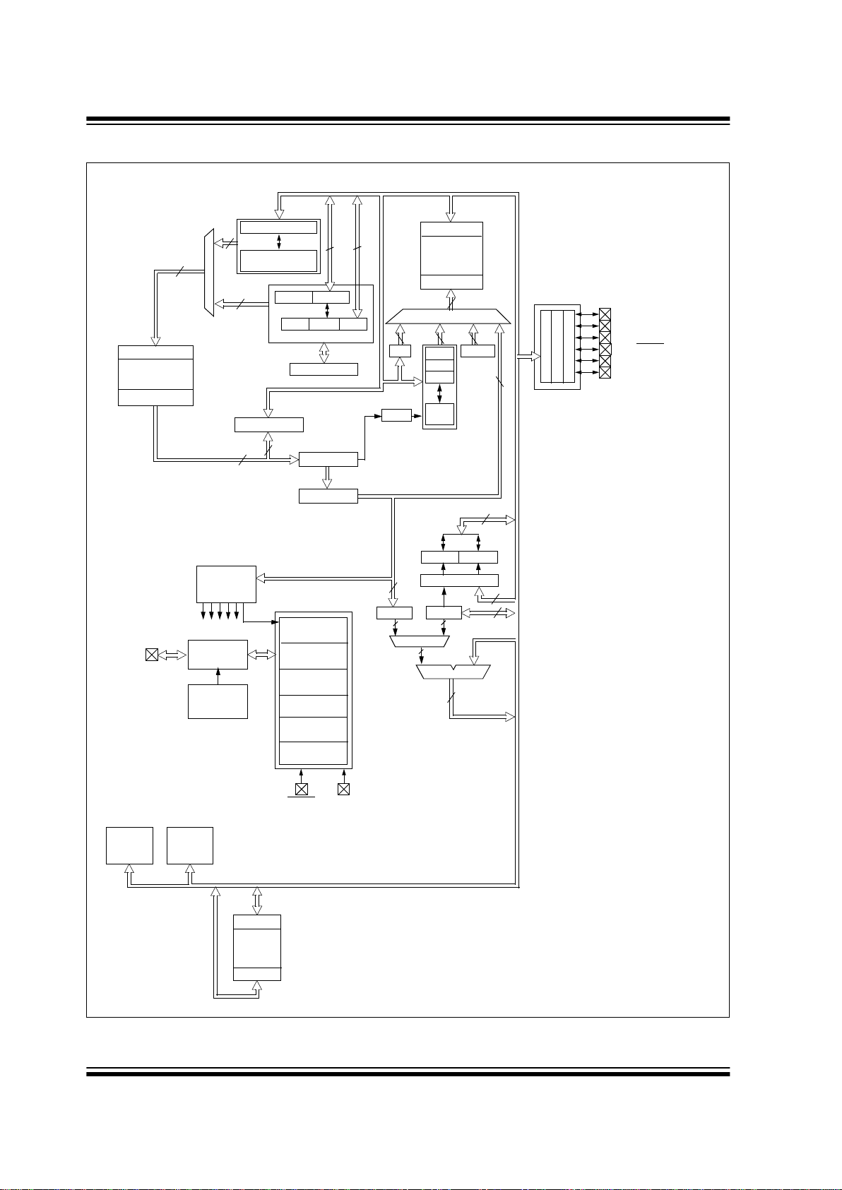
1.0 DEVICE OVERVIEW
This document co nta i ns dev ice sp ec if i c in for m at ion fo r
the PIC18F010/020 microcontrollers. These devices
come in 8-pin pac kages. Table1-1 is an overview of the
features. Figure 1-1 presents the block diag ram for th e
PIC18F010/020 devices and Table 1-2 gives the pin
descriptions.
TABLE 1-1: DEVICE FEATURES
Features PIC18F010 PIC18F020
Operating Frequency DC - 40 MHz DC - 40 MHz
Program Memory (Bytes) 2K 4K
Program Memory (Instructio ns) 1024 2048
Data Memory (SRAM) 256 256
Data Memory (EEPROM) 64 64
Interrupt Sources 5 5
I/O Ports PORTB (6-bit) PORTB (6-bit)
Timers 1 (8/16-bit) 1 (8/16-bit)
RESETS (and Delays) POR, BOR,
RESET Instruction,
Stack Full,
Stack Underflow
(PWRT, OST)
POR, BOR,
RESET Instruction,
Stack Full,
Stack Underflow
(PWRT, OST)
Programmable Low Voltage Detect Yes Yes
Programmable Brown-out Reset Yes Yes
Instruction Set 75 75
Packages 8-pin PDIP
8-pin SOIC
8-pin PDIP
8-pin SOIC
PIC18F010/020
DS41142A-page 4 Preliminary 2001 Microchip Technology Inc.
FIGURE 1-1: PIC18F010/020 BLOCK DIAGRAM
Power-up
Timer
Oscillator
Start-up Timer
Power-on
Reset
Watchdog
Timer
Instruction
Decode &
Control
OSC1/CLKIN
OSC2/CLKOUT
MCLR
VDD, VSS
PORTB
RB0/ICSPDAT
RB4/OSC2/CLKOUT
Brown-out
Reset
Timer0
Timing
Generation
RB1/ICSPCLK
Data Latch
Data RAM
256 bytes
Address Latch
Address<12>
12
Bank0,F
BSR
FSR0
FSR1
FSR2
inc/dec
logic
Decode
4
12
4
PCH PCL
PCLATH
8
31 Level Stack
Program Counter
PRODLPRODH
8 x 8 Multiply
W
8
BITOP
8
8
ALU<8>
8
Te st Mode
Select
Address Latch
Program Memory
(4 Kbytes)
Data Latch
20
21
16
8
8
8
Table Pointer<21>
inc/dec logic
21
8
Data Bus<8>
Table Latch
8
IR
12
3
ROM Latch
RB2/T0CKI/INT0
RB3/MCLR/VPP
PCLATU
PCU
RB5/OSC1/CLKIN
BOR
PLVD
Internal
DATA
EEPROM
64 bytes
EEDATA
EEADDR
Oscillator
2001 Microchip Technology Inc. Preliminary DS41142A-page 5
PIC18F010/020
TABLE 1-2: PIC18F010/020 PRODUCT PINOUT OVERVIEW
Bondpad Name
Devices
Function/Description
8-Pin PDIP 8-Pin SOIC
V
DD 11Power
V
SS 8 8 Ground
RB5/OSC1/CLKIN 2 2 Bi-directional I/O pin (TTL) with optional interrupt-on-change, clock
input, or oscillator input
RB4/OSC2/CLKOUT 3 3 Bi-directional I/O pin (TTL) with optional interrupt-on-change,
oscillator output, or CLKOUT output
RB3/MCLR
/VPP 4 4 Bi-directional I/O pin (TTL), open drain, with optional
interrupt-on-change, or Master Clear External Reset input (ST)
RB2/T0CKI/INT0 5 5 Bi-directional I/O pin (TTL) with optional interrupt-on-change, TMR0
clock input (ST), or interrupt input (ST)
RB1 6 6 Bi-directional I/O pin (TTL) with optional interrupt-on-change
RB0 7 7 Bi-directional I/O pin (TTL) with optional interrupt-on-change

PIC18F010/020
DS41142A-page 6 Preliminary 2001 Microchip Technology Inc.
NOTES:
2001 Microchip Technology Inc. Preliminary DS41142A-page 7
PIC18F010/020
2.0 OSCILLATOR
CONFIGURATIONS
2.1 Oscillator Types
The PIC18F010/020 can be operated in eight different
oscillator modes. Programming these modes is done
via the CONFIG1H register (FOSC2, FOSC1, and
FOSC0).
1. LP Low Power Crystal
2. XT Crystal/Resonator
3. HS High Speed Crystal/Resonator
4. EC External Clock
5. RC External Resistor/Capa citor
6. RCIO External Resistor/Capacitor with
I/O pin enabled
7. INTOSC Precision Internal Oscillator
8. INTOSCIO Precision Internal Oscillator with
I/O pin enabled
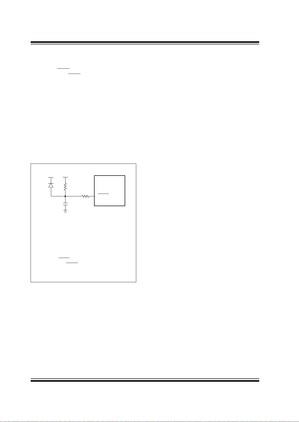
2.2 Crystal Oscillator/Ceramic
Resonators
In XT, LP, or HS oscillator modes, a crystal or ceramic
resonator is connected to the RB5/OSC1 and RB4/
OSC2 pins to establish oscillation. Figure 2-1 shows the
pin connections. An external clock source may also be
connected to the OSC1 pin in these modes, as sh own in
Figure 2-2.
The PIC18F010/020 oscillator design requires the use
of a parallel cut crystal.
FIGURE 2-1: CRYSTAL/CERAMIC
RESONATOR OPERATION
(HS, XT OR LP
OSC CONFIGURATION)
FIGURE 2-2: EXTERNAL CLOCK INPUT
OPERATION (HS, XT OR
LP OSC CONFIGURATION)
Note: Use of a series cut crystal may give a fre-
quency out of the crystal manufacturers
specifications.
Note 1: See Table 2-1 and Table 2-2 for recom-
mended values of C1 and C2.
2: A series resistor (R
S) may be required for AT
strip cut crystals.
3: R
F varies with the crystal chosen.
C1
(1)
C2
(1)
XTAL
OSC2
OSC1
RF
(3)
SLEEP
To
logic
RS
(2)
internal
RB5/OSC1
RB4/OSC2
Open
Clock from
ext. system
PIC18F010/020
PIC18F010/020
DS41142A-page 8 Preliminary 2001 Microchip Technology Inc.
TABLE 2-1: CERAMIC RESONATORS
TABLE 2-2: CAPACITOR SELECTION FOR
CRYSTAL OSCILLATOR
2.3 RC Oscillator
For applications where precise timing is not a requirement, the RC and RCI O oscillator option s are availabl e.
The operation and functionality of the RC oscillator is
dependent on a number of varia bles. The RC oscil lat or
is a function of the supply voltage, the resistor (REXT)
and capacitor (C
EXT) values, and the operating temper-
ature. The oscillator fre quency will va ry from unit to unit
due to normal process parameter variation. Plus, the
difference in le ad fram e c apacitance betw ee n package
types will also affect the oscillation frequency, especially for low C
EXT values. The user also needs to
account for the tolerance of the external R and C components. Figure2-3 shows how the R /C comb inat ion i s
connected.
FIGURE 2-3: RC OSCILLATOR MODE
In the RC mode, the oscilla tor frequen cy divi ded by 4 is
available on the OS C2 pin. This signal ma y be used for
test purposes, or to synchronize other logic. In the
RCIO mode, the OSC2 pin be comes a general purp ose
I/O pin. This pin is RB4 of PORTB.
2.4 The Internal Oscillator
The INTOSC and INTOSCIO device options are available to minimize part count and cost, wh ile ma xim iz in g
the number of I/O pins. There are five d ifferent frequencies of which the user h as the opti on to select. They ar e
32 kHz, 500 kHz, 1 MHz, 4 MHz, and 8 MHz. The 1
MHz, 4 MHz, and 8 MHz internal clock selections are
all derived from one 8 MHz clo ck sou rce, and the other
two are produced ind ependently. T uning is available for
the 1 MHz, 4 MHz, and 8 MHz options; refer to
Section 2.10.
Ranges Tested:
Mode Freq. OSC1 OSC2
XT 455 kHz
2.0 MHz
4.0 MHz
68 - 100 pF
15 - 68 pF
15 - 68 pF
68 - 100 pF
15 - 68 pF
15 - 68 pF
HS 8.0 MHz
16.0 MHz
10 - 68 pF
10 - 22 pF
10 - 68 pF
10 - 22 pF
These values are for design guidance only.
See notes at bottom of page.
Resonators Used:
455 kHz Panasonic EFO-A455K04B ± 0.3%
2.0 MHz Murata Erie C SA2.00MG ± 0.5%
4.0 MHz Murata Erie C SA4.00MG ± 0.5%
8.0 MHz Murata Erie CSA8.00MT ± 0.5%
16.0 MHz Murata Erie CSA16.00MX ± 0.5%
All resonators used did not have built-in capacitors.
Osc Type
Crystal
Freq.
Cap. Range
C1
Cap.
Range C2
LP 32.0 kHz 33 pF 33 pF
200 kHz 15 pF 15 pF
XT 200 kHz 47-68 pF 47-68 pF
1.0 MHz 15 pF 15 pF
4.0 MHz 15 pF 15 pF
HS 4.0 MHz 15 pF 15 pF
8.0 MHz 15- 33 pF 15-33 pF
20.0 MHz 15-33 pF 15-33 pF
25.0 MHz TBD TBD
These val ues are for de sign guidance only.
See notes at bottom of page.
Crystals Used
32.0 kHz Epson C-001R32.768K-A ± 20 PPM
200 kHz STD XTL 200.000KHz ± 20 PPM
1.0 MHz ECS ECS-10-13-1 ± 50 PPM
4.0 MHz ECS ECS-40-20-1 ± 50 PPM
8.0 MHz EPSON CA-301 8.000M-C ± 30 PPM
20.0 MHz EPSON CA-301 20.000M-C ± 30 PPM
Note 1: Recommended values of C1 and C2 are
identical to the ranges tested (Table 2-1).
2: Higher capacitance increases the stability
of the oscillator, but also increases the
start-up time.
3: Since each resonator/crystal has its own
characteristics , the user sh ould co nsult the
resonator/crystal manufacturer for appropriate values of external components.
4: Rs may be required in HS mode, as well as
XT mode, to avoid overdriv ing crys tals with
low drive level specification.
Note: The RC oscillator is not recommended for
applications that require precise timing.
OSC2/CLKO
CEXT
REXT
PIC18F010/020
OSC1
F
OSC/4
Internal
Clock
VDD
VSS
Recommended values: 3 kΩ ≤ REXT ≤ 100 kΩ
C
EXT > 20pF
2001 Microchip Technology Inc. Preliminary DS41142A-page 9
PIC18F010/020
2.5 External Clock Input
The EC oscillator mode requires an external clock
source to be conne cted to the OSC1 pi n. The feedback
device between OSC1 and OSC2 is turned off in this
mode to save current. There is no oscillator start-up
time required after a Power-on Reset or after a recovery from SLEEP mode.
In the EC oscillator mode, the oscillator frequency
divided by 4 is available on the OSC2 pin. This signal
may be used for t est pu rp os es or to sy nc hr o niz e o t he r
logic. Figure 2-4 shows the pin connections fo r the EC
oscillator mode.
FIGURE 2-4: EXTERNAL CLOCK INPUT
OPERATION (EC OSC
CONFIGURATION)
FIGURE 2-5: PIC18F010/020 OSCILLATOR CONFIGURATION
OSC1
OSC2
F
OSC/4
Clock from
ext. system
PIC18F010/020
MUX
Configuration bits
OSCOUT
OSCIN
Crystal
Osc
SYSCLK
Ext Osc
and
Divider
82
1
IRCF Speed Selects
MUX
OSCTUNEOSCCAL
+
Analog
Summation
External Clock In
500kHz
Internal
8MHz
Internal
OSC
OSC
32kHz
Internal
OSC

PIC18F010/020
DS41142A-page 10 Preliminary 2001 Microchip Technology Inc.
2.6 Two-Speed Clock Start-up Mode
In order to minimize the latency between oscillator
start-up and code execution, a mode which allows the
system clock to initially use the internal clock, may be
selected with IESO (Internal-External Switchover) bit.
In this mode and upon RESET, the system will begin
execution with the internal oscillator at the frequency
selected by the IRCFx bits of the OSCCON register.
After the OST h as timed o ut, a glitchle ss switcho ver will
be made to the oscillator mode selected by F
OSCx in
the CONFIG1H register. The software may read the
OSTO bit to determine when the switchover takes
place, so that any software timing delays may be
adjusted.
Wake-up from SLEEP causes a unique start-up procedure. The power supply is assumed to be stable, since
neither the POR nor the BOR Resets have been
invoked. This assumption allows the Power-on Timer
(PWRT) time-out to be bypassed, and only the OST
time-out to be used. This results in almost immediate
code execution with the minimum of delay. The internal
oscillator frequency can be selected to be close to final
crystal frequency to reduce timing differences , or a lower
frequency can be chosen to reduce power consumption.
REGISTER 2-1: OSCCON REGISTER (ADDRESS FD3h)
Note: Only on Power-on Reset, the register con-
tents are zeroed by the POR circuitry and
the frequency selectio n is forced to 32 kHz.
The register is not effected by any other
forms of RESET.
U-0 R/W-0 R/W-0 R/W-0 R-0 R/W-0 U-0 R/W-0
— IRCF2 IRCF1 IRCF0 OSTO IESO — SCS
bit 7 bit 0
bit 7 Unimplemented: Read as ‘0’
bit 6-4 IRCF<2:0>: Internal Oscillator Frequency Select bits
000 = 32 kHz
001 = Reserved
010 = Reserved
011 = 500 kHz
100 = 1 MHz
101 = Reserved
110 = 4 MHz
111 = 8 MHz
bit 3 OSTO: Oscillator Start-up Time-out Status bit
1 = Oscillator Start-up Timer has timed out
0 = Oscillator Start-up Timer running
bit 2 IESO: Internal-External Switchover bit
1 = Start with internal oscillator, then switch over to selected oscillator mode after OST
0 = No switch from internal oscillator from RESET
bit 1 Unimplemented: Read as ‘0’
bit 0 SCS: System Clock Switch bit
1 = Clock source comes from internal oscillator input
0 = Clock source comes from external clock source on OSC1
Legend:
R = Readable bit W = Writable bit U = Unimplemented bit, read as ‘0’
- n = Value at POR ’1’ = Bit is set ’0’ = Bit is cleared x = Bit is unknown
Note: This register must be unlocked to modify, see Section 12.4.
2001 Microchip Technology Inc. Preliminary DS41142A-page 11
PIC18F010/020
2.6.1 OSCILLATOR TRANSITIONS
The PIC18F010/020 devices contain circuitry to prevent "glitches" when switching between oscillator
sources. Essentially, the circuitry waits for eight rising
edges of the clock source that the processor is switching to. This en sures tha t the new clock s ource is stabl e
and that its pulse wid th will no t be less than the sho rtest
pulse width of the two clock sources.
A timing diagram, indicating th e transition f rom the in ternal oscillator to the external crystal is shown in Figure 2-6.
The internal oscillator is assumed to be running all the
time. After the OST bi t is set, the pr oce ssor is froz en at
the next occurring Q1 cycle. Af ter eight synchroniza tion
cycles are counted from the external oscillator, operation resumes. No additional delays are required after
the synchronization cycles.
FIGURE 2-6: TIMING DIAGRAM FOR TRANSITION FROM EXTERNAL OSCILLATOR TO
INTERNAL OSCILLATOR
FIGURE 2-7: TIMING FOR TRANSITION BETWEEN INTERNAL OSCILLATOR AND OSC1 (EC)
Q3Q2Q1Q4Q3Q2
OSC1
Internal
OSTO
(OSCCON<0>)
Program
PC + 2PC
Note 1: Delay on internal system clock is eight oscillator cycles for synchronization.
INTOSC
Q4 Q1
PC + 4
Q1
Clock
Counter
System
Q2 Q3 Q4 Q1
TOSC
21 34 5678
Q3 Q4
Q1
Q1 Q2 Q3 Q4 Q1 Q2 Q3
OSC1
Internal System
SCS
(OSCCON<0>)
Program Counter
PC PC + 2
Note 1: Internal oscillator mode assumed.
PC + 4
INTOSC
Clock
OSC2
Q4
TOSC
1
23
45678

PIC18F010/020
DS41142A-page 12 Preliminary 2001 Microchip Technology Inc.
2.7 Effects of SLEEP Mode on the
On-chip Oscillator
When the device exe cutes a SLEEP i nstructio n, the onchip clocks and oscillator are turn ed off and the device
is held at the beginning of an instruction cycle (Q1
state). With the oscill ato r of f, the OSC 1 and OS C2 si gnals will stop oscill ating. Since all the transis tor s w itch-
ing currents have been removed, SLEEP mode
achieves the lowest current consumption of the device
(only leakage currents). Enabling any on-chip feature
that will operate during SL EEP will increas e the current
consumed during SLEEP. The user can wake from
SLEEP through external RESET, Watchdog Timer
Reset or through an interrupt.
TABLE 2-3: OSC1 AND OSC2 PIN STATES IN SLEEP MODE
OSC Mode OSC1 Pin OSC2 Pin
Internal Oscillator Floating, external resistor should pull
high
At logic low
RCIO Floating, external resistor should pull
high
Configured as PORTB, RB4
EC Floating At logic low
LP, XT, and HS Feedback inverter disabled, at quiescent
voltage level
Feedback inverter disabled, at quiescent
voltage level
Note: See Table 3-1 in the RESET Section, for time-outs due to SLEEP and MCLR
Reset.

2001 Microchip Technology Inc. Preliminary DS41142A-page 13
PIC18F010/020
2.8 Power-up Delays
Power-up delays are controlled by two timers, so that
no external RESET circuitry is required for most applications. The delays ensure that the device is kept in
RESET until the device power sup ply and clock are st able. For additional information on RESET operation,
see the “RESET” section.
The first timer is the Power-up Timer (PWRT), which
optionally provides a fix ed delay of 72 ms (nominal) on
power-up only (POR and BOR). The second timer is
the Oscillator Start-up Timer OST, intended to keep the
chip in RESET until the crystal oscillator is stable.
2.9 Frequency Calibrations
The 8 MHz frequency is cali brated at the fact ory. Since
the 4 MHz and 1 MHz cloc k outputs are derived digita lly
from the 8 MHz, the accuracy specifications of the 4
MHz and 1 MHz clocks are the same as the 8 MHz.
The 500 kHz and 32 kHz frequencies are not calibrated. The 500 kHz and 32 kHz are nominal frequencies. Their accuracy specifications are shown in the
Specifications section.
2.10 Frequency Tuning in User Mode
In addition to the factory calibration, 8 MHz frequency
can be tuned in the user’s application. This frequency
tuning capabili ty allows user to deviate from the fac tory
calibrated frequency. The user can tune the frequency
by writing to the OSCTUNE register. See Register 2-2
for details of the OSCTUNE register. The tuning range
of the 8 MHz oscillator is ±1 MHz, or ±12.5% nominal.
See the Specifications section for further specification
details.
Since the 4 MHz and 1 MHz are derived from the 8
MHz, the tuning range of the 4 MHz is ±500 kHz nominal, and the tuning range of the 1 MHz is ±125 kHz
nominal. The tuning sensitivity (%F
INTOSC/bit) is con-
stant throughout the frequency selections and tuning
range.
REGISTER 2-2: OSCTUNE REGISTER (ADDRESS 0F9Bh)
Note: Frequency tuning is not available in the
500 kHz and 32 kHz frequencies.
U-0 U-0 R/W-0 R/W-0 R/W-0 R/W-0 R/W-0 R/W-0
— — TUN5 TUN4 TUN3 TUN2 TUN1 TUN0
bit 7 bit 0
bit 7-6 Unimplemented: Read as ‘0’
bit 5-0
TUN<5:0>: 6-bit Frequency Tuning
011111 = Maximum frequency
011110
•
•
•
000001
000000 = Center frequency. Oscillator module is running at the calibrated frequency.
111111
•
•
•
100000 = Minimum frequency
Legend:
R = Readable bit W = Writable bit U = Unimplemented bit, read as ‘0’
- n = Value at POR ’1’ = Bit is set ’0’ = Bit is cleared x = Bit is unknown

PIC18F010/020
DS41142A-page 14 Preliminary 2001 Microchip Technology Inc.
2.11 Base Frequency Change
There are two methods to change frequency during
normal program operation. One option is to switch frequencies using the internal oscillator only; IRCF<2:0>
in the OSCCON register selects the internal oscillator
frequency. Refer to Register 2-1.
Switching for an external clock to an internal oscillator
and vice versa is also possible. Use the SCS bit in the
OSCCON register to select an external or internal cl ock
source.
2.12 Oscillator Delay Upon Start-up
and Base Frequency Change
When the INTOSC Oscillator Module starts up, an
8-cycle delay of the base frequency is invoked. During
this delay, the FINTOSC output signal is held at ‘0’.
The INTOSC Oscillator Module also allows user to
change frequency during run time. For example, the
frequency can be ch anged from 8 M Hz to 32 kH z, while
the device is operating. When the application requires
a base frequency change, a delay of 8 cycles of the
new base frequency is invoked.
Writing to the OSCTUNE register will not cause any
delay. In applications where the OSCTUNE register is
used to shift the F
INTOSC frequency, the application
should not expect the F
INTOSC frequency to stabilize
immediately. In this case, the frequency m ay shif t gradually toward the n ew v al ue. The time for this freque nc y
shift is less than 8 cycles of the base frequency.
Table 2-4 below, shows examples of when the oscillator delay is invoked.
TABLE 2-4: OSCILLATOR DELAY EXAMPLES
Note: The OSCEN bit in the CONFIG 1H configu-
ration byte must be set to allow clock
switching.
Old Frequency New Frequency
New Base
Frequency
Oscillator Delay Comments
8 MHz 4 MHz or 1 MHz No None The 8 MHz, 4 MHz, and 1 MHz are all
running from the same 8 MHz base
frequency.
500 kHz 32 kHz 32 kHz 250µS nominal Base frequency changes from 500 kHz
to 32 kHz.
4 MHz 32 kHz 32 kHz 250µS nominal Base fr equ enc y ch anges from 8 MHz to
32 kHz.
500 kHz 8 MHz 8 MHz 1µS nominal Base frequency changes from 500 kHz
to 8 MHz.
Off or SLEEP
mode
1 MHz 8 MHz 1µS nominal Upon power-up and wake-up from
SLEEP, there is always oscillator delay.
Off or SLEEP
mode
500 kHz 500 kHz 16µS nominal Upon power-up and wake-up from
SLEEP, there is always oscillator delay.
2001 Microchip Technology Inc. Preliminary DS41142A-page 15
PIC18F010/020
3.0 RESET
The PIC18F010/020 differentiates between various
kinds of RESET:
a) Power-on Reset (POR)
b) MCLR
Reset during normal operation
c) MCLR Reset during SLEEP
d) Watchdog Timer (WDT) Reset (during normal
operation)
e) Programmable Brown-out Reset (BOR)
f) RESET Instruction
g) Stack Full Reset
h) Stack Underflow Reset
Most registers are una ffected b y a RESET. Their status
is unknown on POR and unchanged by all other
RESETS. The other registers are forced to a “RESET
state” on Power-on Reset, MCLR
, WDT Reset, Brown-
out Reset, MCLR
Reset during SLEEP and by the
RESET instruction.
Most registers are not affected by a WDT wake-up,
since this is viewed as the resumption of normal operation. Status bits from the RCON register, RI
, TO, PD,
POR
and BOR, are set or cleared differently in different
RESET situations, as i ndicated in Table 3-2. These bit s
are used in software to determine the nature of the
RESET. See Table 3-3 for a full description of the
RESET states of all registers.
A simplified block diagram of the on-chip RESET circuit
is shown in Figure 3-1.
The Enhanced MCU devices have a MCLR
noise filter
in the MCLR
Reset path. The filter will detect and
ignore small pulses.
FIGURE 3-1: SIMPLIFIED BLOCK DIAGRAM OF ON-CHIP RESET CIRCUIT
S
R
Q
External Reset
MCLR
WDT
Module
V
DD Rise
Detect
OST/PWRT
On-chip
Internal Osc
(1)
WDT
Time-out
Power-on Reset
OST
10-bit Ripple Counter
PWRT
Chip_Reset
10-bit Ripple Counter
Reset
Enable OST
(2)
Enable PWRT
SLEEP
Note 1: This is a separate oscillator from the internal oscillator of the CLKIN pin.
2: See Table3-1 for time-out situations.
Brown-out
Reset
BOREN
RESET
Instruction
Stack
Pointer
Stack Full/Underflow Reset
VDD
OSC1
PIC18F010/020
DS41142A-page 16 Preliminary 2001 Microchip Technology Inc.
3.1 Power-on Reset (POR)
A Power-on Reset pulse is generated on-chip when
V
DD rise is detected. To take advantage of the POR c ir-
cuitry, tie the MCLR
pin directly (or through a resistor)
to V
DD, or disable MCLR. This will eliminate external
oscillator components usually needed to create a
Power-on Reset delay. A maximum rise time for V
DD is
specified (parameter D004). For a slow rise time, see
Figure 3-2.
When the device starts normal operation (exits the
RESET condition), device operating parameters (voltage, frequency, temperature,...) must be met to en su re
operation. If these cond itions are not met, the de vice
must be held in RESET until the operating conditions
are met. Brown-out Reset may be used to meet the
voltage start- up condition.
FIGURE 3-2: EXTERNAL POWER-ON
RESET CIRCUIT (FOR
SLOW V
DD POWER-UP)
3.2 Power-up Timer (PWRT)
The Power-up Timer provides a fixed nominal time-out
(parameter #33) only on power-up from the POR or
BOR, if enabl ed. The Pow er-up Timer o perates on an
internal oscillator . The chi p is kept in RESET as long a s
the PWRT is active. The PWRT’s time delay allows
V
DD to rise to an accep tabl e lev el. A con figurat ion bit i s
provided to enable/disable the PWRT.
The power-up time delay wil l vary from chip-to-ch ip due
to V
DD, temperature and process variation. See DC
parameter #33 for details.
3.3 Oscillator Start-up Timer (OST)
The Oscillator Start-up Timer (OST) provides 1024
oscillator cycle (from OSC1 input) delay after the
PWRT delay is over (para meter #32). This ensures th at
the crystal oscillator or resonator has started and
stabilized.
The OST time-out is invoked only for XT, LP and HS
modes and only on Power-on Reset or wake-up from
SLEEP.
3.4 Brown-out Reset (BOR)
A configuration bit, BOREN, can disable (if clear/
programmed), or enable (if set) the Brown-out Reset
circuitry. If VDD falls below parameter D005 for greater
than parameter #35, the brown-out situation will reset
the chip. A RESET may not occur if V
DD falls below
parameter D005 for less than p arameter #35. The chip
will remain in Brown-out Reset until V
DD rises above
BV
DD. The Power- up Timer will then be invok ed and
will keep the chip in RESET an additional time delay
(parameter #33). If V
DD drops below BVDD while the
Power-up Timer is running, the chip will go back into a
Brown-out Reset and the Power-up T im er will be initialized. Once V
DD rises above BVDD, the Power-up Timer
will execute the additional time delay.
Note 1: External Power-on Reset circuit is required only
if the V
DD power-up slope is too slow. T he diode
D helps discharge the capacitor quickly when
V
DD powers down.
2: R < 40k
Ω is recommended to make sure that
the voltage drop across R does not violate the
device’s electrical specification.
3: R1 = 100
Ω to 1kΩ will limit any current flowing
into MCLR
from external capacitor C, in the
event of MCLR/
VPP pin breakdown due to
Electrostatic Discharge (ESD), or Electrical
Overstress (EOS).
C
R1
R
D
V
DD
MCLR
PIC18F010/020
2001 Microchip Technology Inc. Preliminary DS41142A-page 17
PIC18F010/020
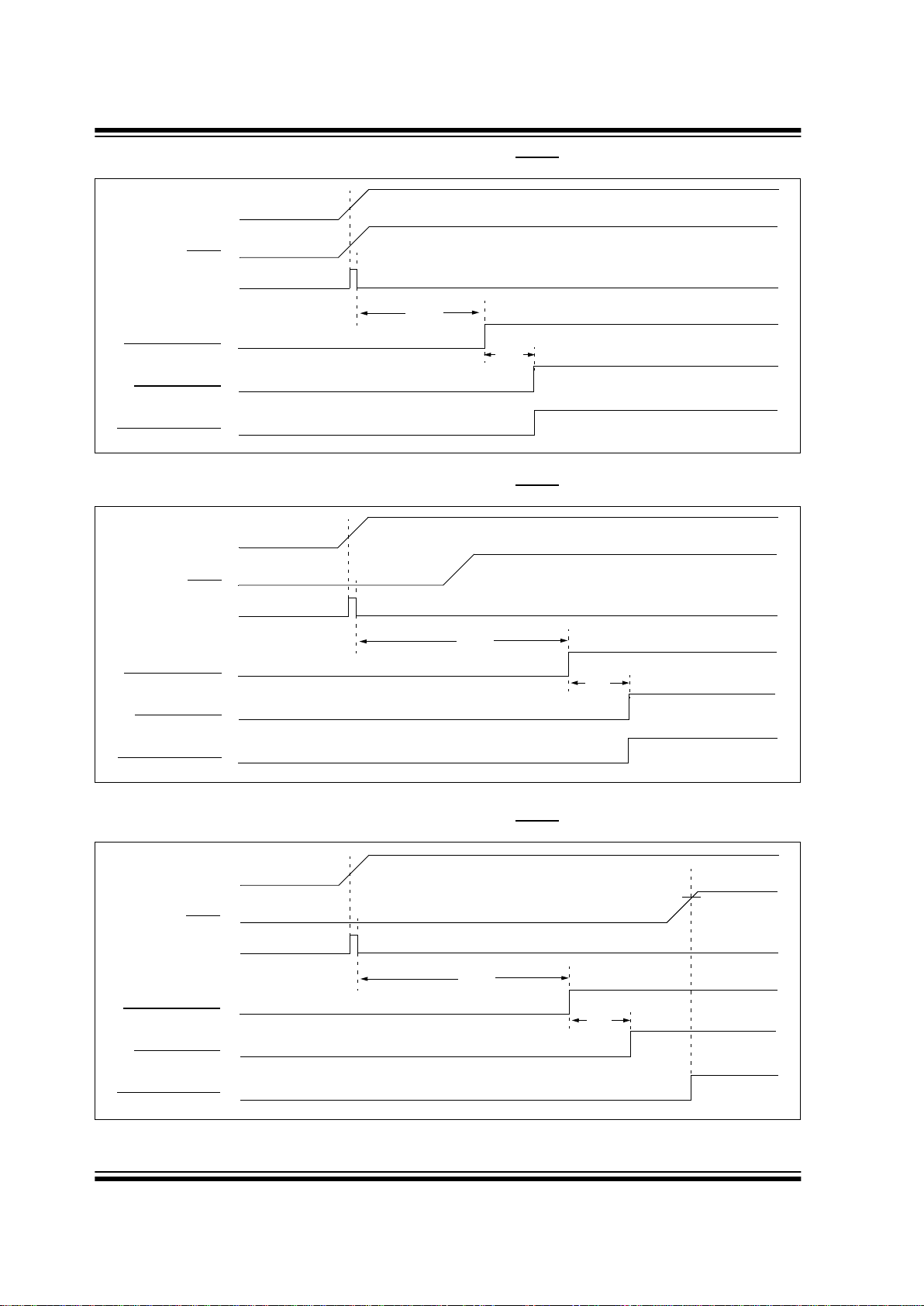
3.5 Time-out Sequence
On power-up, the time-ou t sequenc e is as foll ows: first,
PWRT time-out is invoked af ter the POR time delay has
expired; then, OST is activated. The total time-out will
vary based on oscillator con figura tion and the st atus of
the PWRT. For example, in Internal Oscillator mode
with the PWRT disabled , there will be no time-o ut at all.
Figure 3-3, Figure 3-4, Figure 3-5 and Figure 3-6
depict time-out sequences on power-up.
Since the time-outs occur from the PO R pulse, if MCLR
is kept low long enough, the time-outs will expire.
Bringing MCLR
high will begin execution immediately
(Figure 3-5). This is useful for testing purposes or to
synchronize more than one PIC18F010/020 device
operating in parallel.
Table 3-2 shows the RESET conditions for some
Special Function Registers, while Table 3-3 shows the
RESET conditions for all the registers.
TABLE 3-1: TIME-OUT IN VARIOUS SITUATIONS
REGISTER 3-1: RCON REGISTER BITS AND POSITIONS
TABLE 3-2: STATUS BITS, THEIR SIGNIFICANCE AND THE INITIALIZATION CONDITION FOR
RCON REGISTER
Oscillator
Configuration
Power-up
(1)
Brown-out
(1)
Wake-up from
SLEEP or
Oscillator Switch
PWRTE
= 0 PWRTE = 1
HS, XT, LP 72 ms + 1024Tosc 1024Tosc 72 ms + 1024Tosc 1024Tosc
EC 72 ms — 72 ms —
External Oscillator 72 ms — 72 ms —
Internal Oscillator
(2)
72 ms — 72 ms —
Note 1: 72 ms is the nominal power-up timer delay.
2: 8-cycle delay.
R/W-0 U-0 U-0 R/W-1 R-1 R-1 R/W-1 R/W-1
IPEN — — RI TO PD POR BOR
bit 7 bit 0
Condition
Program
Counter
RCON
Register
RI
TO PD POR BOR STKFUL STKUNF
Power-on Reset 0000h 00-1 1100 1 1 1 0 0 u u
MCLR
Reset during normal
operation
0000h 00-u uuuu u u u u u u u
Software Reset during normal
operation
0000h 0u-0 uuuu 0 u u u u u u
Stack Full Reset during normal
operation
0000h 0u-u uu11 u u u u u 1 u
Stack Underflow Reset during
normal operation
0000h 0u-u uu11 u u u u u u 1
MCLR
Reset during SLEEP 0000h 00-u 10uu u 1 0 u u u u
WDT Reset 0000h 0u-u 01uu 1 0 1 u u u u
WDT Wake-up PC + 2 uu-u 00uu u 0 0 u u u u
Brown-out Reset 0000h 0u-1 11u0 1 1 1 1 0 u u
Interrupt Wake-up from SLEEP
PC + 2
(1)
uu-u 00uu u 1 0 u u u u
Legend: u = unchanged, x = unknown, - = unimplemented bit, read as '0'.
Note 1: When the wake-up is due to an interrupt and the GIEH or GIEL bits are set, the PC is loaded with the
interrupt vector (0x000008h or 0x000018h).

PIC18F010/020
DS41142A-page 18 Preliminary 2001 Microchip Technology Inc.
TABLE 3-3: INITIALIZATION CONDITIONS FOR ALL REGISTERS
Register
Power-on Reset,
Brown-out Reset
MCLR
Reset
WDT Reset
Reset Instruction
Stack Reset
Wake-up via WDT
or Interrupt
TOSH 0000 0000 0000 0000
uuuu uuuu
(3)
TOSL 0000 0000 0000 0000
uuuu uuuu
(3)
STKPTR 00-0 0000 00-0 0000
uu-u uuuu
(3)
PCLATU ---0 0000 ---0 0000 ---u uuuu
PCLATH 0000 0000 0000 0000 uuuu uuuu
PCL 0000 0000 0000 0000
PC + 2
(2)
TBLPTRU ---0 00-- ---0 00-- ---u uu--
TBLPTRH ---- 0000 ---- 0000 ---- uuuu
TBLPTRL 0000 0000 0000 0000 uuuu uuuu
TABLAT 0000 0000 0000 0000 uuuu uuuu
PRODH xxxx xxxx uuuu uuuu uuuu uuuu
PRODL xxxx xxxx uuuu uuuu uuuu uuuu
INTCON 0000 000x 0000 000u
uuuu uuuu
(1)
INTCON2 11-- -1-1 11-- -1-1
uu-- -u-u
(1)
INDF0 N/A N/A N/A
POSTINC0 N/A N/A N/A
POSTDEC0 N/A N/A N/A
PREINC0 N/A N/A N/A
PLUSW0 N/A N/A N/A
FSR0H ---- 0000 ---- 0000 ---- uuuu
FSR0L xxxx xxxx uuuu uuuu uuuu uuuu
WREG xxxx xxxx uuuu uuuu uuuu uuuu
INDF1 N/A N/A N/A
POSTINC1 N/A N/A N/A
POSTDEC1 N/A N/A N/A
PREINC1 N/A N/A N/A
PLUSW1 N/A N/A N/A
FSR1H ---- 0000 ---- 0000 ---- uuuu
FSR1L xxxx xxxx uuuu uuuu uuuu uuuu
BSR ---- 0000 ---- 0000 ---- uuuu
INDF2 N/A N/A N/A
POSTINC2 N/A N/A N/A
POSTDEC2 N/A N/A N/A
PREINC2 N/A N/A N/A
PLUSW2 N/A N/A N/A
Legend: u = unchanged, x = unknown, - = unimplemented bit, read as ’0’, q = value depends on condition
Note 1: One or more bits in the INTCONx or PIRx registers will be affected (to cause wake-up).
2: When the wake-up is due to an inte rrupt a nd the GIEL or GIEH bit is set, the PC is lo aded with the i nterrupt
vector (0008h or 0018h).
3: When the wake-up is due to an interrupt and the GIEL or GIEH bit is set, the TOSU, TOSH and TOSL are
updated with the current value of the PC. The STKPTR is modified to point to the next location in the hardware stack.
4: See Table3-2 for RESET value for specific condition.
5: The long write enable is only reset on a POR or MCLR
Reset.

2001 Microchip Technology Inc. Preliminary DS41142A-page 19
PIC18F010/020
FSR2H ---- 0000 ---- 0000 ---- uuuu
FSR2L xxxx xxxx uuuu uuuu uuuu uuuu
ST ATUS ---x xxxx ---u uuuu ---u uuuu
TMR0H 0000 0000 0000 0000 uuuu uuuu
TMR0L xxxx xxxx uuuu uuuu uuuu uuuu
T0CON 1111 1111 1111 1111 uuuu uuuu
OSCCON -000 00-0 -uuu uu-u -uuu uu-u
LVDCON --00 0101 --00 0101 --uu uuuu
WDTCON ---- ---0 ---- ---0 ---- ---u
RCON
(4,5)
0--1 11qq 0--q qquu u--u qquu
IPR2 ---- 1111 ---- 1111 ---- uuuu
PIR2 ---- 0000 ---- 0000
---- uuuu
(1)
PIE2 ---- 0000 ---- 0000 ---- uuuu
TRISB --11 1111 --11 1111 --uu uuuu
LATB --xx xxxx --uu uuuu --uu uuuu
PORTB --xx xxxx --uu uuuu --uu uuuu
PSPCON ---- --00 ---- --00 ---- --uu
EEADR xxxx xxxx uuuu uuuu uuuu uuuu
EEDATA xxxx xxxx uuuu uuuu uuuu uuuu
EECON2 ---- ---- ---- ---- ---- ---EECON1 x--0 x000 u--0 u000 u--u uuuu
OSCTUNE --00 0000 --qq qqqq --uu uuuu
WPUB --11 1111 --11 1111 --uu uuuu
IOCB --00 0000 --00 0000 --uu uuuu
TABLE 3-3: INITIALIZATION CONDITIONS FOR ALL REGISTERS (CONTINUED)
Register
Power-on Reset,
Brown-out Reset
MCLR
Reset
WDT Reset
Reset Instruction
Stack Reset
Wake-up via WDT
or Interrupt
Legend: u = unchanged, x = unknown, - = unimplemented bit, read as ’0’, q = value depends on condition
Note 1: One or more bits in the INTCONx or PIRx registers will be affected (to cause wake-up).
2: When the wake-up is due to an inte rrupt a nd the GIEL or GIEH bit is set, the PC is lo aded with the i nterrupt
vector (0008h or 0018h).
3: When the wake-up is due to an interrupt and the GIEL or GIEH bit is set, the TOSU, TOSH and TOSL are
updated with the current value of the PC. The STKPTR is modified to point to the next location in the hard-
ware stack.
4: See Table3-2 for RESET value for specific condition.
5: The long write enable is only reset on a POR or MCLR
Reset.
PIC18F010/020
DS41142A-page 20 Preliminary 2001 Microchip Technology Inc.
FIGURE 3-3: TIME-OUT SEQUENCE ON POWER-UP (MCLR TIED TO VDD)
FIGURE 3-4: TIME-OUT SEQUENCE ON POWER-UP (MCLR
NOT TIED TO VDD): CASE 1
FIGURE 3-5: TIME-OUT SEQUENCE ON POWER-UP (MCLR
NOT TIED TO VDD): CASE 2
TPWRT
TOST
VDD
MCLR
INTERNAL POR
PWRT TIME-OUT
OST TIME-OUT
INTERNAL RESET
VDD
INTERNAL RESET
TPWRT
TOST
VDD
MCLR
INTERNAL POR
PWRT TIME-OUT
OST TIME-OUT
INTERNAL RESET
VDD
MCLR
INTERNAL POR
PWRT TIME-OUT
OST TIME-OUT
INTERNAL RESET
TPWRT
TOST
2001 Microchip Technology Inc. Preliminary DS41142A-page 21
PIC18F010/020
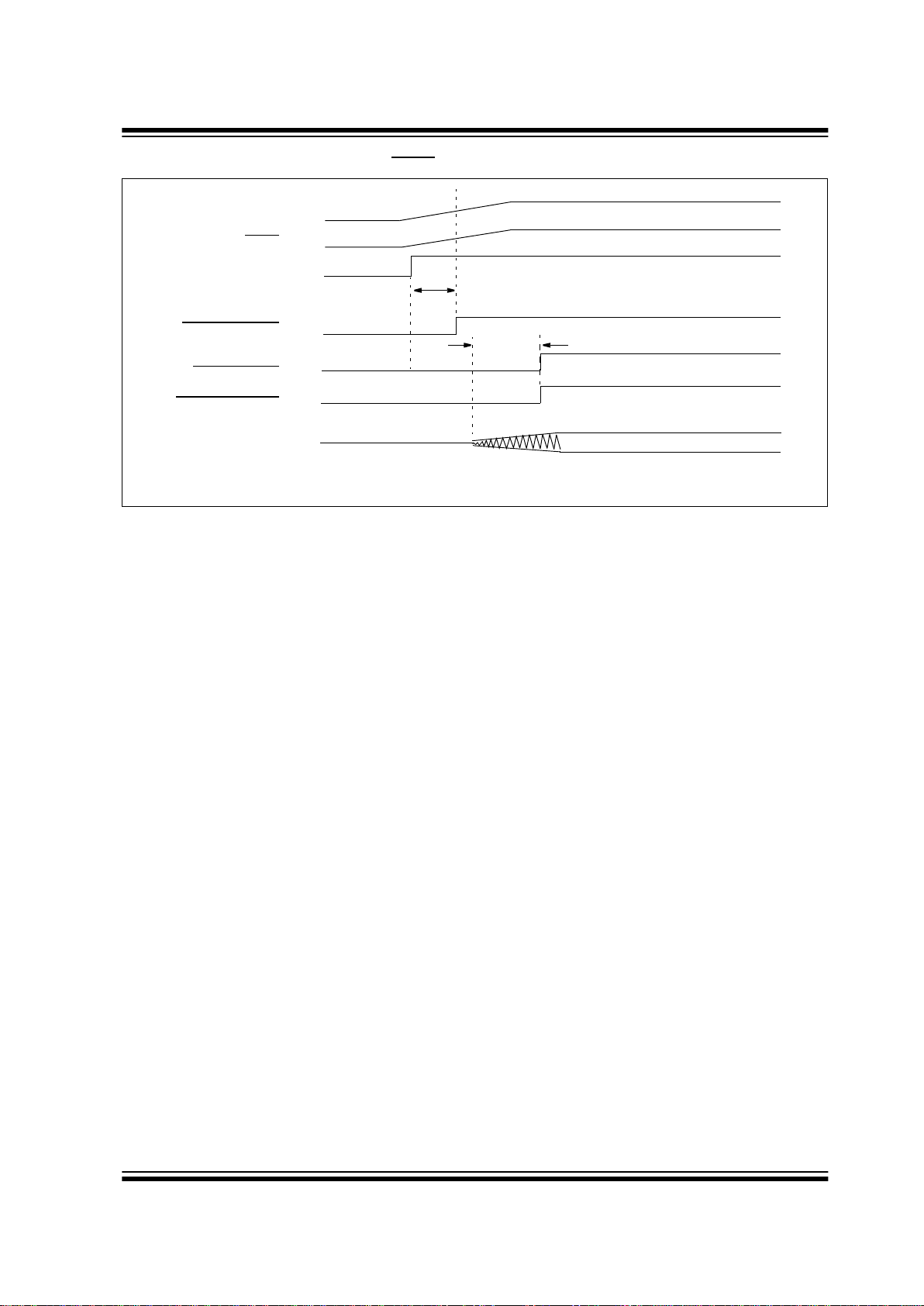
FIGURE 3-6: SLOW RISE TIME (MCLR TIED TO VDD)
VDD
MCLR
INTERNAL POR
PWRT TIME-OUT
OST TIME-OUT
INTERNAL RES ET
0V
1V
5V
T
PWRT
TOST
OSCILLATOR
Note: For slow starting crystals, OST can start beyond PWRT.

PIC18F010/020
DS41142A-page 22 Preliminary 2001 Microchip Technology Inc.
NOTES:

2001 Microchip Technology Inc. Preliminary DS41142A-page 23
PIC18F010/020
4.0 MEMORY ORGANIZATION
There are three memory blocks in PIC18F010/020
Enhanced MCU devices. These memory blocks are:
• Program Memory
• Data Memory
• EEPROM Data Memory
The EEPROM Data Memory is described in detail in
Section 5.0.
4.1 Program Memory Organization
The PIC18F010/020 devices have a 21-bit program
counter. Bits 12 through 16 are implemented as ‘0’
internally; therefore, accessing locations 0x01000
through 0x1FFFF actually mirror what is present in program memory from 0x0000 through 0x0FFF. The
PIC18F010 device reads all zeros (NOP) from 0x0800
through 0x 0FFF.
PIC18F020 has 4 Kbytes of FLASH program memory,
while PIC18F010 has 2 Kbytes of FLASH program
memory . This means the PIC18F020 can st ore up to 2K
of single word instructions, and the PICF18010 can
store up to 1K of single word instructions.
The RESET vector address is at 0000h and the interrupt vector addresses are at 0008h and 0018h. 0008h
is the high priority interru pt and 0018h is the low pri ority
interrupt vector.
Figure 4-1 shows the Program Memory Map for
PIC18F010 and Figure4-2 shows the Program Memory Map for PIC18F020 devices.
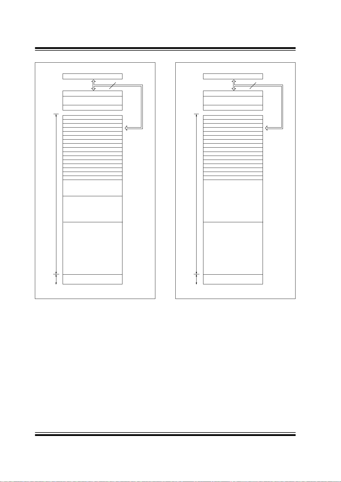
PIC18F010/020
DS41142A-page 24 Preliminary 2001 Microchip Technology Inc.
FIGURE 4-1: PIC18F010 MEMORY FIGURE 4-2: PIC18F020 MEMORY
PC<20:0>
Stack Level 1
•
Stack Level 31
RESET Vector LSb
High Priority Interrupt Vector LSb
•
•
User Memory
Space
21
000000h
000008h
000018h
200000h
200003h
1FFFFFh
Low Priority Interrupt Vector LSb
RESET Vector MSb
000001h
High Priority Interrupt Vector MSb
Low Priority Interrupt Vector MSb
000019h
000009h
User ID Locations
User FLASH
001000h
000FFFh
Mirror
0007FFh
000800h
Read ‘0’s
PC<20:0>
Stack Level 1
•
Stack Level 31
RESET Vector LSb
High Priority Interrupt Vector LSb
•
•
User Memory
Space
21
000000h
000008h
000018h
200000h
200003h
1FFFFFh
Low Priority Interrupt Vector LSb
RESET Vector MSb
000001h
High Priority Interrupt Vector MSb
Low Priority Interrupt Vector MSb
000019h
000009h
User ID Locations
User FLASH
001000h
000FFFh
Mirror
Program Memory

2001 Microchip Technology Inc. Preliminary DS41142A-page 25
PIC18F010/020
4.2 Return Address Stack
The return address s tack allows any co mb in ation of up
to 31 program calls and interrupts to occur. The PC
(Program Counter) is pushed onto the stack when a
PUSH, CALL, or RCALL instruction is executed, or an
interrupt is acknowledged. The PC value is pulled off
the stack on a POP, RETURN, RETLW, or a RETFIE
instruction. PCLATU and PCLATH are not affected by
any of the return instructions.
The stack operates as a 31-word by 21-bit RAM with a
5-bit stack pointer. Although there are 21 bits in the
TOS latch, bits 12 through 16 are not physically implemented in the stack and are read as zeros. The stack
pointer initializes to 0x00 after all RESETS, and there
is no RAM associated with stack pointer 0x00. This is
only a RESET value. During a CALL type instruction
causing a push onto the stack, the stack pointer is first
incremented and the RAM location pointed to by the
stack pointer i s written wi th the conte nts of th e PC. During a RETURN type instruction causing a pop from the
stack, the contents of the RAM location pointed to by
the STKPTR is transferred to the PC and then, the
stack pointer is decremented.
The stack space is not part of either program or data
space. The stac k p oi nte r i s r ead ab l e a n d wr i tabl e, a nd
the address on the top of the stac k is readab le and writable through SFR registers. Data can also be pushed
to, or popped from the stack, using the top-of-stack
SFRs. Status bits indicate if the stack pointer is at, or
beyond, the 31 levels provided.
4.2.1 TOP-OF-STACK ACCESS
The top of the stack is readable and writable. Three
register locations, TOSH and TOSL hold the contents
of the stack location pointed to by the STKPTR register.
This allows users to impl ement a softw are stack, if ne cessary . After a CALL, RCALL or interrupt, the sof tware
can read the pushed value by reading the TOSH and
TOSL registers. T hes e values can be place d o n a us er
defined software stack. At return time, the sof tware can
replace the TOSH and TOSL and do a return.
The user must disable the global interrupt enable bits
during this time to prevent inadvertent stack operations.
4.2.2 RETURN STACK POINTER
(STKPTR)
The STKPTR register contains the stack pointer va lu e,
the STKFUL (stack full) status bit, and the STKUNF
(stack underflow) status bits. Register 4-1 shows the
STKPTR register. The value of the stack pointer can be
0 through 31. The stack pointer increments when values are pushed onto the stack and decrements when
values are popped off the stack. At RESET, the stack
pointer value will be 0. The user may read and write the
stack pointer valu e. This featu re can be us ed by a Rea l
Time Operating System for return stack maintenance.
After the PC is pu shed ont o the s tac k 31 tim es (wi thout
popping any values off the stack), the STKFUL bit is
set. The STKFUL bit can o nly be cle ared in sof tware or
by a POR.
The action that takes place when the stack becomes
full depends on the state of the STVREN (Stack Overflow Reset Enable) configuration bit. Refer to
Section 12.0 for a description of the device configuration bits. If STVREN is set (default), the 31st push will
push the (PC + 2) value onto the st ack, set the STKFUL
bit, and reset the device. The STKFUL bit will remain
set and the stack pointer will be set to 0.
If STVREN is cleared, the STKFUL bit will be set on the
31st push and the stack pointer will increment to 31.
The 32nd push and beyond will be lost while STKPTR
remains at 31, and the 31st push is maintained.
When the stack has been popped enough times to
unload the stac k, the next pop will ret urn a value of zero
to the PC and sets the STKUNF bit, while the stack
pointer remains at 0. The STKUNF bit will remain set
until cleared in software or a POR occurs.
Note: Do not push data onto the stack in bits 12
through 16. This data will be lost. Bits 12
through 16 are always read as ‘0’.
Note: Returning a value of zero to the PC on an
underflow, has the effect of vectoring the
program to the RESET vector, where the
stack condition s can be verifi ed and appropriate actions can be taken.
PIC18F010/020
DS41142A-page 26 Preliminary 2001 Microchip Technology Inc.
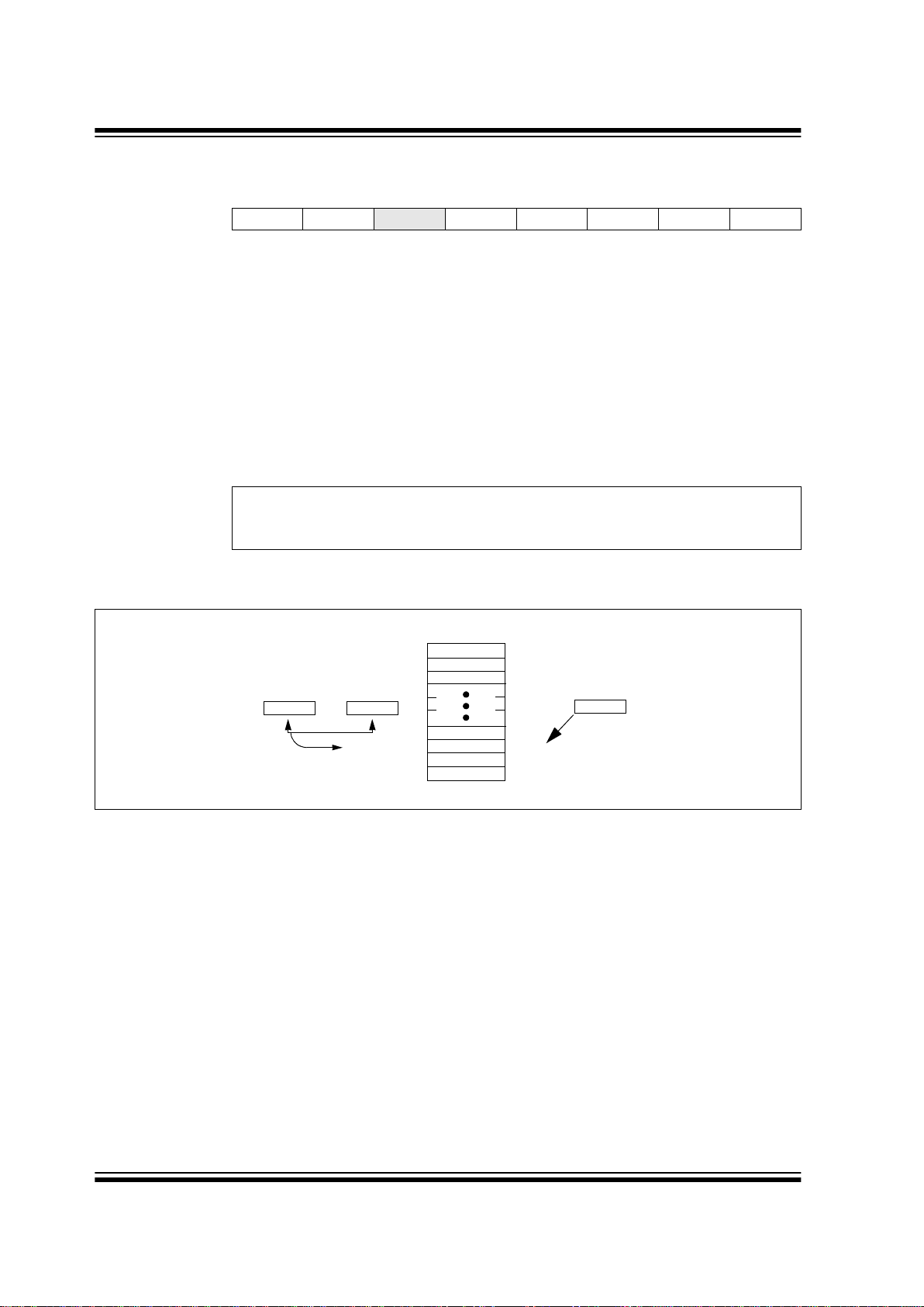
REGISTER 4-1: STKPTR - STACK POINTER REGISTER
FIGURE 4-3: RETURN ADDRESS STACK AND ASSOCIATED REGISTERS
R/C-0 R/C-0 U-0 R/W-0 R/W-0 R/W-0 R/W-0 R/W-0
STKFUL STKUNF
— SP4 SP3 SP2 SP1 SP0
bit7 bit0
bit 7
(1)
STKFUL: Stack Full Flag bit
1 = Stack became full or overflowed
0 = Stack has not become full or overflowed
bit 6
(1)
STKUNF: Stack Underflow Flag bit
1 = Stack underflow occurred
0 = Stack underflow did not occur
bit 5 Unimplemented: Read as ‘0’
bit 4-0 SP4:SP0: Stack Pointer Location bits
Note 1: Bit 7 and bit 6 can only be cleared in user software, or by a POR.
Legend:
R = Readable bit W = Writable bit U = Unimplemented bit, read as ‘0’
- n = Value at POR ’1’ = Bit is set ’0’ = Bit is cleared x = Bit is unknown
00011
0x0A34
11111
11110
11101
00010
00001
00000
00010
Return Address Stack
Top-of-Stack
0x0D58
TOSLTOSH
0x340x1A
STKPTR<4:0>
0x0000

2001 Microchip Technology Inc. Preliminary DS41142A-page 27
PIC18F010/020
4.2.3 PUSH AND POP INSTRUCTIONS
Since the Top-of-Stack (T OS) is readable and writabl e,
the ability to push valu es onto the stack and pull va lues
off the sta ck, withou t disturbi ng normal program exec ution, is a desirable optio n. To push the current PC value
onto the stack, a PUSH instruction can be executed.
This will i ncrem ent th e stack point er and load the cu rrent PC value onto the stack. TOSU, TOSH and TOSL
can then be modified to place a return address on the
stack.
The ability to pull the TOS value off of the stack and
replace it with the value that was previously pushed
onto the stack, without disturbing normal execution, is
achieved by using the POP inst ruction. T he POP instru ction discards the current TOS by decrementing the
stack pointer. The previous value pushed onto the
stack then becomes the TOS value.
4.2.4 STACK FULL/UNDERFLOW RESETS
These RESETS are enabled by programming the
STVREN configuration bit. When the STVREN bit is
disabled, a full or underflow condition will set th e appropriate STKFUL or STKUNF bit, but not cause a device
RESET. When the STVREN bit is enabled, a full or
underflow condition wil l set the appropriate STK FUL or
STKUNF bit and then cause a device RESET. The
STKFUL or STKUNF bits are only cleared by the user
software or a POR Reset.
4.3 Fast Register Stack
A "fast interrupt return " option is available fo r interrupts .
A Fast Register Stack is provided for the STATUS,
WREG and BSR registers and are only one in depth.
The stack is n ot read able o r writ abl e and is lo ade d with
the current value of the corresponding register when
the processor vecto rs for an in terrupt. The va lues in the
registers are then loaded back into the working registers, if th e fast return instruction is used to return
from the interrupt.
A low or high priority interrupt source will push values
into the stack registers. If both low and high priority
interrupts are enabled, the stack registers cannot be
used reliably for low priority interrupts. If a high priority
interrupt occurs while servicing a low priority interrupt,
the stack registe r values stored by the low priority interrupt will be overwritten.
If high priority int errupts are not dis abled during low priority interrupts, users must save the key registers in
software during a low priority interrupt.
If no interrupts are used, the fast register stack can be
used to restore the STATUS, WREG and BSR register s
at the end of a subroutine call. To use the fast register
stack for a subroutine call, a fast call instruction
must be executed.
Example 4-1 sho ws a source code exam ple that uses
the fast register stack.
EXAMPLE 4-1: FAST REGISTER STACK
CODE EXAMPLE
4.4 PCL, PCLATH and PCLATU
The program counter ( PC) spe ci fie s th e ad dre ss of th e
instruction to fetch for execution. The PC is 21-bits
wide. The low byte is called the PCL register. This register is readable and writable. The high byte is called
the PCH register. This register contains the PC<11:8>
bits and is not directly readable or writable. Updates to
the PCH register may be performed through the
PCLATH register. The upper byte is called PCU. This
register contains th e PC<20: 17> bit s an d is not direc tly
readable or writable. Updates to the PCU register may
be performed through the PCLATU register.
The PC addresses bytes in the program memory. To
prevent the PC from becoming misaligned with word
instructions, the LSB of the PCL is fixed to a value of
’0’. The PC increments by 2 to address sequential
instructions in the program memory.
The CALL, RCALL, GOTO and program branch
instructions write to the program counter directly. For
these instructions, the contents of PCLATH and
PCLATU are not transferred to the program counter.
The contents of PCLATH and PCLATU will be transferred to the program counter by an operation that
writes PCL. Similarly, the upper two bytes of the program counter will be transferred to PCLATH and
PCLA TU, by an operation that reads PCL. Thi s is useful
for computed offsets to the PC (see Section4.8.1).
Note: Bits 12 through 16 are not implemented in
the PC and PCLAT.
CALL SUB1, FAST ;STATUS, WREG, BSR
;SAVED IN FAST REGISTER
;STACK
•
•
SUB1 •
•
•
RETURN FAST ;RESTORE VALUES SAVED
;IN FAST REGISTER STACK
PIC18F010/020
DS41142A-page 28 Preliminary 2001 Microchip Technology Inc.
4.5 Clocking Scheme/Instruction
Cycle
The clock input (from OSC1) is internally divided by
four to generate four non-overlapping quadrature
clocks, namely Q1, Q2, Q3 and Q4. Internally, the program counter (PC) is incremented every Q1, the
instruction is fetched from the program memory and
latched into the instruction register in Q4. The instruction is decoded and executed during the following Q1
through Q4. The clocks and instruction execution flow
are shown in Figure4-4.
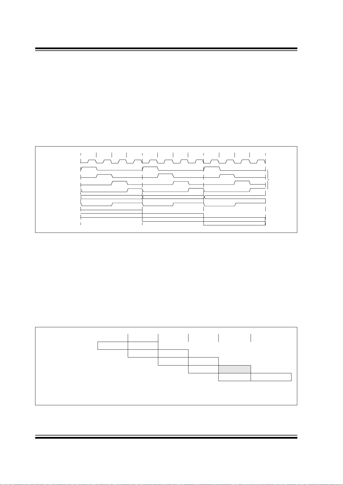
FIGURE 4-4: CLOCK/INSTRUCTION CYCLE
4.6 Instruction Flow/Pipelining
An “Instruction Cycle” consists of four Q cycles (Q1,
Q2, Q3 and Q4). The instruc ti on fe tch and ex ec ute a r e
pipelined su ch that fetch takes one instruction cyc le,
while decode and execute takes another instruction
cycle. However, due to the pipelining, each instruction
effectively executes in one cycle. If an instruction
causes the program counter to change (e.g. GOTO),
then two cycles are re quired to com plete the instruc tion
(Example 4-2).
A fetch cycle begins with the program counter (PC)
incrementing in Q1.
In the execution cy cle, the fetched instruction i s latched
into the “Instruction Register" (IR) in cycle Q1. This
instruction is then decoded and executed during the
Q2, Q3, and Q4 cycles. Dat a memory is read during Q2
(operand read) and written during Q4 (destination
write).
EXAMPLE 4-2: INSTRUCTION PIPELINE FLOW
Q1
Q2 Q3 Q4
Q1
Q2 Q3 Q4
Q1
Q2 Q3 Q4
OSC1
Q1
Q2
Q3
Q4
PC
OSC2/CLKOUT
(Internal Oscillator
PC PC+2 PC+4
Fetch INST (PC)
Execute INST (PC-2) Fetch INST (PC+2)
Execute INST (PC) Fetch INST (PC+4)
Execute INST (PC+2)
Internal
phase
clock
mode)
All instructions are single cycle, except for any program branches. These take two cycles, since the fetch
instruction is “flushed” from the pipeline, while the new instruction is being fetched and then executed.
TCY0TCY1TCY2TCY3TCY4TCY5
1. MOVLW 55h
Fetch 1 Execute 1
2. MOVWF PORTB
Fetch 2 Execute 2
3. BRA SUB_1
Fetch 3 Execute 3
4. BSF PORTA, BIT3 (Forced NOP)
Fetch 4 Flush
5. Instruction @ address SUB_1
Fetch SUB_1 Execute SUB_1

2001 Microchip Technology Inc. Preliminary DS41142A-page 29
PIC18F010/020
4.7 Instructions in Program Memory
The program memory is addressed in bytes. Instructions are stored as two bytes or four bytes in program
memory. The least significant byte of an instruction
word is always stored in a program memory location
with an even address (LSB = ’0’). Figure 4-5 shows an
example of how instructi on words are stored in the program memory. To maintain alignment with instruction
boundaries, the PC increments in steps of 2 and the
LSB will always read ’0’ (see Section 4 .4).
The CALL and GOTO ins tructions have an absol ute program memory address embedded into the instruction.
Since instructions are always stored on word boundaries, the data contained in the instruction is a word
address. The word address is written to PC<20:1>,
which accesses the desired byte address in program
memory. Instruction #2 in Figure 4-5 shows how the
instruction "GOTO 000006h’ is encoded in the program
memory. Program branch instruc tio ns , w hich e nc ode a
relative address offset, operate in the same manner.
The offset value stored in a branch instruction represents the number of single word instructions that the
PC will be offset by. Section 13.0 provides further
details of the instruction set.
FIGURE 4-5: INSTRUCTIONS IN PROGRAM MEMORY
Word Address
LSB = 1 LSB = 0 ↓
Program Memory
Byte Locations
→
000000h
000002h
000004h
000006h
Instruction 1: MOVLW 055h 0Fh 55h 000008h
Instruction 2: GOTO 000006h EFh 03h 00000Ah
F0h 00h 00000Ch
Instruction 3: MOVFF 123h, 456h C1h 23h 00000Eh
F4h 56h 000010h
000012h
000014h

PIC18F010/020
DS41142A-page 30 Preliminary 2001 Microchip Technology Inc.
4.7.1 TWO-WORD INSTRUCTIONS
The PIC18F010/020 devices have 4 two-word instructions: MOVFF, CALL, GOTO and LFSR. The second
word of these instructions has the 4 MSB’s set to 1’s
and is a special kind of NOP instruction. The lower 12
bits of the second word contain data to be used by the
instruction. If the first word of the instruction is executed, the data in the second word is accessed. If the
second word of the in struction is executed by itself (firs t
word was skipped), it will exec ute as a NOP. This action
is necessary when the two-word inst ruction is prec eded
by a conditional in struct ion that cha nges t he PC. A program example tha t demonstrate s this conc ept is show n
in Example 4-3. Refer to Section 13.0 for further deta ils
of the instruction set.
EXAMPLE 4-3: TWO-WORD INSTRUCTIONS
4.8 Lookup Tables
Lookup tables are implemented two ways. These are:
• Computed GOTO
• Table Reads
4.8.1 COMPUTED GOTO
A computed GOTO is accomplish ed b y a dding an offset
to the program counter (ADDWF PCL).
A lookup table can be formed with an ADDWF PCL
instruction and a group of RETLW 0xnn instructions.
WREG is loaded with an o ffset into t he table, befo re executing a call to that table. The fi rst instruction of the c alled
routine is the ADDWF PCL instruction. The next instruction executed will be one of the RETLW 0xnn instructions, that returns the value 0xnn to th e ca llin g fun ctio n.
The offset value (va lue in WREG) specifie s the number
of bytes that the program counter should advance.
In this method, only one data byte may be stored in
each instruction location and room on the return
address stack is required.
4.8.2 TABLE READS/TABLE WRITES
A better method of storing data in program memory
allows 2 bytes of data to be stored in each instruction
location.
Lookup table data may be stored 2 bytes per program
word by using ta ble read s and writes . The t abl e point er
(TBLPTR) specifies the byte address and the table
latch (TABLAT) contains the data that is read from, or
written to, program memo ry. Data is transferred to/from
program memory one byte at a time.
A description of the Table Read/Table Write operation
is shown in Se ction 6.0.
CASE 1:
Object Code Source Code
0110 0110 0000 0000 TSTFSZ REG1 ; is RAM location 0?
1100 0001 0010 0011 MOVFF REG1, REG2 ; No, execute 2-word instruction
1111 0100 0101 0110 ; 2nd operand holds address of REG2
0010 0100 0000 0000 ADDWF REG3 ; continue code
CASE 2:
Object Code Source Code
0110 0110 0000 0000 TSTFSZ REG1 ; is RAM location 0?
1100 0001 0010 0011 MOVFF REG1, REG2 ; Yes
1111 0100 0101 0110 ; 2nd operand becomes NOP
0010 0100 0000 0000 ADDWF REG3 ; continue code

2001 Microchip Technology Inc. Preliminary DS41142A-page 31
PIC18F010/020
4.9 Data Memory Organization
The data memory is impleme nted as st atic RAM . Each
register in the data memory has a 12-bit address,
allowing up to 4096 bytes of data memory. Figure 4-6
and Figure 4-7 show the data memory organization for
the PIC18F010/020 devices.
Banking is required to all ow m ore th an 2 56 b yte s to be
accessed. The data memory map is divided into 2
banks that contai n 25 6 by tes ea ch . The low e r 4 bi t s of
the Bank Select Register (BSR<3:0>) select which
bank will be ac cessed. The upper 4 bits for the BSR
are not impl emented.
The data memory contains Special Function Registers
(SFR) and General Purpose Registers (GPR). The
SFRs are used for control and status of the controller
and peripheral functio ns, while GPRs are us ed for data
storage and scratch pad operations in the user’s application. The SFRs start at the last location of Bank 15
(0xFFF) and grow downwards. GPRs start at the first
location of Bank 0 and grow upwards. Any read of an
unimplemented location will read as ’0’s.
The entire data memory may be accessed directly or
indirectly . Direct ad dressing ma y require t he use of th e
BSR register. Indirect addressing requires the use of
the File Select Register (FSR). Each FSR holds a 12bit address v alue that can be used to access any location in the Data Memory map, without banking.
The instruction set and architecture allow operations
across all banks. This may be accomplished by indirect addressing, or by the u se of the MOVFF instruction.
The MOVFF instruction is a two-word/two-cycle instruction, that moves a value from one register to another.
To ensure that commonly used registers (SFRs and
select GPRs) can be accessed in a single cycle,
regardless of the current BSR values, an Access Bank
is implemented. A segment of Bank 0 and a segment
of Bank 15 comp rise the Access RAM. Section 4.10
provides a detailed description of the Access RAM.
4.9.1 GENERAL PURPOSE REGISTER
FILE
The register file can be ac cess ed eithe r dire ctly o r indirectly. Indirect addressing operates through the File
Select Registers (FSR). The operation of indirect
addressing is shown in Section 4.12.
Enhanced MCU devices may have banked memory in
the GPR area. GPRs are not initialized by a Power-on
Reset and are unchanged on all other RESETs.
Data RAM is available for use as GPR registers by all
instructions. Bank 15 (0xF80 to 0xFFF) co ntains SFRs.
Bank 0 contains GPR registers.
4.9.2 SPECIAL FUNCTION REGISTERS
The Special Function Registers (SFRs) are registers
used by the CPU and Peripheral Modules for controlling the desired operation of the device. These registers are implemented as static RAM. A list of these
registers is given in Figure 4-7 and Figure 4-8.
The SFRs can be classified into two sets: those associated with the “core” function and those related to the
peripheral functions. Those registers related to the
“core” are described in this s ec tio n, while those related
to the operation of the peripheral features are
described in the section of that periphe ral fea t ure.
The SFRs are typica lly d istrib uted a mong the per ipherals whose functions they control.
The unused SFR locations will be unimplemented and
read as '0's. See Figure4-7 for addresses for the
SFRs.
Note: Only 2 banks are implemented, Bank 0 and
Bank 15.

PIC18F010/020
DS41142A-page 32 Preliminary 2001 Microchip Technology Inc.
FIGURE 4-6: DATA MEMORY MAP PIC18F010/020
Bank 0
Bank 14
Bank 15
Data Memory Map
BSR<3:0>
= 0000b
= 0001b
= 1111b
080h
07Fh
F80h
FFFh
00h
7Fh
80h
FFh
Access Bank
When a = 0,
the BSR is ignored and the
Access Bank is used.
The first 128 bytes are
General Purpose RAM
(from Bank 0).
The second 128 bytes are
Special Functio n Reg ist ers
(from Bank 15).
When a = 1,
the BSR is used to specify
the RAM location that the
instructi on uses.
F7Fh
F00h
EFFh
100h
0FFh
000h
Access GPR
FFh
00h
FFh
00h
GPR
Access SFR
SFR
Access SFR
Access GPR
Bank 1
to
Unused
Read ’00h’
= 1110b
= 0010b

2001 Microchip Technology Inc. Preliminary DS41142A-page 33
PIC18F010/020
FIGURE 4-7: SPECIAL FUNCTION REGISTER MAP (F80h-FFFh)
FFFh FDFh INDF2 FBFh F9Fh
FFEh TOSH FDEh POSTINC2 FBEh F9Eh
FFDh TOSL FDDh POSTDEC2 FBDh F9Dh
FFCh STKPTR FDCh PREINC2 FBCh F9Ch reserved
FFBh PCLATU FDBh PLUSW2 FBBh F9Bh OSCTUNE
FFAh PCLATH FDAh FSR2H FBAh F9Ah
FF9h PCL FD9h FSR2L FB9h reserved F99h
FF8h TBLPTRU FD8h STATUS FB8h reserved F98h
FF7h TBLPTRH FD7h TMR0H FB7h reserved F97h
FF6h TBLPTRL FD6h TMR0L FB6h F96h
FF5h TABLAT FD5h T0CON FB5h F95h
FF4h PRODH FD4h reserved FB4h F94h
FF3h PRODL FD3h OSCCON FB3h F93h TRISB
FF2h INTCON FD2h LVDCON FB2h F92h
FF1h INTCON2 FD1h WDTCON FB1h F91h
FF0h INTCON3 FD0h RCON FB0h F90h
FEFh INDF0 FCFh FAFh F8Fh
FEEh POSTINC0 FCEh FAEh F8Eh
FEDh POSTDEC0 FCDh FADh F8Dh
FECh PREINC0 FCCh FACh F8Ch
FEBh PLUSW0 FCBh FABh F8Bh
FEAh FSR0H FCAh FAAh EEADRH F8Ah LATB
FE9h FSR0L FC9h FA9h EEADR F89h
FE8h WREG FC8h FA8h EEDATA F88h
FE7h INDF1 FC7h FA7h EECON2 F87h
FE6h POSTINC1 FC6h FA6h EECON1 F86h
FE5h POSTDEC1 FC5h FA5h F85h
FE4h PREINC1 FC4h FA4h F84h
FE3h PLUSW1 FC3h FA3h F83h
FE2h FSR1H FC2h FA2h IPR2 F82h
FE1h FSR1L FC1h FA1h PIR2 F81h PORTB
FE0h BSR FC0h FA0h PIE2 F80h
Note: Shading indicates addresses within Access Bank. Blank areas indicate reserved register space that may or
may not be implemented in this device.

PIC18F010/020
DS41142A-page 34 Preliminary 2001 Microchip Technology Inc.
FIGURE 4-8: SPECIAL FUNCTION REGISTER MAP (F00h-F7Fh)
F7Fh F5Fh F3Fh F1Fh
F7Eh F5Eh F3Eh F1Eh
F7Dh F5Dh F3Dh F1Dh
F7Ch F5Ch F3Ch F1Ch
F7Bh F5Bh F3Bh F1Bh
F7Ah F5Ah F3Ah F1Ah
F79h WPUB F59h F39h F19h
F78h IOCB F58h F38h F18h
F77h F57h F37h F17h
F76h F56h F36h F16h
F75h F55h F35h F15h
F74h F54h F34h F14h
F73h F53h F33h F13h
F72h F52h F32h F12h
F71h F51h F31h F11h
F70h F50h F30h F10h
F6Fh F4Fh F2Fh F0Fh
F6Eh F4Eh F2Eh F0Eh
F6Dh F4Dh F2Dh F0Dh
F6Ch F4Ch F2Ch F0Ch
F6Bh F4Bh F2Bh F0Bh
F6Ah F4Ah F2Ah F0Ah
F69h F49h F29h F09h
F68h F48h F28h F08h
F67h F47h F27h F07h
F66h F46h F26h F06h
F65h F45h F25h F05h
F64h F44h F24h F04h
F63h F43h F23h F03h
F62h F42h F22h F02h
F61h F41h F21h F01h
F60h F40h F20h F00h
Note: Shading indicates addresses within Access Bank. Blank areas indicate reserved register space that may or
may not be implemented in this device.

2001 Microchip Technology Inc. Preliminary DS41142A-page 35
PIC18F010/020
TABLE 4-1: REGISTER FILE SUMMARY (PIC18F010/020)
File Name Bit 7 Bit 6 Bit 5 Bit 4 Bit 3 Bit 2 Bit 1 Bit 0
Value o n
POR,
BOR
Value on
All Other
RESETS
(Note 1)
FFEh TOSH Top-of-Stack High Byte (TOS<11:8>)
---- 0000 ---- 0000
FFDh TOSL Top-of-Stack Low Byte (TOS<7:0>) 0000 0000 0000 0000
FFCh STKPTR STKOVF STKUNF — Return Stack Pointer 00-0 0000 00-0 0000
FFBh PCLATU — — bit21
(3)
Holding Register for PC<20 :18> — — --00 00-- --00 00--
FFAh PCLATH — — — — Holding Register for PC<11:8> ---- 0000 ---- 0000
FF9h PCL PC Low Byte (PC<7:0>) 0000 0000 0000 0000
FF8h TBLPTRU — — bit21
(2)
Program Memory Table Pointer
Upper Byte (TBLPTR<20:18>)
— — ---0 0000 ---0 0000
FF7h TBLPTRH — — — — Program Memory Table Pointer High Byte
(TBLPTR<11:8>)
0000 0000 0000 0000
FF6h TBLPTRL Program Memory Table Pointer Low Byte (TBLPTR<7:0>) 0000 0000 0000 0000
FF5h TABLAT Program Memory Table Latch 0000 0000 0000 0000
FF4h PRODH Product Register High Byte xxxx xxxx uuuu uuuu
FF3h PRODL Product Register Low Byte xxxx xxxx uuuu uuuu
FF2h INTCON GIE/GIEH PEIE/GIEL T0IE INT0E RBIE T0IF INT0F RBIF 0000 000x 0000 000u
FF1h INTCON2 RBPU INTEDG0 — — — T0IP — RBIP 11-- -1-1 11-- -1-1
FEFh INDF0 Uses contents of FSR0 to address data memory - value of FSR0 not changed (not a physical register) N/A N/A
FEEh POSTINC0 Uses contents of FSR0 to address data memory - value of FSR0 post-incremented (not a physical register) N/A N/A
FEDh POSTDEC0 Uses contents of FSR0 to address data memory - value of FSR0 post-decremented (not a physical register) N/A N/A
FECh PREINC0 Uses contents of FSR0 to address data memory - value of FSR0 pre-incremented (not a physical register) N/A N/A
FEBh PLUSW0 Uses contents of FSR0 to address data memory - value of FSR0 pre-incremented (not a physical register) -
value of FSR0 offset by W
N/A N/A
FEAh FSR0H
— — — — Indirect Data Memory Address Pointer 0 High ---- 0000 ---- 0000
FE9h FSR0L
Indirect Data Memory Address Pointer 0 Low Byte
xxxx xxxx uuuu uuuu
FE8h WREG
Working Register
xxxx xxxx uuuu uuuu
FE7h INDF1
Uses contents of FSR1 to address data memory - value of FSR1 not changed (not a physical register)
N/A N/A
FE6h POSTINC1
Uses contents of FSR1 to address data memory - value of FSR1 post-incremented (not a physical register)
N/A N/A
FE5h POSTDEC1
Uses contents of FSR1 to address data memory - value of FSR1 post-decremented (not a physical register)
N/A N/A
FE4h PREINC1
Uses contents of FSR1 to address data memory - value of FSR1 pre-incremented (not a physical register)
N/A N/A
FE3h PLUSW1
Uses contents of FSR1 to address data memory - value of FSR1 pre-incremented (not a physical register) value of FSR1 offset by W
N/A N/A
FE2h FSR1H
— — — — Indirect Data Memory Address Pointer 1 High
---- 0000 ---- 0000
FE1h FSR1L
Indirect Data Memory Address Pointer 1 Low Byte
xxxx xxxx uuuu uuuu
FE0h BSR
— — — — Bank Select Register
---- 0000 ---- 0000
FDFh INDF2 Uses contents of FSR2 to address data memory - value of FSR2 not changed (not a physical register) N/A N/A
FDEh POSTINC2 Uses contents of FSR2 to address data memory - value of FSR2 post-incremented (not a physical register) N/A N/A
FDDh POSTDEC2 Uses contents of FSR2 to address data memory - value of FSR2 post-decremented (not a physical register) N/A N/A
FDCh PREINC2 Uses contents of FSR2 to address data memory - value of FSR2 pre-incremented (not a physical register) N/A N/A
FDBh PLUSW2 Uses contents of FSR2 to address data memory - value of FSR2 pre-incremented (not a physical register) -
value of FSR2 offset by W
N/A N/A
FDAh FSR2H
— — — — Indirect Data Memory Address Pointer 2 High ---- 0000 ---- 0000
FD9h FSR2L Indirect Data Memory Address Pointer 2 Low Byte xxxx xxxx uuuu uuuu
FD8h STATUS — — — NOVZ DCC---x xxxx ---u uuuu
FD7h TMR0H Timer0 Register High Byte 0000 0000 0000 0000
FD6h TMR0L Timer0 Register Low Byte xxxx xxxx uuuu uuuu
FD5h T0CON TMR0ON T08BIT T0CS T0SE T0PS3 T0PS2 T0PS1 T0PS0 1111 1111 1111 1111
Legend: x = unknown, u = unchanged, - = unimplemented, q = value depends on condition
Note 1: These registers can only be modified when the combination lock is open.

PIC18F010/020
DS41142A-page 36 Preliminary 2001 Microchip Technology Inc.
FD3h OSCCON — IRCF2 IRCF1 IRCF0 OSTO IESO — SCS -000 00-0 -qqq qq-q
FD2h LVDCON — — BGST LVDEN LVV3 LVV2 LVV1 LVV0 --00 0101 --00 0101
FD1h WDTCON — — — — SWP2 SWP1 SWP0 SWDTE ---- 0000 ---- 0000
FD0h RCON IPE — — RI TO PD POR BOR 0--1 11qq 0--q qquu
FB0h PSPCON — — — — — — CMLK1 CMLK0 ---- --00 ---- --00
FA9h EEADR EEPROM Address Register xxxx xxxx uuuu uuuu
FA8h EEDATA EEPROM Data Register xxxx xxxx uuuu uuuu
FA7h EECON2 EEPROM Control Register 2 (not a physical register) ---- ---- ---- ---FA6h EECON1 EEPGD — — FREE WRERR WREN WR RD x--0 x000 u--0 u000
FA2h IPR2 — — — EEIP — LVDIP — — ---1 -1-- ---1 -1--
FA1h PIR2 — — — EEIF — LVDIF — — ---0 -0-- ---0 -0--
FA0h PIE2 — — — EEIE — LVDIE — — ---0 -0-- ---0 -0--
F9Bh OSCTUNE — — TUN5 TUN4 TUN3 TUN2 TUN1 TUN0 --00 0000 --qq qqqq
F93h TRISB — — Data Direction Control Register for PORTB --11 1111 1111 1111
F8Ah LATB — — Read PORTB Data Latch, Write PORTB Data Latch --xx xxxx uuuu uuuu
F81h PORTB — — Read PO RTB pins, Write PORTB Data Latch --xx xxxx uuuu uuuu
F79h WPUB — — WPUB5 WPUB4 WPUB3 WPUB2 WPUB1 WPUB0 --11 1111 0011 1111
F78h IOCB — — IOCB5 IOCB4 IOCB3 IOCB2 IOCB1 IOCB0 --00 0000 0000 0000
Legend: x = unknown, u = unchanged, - = unimplemented, q = value depends on condition
Note 1: These registers can only be modified when the combination lock is open.
TABLE 4-1: REGISTER FILE SUMMARY (PIC18F010/020) (CONTINUED)
File Name Bit 7 Bit 6 Bit 5 Bit 4 Bit 3 Bit 2 Bit 1 Bit 0
Value o n
POR,
BOR
Value on
All Other
RESETS
(Note 1)

2001 Microchip Technology Inc. Preliminary DS41142A-page 37
PIC18F010/020
4.10 Access Bank
The Access Bank is an architectural enhancement
which is very useful for C compiler code optimization.
The techniques used by the C compiler may also be
useful for programs written in assembly.
This data memory region can be used for:
• Intermediate computational values
• Local variables of subroutines
• Faster context saving/switching of variables
• Common variables
• Faster evaluation/control of SFRs (no banking)
The Access Bank is comprised of the upper 128 bytes
in Bank 15 (SFRs) and the lower 128 bytes in Bank 0.
These two sections will be referred to as Access RAM
High and Access RAM Low, respectively. Figure 4-6
and Figure 4-7 indicate the Access RAM areas.
A bit in the instruction word spec ifie s if the opera tion is
to occur in the bank s pecified by t he BSR reg ister, or in
the Access B ank. This bi t is denot ed by the ’a’ bit (for
access bit).
When forced in the Access Bank (a = ’0’), the last
address in Access RAM Low is followed by the first
address in Access RAM High. Access RAM High maps
the Special Function registers, so that these registers
can be accessed without any software overhead. This is
useful for testing status flags and modifying control bits .
4.1 1 Bank Select Register (BSR)
The need for a large general purpose memory space
dictates a RAM banking scheme. The data memory is
partitioned into sixteen banks. When using direct
addressing, the BSR should be configured for the
desired bank.
BSR<3:0> holds the upper 4 bits of the 12-bit RAM
address. The BSR<7:4> bits wil l alw a ys read ’0’s, and
writes will have no effect.
A
MOVLB instruction has been provided in the instruc-
tion set to assist in selecting banks.
If the currently selected bank is not implemented, any
read will return all '0's and all writes are ignored. The
ST ATUS register bits will be set/c le ared as ap prop ria te
for the instruction performed.
Each Bank extends up to FFh (256 bytes). All data
memory is implemented as static RAM.
A MOVFF instr uctio n igno res t he BSR, sinc e the 12-bit
addresses are embedded into the instruction word.
Section 4.12 provides a description of indirect a ddressing, which allows linear addressing of the entire RAM
space.
FIGURE 4-9: DIRECT ADDRESSING
Note 1: For register file map detail, see Table 4-7.
2: The access bit of the instruction can be used to force an override of the select ed bank (B SR<3: 0>) to the
registers of the Access Bank.
3: The
MOVFF instruction embeds the entire 12-bit address in the instruction.
Data
Memory
(1)
Direct Addressing
Bank Select
(2)
Location Select
(3)
BSR<3:0> 7
0
From Opcode
(3)
00h 01h 0Eh 0Fh
Bank 0 Bank 1 Bank 14 Bank 15
1FFh
100h
0FFh
000h
EFFh
E00h
FFFh
F00h

PIC18F010/020
DS41142A-page 38 Preliminary 2001 Microchip Technology Inc.
4.12 Indirect Addressing, INDF and
FSR Registers
Indirect addressing is a mode of addressing dat a memory, where the data memory address in the instruction
is not fixed. An SFR regis ter i s u sed as a poi nte r to the
data memory location that i s to be read or wr itten. Since
this pointer is in RAM, the con tents can be modified by
the program. This can be useful for data tables in the
data memory and for software stacks. Figure 4-10
shows the operation of indirect addressing. This shows
the moving of the value to the data memory address
specified by the value of the FSR register.
Indirect addressing is possible by using one of the INDF
registers. Any instruction using the INDF register actually accesses the register pointed to by the File Select
Register, FSR. Reading the INDF register itself indirectly
(FSR = ’0’) will read 00h. Writing to the INDF register
indirectly results in a no-operation. The FSR register
contains a 12-bit address, which is shown in Figure 4-
10.
The INDFn register is not a physical register. Addressing INDFn actually addresses the register whose
address is contained in the FSRn register (FSRn is a
pointer). This is indire ct addressing.
There are three indirect addressing registers. To
address the entire data memory space (4096 bytes),
these registers are 12-bit wide. To store the 12-bits of
addressing information, two 8-bit registers are
required. These indirect addres si ng regi ste rs are:
1. FSR0: composed of FSR0H:FSR0L
2. FSR1: composed of FSR1H:FSR1L
3. FSR2: composed of FSR2H:FSR2L
In addition, there are registers INDF0, INDF1 and
INDF2, which are not physically implemented. Reading
or writing to these registers activates indirect addressing, with the value in the corresponding FSR register
being the address of the data.
If an instruction writes a value to INDF0, the value will
be written to the address pointed to by F S R0H :FSR0 L.
A read from INDF1, reads the data from the address
pointed to by FSR1H:FS R1L. INDFn can be used in
code anywhere an operand can be used.
If INDF0, INDF1, or INDF2 are read indirectly via an
FSR, all ’0’s are read (zero bit is set). Similarly, if
INDF0, INDF1, or INDF2 are written to indirectly, the
operation will be equivale nt to a NOP instruction an d the
STATUS bits are not affected.
4.12.1 INDIRECT ADDRESSING
OPERATION
Each FSR register has an INDF register associated
with it, plus four additional reg ister addresses. Perform ing an operation on one of these five registers determines how the FSR will be modified during indirect
addressing.
When data access is done to one of the five INDFn
locations, the address selected will configure the FSRn
register to:
• Do nothing to FSRn after an indirect access (no
change) - INDFn
• Auto-decrement FSRn after an indirect access
(post-decrement) - POSTDECn
• Auto-increment FSRn after an indirect access
(post-increment) - POSTINCn
• Auto-increment FSRn before an indirect access
(pre-increment) - PREINCn
• Use the signed value of WREG as an offset to
FSRn. Do not modify the value of the WREG or
the FSRn register after an indirect access (no
change) - PLUSWn
When using the auto-increment or auto-decrement features, the effect on the FSR i s not refl ec ted in the STATUS register. For example, if the indirect address
causes the FSR to equal '0', the Z bit will not be set.
Incrementing or decrementing an FSR affects all 12
bits. That is, whe n FSRnL overflows from an increment,
FSRnH will be incremented automatically.
Adding these features allows the FSRn to be used as a
stack pointer, in addition to its uses for table operations
in data memory.
Each FSR has an address associated with it that performs an indexed indirect access. When a data access
to this INDFn location (PLUSWn) occurs, the FSRn is
configured to add th e s ig ned v alu e in the WR EG re gis ter and the value in F SR to f orm the add res s befo re a n
indirect access. The FSR value is not changed.
If an FSR register contains a value that point s to one of
the INDFn, an indirect read will read 00h (zero bit is
set), while an i ndi rect wri te will be equ ival ent t o a NOP
(ST ATUS bits are not affected).
If an indirect addressing operation is done where the
target address is an FSRnH or FSRnL register, the
write operation will dominate over the pre- or postincrement /decrement functions.

2001 Microchip Technology Inc. Preliminary DS41142A-page 39
PIC18F010/020
FIGURE 4-10: INDIRECT ADDRESSING
Note 1: For register file map detail, see Table 4-7.
Data
Memory
(1)
Indirect Addressing
FSR Register11
0
0FFFh
0000h
Location Select

PIC18F010/020
DS41142A-page 40 Preliminary 2001 Microchip Technology Inc.
4.13 STATUS Register
The STATUS register, shown in Register4-2, contains
the arithmetic status of the ALU. The STATUS register
can be the destination for any instruction, as with any
other register. If the STATUS register is the destination
for an instruction that affect s the Z, DC, C, OV, or N bits,
then the write to these five bits is disabled. These bits
are set or cleare d a ccord ing to the device logi c. The r efore, the result of a n ins tructi on with the STATUS register as destination may be different than intended.
For example, CLRF STATUS will clear the upper three
bits and set the Z bit. T his leaves the STATUS regist er
as 000u u1uu (where u = unchanged).
It is recommended, therefore, that only BCF, BSF,
SWAPF, MOVFF and MOVWF instructions are used to
alter the STATUS regis ter, because these i nstruc tions
do not affect the Z, C, DC, OV or N bits from the ST ATUS register. For other instructions not affecting any
status bits, see Table 13-2.
REGISTER 4-2: STATUS REGISTER
Note: The C and DC bits operate as a borrow and
digit borrow
bit respectively, in subtraction.
U-0 U-0 U-0 R/W-x R/W-x R/W-x R/W-x R/W-x
— — — NOVZDCC
bit 7 bit 0
bit 7-5 Unimplemented: Read as '0'
bit 4 N: Negative bit
This bit is used for signed arithmetic (2’s complement). It indicates whether the result was
negative, (ALU MSB = 1).
1 = Result was negative
0 = Result was positive
bit 3 OV: Overflow bit
This bit is used for signed arithmetic (2’s complement). It indicates an overflow of the 7-bit
magnitude, which causes the sign bit (bit 7) to change state.
1 = Overflow occurred for signed arithmetic (in this arithmetic operation)
0 = No overflow occurred
bit 2 Z: Zero bit
1 = The result of an arithmetic or logic operation is zero
0 = The result of an arithmetic or logic operation is not zero
bit 1 DC: Digit carry/borrow
bit
For ADDWF, ADDLW, SUBLW, and SUBWF instructions
1 = A carry-out from the 4th low order bit of the result occurred
0 = No carry-out from the 4th low order bit of the result
Note: For borrow,
the polarity is reversed. A subtraction is executed by adding the two’s
complement of the second operand. For rotate (RRF, RLF) instructions, this bit is
loaded with either the bit 4 or bit 3 of the source register.
bit 0 C: Carry/borrow bit
For ADDWF, ADDLW, SUBLW, and SUBWF instructions
1 = A carry-out from the most significant bit of the result occurred
0 = No carry-out from the most significant bit of the result occurred
Note: For borrow,
the polarity is reversed. A subtraction is executed by adding the two’s
complement of the second operand. For rotate (RRF, RLF) instructions, this bit is
loaded with either the high or low order bit of the source register.
Legend:
R = Readable bit W = Writable bit U = Unimplemented bit, read as ‘0’
- n = Value at POR ’1’ = Bit is set ’0’ = Bit is cleared x = Bit is unknown

2001 Microchip Technology Inc. Preliminary DS41142A-page 41
PIC18F010/020
4.14 RCON Register
The RESET Control (RCON) register contains flag bits,
that allow differentiation between the sources of a
device RESET. These flags incl ude the TO
, PD, POR,
BOR
and RI bits. This regis ter is rea dable and writabl e.
REGISTER 4-3: RCON REGISTER
Note 1: If the BOREN configuration bit is set,
BOR
is ’1’ on Power-on Reset. If the
BOREN configuration bit is clear, BOR
is
unknown on Power-on Reset.
The BOR
status bit is a "don't care" and is
not necessarily predictable if the brownout circuit is disabled (th e BOR EN co nfi guration bit is clear). BOR
must then be set
by the user and checked on subsequent
RESETS to see if it is clear, indicating a
brown-out has occurred.
2: It is recomm ended that the POR
bit be set
after a Power-on Reset has been
detected, so that subsequent Power-on
Resets may be detected.
R/W-0 U-0 U-0 R/W-1 R-1 R-1 R/W-0 R/W-0
IPEN — — RI TO PD POR BOR
bit 7 bit 0
bit 7 IPEN: Interrupt Priority Enable bit
1 = Enable priority levels on interrupts
0 = Disable priority levels on interrupts (16CXXX compatibility mode)
bit 6-5 Unimplemented: Read as ‘0’
bit 4 RI
: RESET Instruction Flag bit
1 =The RESET instruction was not executed
0 =The RESET instruction was executed causing a device RESET
(must be set in software after a Brown-out Reset occurs)
bit 3 TO
: Watchdog Time-out Flag bit
1 = After power-up, CLRWDT instruction, or SLEEP instruction
0 = A WDT time-out occurred
bit 2 PD
: Power-down Detection Flag bit
1 = After power-up or by the CLRWDT instruction
0 = By execution of the SLEEP instruction
bit 1 POR
: Power-on Reset Status bit
1 = A Power-on Reset has not occurred
0 = A Power-on Reset occurred
(must be set in software after a Power-on Reset occurs)
bit 0 BOR
: Brown-out Reset Status bit
1 = A Brown-out Reset has not occurred
0 = A Brown-out Reset occurred
(must be set in software after a Brown-out Reset occurs)
Legend:
R = Readable bit W = Writable bit U = Unimplemented bit, read as ‘0’
- n = Value at POR ’1’ = Bit is set ’0’ = Bit is cleared x = Bit is unknown

PIC18F010/020
DS41142A-page 42 Preliminary 2001 Microchip Technology Inc.
NOTES:

2001 Microchip Technology Inc. Preliminary DS41142A-page 43
PIC18F010/020
5.0 DATA EEPROM MEMORY
The Data EEPROM is readable and writable during
normal operation (full V
DD range). Thi s memor y is no t
directly mapped in the register file space. Instead, it is
indirectly address ed throug h the Special Function Registers. There are four SFRs used to read and write this
memory. These registers are:
• EECON1 (0FA6h)
• EECON2 (0FA7h)
• EEDATA (0FA8h)
• EEADR (0FA9h)
When interfacing the data memory block, EEDATA
holds the 8-bit data for read/write, and EEADR holds
the address of the EEPROM location being accessed.
These devices have 64 bytes of da ta EEPROM with an
address range from 0h to 03Fh.
The EEPROM data memory allows byte read and write.
A byte write automatically erases the location and
writes the new data (erase before write).
The EEPROM data memory is rated for high erase/
write cycles. Th e wr it e ti me is c ont rolled by an on-chip
timer . The write time wi ll vary with volt age and temperature, as well as from chip-to-chip. Please refer to the
specifications for exact limits.
When the device is code protec ted, the CPU may continue to read and write the data EEPROM memory.
5.1 EEADR
The EEADR register can address up to a maximum of
256 bytes of data.
When the device contains less memory than the full
address reach of the EEADR register, the MSb’s of the
register must be set to ‘0’. For example, this de vice ha s
64 bytes of data EE, the Most Significant 2 bits of the
register must be ‘0’.
5.2 EECON1 and EECON2 Registers
EECON1 is the control register for memory accesses.
EECON2 is not a physical register. Reading EECON2
will read all '0's. The EECON2 register is used
exclusively in the memory write sequence.
Control bit EEPGD determines if the access will be a
program or a data memory access. When clear, any
subsequent operations will operate on the data memory . When s et, an y subsequ ent operat ions will opera te
on the program memory.
Control bits RD and WR initiate read and write operations, respectively. These bits cannot be cleared, only
set, in software. They are cleared in hardware at the
completion of the read or write operation. The inability
to clear th e WR bi t i n so ftwa r e pre v en ts th e ac ci d en tal
or premature termination of a write operation.
The WREN bit, when set, will allow a write operation.
On power-up, the WREN bit is c lear . Th e WRERR bi t is
set when a write operation is interrupted by a MCLR
Reset, or a WDT Time-out Reset, during normal operation. In these situations, following RESET, the user
can check the WRERR bit and rewr ite the location. Th e
value of the data and address registers and the
EEPGD bit remains unchanged.
Interrupt flag bit EEIF in the PIR2 register, is set when
a write is complete. It must be cleared in software.

PIC18F010/020
DS41142A-page 44 Preliminary 2001 Microchip Technology Inc.
REGISTER 5-1: EECON1 REGISTER (ADDRESS 18Ch)
R/W-U U-0 U-0 R/W-0 R/W-x R/W-0 R/S-0 R/S-0
EEPGD
— — FREE WRERR WREN WR RD
bit 7 bit 0
bit 7 EEPGD: FLASH Program or Data EEPROM Memory Select bit
1 = Access Program FLASH memory
0 = Access Data EEPROM memory
bit 6-5 Unimplemented: Read as ‘0’
bit 4 FREE: FLASH Row Erase Enable bit
1 = Erase the row addressed by TBLPTR on the next WR command (reset by hardware)
0 = Perform write only
bit 3 WRERR: EEPROM Error Flag bit
1 = A write operation is prematurely terminated
(any MCLR
Reset or any WDT Reset during normal operation)
0 = The write operation completed
bit 2 WREN: EEPROM Write Enable bit
1 = Allows write cycles
0 = Inhibits write to the EEPROM
bit 1 WR: Write Control bit
1 = Initiates a write cycle. (The bit is cleared by hardware once write is complete. The WR
bit can only be set (not cleared) in software.)
0 = Write cycle to the EEPROM is complete
bit 0 RD: Read Control bit
1 = Initiates an EEPROM read. (Read takes one cycle. RD is cleared in hardware. The RD
bit can only be set (not cleared) in software.)
0 = Does not initiate an EEPROM read
Legend:
R = Readable bit W = Writable bit U = Unimplemented bit, read as ‘0’
- n = Value at POR ’1’ = Bit is set ’0’ = Bit is cleared x = Bit is unknown

2001 Microchip Technology Inc. Preliminary DS41142A-page 45
PIC18F010/020
5.3 Reading the Data EEPROM
Memory
T o read a d ata memory loca tion, the user must write the
address to the EEADR register, clear the EEPGD control bit (EECON1<7>), and then set control bit RD
(EECON1<0>). The data is available in the very next
instruction cycle of the EEDATA register, therefore, it
can be read by the next instruction. EEDATA will hold
this value until another read operation or until it is written to by the user (during a write operation).
EXAMPLE 5-1: DATA EEPROM READ
MOVLW DATA_EE_ADDR ;
MOVWF EEADR ;Data Memory Address to read
BCF EECON1, EEPGD ;Point to DATA memory
BSF EECON1, RD ;EEPROM Read
MOVF EEDATA, W ;W = EEDATA
5.4 Writing to the Data EEPROM
Memory
To write an EEPROM data location, the address must
first be written to the EEADR r egiste r and the da ta written to the EEDATA register. Then the sequence in
Example 5-2 must be followed to initiate the write cycle.
EXAMPLE 5-2: DATA EEPROM WRITE
The write will not i nitiate if the above r equired seque nce
is not exactly followed (write 55h to EECON2, write
AAh to EECON2, then set WR bit) for each byte. It is
strongly recommended that interrupts be disabled during this code segment.
Additionally, the WREN bit in EECON1 must be set to
enable writes. This mechanism prevents accidental
writes to data EEPROM due to unexpected code execution (i.e., runaway programs). The WREN bit should
be kept clear at all times, except when updating the
EEPROM. The WREN bit is not cleared byhardware
After a write sequence has been initiated, clearing the
WREN bit will not aff ect the current write cy cle. The WR
bit will be inhibited from being set unless the WREN bit
is set. The WREN bit must be set on a previous ins truction. Both WR and WREN c an not be set with the same
instruction.
At the completion of the write cycle, the WR bit is
cleared in hardware and th e EEPROM Write Complete
Interrupt Flag bit (EEIF) is set. EEIF must be cleared b y
software.
Note: Do not write to program memory or
EECON1 while writing to EEDATA.
MOVLW DATA_EE_ADDR ;
MOVWF EEADR ; Data Memory
Address to write
MOVLW DATA_EE_DATA ;
MOVWF EEDATA ; Data Memory
Value to write
BCF EECON1, EEPGD ; Point to DATA
memory
BSF EECON1, WREN ; Enable writes
BCF INTCON, GIE ; Disable
Interrupts
MOVLW 55h ;
Required MOVWF EECON2 ; Write 55h
Sequence MOVLW AAh ;
MOVWF EECON2 ; Write AAh
BSF EECON1, WR ; Set WR bit to
begin write
BSF INTCON, GIE ; Enable
Interrupts
SLEEP ; Wait for
interrupt to
signal write
complete
BCF EECON1, WREN ; Disable writes

PIC18F010/020
DS41142A-page 46 Preliminary 2001 Microchip Technology Inc.
5.5 Protection Against Spurious W rite
5.5.1 EEPROM DATA MEMORY
There are conditions when the device may not want to
write to the data EEPROM memory. To protect against
spurious EEPROM writes, various mechanisms have
been built -in. On powe r-up, the WR EN bit is cl eared.
Also, the Power-up Timer (72 ms duration) prevents
EEPROM write.
The write initiate se que nc e an d the WR EN bit together
help prevent an accidental write during brown-out,
power glitch, or software malfunction.
5.6 Operation During Code Protect
Each reprogrammable m emory b lo ck has it s own code
protect mechanism. External Read and Write operations are dis abled if either of th ese mechanisms are
enabled.
5.6.1 DATA EEPROM MEMORY
The microcontroller i tself c an both re ad and wr ite to the
internal Data EEPROM, regardless of the state of the
code protect configuration bit.
TABLE 5-1: REGISTERS ASSOCIATED WITH DATA EEPROM/PROGRAM FLASH
Address Name Bit 7 Bit 6 Bit 5 Bit 4 Bit 3 Bit 2 Bit 1 Bit 0
Value on :
POR,
BOR
Value on
all other
RESETS
FA9h EEADR EEPROM Address Register
xxxx xxxx uuuu uuuu
FA8h EEDATA EEPROM Data Register xxxx xxxx uuuu uuuu
FA7h EECON2 EEPROM Control Register2 (not a physical register) ---- ---- ---- ---FA6h EECON1 EEPGD — — FREE WRERR WREN WR RD x--0 x000 u--0 u000
FA2h IPR2 — — — EEIP — LVDIP — — ---1 1--- ---1 1---
FA1h PIR2 — — — EEIF — LVDIF — — ---0 0--- ---0 0---
FA0h PIE2 — — — EEIE — LVDIE — — ---0 0--- ---0 0---
FF2h INTCON GIE/GIEH PEIE/GIEL T0IE INT0IE RBIE T0IF INT0F RBIF 0000 000x 0000 000u
Legend: x = unknown, u = unchanged, r = reserved, - = unimplemented, read as '0'.
Shaded cells are not used during FLASH/EEPROM access.
Note 1: These bits are reserved; always maintain these bits clear.

2001 Microchip Technology Inc. Preliminary DS41142A-page 47
PIC18F010/020
6.0 TABLE READ/WRITE
INSTRUCTIONS
The PIC18F010/020 has eight instructions that allow
the processor to move data from the data memory
space to the program memory space, and vice versa.
These eight instructions manipulate the Table Pointer
in a manner similar to the FSR’s.
The TBLRD instructions are used to read dat a from the
program memory space to the data memory space.
The TBLWT instructions are used to write data from the
data memory space to the program memory space.
6.1 Control Registers
A few control registers are used in conjunction with the
TBLRD and TBLWT instructions. These include the:
• EECON1 register
• TABLAT register
• TBLPTR registers
6.1.1 EECON1 REGISTER
The EECON1 register holds bits to control erase and
write operations in FLASH memory. The EEPGD bit
selects data EEPROM, if clear, or program FLASH
memory, if set. The FREE bit is used to select erasing
versus writ ing to FLA SH. The WR EN bit enab les wr iting. Finally, the WRERR bit indicates any errors. Refer
to Register 5-1 for details.
6.2 T able Reads from FLASH Program
Memory
Table Reads from program memory are perform ed on e
byte at a time. The in struction will access one byte from
the program memory pointed to by the TBLPTR and
transfer that byte to the TABLAT. Figure 6-1 diagrams
the Table Read operation.
The TBLPTR can be updated in one of four ways,
based on the Table Read instructions:
• TBLRD* no-change
• TBLRD*+ post-increment
• TBLRD*- post-decrement
• TBLRD+* pre-increment
The internal program memo ry is normally word wide.
The Least Significant bit of the address selects between
the high and low bytes of the word. Fi gure 6-2 shows
the typical interface between the internal program
memory and the TABLAT.
FIGURE 6-1: TBLRD* INSTRUCTION OPERATION
Table Pointer
Table Latch (8-bit)
Program Memory
TBLPTRH
TBLPTRL
TABLAT
Prog-Mem
(TBLPTR)
TBLPTRU
Instruction: TBLRD*

PIC18F010/020
DS41142A-page 48 Preliminary 2001 Microchip Technology Inc.
EXAMPLE 6-1: PROGRAM MEMORY
READ
MOVLW CODE_ADDR_UPPER; Load TBLPTR
; Register
MOVWF TBLPTRU ; with Address to
; Read
MOVLW CODE_ADDR_HIGH ;
MOVWF TBLPTRH ;
MOVLW CODE_ADDR_LOW ;
MOVWF TBLPTRL ;
TBLRD* ; Read Memory
MOVF TABLAT,W ; W = Data
FIGURE 6-2: TABLE READS / WRITES TO INTERNAL PROGRAM MEMORY
Buffer Register
TABLAT Write Reg.
Program Memory
Bank 1
(Odd Address)
Program Memory
Bank 0
(Even Address)
TBLWT
* A0=1
TBLWT
* A0=1
TBLWT
*
A0=1
TBLRD
TABLAT Read Reg.
Buffer Register
TBLWT *
*
A0=0
A0=1 A0=0
FLASH word write
done when
TBLWT to
address with A0=1

2001 Microchip Technology Inc. Preliminary DS41142A-page 49
PIC18F010/020
6.3 Erasing FLASH Program Memory
Word erase in the FLASH array is not supported. The
minimum erase block is one row of a panel, which is
equivalent to 16 words or 32 bytes.
Erase operations may be commanded from one of two
sources. Under us er program co ntrol, the minim um one
row of memory is erased. Under programmer or
ICSP
TM
control, larger blocks of program memory may
be bulk erased.
6.3.1 ERASING FLASH PROGRAM
MEMORY IN OPERATIONAL MODE
In normal mode, a block of 32 bytes of program memory is erased. The Most Significant 16 bits of the
TBLPTR<21:6> points to the block being erased.
TBLPTR<4:0> are ignored.
The EECON1 register commands the era se opera tio n.
The EEPGD bit must be set to point to the FLASH program memory. The WREN bit must be set to enable
write operations. The F REE bit is set to select an erase
operation.
For protecti on, the writ e initiate sequence for EECON2
must be used. When the WR bit is set, a long write is necessary for erasin g the internal F LASH. Instruc tion execution is halted while in a long write cycle. The long write will
be terminated by the internal programming timer. Instruction execution will resume with no lost instructions.
The sequence of events for erasing a block of internal
program memory location is:
1. Load Table Pointer with address of row being
erased.
2. Set FREE bit to enable row erase; set WREN bit
to enable writes and set EEPGD bit to point to
program memory.
3. Disable interrupts.
4. Write ’55’ to EECON2.
5. Write 'AA’ to EECON2.
6. Set the WR bit. This will begin the row erase cycle.
7. CPU will stall for duration of the erase (about
2ms using internal timer).
6.4 FLASH Array Programming
Operations
Word or byte programming is not supported. The minimum programming block is 32-bits or 2 words.
6.4.1 PROGRAM MING FL ASH PR OGRAM
MEMORY IN OPERATIONAL MODE
(TABLE LONG WRITES)
Conceptually, Tabl e Wri tes are pe rformed one b yte at a
time. The instructi on will write one byte cont ained in the
TABLAT register to the internal memory, pointed to by
the TBLPTR, as shown in Figure 6-3.
The TBLPTR can be updated in one of four ways,
based on the Table Write instructions:
• TBLWT* no-change
• TBLWT*+ post-increment
• TBLWT*- post-decrement
• TBLWT+* pre-increment
The program memory FLASH uses a similar mechanism to the data EEPROM. Table Writes are used int ernally to load the Write registers used to program the
FLASH memory . The EECON1 registe r is used to actually command a write or erase event.
Each FLASH panel is programmed with 32 of 256 columns
at a time. This translates into 32 write bit latches. These
write latches are accessed using Table Write instructions,
which can write a byte at a time. There are then 4 Table
Writes require d to wri te t he latche s for o ne p anel .
Since the table latch is only a single byte, the TBLWT
instruction has to be executed 4 times for each programming operation. All of the Table Write operations
will essentially be short writes, because only the table
latches are written. At the end of updating 4 l atches, the
EECON1 register must be written to start the programming operation with a long write.
The long write is necessary for programming the internal FLASH. Instruction execution is halted while in a
long write cycle. The long write will be terminated by
the internal programming timer. Instruction execution
will resume with two lost instructions.
The write time is controlled by the EEPROM on-chip
timer . The write/er ase voltages are generated by an onchip charge pump, rated to operate over the voltage
range of the device for byte or word operations. When
doing block oper ations, the de vice must be operatin g in
the 5V ±10% range.
Note: When writing a block, insure the table
pointer is pointing to t he desired blo ck after
the last short write.
The first and second instruction following
the TBLWT must be NOPs.

PIC18F010/020
DS41142A-page 50 Preliminary 2001 Microchip Technology Inc.
The sequence of events for programming an internal
program memory location should be:
1. Read 32 bytes of row into RAM.
2. Update data values in RAM, as necessary.
3. Load Table Pointer with address of row being
erased.
4. Perform the row erase procedure.
5. CPU will stall for duration of the erase (about
2ms using internal timer).
6. Load T able Pointer wit h address first by te of row
being written.
7. Set WREN bit to enable writes and set EEPGD
bit to point to program memory.
8. Write first 3 bytes into table latches with autoincrement. Write the last byte without autoincrement.
9. Disable interrupts.
10. Write ’55’ to EECON2.
11. Write 'AA’ to EECON2.
12. Se t the WR bit. This will beg in the w rite cy cl e.
13. CPU wil l stall for duration of the write (about 2ms
using internal timer).
14. Repeat steps 7-13, 8 times total to write 32
bytes.
15. Verify the memory row (Table Read).
This procedure will require about 18msec to update 1
row of 32 bytes of memory.
FIGURE 6-3: TABLE W RITES TO INTERNAL PROGRAM MEMORY
Buffer Register
TABLAT Write Reg.
Program Memory
(Column 0-7)
TBLWT
A=xxxxx1
Buffer Register
TBLWT
A=xxxxx0
Buffer Register
TBLWT
A=xxxxx2
Buffer Register
TBLWT
A=xxxxx3
(Column 8-15)(Column 16-23)(Column 24-31)

2001 Microchip Technology Inc. Preliminary DS41142A-page 51
PIC18F010/020
EXAMPLE 6-2: PROGRAM MEMORY WRITE
This example will bu ffer a segme nt of memory , m odify one word in the buffer , erase the segment row , and w rite the buff er
back to memory.
MOVLW 32 ; number of bytes in row
MOVWF COUNTER
MOVLW BUFFER_ADDR_HIGH ; point to buffer
MOVWF FSR0H
MOVLW BUFFER_ADDR_LOW ;
MOVWF FSR0L
MOVLW CODE_ADDR_UPPER ; Load TBLPTR with the base
MOVWF TBLPTRU ; address of the memory row
MOVLW CODE_ADDR_HIGH ;
MOVWF TBLPTRH ;
MOVLW CODE_ADDR_LOW ;
MOVWF TBLPTRL ;
READ_ROW
TBLRD*+ ; read into TABLAT, and inc
MOVF TABLAT, W ; get data
MOVWF POSTINC0 ; store data
DECFSZ COUNTER ; done?
GOTO READ_ROW ; repeat
MODIFY_WORD
MOVLW DATA_ADDR_HIGH ; point to buffer
MOVWF FSR0H
MOVLW DATA_ADDR_LOW ;
MOVWF FSR0L
MOVLW NEW_DATA_LOW ; update buffer word
MOVWF POSTINC0
MOVLW NEW_DATA_HIGH
MOVWF INDF0
ERASE_ROW
MOVLW CODE_ADDR_UPPER ; Load TBLPTR with the base
MOVWF TBLPTRU ; address of the memory row
MOVLW CODE_ADDR_HIGH ;
MOVWF TBLPTRH ;
MOVLW CODE_ADDR_LOW ;
MOVWF TBLPTRL ;
BSF EECON1,WREN ; enable write to memory
BSF EECON1,FREE ; Enable Row Erase operation
BSF EECON1,EEPGD ; Point to FLASH program memory
MOVLW 55h
MOVWF EECON2 ; write 55H
MOVLW AAh
MOVWF EECON2 ; write AAH
BSF EECON1,WR ; start erase (CPU stall)
WRITE_BUFFER_BACK
MOVLW 8 ; number of write buffer groups of 4 bytes
MOVWF COUNTER_HI
MOVLW BUFFER_ADDR_HIGH ; point to buffer
MOVWF FSR0H
MOVLW BUFFER_ADDR_LOW ;
MOVWF FSR0L
TBLRD*- ; back the TBLPTR up one
PROGRAM_LOOP
MOVLW 4 ; number of bytes in write buffer
MOVWF COUNTER

PIC18F010/020
DS41142A-page 52 Preliminary 2001 Microchip Technology Inc.
EXAMPLE 6-2: PROGRAM MEMORY WRITE (CONTINUED)
WRITE_WORD_TO_BUFFERS
MOVF POSTINC0, W ; get low byte of buffer data
MOVWF TABLAT ; present data to table latch
TBLWT+* ; write data, perform a short write to pre-increment and load data to
NOP ; internal TBLWT holding register.
NOP ; loop until buffers are full
DECFSZ COUNTER
GOTO WRITE_WORD_TO_BUFFERS
PROGRAM_MEMORY
BSF EECON1,WREN ; enable write to memory
BSF EECON1,EEPGD ; Point to FLASH program memory
MOVLW 55h
MOVWF EECON2 ; write 55H
MOVLW AAh
MOVWF EECON2 ; write AAH
BSF EECON1,WR ; start program (CPU stall)
DECFSZ COUNTER_HI ; loop until done
GOTO PROGRAM_LOOP
BCF EECON1,WREN ; disable write to memory

2001 Microchip Technology Inc. Preliminary DS41142A-page 53
PIC18F010/020
6.4.2 TABLAT - TABLE LATCH REGISTER
The Table Latch (TABLAT) is an 8-bit register mapped
into the SFR space. The Table Latch is used to hold 8bit data during data transfers between program memory and data memory.
6.4.3 TBLPTR - TABLE POINTER
REGISTER
The Table Pointer (TBLPTR) addresses a byte within
the program memory. The TBLPTR is comprised of
three SFR registers (Table Pointer Upper byte, High
byte and Low byte). These three registers
(TBLPTRU:TBLPTRH:TBLPTRL) join to form a 22-bit
wide pointer. The low order 21-bits allow the device to
address up to 2 Mbytes of p rogram memory sp ace. The
22nd bit allows access to the Device ID, the User ID
and the Configuration bits.
The table po inter TB LPTR is used by the TBLRD and
TBLWT instructions. These instructions can update the
TBLPTR in one of four ways, based on the table operation. These opera tion s a re s ho w n in Table 6-1. These
operations on the TBLPTR only affect the low order
21-bits.
TABLE 6-1: TABLE POINTER OPERATIONS WITH TBLRD AND TBLWT INSTRUCTIONS
Example Operation on Table Pointer
TBLRD*
TBLWT*
TBLPTR is not modified
TBLRD*+
TBLWT*+
TBLPTR is incremented after the read/write
TBLRD*TBLWT*-
TBLPTR is decr emented after the read/write
TBLRD+*
TBLWT+*
TBLPTR is incremented before the read/write

PIC18F010/020
DS41142A-page 54 Preliminary 2001 Microchip Technology Inc.
NOTES:

2001 Microchip Technology Inc. Preliminary DS41142A-page 55
PIC18F010/020
7.0 8 X 8 HARDWARE MULTIPLIER
7.1 Introduction
An 8 x 8 hardware multiplier is included in the ALU of
the PIC18F010/020 devices. By making the multiply a
hardware operation, i t co mp let es in a s ingle instruction
cycle. This is an unsign ed multiply t hat gives a 16-bit
result. The result is store d into th e 16-bit produ ct regi ster pair (PRODH:PRODL). The multiplier does not
affect any flags in the ALUSTA register.
Making the 8 x 8 multiplier execute in a single cycle
gives the following advantages:
• Higher computational throughput
• Reduces code size requirem en ts for multiply
algorithms
The performance increas e allows the device to be used
in applications previously reserved for Digital Signal
Processors.
Ta ble 7- 1 shows a performanc e comparison between
enhanced devices using the sin gle cycle hard ware multiply, and performing the same function without the
hardware multiply.
TABLE 7-1: PERFORMANCE COMPARISON
Routine Multiply Method
Program
Memory
(Words)
Cycles
(Max)
Time
@ 40 MHz @ 10 MHz @ 4 MHz
8 x 8 unsigned Without hardware multiply 13 69 6.9 µs 27.6 µs69 µs
Hardware multiply 1 1 100 ns 400 ns 1 µs
8 x 8 signed Without hardware multiply 33 91 9.1 µs 36.4 µs91 µs
Hardware multiply 6 6 600 ns 2.4 µs6 µs
16 x 16 unsigned Without hardware multiply 21 242 24.2 µs 96.8 µs242 µs
Hardware multiply 24 24 2.4 µs9.6 µs24 µs
16 x 16 signed Without hardware multiply 52 254 25.4 µs102.6 µs254 µs
Hardware multiply 36 36 3.6 µs 14.4 µs36 µs

PIC18F010/020
DS41142A-page 56 Preliminary 2001 Microchip Technology Inc.
7.2 Operation
Example 7-1 shows the sequence to do an 8 x 8
unsigned multiply. Only one instruction is required,
when one argumen t of the multiply is alrea dy lo ade d i n
the WREG register.
Example 7-2 shows the sequence to do an 8 x 8 signed
multiply. To acco unt fo r the sign bits o f the a rgu men ts,
each argument’s most significant bit (MSb) is tested
and the appropriate subtractions are done.
EXAMPLE 7-1: 8 x 8 UNSIGNED
MULTIPLY ROUTINE
EXAMPLE 7-2: 8 x 8 SIGNED MULTIPLY
ROUTINE
Example 7-3 shows the sequence to do a 16 x 16
unsigned multiply. Equation 7-1 shows the algorithm
that is used. The 32-bit result is stored in 4 registers
RES3:RES0.
EQUATION 7-1: 16 x 16 UNSIGNED
MULTIPLICATION
ALGORITHM
RES3:RES0 = ARG1H:ARG1L • ARG2H:ARG2L
= (ARG1H
• ARG2H • 2
16
)+
(ARG1H
• ARG2L • 2
8
)+
(ARG1L
• ARG2H • 2
8
)+
(ARG1L
• ARG2L)
EXAMPLE 7-3: 16 x 16 UNSIGNED
MULTIPLY ROUTINE
Example 7-4 shows the sequence to do a 16 x 16
signed multiply. Equation 7-2 shows the algorithm
used. The 32-bit result is stored in four registers
RES3:RES0. To account for the sign bits of the arguments, each argument pairs most significant bit (MSb)
is tested and the appropriate subtractions are done.
EQUATION 7-2: 16 x 16 SIGNED
MULTIPLICATION
ALGORITHM
RES3:RES0
= ARG1H:ARG1L
• ARG2H:ARG2L
= (ARG1H
• ARG2H • 2
16
)+
(ARG1H
• ARG2L • 2
8
)+
(ARG1L
• ARG2H • 2
8
)+
(ARG1L
• ARG2L)+
(-1
• ARG2H<7> • ARG1H:ARG1L • 2
16
)+
(-1
• ARG1H<7> • ARG2H:ARG2L • 2
16
)
MOVFF ARG1, WREG ;
MULWF ARG2 ; ARG1 * ARG2 ->
; PRODH:PRODL
MOVFF ARG1, WREG
MULWF ARG2 ; ARG1 * ARG2 ->
; PRODH:PRODL
BTFSC ARG2, SB ; Test Sign Bit
SUBWF PRODH ; PRODH = PRODH
; - ARG1
MOVFF ARG2, WREG
BTFSC ARG1, SB ; Test Sign Bit
SUBWF PRODH ; PRODH = PRODH
; - ARG2
MOVFF ARG1L, WREG
MULWF ARG2L ; ARG1L * ARG2L ->
; PRODH:PRODL
MOVFF PRODH, RES1 ;
MOVFF PRODL, RES0 ;
;
MOVFF ARG1H, WREG
MULWF ARG2H ; ARG1H * ARG2H ->
; PRODH:PRODL
MOVFF PRODH, RES3 ;
MOVFF PRODL, RES2 ;
;
MOVFF ARG1L, WREG
MULWF ARG2H ; ARG1L * ARG2H ->
; PRODH:PRODL
MOVFF PRODL, WREG ;
ADDWF RES1 ; Add cross
MOVFF PRODH, WREG ; products
ADDWFC RES2 ;
CLRF WREG ;
ADDWFC RES3 ;
;
MOVFF ARG1H, WREG ;
MULWF ARG2L ; ARG1H * ARG2L ->
; PRODH:PRODL
MOVFF PRODL, WREG ;
ADDWF RES1 ; Add cross
MOVFF PRODH, WREG ; products
ADDWFC RES2 ;
CLRF WREG ;
ADDWFC RES3 ;

2001 Microchip Technology Inc. Preliminary DS41142A-page 57
PIC18F010/020
EXAMPLE 7-4: 16 x 16 SIGNED
MULTIPLY ROUTINE
MOVFF ARG1L, WREG
MULWF ARG2L ; ARG1L * ARG2L ->
; PRODH:PRODL
MOVFF PRODH, RES1 ;
MOVFF PRODL, RES0 ;
;
MOVFF ARG1H, WREG
MULWF ARG2H ; ARG1H * ARG2H ->
; PRODH:PRODL
MOVFF PRODH, RES3 ;
MOVFF PRODL, RES2 ;
;
MOVFF ARG1L, WREG
MULWF ARG2H ; ARG1L * ARG2H ->
; PRODH:PRODL
MOVFF PRODL, WREG ;
ADDWF RES1 ; Add cross
MOVFF PRODH, WREG ; products
ADDWFC RES2 ;
CLRF WREG ;
ADDWFC RES3 ;
;
MOVFF ARG1H, WREG ;
MULWF ARG2L ; ARG1H * ARG2L ->
; PRODH:PRODL
MOVFF PRODL, WREG ;
ADDWF RES1 ; Add cross
MOVFF PRODH, WREG ; products
ADDWFC RES2 ;
CLRF WREG ;
ADDWFC RES3 ;
;
BTFSS ARG2H, 7 ; ARG2H:ARG2L neg?
GOTO SIGN_ARG1 ; no, check ARG1
MOVFF ARG1L, WREG ;
SUBWF RES2 ;
MOVFF ARG1H, WREG ;
SUBWFB RES3
;
SIGN_ARG1
BTFSS ARG1H, 7 ; ARG1H:ARG1L neg?
GOTO CONT_CODE ; no, done
MOVFF ARG2L, WREG ;
SUBWF RES2 ;
MOVFF ARG2H, WREG ;
SUBWFB RES3
;
CONT_CODE
:

PIC18F010/020
DS41142A-page 58 Preliminary 2001 Microchip Technology Inc.
NOTES:

2001 Microchip Technology Inc. Preliminary DS41142A-page 59
PIC18F010/020
8.0 INTERRUPTS
The PIC18F010/020 devices have multiple interrupt
sources and an interrupt priority feature that allows
each interrupt source to be assigned a high priority
level, or a low priority level. The high priority interrupt
vector is at 000008h and the low prio rity interrupt vector
is at 000018h. High priority interrupt events will override any low priority interrupts that may be in progress.
There are six registers which are used to control interrupt operation. These registers are:
• RCON
• INTCON
• INTCON2
• PIR2
• PIE2
• IPR2
It is recommended that the Microchip header files supplied with MPLAB
®
IDE be used for the symbolic bit
names in these registers. This allows the assembler/
compiler to automatical ly ta ke care of the pla ceme nt of
these bits within the specified register.
Each interrupt source has three bits to control its operation. The functions of these bits are:
• Flag bit to indicate that an interrupt event
occurred
• Enable bit that allows program execution to
branch to the interrupt vector address when the
flag bit is set
• Priority bit to select high priority or low priority
The interrupt priority feature is enabled by setting the
IPEN bit (RCON<7>). When interrupt priority is
enabled, there are two bit s w hich e nable in terrupt s gl obally. Setting the GIEH bit (INTCON<7>), enables all
interrupts that have the priority bit set. Settin g the GIEL
bit (INTCON<6>), enables all interrupts that have the
priority bit cleared. When the interrupt flag, enable bit
and appropriate global interrupt enable bit are set, the
interrupt will vec tor imm ediat ely to addre ss 00000 8h or
000018h, depending on the priority level. Individual
interrupts can be disabled through their corresponding
enable bits.
When the IPEN bit is cleared (default state), the interrupt priority feature is disabled and interrupts are compatible with PICmicro
®
mid-range devices. In
compatibility mode, the interrupt priority bits for each
source have no effect. INTCON<6> is the PEIE bit,
which enables/disab les all periph eral interrupt s ources.
INTCON<7> is the GIE bit, which enables/disables all
interrupt sources. All interrupts branch to address
000008h in compatibility mode.
When an interrupt is res pon ded to, the Global In terru pt
Enable bit is cleared to disable further interrupts. If the
IPEN bit is cleared, this is the GIE bit. If interru pt priority
levels are used, this will be either the GIEH or G IEL bit.
High priority interrupt sources can interrupt a low
priority interrupt.
The return address is pushed onto the stack and the
PC is loaded with the interrupt vector address
(000008h or 000018h). Once in the Interrupt Service
Routine, the source(s) of the interrupt can be determined by polling the interrupt flag bits. The interrupt
flag bits must be cl eared in sof tware b efore re-enab ling
interrupts to avoid recursive interrupts.
The "return from interrupt" instruction, RETFIE, exits
the interrupt routine and set s the GIE bit (GIEH or GI EL
if priority levels are used), which re-enables interrupts.
For external interrupt events, such as the INT pins or
the PORTB input chang e interrupt, the i nterrupt latenc y
will be three to four instruction cycles. The exact
latency is the same for one or two cycle instructions.
Individual interrupt flag bits are set, regardless of the
status of their corresponding enable bit, or the GIE bit.

PIC18F010/020
DS41142A-page 60 Preliminary 2001 Microchip Technology Inc.
FIGURE 8-1: INTERRUPT LOGIC
T0IE
GIEH/GIE
GIEL/PEIE
Wake-up if in SLEEP mode
Interrupt to CPU
Vector to Location
0008h
T0IF
T0IE
T0IP
RBIF
RBIE
RBIP
IPE
T0IF
T0IP
RBIF
RBIE
RBIP
INT0F
INT0E
GIEL\PEIE
Interrupt to CPU
Vector to Location
IPE
IPE
0018h
Peripheral Interrupt Flag bit
Peripheral Interrupt Enable bit
Peripheral Interrupt Priority bit
Peripheral Interrupt Flag bit
Peripheral Interrupt Enable bit
Peripheral Interrupt Priority bit
XXXXIF
XXXXIE
XXXXIP
Additional Peripheral Interrupts
High Priority Interrupt Generation
Low Priority Interrupt Generation
XXXXIF
XXXXIE
XXXXIP
Additional Peripheral Interrupts

2001 Microchip Technology Inc. Preliminary DS41142A-page 61
PIC18F010/020
8.1 INTCON Registers
The INTCON Registers are readable and writable registers, which contain various enable, priority and flag
bits.
REGISTER 8-1: INTCON REGISTER
R/W-0 R/W-0 R/W-0 R/W-0 R/W-0 R/W-0 R/W-0 R/W-x
GIE/GIEH PEIE/GIEL TMR0IE INT0IE RBIE TMR0IF INT0IF RBIF
bit 7 bit 0
bit 7 GIE/GIEH: Global Interrupt Enable bit
When IPEN = 0:
1 = Enables all unmasked interrupts
0 = Disables all interrupts
When IPEN = 1:
1 = Enables all interrupts
0 = Disables all interrupts
bit 6 PEIE/GEIL: Peripheral Interrupt Enable bit
When IPEN = 0:
1 = Enables all unmasked peripheral interrupts
0 = Disables all peripheral interrupts
When IPEN = 1:
1 = Enables all low priority peripheral interrupts
0 = Disables all priority peripheral interrupts
bit 5 TMR0IE: TMR0 Overflow Interrupt Enable bit
1 = Enables the TMR0 overflow interrupt
0 = Disables the TMR0 overflow interrupt
bit 4 INT0IE: INT0 External Interrupt Enable bit
1 = Enables the INT0 external interrupt
0 = Disables the INT0 external interrupt
bit 3 RBIE: RB Port Change Interrupt Enable bit
1 = Enables the RB port change interrupt
0 = Disables the RB port change interrupt
bit 2 TMR0IF: TMR0 Overflow Interrupt Flag bit
1 = TMR0 register has overflowed (must be cleared in software)
0 = TMR0 register did not overflow
bit 1 INT0IF: INT0 External Interrupt Flag bit
1 = The INT0 external interrupt occurred (must be cleared in software)
0 = The INT0 external interrupt did not occur
bit 0 RBIF: RB Port Change Interrupt Flag bit
1 = At least one of the RB5:RB0 pins changed state (must be cleared in software)
0 = None of the RB5:RB0 pins have changed state
Legend:
R = Readable bit W = Writable bit U = Unimplemented bit, read as ‘0’
- n = Value at POR Reset ’1’ = Bit is set ’0’ = Bit is cleared x = Bit is unknown
Note: Interrupt f la g bi ts ge t se t whe n a n i nte r rup t co nd iti o n o cc ur s , re ga rd le ss of t he stat e
of its correspondi ng enable bi t, or the globa l enable bit . User softw are shou ld ensure
the appropriate interru pt fla g bit s are clear prior to enabl ing an interru pt. This fe atur e
allows for software polling.

PIC18F010/020
DS41142A-page 62 Preliminary 2001 Microchip Technology Inc.
REGISTER 8-2: INTCON2 REGISTER
R/W-1 R/W-1 U-0 U-0 U-0 R/W-1 U-0 R/W-1
RBPU
INTEDG0 — — — TMR0IP — RBIP
bit 7 bit 0
bit 7 RBPU
: PORTB Pull-up Enable bit
1 = All PORTB pull-ups are disabled
0 = PORTB pull-ups are enabled by individual port latch values
bit 6 INTEDG0:External Interrupt 0 Edge Select bit
1 = Interrupt on rising edge
0 = Interrupt on falling edge
bit 5-3 Unimplemented: Read as '0'
bit 2 TMR0IP: TMR0 Overflow Interrupt Priority bit
1 = High priority
0 = Low priority
bit 1 Unimplemented: Read as '0'
bit 0 RBIP: RB Port Change Interrupt Priority bit
1 = High priority
0 = Low priority
Legend:
R = Readable bit W = Writable bit U = Unimplemented bit, read as ‘0’
- n = Value at POR Reset ’1’ = Bit is set ’0’ = Bit is cleared x = Bit is unknown
Note: Interrupt flag bits get set when an interrupt condition occurs, regardless of the state
of its correspondi ng enable bi t, or the globa l enable bit . User softw are shou ld ensure
the appropriate interr upt fla g bit s are clear prior to enabl ing an interru pt. This featu re
allows for software polling.

2001 Microchip Technology Inc. Preliminary DS41142A-page 63
PIC18F010/020
8.2 PIR Registers
The PIR2 register contains the individual flag bits for
the peripheral interrupts.
8.3 PIE Registers
The PIE2 register cont ains the indi vidual enabl e bits for
the peripheral interrupts. When IPEN = 0, the PEIE bit
must be set to enable any of these peripheral interrupts.
8.4 IPR Registers
The IPR2 register cont ains t he individu al priority bit s for
the peripheral interrupts. The operation of the priority
bits requires that the In terrupt Priority Enabl e (IPEN) bit
be set.
8.5 RCON Register
The RCON register contains the bit which is used to
enable prioritized interrupts (IPEN).
REGISTER 8-3: RCON REGISTER
Note 1: Interrupt flag bits get set when an in terrupt
condition occurs, regardl ess of the s tate of
its corresponding enable bit or the global
enable bit, GIE (INTCON<7>).
2: User software should ensure the appropri-
ate interrupt flag bits are cleared prior to
enabling an interrupt, and after servicing
that interrupt.
R/W-0 U-0 U-0 R/W-1 R-1 R-1 R/W-0 R/W-0
IPEN
— — RI TO PD POR BOR
bit 7 bit 0
bit 7 IPEN: Interrupt Priority Enable bit
1 = Enable priority levels on interrupts
0 = Disable priority levels on interrupts (16CXXX compatibility mode)
bit 6-5 Unimplemented: Read as '0'
bit 4 RI: RESET Instruction Flag bit
For details of bit operation see Register 4-1
bit 3 TO
: Watchdog Time-out Flag bit
For details of bit operation see Register 4-1
bit 2 PD
: Power-down Detection F lag bit
For details of bit operation see Register 4-1
bit 1 POR
: Power-on Reset Status bit
For details of bit operation see Register 4-1
bit 0 BOR
: Brown-out Reset Status bit
For details of bit operation see Register 4-1
Legend:
R = Readable bit W = Writable bit U = Unimplemented bit, read as ‘0’
- n = Value at POR Reset ’1’ = Bit is set ’0’ = Bit is cleared x = Bit is unknown

PIC18F010/020
DS41142A-page 64 Preliminary 2001 Microchip Technology Inc.
REGISTER 8-4: PIR2: PERIPHERAL INTERRUPT FLAG REGISTER2 (FA1h)
REGISTER 8-5: PIE2: PERIPHERAL INTERRUPT ENABLE REGISTER2 (FA0h)
U-0 U-0 U-0 R/W-0 U-0 R/W-0 U-0 U-0
— — — EEIF — LVDIF — —
bit 7 bit 0
bit 7-5 Unimplemented: Read as ‘0’
bit 4 EEIF: EEPROM Write Timer Interrupt Flag bit
1 = Write complete
bit 3 Unimplemented: Read as ‘0’
bit 2 LVDIF: Low Voltage Detect Interrupt Flag bit
1 = The supply voltage has fallen b elow the spe cified LVD voltage (must be cleared in soft ware)
0 = The supply voltage is greater than the specified LVD voltage
bit 1-0 Unimplemented: Read as ‘0’
Legend:
R = Readable bit W = Writable bit U = Unimplemented bit, read as ‘0’
- n = Value at POR ’1’ = Bit is set ’0’ = Bit is cleared x = Bit is unknown
U-0 U-0 U-0 R/W-0 U-0 R/W-0 U-0 U-0
— — — EEIE — LVDIE — —
bit 7 bit 0
bit 7-5 Unimplemented: Read as ‘0’
bit 4 EEIE: EEPROM Write Timer Interrupt Enable bit
1 = Enables the EEPROM Write Timer interrupt
0 = Disables the EEPROM Write Timer interrupt
bit 3 Unimplemented: Read as ‘0’
bit 2 LVDIE: Low Voltage Detect Interrupt Enable bit
1 = Enabled
0 = Disabled
bit 1-0 Unimplemented: Read as ‘0’
Legend:
R = Readable bit W = Writable bit U = Unimplemented bit, read as ‘0’
- n = Value at POR ’1’ = Bit is set ’0’ = Bit is cleared x = Bit is unknown

2001 Microchip Technology Inc. Preliminary DS41142A-page 65
PIC18F010/020
REGISTER 8-6: IPR2: PERIPHERAL INTERRUPT PRIORITY REGISTER2 (FA2h)
U-0 U-0 U-0 R/W-1 U-0 R/W-1 U-0 U-0
— — — EEIP — LVDIP — —
bit 7 bit 0
bit 7-5 Unimplemented: Read as ‘0’
bit 4 EEIP: EEPROM Write Timer Interrupt Priority bit
1 = High priority
0 = Low priority
bit 3 Unimplemented: Read as ‘0’
bit 2 LVDIP: Low Voltage Detect Interrupt Priority bit
1 = High priority
0 = Low priority
bit 1-0 Unimplemented: Read as ‘0’
Legend:
R = Readable bit W = Writable bit U = Unimplemented bit, read as ‘0’
- n = Value at POR ’1’ = Bit is set ’0’ = Bit is cleared x = Bit is unknown

PIC18F010/020
DS41142A-page 66 Preliminary 2001 Microchip Technology Inc.
8.5.1 INT0 INTERRUPT
The external interrupt on the RB2/INT0 pin is ed ge triggered: either rising if the INTEDG0 bit is set in the
INTCON2 register, or falling if the INTEDG0 bit is clear .
When a valid edge appears on the RB0/INT0 pin, the
flag bit INT0F is set. Clearing the enable bit INT0E will
disable this interrupt. Flag bit INT0F mu st be cleared in
software in the Interrupt Service Routine before reenabling the interrupt. Th e exter nal interrupt can wakeup the processor from SLEEP. If the global interrupt
enable bit GIE is set, the processor will branch to the
interrupt vector following wake-up.
8.5.2 TMR0 INTERRUPT
In 8-bit mode (which is the default), an overflow (FFh →
00h) in the TMR0 register will set flag bit TMR0IF. In
16-bit mode, an overflow (FFFFh → 0000h) in the
TMR0H:TMR0L registers will set flag bit TMR0IF. The
interrupt can be enabled/disabled by setting/clearing
enable bit T0IE (INTCON<5>). Interrupt priority for
Timer0 is determined by the value contained in the
interrupt priority bit TMR0 IP (INTCON2<2>). See Sec tion 8.0 for further details on the Timer0 module.
8.5.3 PORTB INTERRUPT-ON-CHANGE
An interrupt change on any pin in PORTB sets flag bit
RBIF in INTCON. The interrupt can be enabled/disabled by setting clearing the enable bit RBIE in
INTCON. The bit RBIP in INTCON2 determines the priority of the interrupt.
Each of the PORTB pins is individually configurable as
an interrupt-on-change pin. Control bits IOCBx in the
IOCB register , Regi ster 9-2, enable or disable the int errupt function for each pin. The interrupt-on-change is
disabled on a Power-on Reset.
8.6 Context Saving During Interrupts
During an interrupt, the return PC value is saved on the
stack. Additionally, the WREG, STATUS and BSR registers are saved on the fast return stack. If a fast return
from interrupt is not used (see Section 4.3), the user
may need to save the WREG, STATUS and BSR registers in software. Depending on the user’s applicatio n,
other registers may also need to be sa ved. Exam ple 6-1
saves and restores the WREG, STATUS and BSR
registers during an Interrupt Service Routine.
EXAMPLE 8-1: SAVING STATUS, WREG AND BSR REGISTERS IN RAM
Note: There is no priority bit associated with
INT0. It is always a high priority interrupt
source.
MOVWF W_TEMP ; W_TEMP is in virtual bank
MOVFF STATUS, STATUS_TEMP ; STATUS_TEMP located anywhere
MOVFF BSR, BSR_TEMP ; BSR located anywhere
;
; USER ISR CODE
;
MOVFF BSR_TEMP, BSR ; Restore BSR
MOVF W_TEMP, W ; Restore WREG
MOVFF STATUS_TEMP, STATUS ; Restore STATUS

2001 Microchip Technology Inc. Preliminary DS41142A-page 67
PIC18F010/020
9.0 I/O PORT
Depending on the device options enabled, there are as
many as six general pu rpose I/O pi ns avai lable. So me of
the pins are multiplexed with alternative functions from
the peripheral features on the device. Thus, when a
peripheral is enabled, the associated pin may not be
used as a gener al purpose I/O pin. On a Power -on Reset,
all pins confi gu re d a s general I/O are se t a s in puts.
9.1 PORTB, TRISB, and LATB Registers
PORTB is a 6-bit wide, bi-directional port . The corresponding data direction register is TRISB. Setting a
TRISB bit (= 1) will make the corresponding PORTB pin
an input (i.e., put the corresponding output driver in a HiImpedance mode). Clearing a TRISB bit (= 0) will make
the corresponding P ORTB pin an output (i.e., p ut the
contents of the output latch on the selected pin ). On a
Power-on Reset, these pins are configured as inputs.
Example 9-1 demonstrates PORTB configuration.
EXAMPLE 9-1: INITIALIZING PORTB
Read-modify-write operations on the LATB register,
read and write the latched output value for PORTB.
Figure 9-1 shows a simplified block diagram of the
PORTB/LATB/TRISB operation.
FIGURE 9-1: SIMPLIFIED BLOCK
DIAGRAM OF PORT/LAT/
TRIS OPERATION
9.2 Additional Functions
Each pin is multiplexed with other functions. Refer to
Table 9-1 for information about individ ual pin functi ons.
9.2.1 WEAK PULL-UP
Each of the PORTB pins has an individually configurable weak internal pull-up. Control bits WPUBx
enable or disable each pu ll-up (see Registe r 9-1). Each
weak pull- up is au tomati cally t urned off when th e port
pin is configured as an output. The pull-ups are disabled on a Power-on Reset.
9.2.2 INTERRUPT-ON-CHANGE
Each of the PORTB pins is individually configurable as
an interrupt-on-change pin. Control bits IOCBx enable
or disable the interrupt function for each pin (see
Register 9-2). The interrupt-on-change is d isabled on a
Power-on Reset.
For enabled interrupt-on-change pins, the values are
compared with the old val ue latch ed on the la st read of
PORTB. The "mismatch" outputs of the last read are
OR’d together to set, or c lear the RB Port Change Interrupt flag bit RBIF, in the INTCON register.
This interrupt can wake the device from SLEEP. The
user, in the Interrupt Service Routine, can clear the
interrupt in the following manner:
a) Any read or write of PORTB (except with MOVFF
instruction). This will end the mismatch condition.
b) Clear the flag bit RBIF.
9.2.3 RB2/T0CLK/INT0
The RB2 pin is configurable to function as a general
I/O, the clock inp ut f or TI MER 0 , or as an ex tern al edg e
triggered interrupt. Figure9-2 shows the block diagram
of this I/O pin. Refer to Section 8.0 for details about
interrupts and Section10.0 for details about TIM ER 0.
9.2.4 RB3/MCLR/VPP
The RB3 pin is configurable to function as general I/O
or as the RESET pin, MCLR
. This pin is open drain
when configured as an outpu t. Refer to Figure9-3 for a
block diagram of the I/O pi n.
9.2.5 RB4/OSC2/CLKOUT
The RB4 pin is configurable to function as a general
I/O pin, oscillator connection, or as a clock output.
Figure 9-4 shows the block diagram of this I/O pin.
Refer to Section 2.0 for clock/oscillator information.
9.2.6 RB5/OSC1/CLKIN
The RB5 pin is configurable to function as a general
I/O pin, oscillator connection, or a clock input pin.
Figure 9-5 shows a block diagram of this I/O pin . R ef er
to Section 2.0 for clock /oscillator information.
CLRF PORTB ; Initialize PORTB by
; clearing output
; data latches
CLRF LATB ; Alternate method
; to clear output
; data latches
MOVLW 0x03 ; Value used to
; initialize data
; direction
MOVWF TRISB ; Set RB1:RB0 as inputs
; RB5:RB2 as outputs
QD
CK
WR LAT +
Data Latch
I/O pin
RD Port
WR Port
TRIS
RD LAT
Data Bus
Note: The voltage on RB3 open drain output
must not exceed V
DD.

PIC18F010/020
DS41142A-page 68 Preliminary 2001 Microchip Technology Inc.
FIGURE 9-2: BLOCK DIAGRAM OF
RB<2:0> PINS
FIGURE 9-3: BLOCK DIAGRAM OF
RB3 PIN
Data Latch
From other
WPUBx
(2)
P
V
DD
I/O
QD
CK
QD
CK
QD
EN
D
Data Bus
WR LATB
WR TRISB
Set RBIF
TRIS Latch
RD TRISB
RD PORTB
RB pins
Weak
Pull-up
RD PORTB
Latch
TTL
Input
Buffer
pin
(1)
Note 1: I/O pins have diode protection to VDD and VSS.
ST
Buffer
Q3
Q4
2: To enable weak pull-ups, set the approp riate TRIS bit(s)
and clear the WPUB bit(s) and RBPU
bit.
RD LATB
or
PORTB
IOCB Register
QD
CK
WR IOCB
RB<1:0> in Serial Programming mode
RB2/T0CKI/INT0
QEND
Data Latch
From other
I/O
QD
CK
QD
CK
QD
EN
QD
EN
Data Bus
WR LATB
WR TRISB
Set RBIF
TRIS Latch
RD TRISB
RD PORTB
RB pins
RD PORTB
Latch
TTL
Input
Buffer
pin
(1)
Note 1: I/O pins have diode protection to VDD and VSS.
ST
Buffer
MCLR
Q3
Q4
2: To enable weak pull-ups, set the appropriate TRIS bit(s)
and clear the WPUB bit(s) and RBPU
bit.
RD LATB
or
PORTB
IOCB Register
QD
CK
WR IOCB
WPUBx
(2)
Weak
Pull-up
P
V
DD
Open Drain

2001 Microchip Technology Inc. Preliminary DS41142A-page 69
PIC18F010/020
FIGURE 9-4: BLOCK DIAGRAM OF
RB4 PIN
FIGURE 9-5: BLOCK DIAGRAM OF
RB5 PIN
Data Latch
From other
WPUBx
(2)
P
V
DD
I/O
QD
CK
QD
CK
QD
EN
Data Bus
WR LATB
WR TRISB
TRIS Latch
RD TRISB
RD PORTB
RB pins
Weak
Pull-up
RD PORTB
Latch
TTL
Input
Buffer
pin
(1)
Note 1: I/O pins have diode protection to VDD and VSS.
CLKOUT
Q3
Q4
2: To enable weak pull-ups, set the appropriate TRIS bit(s)
and clear the WPUB bit(s) and RBPU
bit.
RD LATB
or
PORTB
Set RBIF
IOCB Register
QD
CK
WR IOCB
QD
EN
Data Latch
WPUBx
(2)
P
V
DD
I/O
QD
CK
QD
CK
QD
EN
Data Bus
WR LATB
WR TRISB
TRIS Latch
RD TRISB
RD PORTB
Weak
Pull-up
Latch
TTL
Input
Buffer
pin
(1)
Note 1: I/O pins have diode protection to VDD and VSS.
ST
Buffer
CLKIN
Q4
2: To enable weak pull-ups, set the appropriate TRIS bit(s)
and clear the WPUB bit(s) and RBPU
bit.
RD LATB
or
PORTB
From other
QD
EN
RB pins
RD PORTB
Q3
IOCB Register
QD
CK
WR IOCB

PIC18F010/020
DS41142A-page 70 Preliminary 2001 Microchip Technology Inc.
REGISTER 9-1: WPUB: WEAK PULL-UP REGISTER (ADDRESS 0XF79h)
REGISTER 9-2: IOCB: INTERRUPT-ON-CHANGE PORTB REGISTER (ADDRESS 0XF78h)
U-0 U-0 R/P-1 R/P-1 R/P-1 R/P-1 R/P-1 R/P-1
— — WPUB5 WPUB4 WPUB3 WPUB2 WPUB1 WPUB0
bit 7 bit 0
bit 7-6 Unimplemented: Read as ‘0’
bit 5-0 WPUB<5:0>: Weak Pull-up Register bit
1 = Pull-up disabled
0 = Pull-up enabled
Note 1: Global RBPU must be enabled for individual pull-ups to be enabled.
2: The weak pull-up device is automatically disabled if the pin is in output mode
(TRIS = 0).
Legend:
R = Readable bit W = Writable bit U = Unimplemented bit, read as ‘0’
- n = Value at POR ’1’ = Bit is set ’0’ = Bit is cleared x = Bit is unknown
U-0 U-0 R/W-0 R/W-0 R/W-0 R/W-0 R/W-0 R/W-0
— — IOCB5 IOCB4 IOCB3 IOCB2 IOCB1 IOCB0
bit 7 bit 0
bit 7-6 Unimplemented: Read as ‘0’
bit 5-0 IOCB<5:0>: Interrupt-on-Change PORTB Control bit
1 = Interrupt-on-change enabled
0 = Interrupt-on-change disabled
Note 1: Global interru pt enabl es (GIE an d RBIE) must be enabled for indiv idual interrupt s to
be recognized.
Legend:
R = Readable bit W = Writable bit U = Unimplemented bit, read as ‘0’
- n = Value at POR ’1’ = Bit is set ’0’ = Bit is cleared x = Bit is unknown

2001 Microchip Technology Inc. Preliminary DS41142A-page 71
PIC18F010/020
TABLE 9-1: PORTB FUNCTIONS
TABLE 9-2: SUMMARY OF REGISTERS ASSOCIATED WITH PORTB
Name Bit# Buffer Function
RB0 bit0 TTL/ST
(1)
Input/ou tput port pin (with interrupt-on-c hange).
Internal software programmable weak pull-up. In-circuit serial
programming data.
RB1 bit1 TTL/ST
(1)
Input/ou tput port pin (with interrupt-on-c hange).
Internal software programmable weak pull-up. In-circuit serial
programming clock.
RB2/T0CKI/
INT0
bit2 TTL/ST
(1)
Input/output port pin (with interrupt-on-change) or TMR0 clock input or
Interrupt 0 input. Internal software programmable weak pull-up.
RB3/MCLR
/
V
PP
bit3 TTL/ST
(1)
Input/output (open drain) port pin (with interrupt-on-change) or Master
Clear External Reset input. Internal software programmable
weak pull-up.
RB4/OSC2/
CLKOUT
bit4 TTL/ST
(1)
Input/output port pin (with interrup t-on-chang e) or osci llator connec tion, or
CLKOUT output. Internal software programmable weak pull-up.
RB5/OSC1/
CLKIN
bit5 TTL/ST
(1)
Input/output port pin (with in terrupt-o n-chan ge) or cloc k inpu t, or osc illat or
connection. Internal software programmable weak pull-up.
Legend: TTL = TTL input, ST = Schmitt Trigger input
Note 1: This buffer is a Schmitt Trigger input when configured as the external interrupt.
2: This buffer is a Schmitt Trigger input when used in Serial Programming mode.
Name Bit 7 Bit 6 Bit 5 Bit 4 Bit 3 Bit 2 Bit 1 Bit 0
Value on:
POR,
BOR
Val ue on
all other
RESETS
TRISB
— — RB5 RB4 RB3 RB2 RB 1 RB0 --11 1111 --11 1111
PORTB
— — PORTB5 PORTB4 PORTB3 PORTB2 PORTB1 PORTB0 --xx xxxx --uu uuuu
LATB — — LATB5 LATB4 LATB3 LATB2 LATB1 LATB0 --xx xxxx --uu uuuu
INTCON GIE/GIEH PEIE/GIEL T0IE INT0E RBIE T0IF INT0F RBIF 0000 000x 0000 000u
INTCON2 RBPU INTEG0
— — — T0IP — RBIP 11-- -1-1 11-- -1-1
WPUB
— — WPUB5 WPUB4 WPUB3 WPUB2 W PUB1 WPUB0 --11 1111 --11 1111
IOCB — — IOCB5 IOCB4 IOCB3 IOCB2 IOCB1 IOCB0 --00 0000 --00 0000
Legend: x = unknown, u = unchanged, - = unim pl em ented. Shaded cells are not used by PO RTB .

PIC18F010/020
DS41142A-page 72 Preliminary 2001 Microchip Technology Inc.
NOTES:

2001 Microchip Technology Inc. Preliminary DS41142A-page 73
PIC18F010/020
10.0 TIMER0 MODULE
The Timer0 module has the following features:
• Software selectable as an 8-bit or 16-bit timer/
counter
• Readable and writable
• Dedicated 8-bit software programmable prescaler
• Clock source selectable to be external or internal
• Interrupt on overflow from FFh to 00h in 8-bit
mode and FFFFh to 0000h in 16-bit mode
• Edge select for external clock
Figure 10-1 shows a simplified block diagram of the
Timer0 module in 8-bit mode and Figure10-1 shows a
simplified block diagram of the Timer0 module in 16-bit
mode.
The T0CON register is a readab le an d wri tab le reg ist er
that controls all the aspects of Timer0, including the
prescale selection.
REGISTER 10-1: T0CON: TIMER0 CONTROL REGISTER
R/W-1 R/W-1 R/W-1 R/W-1 R/W-1 R/W-1 R/W-1 R/W-1
TMR0ON T08BIT T0CS T0SE PSA T0PS2 T0PS1 T0PS0
bit 7 bit 0
bit 7 TMR0ON: Timer0 On/Off Control bit
1 = Enables Timer0
0 = Stops Timer0
bit 6 T08BIT: Timer0 8-bit/16-bit Control bit
1 = Timer0 is configured as an 8-bit timer/counter
0 = Timer0 is configured as a 16-bit timer/counter
bit 5 T0CS: Timer0 Clock Source Select bit
1 = Transition on T0CKI pin
0 = Internal instruction cycle clock (CLKOUT)
bit 4 T0SE: Timer0 Source Edge Select bit
1 = Increment on high-to-low transition on T0CKI pin
0 = Increment on low-to-high transition on T0CKI pin
bit 3 PSA: Timer0 Prescaler Assignment bit
1 = TImer0 prescaler is NOT assigned. Timer0 clock input bypasses prescaler.
0 = Timer0 prescaler is assigned. Timer0 clock input comes from prescaler output.
bit 2-0 T0PS2:T0PS0: Timer0 Prescaler Select bits
111 = 1:256 prescale value
110 = 1:128 prescale value
101 = 1:64 prescale value
100 = 1:32 prescale value
011 = 1:16 prescale value
010 = 1:8 prescale value
001 = 1:4 prescale value
000 = 1:2 prescale value
Legend:
R = Readable bit W = Writable bit U = Unimplemented bit, read as ‘0’
- n = Value at POR ’1’ = Bit is set ’0’ = Bit is cleared x = Bit is unknown

PIC18F010/020
DS41142A-page 74 Preliminary 2001 Microchip Technology Inc.
FIGURE 10-1: TIMER0 BLOCK DIAGRAM IN 8-BIT MODE
FIGURE 10-2: TIMER0 BLOCK DIAGRAM IN 16-BIT MODE
Note: Upon RESET, Timer0 is enabled in 8-bit mode with clock input from T0CKI max. prescale.
RB2/T0CKI
T0SE
0
1
0
1
Pin
T0CS
FOSC/4
Programmable
Prescaler
Sync with
Internal
Clocks
TMR0
(2 TCY Delay)
Data Bus
8
PSA
T0PS2, T0PS1, T0PS0
Set Interrupt
Flag bit TMR0IF
on Overflow
3
Note: Upon RESET, Timer0 is enabled in 8-bit mode with clock input from T0CKI max. prescale.
T0CKI Pin
T0SE
0
1
0
1
T0CS
FOSC/4
Programmable
Prescaler
Sync with
Internal
Clocks
TMR0L
(2 TCY delay)
Data Bus<7:0>
8
PSA
T0PS2, T0PS1, T0PS0
Set Interrupt
Flag bit T M R0IF
on Overflow
3
TMR0
TMR0H
High Byte
8
8
8
Read TMR0L
Write TMR0L

2001 Microchip Technology Inc. Preliminary DS41142A-page 75
PIC18F010/020
10.1 Timer0 Operation
Timer0 can operate as a timer or as a counter.
Timer mode is selected by clearing the T0CS bit. In
Timer mode, the Timer0 module will increment every
instruction cycle (with out pr escal er). If the TMR0 register is written, the i ncrem ent is inhi bited f or the follow ing
two instruction cycles. The user can work around this
by writing an adjusted value to the TMR0 register.
Counter mode is selected by setting the T0CS bit. In
Counter mode, Timer0 will increment either on every
rising, or falling edge, of pin RB2/T0CKI. The incrementing edge is determined by the Timer0 Source
Edge Select bit (T0SE). Clearing the T0SE bit selects
the rising edge. Res trictio ns on the ext ernal c lock input
are discussed below.
When an external clock input i s used for T ime r0, it must
meet certain requirements. The requirements ensure
the external clock can be synchronized with the internal
phase clock (T
OSC). Also, there is a delay in the actual
incrementing of Timer0 after synchronization.
10.2 Prescaler
An 8-bit counter is available as a prescaler for the
Timer0 module. The prescaler is not readable or writable.
The PSA and T0PS2:T0PS0 bits determine the prescaler assignment and prescale ratio.
Clearing bit PSA will assign the p rescaler to the T i mer0
module. When the prescaler is assigned to the Timer0
module, prescale values of 1:2, 1:4, ..., 1:256 are
selectable.
When assigned to the Timer0 module, all instructions
writing to the TMR0 regis ter (e.g. CLRF TMR0, MOVWF
TMR0, BSF TMR0, x....etc.) will clear the prescaler
count.
10.2.1 SWITCHING PRESCALER
ASSIGNMENT
The prescaler assignment is fully under software control, (i.e., it can be cha nged “on-the-fly” during program
execution).
10.3 Timer0 Interrupt
The TMR0 interrupt is generated when the TMR0 register overflows from FFh to 00h in 8-bit mod e, or FFFFh
to 0000h in 16-bit mo de. This overflow s ets the TMR0IF
bit. The interrupt can be masked by clearing the
TMR0IE bit. The TMR0IE bit must be cleared in software by the Timer0 mod ule Interrupt Service Routi ne
before re-enabling this interrupt. The TMR0 interrupt
cannot awaken the processor from SLEEP, since the
timer is shut off during SLEEP.
10.4 16-bit Mode Timer Reads and
Writes
TMR0H is not the high byte of the timer/counter in 16bit mode, but is actually a buffered version of the high
byte of Timer0 (refer to Figure 10-1). The high byte of
the Timer0 counter/timer is not directly readable nor
writable. TMR0H is updated with the contents of the
high byte of T i me r0 du ring a rea d of T MR 0L . Thi s p rovides the ab ility to read all 16 bits of Timer0 without
having to verify that the read of the high and low byte
were valid, due to a ro llove r betwe en su cces sive re ads
of the high and low byte.
A write to the high byte of Timer0 must also take place
through the TMR0H buf fer reg ister . T imer0 hi gh byte is
updated with the contents of TMR0H when a write
occurs to TMR0L. This allows all 16 bits of Ti mer0 to
be updated at once.
T ABLE 10-1: REGISTERS ASSOCIATED WITH TIMER0
Note: Writing to TMR0 when the prescaler is
assigned to T imer0, w ill clear the pr escal er
count, but will not change the prescaler
assignment.
Name Bit 7 Bit 6 Bit 5 Bit 4 Bit 3 Bit 2 Bit 1 Bit 0
Value on
POR, BOR
Value on all
other
RESETS
TMR0L Timer0 Module’s Low Byte Register
xxxx xxxx uuuu uuuu
TMR0H Timer0 Module’s High Byte Register 0000 0000 0000 0000
INTCON GIE/GIEH PEIE/GIEL TMR0IE INT0IE RBIE TMR0IF INT0IF RBIF 0000 000x 0000 000u
T0CON TMR0ON T08BIT T0CS T0SE PSA T0PS2 T0PS1 T0PS0 1111 1111 1111 1111
TRISB — — PORTB Data Direction Register --11 1111 --11 1111
Legend: x = unknown, u = unchanged, - = unimplemented locations read as '0'. Shaded cells are not used by Timer0.

PIC18F010/020
DS41142A-page 76 Preliminary 2001 Microchip Technology Inc.
NOTES:

2001 Microchip Technology Inc. Preliminary DS41142A-page 77
PIC18F010/020
11.0 LOW VOLTAGE DETECT
In many applications, the ability to determine if the
device voltage (V
DD) is below a specified voltage level
is a desirable feature. A window of operation for the
application can be created, where the application software can do "housekeeping tasks" before the device
voltage exits the valid operating range. This can be
done using the Low Voltage Detect module.
This module is a software programmable circuitry,
where a device voltage trip point can be specified.
When the voltag e of the device becom es lower then the
specified point, an inter rupt flag is set. If the interrupt is
enabled, the program exec ution will bran ch to the interrupt vector address and the sof tware can then res pond
to that interrupt source.
The Low Voltage Detect circuitry is completely under
software control. This allows the circuitry to be "turned
off" by the software, which minimizes the current consumption for the device.
Figure 11-1 shows a pos sibl e appl icat ion v olt age c urve
(typically for batteries). Over time, the device voltage
decreases. When the device volt age equals vol tage V
A,
the LVD logic generates an interrupt. This occurs at
time T
A. The appli cation software then has the time,
until the device voltage is no longer in valid operating
range, to shut down the syst em. V ol tage poi nt V
B is the
minimum valid operating voltage specification. This
occurs at ti me TB. TB - TA is the total time for shut
down.
FIGURE 11-1: TYPICAL LOW VOLTAGE DETECT APPLICATION
Time
Voltage
VA
VB
TA
TB
VA = LVD trip point
V
B = Minimum valid device
operating voltage
Legend:

PIC18F010/020
DS41142A-page 78 Preliminary 2001 Microchip Technology Inc.
Figure 11-2 shows the bl oc k d iag ram for the LVD module. A comparator uses an internally generated reference voltage as the set point. When the selected tap
output of the device voltage crosses the set point (is
lower than), the LVDIF bit is set.
Each node in the resister divider represents a “trip
point” voltage. The “trip point” voltage is the minimum
supply voltage level at which the device can operate
before the LVD module asserts an interrupt. When the
supply voltage is equal to the trip point, the voltage
tapped off of the resistor array is equal to the voltage
generated by the internal voltage reference module.
The comparator then generates an interrupt si gnal, setting the LVDIF bit. This voltage is software programmable to any one of 16 values (see Figure 11-2). The
trip point is selected by programming the
L VDL3 :LVDL0 bits (LVDC ON <3: 0>).
FIGURE 11-2: LOW VOLTAGE DETECT (LVD) BLOCK DIAGRAM
LVDIF
VDD
16 to 1 MUX
LVDEN
LVD Control
Register
Internally Generated
Reference Voltage
LVDIN

2001 Microchip Technology Inc. Preliminary DS41142A-page 79
PIC18F010/020
11.1 Control Register
The Low Voltage Detect Control register controls the
operation of the Low Voltage Detect circuitry.
REGISTER 11-1: LVDCON REGISTER
U-0 U-0 R-0 R/W-0 R/W-0 R/W-1 R/W-0 R/W-1
— — BGST LVDEN LVV3 LVV2 LVV1 LVV0
bit 7 bit 0
bit 7-6 Unimplemented: Read as '0'
bit 5 BGST: Bandgap Stable Status Flag bit
1 = Indicates that the bandgap voltage is stable and LVD interrupt is reliable
0 = Indicates that the bandgap voltage is not stable and LVD interrupt should not be enabled
bit 4 LVDEN: Low Voltage Detect Power Enable bit
1 = Enables LVD, powers up LVD circuit and bandgap reference generator
0 = Disables LVD, powers down LVD and bandgap circuits
bit 3-0 LVV3:LVV0: Low Voltage Detection Limit bits
1111 = Reserved
1110 = Reserved
1101 = 4.0V
1100 = 3.5V
1011 = 3.0V
1010 = 2.9V
1001 = 2.8V
1000 = 2.7V
0111 = 2.6V
0110 = 2.5V
0101 = 2.4V
0100 = 2.3V
0011 = 2.2V
0010 = 2.1V
0001 = 2.0V
0000 = 1.9V
Legend:
R = Readable bit W = Writable bit
U = Unimplemented bit, read as ‘0’ - n = Value at POR Reset
Note: This register must be unlocked to modify, see Section 12.4.

PIC18F010/020
DS41142A-page 80 Preliminary 2001 Microchip Technology Inc.
11.2 Operation
Depending on the power s our ce for th e devi ce vol tag e,
the voltage normally decreases relatively slowly. This
means that the LVD module does not need to be constantly operating. To decrease the current requirements, the LVD circuitry only needs to be enabled for
short periods, where the voltage is checked. After
doing the check, the LVD module may be disabled.
Each time that the LVD module is enabled, the circuit ry
requires some time to stabilize. After the circuitry has
stabilized, all status flags may be cleared. The module
will then indicate the proper state of the system.
The following steps are needed to set up the LVD
module:
1. Unlock the LVDCON register using the unlock
sequence described in Section 12.4.
2. Write the value to the LVDL3:LVDL0 bits
(LVDCON register), which selects the desired
LVD Trip Point.
3. Ensure that LVD interrupts are disabled (the
LVDIE bit is cleared or the GIE bit is cleared).
4. Enable the LVD module (set the LVDEN bit in
the LVDCON register).
5. Wait for the LVD module to stabilize (the IRVST
bit to become set).
6. Clear the LVD interrupt flag, which may have
falsely become set until the LVD module has
stabilized (clear the LVDIF bit).
7. Enable the LVD interru pt (set the LVDIE and the
GIE bits).
Figure 11-3 shows typical waveforms that the LVD
module may be used to detect.
FIGURE 11-3: LOW VOLTAGE DETECT WAVEFORMS
VLVD
VDD
LVDIF
VLVD
VDD
Enable LVD
Internally Ge nerated
50 ms
LVDIF may not be set
Enable LVD
50 ms
LVDIF
LVDIF cleared in software
LVDIF cleared in software
LVDIF cleared in software,
CASE 1:
CASE 2:
LVDIF remains set since LVD condition still exists
Reference Stable
Internally Generated
Reference Stable

2001 Microchip Technology Inc. Preliminary DS41142A-page 81
PIC18F010/020
11.2.1 CURRENT CONSUMPTION
When the module is enabled, the LVD comparator and
voltage divider are enabled and will c onsume static c urrent. The voltage divider can be tapped from multiple
places in the resistor array. Total current consumption,
when enabled, is specified in electrical specification
parameter #D423 on page 147.
11.3 Operation During SLEEP
When enabled, the LVD circuitry continues to operate
during SLEEP. If the device voltage crosses the trip
point, the L VDIF bit will be set and the device wil l wakeup from SLEEP. Device execution will continue from
the interrupt vector add ress, if interrupt s have been globally enabled.
11.4 Effects of a RESET
A device RESET forces all registers to their RESET
state. This forces the LVD module to be turned off.

PIC18F010/020
DS41142A-page 82 Preliminary 2001 Microchip Technology Inc.
NOTES:

2001 Microchip Technology Inc. Preliminary DS41142A-page 83
PIC18F010/020
12.0 SPECIAL FEATURES OF THE
CPU
There are several features intended to maximize system reliability, minimize cost through elimination of
external components, provide power saving operating
modes and offer code protection. These are:
• OSC Selection
• RESET
- Power-on Reset (POR)
- Power-up Timer (PWRT)
- Oscillator Start-up Timer (OST)
- Brown-out Reset (BOR)
• Interrupts
• Watchdog Timer (WDT)
• SLEEP
• Code Protection
• ID Locations
• In-Circuit Serial Programming
TM
These devices have a Watchdog Timer, which is permanently enabled vi a the configuratio n bits or sof twarecontrolled. It runs off its own internal oscillator for
added reliability. There are two timers that offer necessary delays on power-up . One i s the Oscil lator Start-up
Timer (OST), intended to keep the chip in RESET until
the crystal oscillator is stable. The other is the Powerup Timer (PWRT), which provides a fixed delay on
power-up only, designed to keep the part in RESET
while the power supply stabilizes. With these two timers on-chip, most applications need no external
RESET circuitry .
SLEEP mode is designed to offer a very low current
power-down mode. The user can w ake-up from SLEEP
through external RESET, Watchdog T imer W ake-up, or
through an interrupt. Se veral oscil lator options are a lso
made available to allow the part to fit the application.
The intern al os cill ator opti on saves syst em cost, while
the LP crystal option sav es powe r. A set of configura tion bits are used to select various options.
12.1 Configuration Bits
The configuration bit s can be program med (read as '0'),
or left unprogrammed (read as '1'), to select various
device configurations. These bits are mapped starting
at program memory location 300000h.
The user will note that address 300000h is beyond the
user program memory space. In fact, it belongs to the
configuration memory space (300000h - 3FFFFFh),
which can only be accessed using table reads and
table writes.
T ABLE 12-1: CONFIGURATION BITS AND DEVICE IDS
File Name Bit 7 Bit 6 Bit 5 Bit 4 Bit 3 Bit 2 Bit 1 Bit 0
Factory/
Programmed
Value
300000h CONFIG1L
— TR1 TW1 CP1 DP TR0 TW0 CP0 -111 1111
300001h CONFIG1H — — OSCEN MCLRE — FOSC2 FOSC1 FOSC0 --01 -100
300002h CONFIG2L — — — — — — BOREN PWRTE ---- --11
300003h CONFIG2H reserved — STVRE WDTLE WDPS2 WDPS1 WDPS0 WDTE 1-11 1111
300104h FOSCCAL — — FCAL5 FCAL4 FCAL3 FCAL2 FCAL1 FCAL0 --uu uuuu
300105h Unused. Always reads ‘0’s. 0000 0000
3FFFFEh DEVID1 DEV2 DEV1 DEV0 REV4 REV3 REV2 REV1 REV0 01dr rrrr
3FFFFFh DEVID2 DEV10 DEV9 DEV8 DEV7 DEV6 DEV5 DEV4 DEV3 0000 0011
Legend: x = unknown, u = unchanged, - = unimplemented, q = value depends on condition, grayed cells are unimplemented, read as ‘0’

PIC18F010/020
DS41142A-page 84 Preliminary 2001 Microchip Technology Inc.
REGISTER 12-1: CONFIG1H: CONFIGURATION BYTE (ADDRESS 300001h)
U-0 U-0 U-0 R/P-1 U-0 R/P-1 R/P-0 R/P-0
— — OSCEN MCLRE — FOSC2 FOSC1 FOSC0
bit 7 bit 0
bit 7-6 Unimplemented: Read as ’0’
bit 5 OSCEN: Oscill ator Enable bit
1 = Switching to the internal oscillator is enabled
0 = Switching to the internal oscillat or is disabled
bit 4 MCLRE: RB3/MCLR
Pin Function Select bit
1 = RB3/MCLR
pin function is MCLR
0 = RB3/MCLR pin function is digital I/O, MCLR internally tied to VDD
bit 3 Unimplemented: Read as ’0’
bit 2-0 FOSC2:FOSC0: Oscillator Selection bits
111 = External RC oscillator/CLKOUT function on RB4/OSC2/CLKOUT pin
110 = EC external clock/CLKOUT function on RB4/OSC2/CLKOUT pin
101 = Internal oscillator/CLKOUT function on RB4/OSC2/CLKOUT pin,
RB5 function on RB5/OSC1/CLKIN pin
100 = Internal oscillator/RB4 function on RB4/OSC2/CLKOUT pin,
RB5 function on RB5/OSC1/CLKIN pin
011 = External RC oscillator/RB4 function on RB4/OSC2/CLKOUT pin
010 = HS oscillator
001 = XT oscillator
000 = LP oscilla tor
Legend:
R = Readable bit W = Writable bit U = Unimplemented bit, read as ‘0’
- n = Value at POR 1 = Bit is set 0 = Bit is cleared x = Bit is unknown

2001 Microchip Technology Inc. Preliminary DS41142A-page 85
PIC18F010/020
REGISTER 12-2: CONFIG1L: CONFIGURATION BYTE (ADDRESS 300000h)
U-0 R/P-1 R/P-1 R/P-1 R/P-1 R/P-1 R/P-1 R/P-1
— TR1 TW1 CP1 DP TR0 TW0 CP0
bit 7 bit 0
bit 7 Unimplemented: Read as ‘0’
bit 6 TR1: Table Read Protection bit (memory area > 0400h byte address)
1 = Table reads are enabled
0 = Table reads are disabled from access outside of this block
bit 5 TW1: Table Write Protection bit (memory area > 0400h byte address)
1 = Table writes are enabled
0 = Table writes are disabled from access outside of this block
bit 4 CP1: Code Protection bit (memory area > 0400h byte address)
1 = Program memory code protection off
0 = Program memory code protected
bit 3 DP: Data Protection bit for EEDATA Memory
1 = External reads and writes are enabled
0 = External reads and writes are disabled
bit 2 TR0: Table Read Protection bit (memory area > 0000h - 03FFh byte address)
1 = Table reads are enabled
0 = Table reads are disabled from access outside of this block
bit 1 TW0: Table Write Protection bit (memory area > 0000h - 03FFh byte address)
1 = Table writes are enabled
0 = Table writes are disabled from access outside of this block
bit 0 CP0: Code Protection bit (memory area > 0000h - 03FFh byte address)
1 = Program memory code protection off
0 = Program memory code protected
Legend:
R = Readable bit W = Writable bit U = Unimplemented bit, read as ‘0’
- n = Value at POR 1 = Bit is set 0 = Bit is cleared x = Bit is unknown

PIC18F010/020
DS41142A-page 86 Preliminary 2001 Microchip Technology Inc.
REGISTER 12-3: CONFIG2H: CONFIGURATION REGISTER 2H (ADDRESS 300003h)
R/P-1 U-0 R/P-1 R/P-1 R/P-1 R/P-1 R/P-1 R/P-1
reserved — STVRE WDTLE WDPS2 WDPS1 WDPS0 WDTE
bit 7 bit 0
bit 7 Reserved
bit 6 Unimplemented: Read as ’0’
bit 5 STVRE: Stack Full/Underflow Reset Enable bit
1 = Reset on stack full/underflow enabled
0 = Disabled
bit 4 WDTLE
: Watchdog Timer Long Delay Enable bit
1 = Use WDPS<2:0> bits to set delay
0 = Enable long postscaler divider; 16 x WDPS<2:0> bits
bit 3-1 WDPS2:WDPS0: Watchdog Timer Postscale Select bits
111 = 1:128
110 = 1:64
101 = 1:32
100 = 1:16
011 = 1:8
010 = 1:4
001 = 1:2
000 = 1:1
bit 0 WDTE: Watchdog Timer Enable bit
1 = WDT enabled
0 = WDT disabled (control is placed on the SWDTE bit)
Legend:
R = Readable bit W = Writable bit U = Unimplemented bit, read as ‘0’
- n = Value at POR 1 = Bit is set 0 = Bit is cleared x = Bit is unknown

2001 Microchip Technology Inc. Preliminary DS41142A-page 87
PIC18F010/020
REGISTER 12-4: CONFIG2L: CONFIGURATION REGISTER 2L (ADDRESS 300002h)
U-0 U-0 U-0 U-0 U-0 U-0 R/P-1 R/P-1
— — — — — — BOREN PWRTE
bit 7 bit 0
bit 7-2 Unimplemented: Read as ’0’
bit 1 BOREN: Brown-out Reset Enable bit
(1)
1 = Brown-out Reset enabled
0 = Brown-out Reset disabled
bit 0 PWRTE
: Power-up Timer Enable bit
(1)
1 = PWRT disabled
0 = PWRT enabled
Note 1: Enabling Brown-out Reset automatically enables the Power-up Timer (PWRT),
regardless of the value of bit PWRTE
. Ensure the Power-up Timer is enabled any
time Brown-out Reset is enabled.
Legend:
R = Readable bit W = Writable bit U = Unimplemented bit, read as ‘0’
- n = Value at POR 1 = Bit is set 0 = Bit is cleared x = Bit is unknown

PIC18F010/020
DS41142A-page 88 Preliminary 2001 Microchip Technology Inc.
12.2 Watchdog Timer (WDT)
The Watchdog Timer is a free running, on-chip RC
oscillator, which does not require any external components. This RC oscillat or is separa te from th e intern al
oscillator of the OSC1/CLKI pin. That means that the
WDT will ru n, ev e n i f th e c loc k on t he OS C1 / CLK I a nd
OSC2/CLKO/RA6 p ins of the dev ice has been st opped,
for example, by execution of a SLEEP instruction.
During normal operation, a WDT time-out generates a
device RESET (Watch dog Timer Res et). If the device is
in SLEEP mode, a WDT time-out causes the device to
wake-up and continue with normal operation (Watchdog Timer Wake-up). The TO
bit in the RCON register
will be cleared upon a WDT time-out.
The Watchdog Timer is enabled/disabled by a device
configuration bit. If the WDT is enabled, software execution may not disa ble this f unction. When the WDTEN
configuration bit is cleared, the SWDTEN bit enables/
disables the operation of the WDT.
The WDT time-out period values may be found in the
Electrical Specifications section under parameter #31.
Values for the WDT postscaler may be assigned using
the configuration bits or in software.
12.2.1 CONTROL REGISTER
Register 12-5 shows the WDTCON register. This is a
readable and writ able regi ster, which contains a control
bit that allows software to override the WDT enable
configuration bit, only when the configuration bit has
disabled the WDT.
REGISTER 12-5: WDTCON REGISTER
Note: The CLRWDT and SLEEP instructions cl ea r
the WDT and the post s ca ler, if assigned to
the WDT and prevent it from timing ou t and
generating a device RESET condition.
Note: When a CLRWDT instruction is executed
and the prescaler is assigned to the WDT,
the prescaler count will be cle are d, but the
prescaler assignme nt is not chang ed.
U-0 U-0 U-0 U-0 U-0 U-0 U-0 R/W-0
— — — — — — — SWDTEN
bit 7 bit 0
bit 7-1 Unimplemented: Read as ’0’
bit 0 SWDTEN: Software Controlled Watchdog Timer Enable bit
1 = Watchdog Timer is on
0 = Watchdog Timer is turned off
Legend:
R = Readable bit W = Writable bit U = Unimplemented bit, read as ‘0’
- n = Value at POR 1 = Bit is set 0 = Bit is cleared x = Bit is unknown
Note: This register must be unlocked to modify, see Section 12.4.

2001 Microchip Technology Inc. Preliminary DS41142A-page 89
PIC18F010/020
12.2.2 WDT POSTSCALER
The WDT has a postscaler that can extend the WDT
Reset period. The postscaler is selected at the time of
the device programming, by the value written to the
CONFIG2H configuration register. An extended WDT
is also available, multiplying the standard settings by
16.
The standard settings are also available in software
when not setup in the CONFIG2H configuration. The
WDTCON register allows enabling the WDT and setting the standard post sc al er opti ons .
FIGURE 12-1: WATCHDOG TIMER BLOCK DIAGRAM
TABLE 12-2: SUMMARY OF WATCHDOG TIMER REGISTERS
Note: The WDTCON register must be unlocked
before it can be modified (see
Section 12.4.1).
Postscaler
WDT Timer
WDTEN
8 - to - 1 MUX
WDTPS2:WDTPS0
WDT
Time-out
8
SWDTEN bit
Note: WDPS2:WDPS0 are bits in a configuration register.
Configuration bit
÷ 16
WDTLE
Name Bit 7 Bit 6 Bit 5 Bit 4 Bit 3 Bit 2 Bit 1 Bit 0
CONFIG2H reserved — STVRE WDTLE WDTPS2 WDTPS2 WDTPS0 WDTEN
RCON
IPEN — — RI TO PD POR BOR
WDTCON — — — — — — — SWDTEN
Legend: Shaded cells are not used by the Watchdog Timer.

PIC18F010/020
DS41142A-page 90 Preliminary 2001 Microchip Technology Inc.
12.3 Power-down Mode (SLEEP)
Power-down mode is entered by executing a SLEEP
instruction.
If enabled, the Watchdog Timer will be cleared, but
keeps running, the PD
bit (RCON<3>) is cleared, the
TO
(RCON<4>) bit is set, and the oscillator driver is
turned off. The I/O ports maintain the status they had
before the SLEEP instruction was executed (driving
high, low or hi-impedance).
For lowest current consumption in this mode, place all
I/O pins at either V
DD or VSS, ensure no external cir-
cuitry is drawing current from the I/O pin, and disable
external clocks. Pull all I/O pins that are hi-impedance
inputs, high or low externally, to avoid switching currents caused by fl oating inputs . The T0CKI input shoul d
also be at V
DD or VSS for lowest current consumption.
The contribution from on-chip pull-ups should be
considered.
The MCLR
pin must be at a logic high level (VIHMC), if
enabled.
12.3.1 WAKE-UP FROM SLEEP
The device can wake-up from SLEEP through one of
the following events:
1. External RESET input on MCLR
pin.
2. Watchdog Timer Wake-up (if WDT was
enabled).
3. Interrupt from INT pin, RB port change or a
Peripheral Interrupt.
Other peripherals cannot generate interrupts, since
during SLEEP, no on-chip clocks are present.
External MCLR
Reset will cause a device RESET. All
other events are considered a continuation of program
execution and will cause a "wake-up". The TO and PD
bits in the RCO N regi ster can be us ed to determ ine th e
cause of the device RESET. The PD
bit, which is se t on
power-up, is cleared when SLEEP is invoked. The TO
bit is cleared, if a WDT time-out occurred (and caused
wake-up).
When the SLEEP instructio n is being exec uted, the next
instruction (PC + 2) is pre-fetched. For the device to
wake-up through an interrupt event, the corresponding
interrupt enable bit must be set (enabled). Wake-up is
regardless of the state of the GIE bit. If the GIE bit is
clear (disabled), the device continues execution at the
instructio n after the SLEEP instruction. If the GIE bit is
set (enabled), the device executes the instruction after
the SLEEP instruction and then branches to the interrupt address. In cases where the execution of the
instruction following SLEEP is not desirable, the user
should have a NOP after the SLEEP instruction.

2001 Microchip Technology Inc. Preliminary DS41142A-page 91
PIC18F010/020
12.3.2 WAKE-UP USING INTERRUPTS
When global interrupts are disabled (GIE cleared) and
any interrupt source has both its interrupt enable bit
and interrupt flag bit s et, one of the fo llowin g will oc cur:
• If an interrupt c ond iti on (in terrupt flag bit and interrupt enable bits are set) occurs before the execution of a SLEEP instruction, the SLEEP instruction
will complete as a NOP. Therefore, the WDT and
WDT postscaler wil l not be c leared, the T O
bit will
not be set and PD
bits will not be cleared.
• If the interrupt condition occurs during or after
the execution of a SLEEP instruction, the device
will immediately wake-up from SLEEP. The
SLEEP instruction will be completely executed
before the wake-up. Therefore, the WDT and
WDT postscaler will be cleared, the TO
bit will be
set and the PD
bit will be cleared.
Even if the flag bits were checked before executing a
SLEEP instruction, it may be possible for flag bits to
become set before th e SLEEP instruct ion completes . To
determine whether a SLEEP instruction exe cuted, te st
the PD
bit. If the PD bit is set, the SLEEP instruction
was executed as a NOP.
To ensure that the WDT is cleared, a CLRWDT instruc-
tion should be executed before a SLEEP instruction.
12.3.3 TWO-SPEED CLOCK START-UP
When using an external clock source, wake-up from
SLEEP causes a unique start-up procedure. The internal oscillat or starts immediat ely upon wake-up, w hile
the external source is stabilizing. Once the Oscillator
Start-up Time-out (O ST) i s comp lete , the cl ock s ource
is switched to the external clock. The result is nearly
immediate code execution upon wake-up. Refer to
Section 2.6.
FIGURE 12-2: WAKE-UP FROM SLEEP THROUGH INTERRUPT
(1,2)
Q1 Q2 Q3 Q4 Q1 Q2 Q3 Q4 Q1 Q1 Q2 Q3 Q4 Q1 Q2 Q3 Q4 Q1 Q2 Q3 Q4 Q1 Q2 Q3 Q4
OSC1
CLKOUT
(4)
INT pin
INTF Flag
(INTCON<1>)
GIEH bit
(INTCON<7>)
INSTRUCTION FLOW
PC
Instruction
Fetched
Instruction
Executed
PC PC+2 PC+4
Inst(PC) = SLEEP
Inst(PC - 1)
Inst(PC + 2)
SLEEP
Processor in
SLEEP
Interrupt Latency
(3)
Inst(PC + 4)
Inst(PC + 2)
Inst(0008h)
Inst(000Ah)
Inst(0008h)
Dummy cycle
PC + 4 0008h 000Ah
Dummy cycle
TOST
(2)
PC+4
Note 1: XT, HS or LP oscillator mode assumed.
2: GIE = ’1’ assumed. In this case, after wake- up, the processor jumps to the interrupt routine. If GIE = ’0’, execution will continue in-line.
3: T
OST = 1024TOSC (drawing not to scale) This delay will not occur for external RC oscillator, EC osc, and INTOSC modes.
4: CLKOUT is not available in these osc modes, but shown here for timing reference.

PIC18F010/020
DS41142A-page 92 Preliminary 2001 Microchip Technology Inc.
12.4 Secured Access Registers
This device conta ins programming options for safety
critical peripherals. Because these safety critical
peripherals can be programmed in software, the registers used to control these peripherals should be given
limited access by the user’s code. This way, errant
code won’t accidentally change settings in peripherals
that could cause catastrophic results.
The registers that are co ns ide r ed saf ety cri tic al are th e
Watchdog Timer Control register (WDTCON), the Low
Volt a ge D e tec t regi st er (LVDTCON), and the Oscillator
Control register (OSCCON).
12.4.1 COMBINATION LOCK MODULE
Access is limited to using the Combination Lock
module.
Two bits called Combination Lock (CMLK) bits are
located in the lower two bits of the PSPCON register.
These two bits, and only these two bits, must be set in
sequence by the user’s code.
The Combination Lock bits must be set sequentially,
meaning that as soon as C ombi nation L ock bit 1 is set,
the second Combination Lock bit must be set on the
following instruction cycle. If the user waits more than
one machine cycle t o set the second bit af ter setting the
first, both bits wi ll automatic ally be clea red in hardware,
and the lock will remain closed.
Each instruction must only modify one combination
lock bit at a time. This means that the first write to the
register will write the CMLK1 to a ’1’, but CMLK0 will
equal ’0’. The second write will only modify CMLK0.
This means that the dat a written to the PSPCON regi ster will have CMLK1 set to a ’1’ an d CMLK0 set t o a ’1’.
This leaves CMLK1 unmodified. This will restrict at
least one of the ins tructions used to modify th is register
to a BSF of the PSPCON register. This will restrict the
combination of instructions that will allow the lock to be
opened, so that rando m c od e ex ec uti on i n th e ev ent of
a software fault, will not cause the lock to be accidentally opened. The BSF instruction limitation will also
prevent random co de from set ting both bit s at the sam e
time via a MOVWF instruction, since they are located in
the same register.
When each bit is set and the combination lock is
opened, the user will have three instruction cycles to
modify the safety critical register of his choice. After
three cycles have expired, the CMLK bits are cleared,
the lock will close, and the user will have to set the
CMLK bits in seq uence again , in order to ope n the lock.
Thus, for each attempt to modify a safety critical register, the combination lock must be opened before the
register can be writte n to. The reason that th ree instruction cycles were chosen for the unlock time was to
allow the user to put the "unlock" code in a subroutine
call. This way, the user’s code will only have one
instance of the c ode that i s us ed to unl oc k the mod ul e.
The user would first set up the WREG regi ste r with th e
desired data to load into a secured r egister, then call a
subroutine that contains the two BSF instructions, return
from the routine, and modify the secured register.
Note: The Combination lock bits are write only
bits. These bits will always return ‘0’ when
read.
;Setup WREG with data to be stored
; in a safety critical register
MAIN
MOVLW 0x5A
CALL UNLOCK
;Write must take place on next
;instruction cycle
MOVWF OSCCON, 0
.
.
.
UNLOCK
BSF PSPCON, CMLK1, 0
BSF PSPCON, CMLK0, 0
RETURN

2001 Microchip Technology Inc. Preliminary DS41142A-page 93
PIC18F010/020
12.5 Program Verification/Code
Protection
If the code protection bit(s) have not been programmed, the on-chip program memory can be read
out for verification pur poses.
12.6 ID Locations
Five memory locatio ns (2000 00h - 20 0007h) are designated as ID locations, w he re th e us er c an s tore ch ec ksum or other code identification numbers. These
locations are accessible during normal execution
through the TBLRD instruction or during program/
verify. The ID locations can be read when the device i s
code protected.
12.7 In-Circuit Serial Programming
PIC18F010/020 microcontrollers can be serially programmed while in the end application circuit. This is
simply done with two lines for clock and data, and two
other lines for power and ground. This allows customers to manufacture boards with unprogrammed
devices, and then program the microcontroller just
before shipping the product. This also allows the most
recent firmware or a custom firmware to be
programmed.
Note: Microchip Technology does not recom-
mend code protecting windowed devices.

PIC18F010/020
DS41142A-page 94 Preliminary 2001 Microchip Technology Inc.
NOTES:

2001 Microchip Technology Inc. Preliminary DS41142A-page 95
PIC18F010/020
13.0 INSTRUCTION SET SUMMARY
The PIC18F010/020 instruction set adds many
enhancements to the previous PICmicro
®
instruction
sets, while maintaining an easy migration from these
PICmicro instruction sets.
Most instructi ons are a single pr ogram memory word
(16-bits), but there are four instru ctions that require two
program memory locations.
Each single word instruction is a 16-bit word divided
into an OPCODE, which specifies the instruction type
and one or more operands, which further specify the
operation of the instruction.
The instruction set is highly orthogonal and is grouped
into four basic categories:
• Byte-oriented operations
• Bit-oriented operations
• Literal operations
• Control operations
The PIC18F010/020 instruction set summary in
Table 13-2 lists byte-oriented, bit-oriented, literal
and control operations. T a ble13-1 show s the opcode
field descriptions.
Most byte-oriented instructions hav e three operands:
1. The file register (specified by the value of ’f’)
2. The destination of the result
(specified by the value of ’d’)
3. The accessed memory
(specified by the value of ’a’)
'f' represents a file register designator and 'd' represents a destination designator. The file register designator specifies which file register is to be used by the
instruction.
The destination design ator specifies where the result of
the operation is to be placed. If 'd' is zero, the result is
placed in the WREG register. If 'd' is one, the result is
placed in the file register specified in the instruction.
All bit-oriented instructions have three operands:
1. The file register (specified by the value of ’f’)
2. The bit in the file register
(specified by the value of ’b’)
3. The accessed memory
(specified by the value of ’a’)
'b' represents a bit field designator which selects the
number of the bit affected by the operation, while 'f' represents the number o f the file in wh ich the bit is l ocated.
The literal instructions may use some of the following
operands:
• A literal value to be loaded into a file register
(specified by the value of ’k’)
• The desired FSR register to load the literal value
into (specified by the value of ’f’)
• No operand required
(specified by the value of ’—’)
The control instructions may u se some of t he followin g
operands:
• A program memory address (specified by the
value of ’n’)
• The mode of the Call o r R etur n in stru cti on s (s pec ified by the value of ’s’)
• The mode of the Table Read and Table Write
instructions (specified by the value of ’m’)
• No operand required
(specified by the value of ’—’)
All instructions are a singl e word, except for four doubl e
word instru ctions. These f our instructi ons were made
double word instructions so that all the required information is available in the se 32-bits. In the second word,
the 4 MSb’s are 1’s. If this second w ord is exe cu ted as
an instruction (by itself), it will execute as a NOP.
All single word instructions are executed in a single
instruction cycle , un le ss a co ndi tional test is true or th e
program counter is changed as a result of the instruction. In these cases , the execution takes two ins truction
cycles with the additional instruction cycle(s) executed
as a NOP.
The double word instru ctions exec ute in two ins truction
cycles.
One instruction cycle c onsists of four osc illator p eriods.
Thus, for an oscillator frequency of 4 MHz, the normal
instruction execution time is 1 µs. If a conditional test is
true or the program counter is changed as a result of an
instruction, the instruction execution time is 2 µs. Two
word branch instructions (if true) would take 3 µs.
Figure 13-1 shows the general formats that the instruc tions can have.
All examples use the following format to represent a
hexadecimal number:
0xhh
where h signifies a hexadecimal digit.
The Instruction Set Summary, shown in Table 13-2,
lists the instructions recognized by the Microchip
assembler (MPASM
TM
).
Section 13.1 provides a description of each inst ructio n.

PIC18F010/020
DS41142A-page 96 Preliminary 2001 Microchip Technology Inc.
TABLE 13-1: OPCODE FIELD DESCRIPTIONS
Field Description
a RAM access bit
a = 0: RAM location in Access RAM (BSR register is ignored)
a = 1: RAM bank is specified by BSR register
ACCESS ACCESS = 0: RAM access bit symbol
BANKED BANKED = 1: RAM access bit symbol
bbb Bit address within an 8-bit file register (0 to 7)
BSR Bank Select Register. Used to select the current RAM bank.
d Destination select bit;
d = 0: store result in WREG,
d = 1: store result in file register f.
dest Destination either the WREG register or the specified register file location
f 8-bit Register f ile address (0x00 to 0xFF)
f
s
12-bit Register file address (0x000 to 0xFFF). This is the source address.
f
d
12-bit Register file address (0x000 to 0xFFF). This is the destination address.
k Literal field, constant data or label (may be either an 8-bit, 12-bit or a 20-bit value)
label Label name
mm The mode of the TBLPTR register for the Table Read and Table Write instructions
Only used with Table Read and Table Write instructions:
* No Change to register (such as TBLPTR with Table reads and writes)
*+ Post-Increment register (s uch as TBLPTR wit h Table reads and writes)
*- Post-Decrement register (such as TBLPTR with Table reads and writes)
+* Pre-Increment register (such as TBLPTR with Table reads and writes)
n The relative address (2’s complement number) for relative branch instructions, or the direct
address for Call/Branch and Return instructions
PRODH Product of Multiply high byte (Register at address 0xFF4)
PRODL Product of Multiply low byte (Register at address 0xFF3)
s Fast Call / Return mode select bit.
s = 0: do not update into/from shadow registers
s = 1: certain registers loaded into/from shadow registers (Fast mode)
u Unused or Unchanged (Register at address 0xFE8)
W W = 0: Destination select bit symbol
WREG Working register (accumulator) (Register at address 0xFE8)
x Don't care (0 or 1)
The assembler will gen era te c ode w ith x = 0. It is the recommended form of us e fo r co mpatibility
with all Microchip software tools.
TBLPTR 21-bit Table Pointer (points to a Program Memory location) (Register at address 0xFF6)
TABLAT 8-bit Table Latch (Register at address 0xFF5)
TOS Top-of-Stack
PC Program Counter
PCL Program Counter Low Byte (Register at address 0xFF9)
PCH Program Counter High Byte
PCLATH Program Counter High Byte Latch (Register at address 0xFFA)
PCLATU Program Counter Upper Byte Latch (Register at address 0xFFB)
GIE Global Interrupt Enable bit
WDT Watchdog Timer
TO
Time-out bit
PD
Power-down bit
C, DC, Z, OV, N ALU status bits Carry, Digit Carry, Zero, Overflow, Negative
[ ] Optional
( ) Contents
→ Assigned to
< > Register bit field
∈ In the set of
italics User defined term (font is courier)

2001 Microchip Technology Inc. Preliminary DS41142A-page 97
PIC18F010/020
FIGURE 13-1: GENERAL FORMAT FOR INSTRUCTIONS
Byte-oriented file register operations
15 10 9 8 7 0
d = 0 for result destination to be WREG register
OPCODE d a f (FILE #)
d = 1 for result destination to be file register (f)
a = 0 to force Access Bank
Bit-oriented file register operations
15 12 11 9 8 7 0
OPCODE b (BIT #) a f (FILE #)
b = 3-bit position of bit in file register (f)
Literal operations
15 8 7 0
OPCODE k (literal)
k = 8-bit immediate value
Byte to Byte move operations (2-word)
15 12 11 0
OPCODE f (Source FILE #)
CALL, GOTO and Branch operations
15 8 7 0
OPCODE n<7:0> (literal)
n = 20-bit immediate value
a = 1 for BSR to select Bank
f = 8-bit file register address
a = 0 to force Access Bank
a = 1 for BSR to select Bank
f = 8-bit file register address
15 12 11 0
1111 n<19:8> (literal)
15 12 11 0
1111 f (Destination FILE #)
f = 12-bit file register address
Control operations
Example Instruction
ADDWF MYREG, W, B
MOVFF MYREG1, MYREG2
BSF MYREG, bit, B
MOVLW 0x7F
GOTO Label
15 8 7 0
OPCODE n<7:0> (literal)
15 12 11 0
n<19:8> (literal)
CALL MYFUNC
15 11 10 0
OPCODE n<10:0> (literal)
S = Fast bit
BRA MYFUNC
15 8 7 0
OPCODE n<7:0> (literal)
BC MYFUNC
S
1111
15 6 4 0
OPCODE
15 11 7 0
k (literal)
LFSR FSR0, 0x100
f k (literal)
1111 0000

PIC18F010/020
DS41142A-page 98 Preliminary 2001 Microchip Technology Inc.
TABLE 13-2: PIC18F010/020 INSTRUCTION SET
Mnemonic,
Operands
Description Cycles
16-Bit Instruction Word
Status
Affected
Notes
MSb LSb
BYTE-ORIENTED FILE REGISTER OPERATIONS
ADDWF
ADDWFC
ANDWF
CLRF
COMF
CPFSEQ
CPFSGT
CPFSLT
DECF
DECFSZ
DCFSNZ
INCF
INCFSZ
INFSNZ
IORWF
MOVF
MOVFF
MOVWF
MULWF
NEGF
RLCF
RLNCF
RRCF
RRNCF
SETF
SUBFWB
SUBWF
SUBWFB
SWAPF
TSTFSZ
XORWF
f [,d] [,a]
f [,d] [,a]
f [,d] [,a]
f [,a]
f [,d] [,a]
f [,a]
f [,a]
f [,a]
f [,d] [,a]
f [,d] [,a]
f [,d] [,a]
f [,d] [,a]
f [,d] [,a]
f [,d] [,a]
f [,d] [,a]
f [,d] [,a]
f
s
, f
d
f [,a]
f [,a]
f [,a]
f [,d] [,a]
f [,d] [,a]
f [,d] [,a]
f [,d] [,a]
f [,a]
f [,d] [,a]
f [,d] [,a]
f [,d] [,a]
f [,d] [,a]
f [,a]
f [,d] [,a]
Add WREG and f
Add WREG and Carry bit to f
AND WREG with f
Clear f
Complement f
Compare f with WREG, skip =
Compare f with WREG, skip >
Compare f with WREG, skip <
Decrement f
Decrement f, Skip if 0
Decrement f, Skip if Not 0
Increment f
Increment f, Skip if 0
Increment f, Skip if Not 0
Inclusive OR WREG with f
Move f
Move fs (source) to 1st word
f
d
(destination)2nd wor d
Move WREG to f
Multiply WREG with f
Negate f
Rotate Left f through Carry
Rotate Left f (No Carry)
Rotate Right f through Carry
Rotate Right f (No Carry)
Set f
Subtract f from WREG with
borrow
Subtract WREG from f
Subtract WREG from f with
borrow
Swap nibble s in f
Test f, skip if 0
Exclusive OR WREG with f
1
1
1
1
1
1 (2 or 3)
1 (2 or 3)
1 (2 or 3)
1
1 (2 or 3)
1 (2 or 3)
1
1 (2 or 3)
1 (2 or 3)
1
1
2
1
1
1
1
1
1
1
1
1
1
1
1
1 (2 or 3)
1
0010
0010
0001
0110
0001
0110
0110
0110
0000
0010
0100
0010
0011
0100
0001
0101
1100
1111
0110
0000
0110
0011
0100
0011
0100
0110
0101
0101
0101
0011
0110
0001
01da
00da
01da
101a
11da
001a
010a
000a
01da
11da
11da
10da
11da
10da
00da
00da
ffff
ffff
111a
001a
110a
01da
01da
00da
00da
100a
01da
11da
10da
10da
011a
10da
ffff
ffff
ffff
ffff
ffff
ffff
ffff
ffff
ffff
ffff
ffff
ffff
ffff
ffff
ffff
ffff
ffff
ffff
ffff
ffff
ffff
ffff
ffff
ffff
ffff
ffff
ffff
ffff
ffff
ffff
ffff
ffff
ffff
ffff
ffff
ffff
ffff
ffff
ffff
ffff
ffff
ffff
ffff
ffff
ffff
ffff
ffff
ffff
ffff
ffff
ffff
ffff
ffff
ffff
ffff
ffff
ffff
ffff
ffff
ffff
ffff
ffff
ffff
ffff
C, DC, Z, OV, N
C, DC, Z, OV, N
Z, N
Z
Z, N
None
None
None
C, DC, Z, OV, N
None
None
C, DC, Z, OV, N
None
None
Z, N
Z, N
None
None
None
C, DC, Z, OV, N
C, Z, N
Z, N
C, Z, N
Z, N
None
C, DC, Z, OV, N
C, DC, Z, OV, N
C, DC, Z, OV, N
None
None
Z, N
1, 2, 6
1, 2, 6
1,2, 6
2, 6
1, 2, 6
4, 6
4, 6
1, 2, 6
1, 2, 3, 4, 6
1, 2, 3, 4, 6
1, 2, 6
1, 2, 3, 4, 6
4, 6
1, 2, 6
1, 2, 6
1, 6
6
6
1, 2, 6
6
1, 2, 6
6
6
6
1, 2, 6
6
1, 2, 6
4, 6
1, 2, 6
6
BIT-ORIENTED FILE REGISTER OPERATIONS
BCF
BSF
BTFSC
BTFSS
BTG
f, b [,a]
f, b [,a]
f, b [,a]
f, b [,a]
f [,d] [,a]
Bit Clear f
Bit Set f
Bit Test f, Skip if Clear
Bit Test f, Skip if Set
Bit Toggle f
1
1
1 (2 or 3)
1 (2 or 3)
1
1001
1000
1011
1010
0111
bbba
bbba
bbba
bbba
bbba
ffff
ffff
ffff
ffff
ffff
ffff
ffff
ffff
ffff
ffff
None
None
None
None
None
1, 2, 6
1, 2, 6
3, 4, 6
3, 4, 6
1, 2, 6
Note 1: Wh en a PORT register is modified as a function of itself (e.g., MOVF PORTB, 1, 0), the value used will be that value
present on the pins themselves. For example, if the data latch is ’1’ for a pin configured as input and is driven low by an
external device, the data will be written back with a ’0’.
2: If this instruction is executed on the TMR0 register (and, where applicable, d = 1), the prescaler will be cleared if
assigned.
3: If Program Counte r (PC) is modified or a co nditional test is tru e, the instruction req uires two cy c l es. The seco nd cycle is
executed as a NOP.
4: Som e instructions are 2 word instruc t io ns. The second word of these instru ct i ons w ill be executed as a NOP, unless the
first word of the instructio n re tri eves the information embed ded in the se 16-bits. This ensures that all program memory
locations have a valid ins truction.
5: If the table write starts the write cycle to internal memory, the write will continue until terminated.
6: Mic ro chip Assembler MASM automatically defaults destination bit ’d’ to ’1’, while acces s bi t ’a’ defaults to ’1’ or ’0’
according to address of reg is ter being used.
 Loading...