

PIC18CXX2
High-Performance Microcontrollers with 10-Bit A/D
High Performance RISC CPU:
• C-compiler optimized architecture/instruction set
- Source code compatible with the PIC16CXX
instruction set
• Linear program memory addressing to 2M bytes
*
• Linear data memory addressing to 4K bytes
*
Device
On-Chip Program Memory
EPROM
(bytes)
# Single W or d
Instructions
On-Chip
RAM
(bytes)
PIC18C242 16K 8192 512
PIC18C252 32K 16384 1536
PIC18C442 16K 8192 512
PIC18C452 32K 16384 1536
• Up to 10 MIPs operation:
*
- DC - 40 MHz osc./clock input
- 4 MHz - 10 MHz osc./clock input with PLL active
• 16-bit wide instructions, 8-bit wide data path
• Priority levels for interrupts
• 8 x 8 Single Cycle Hardwa re Multiplier
*
Peripheral Features:
• High current sink/source 25 mA/25 mA
• Three external interrupt pins
• Timer0 module: 8-bit/16-bit timer/counter with
8-bit programmable prescaler
• Timer1 module: 16-bit timer/counter
• Timer2 module: 8-bit timer/counter with 8-bit
period register (time-base for PWM)
• Timer3 module: 16-bit timer/counter
*
• Secondary oscillator clock option - Timer1/Timer3
•Two Capture/Compare/PWM (CCP) modules. CCP
pins that can be configured as:
- Capture input: capture is 16-bit,
max. resolution 6.25 ns (T
- Compare is 16-bit, max. resolution 100 ns (T
- PWM output: PWM resolution is 1- to 10-bit.
Max. PWM freq. @:8-bit resolution = 156 kHz
• Master Synchronous Seria l Port (MSSP) module.
Two modes of operation:
- 3-wire SPI™ (supports all 4 SPI modes)
2
C™ master and slave mode
-I
• Addressable USART module:
- Supports interrupt on Address bit
• Parallel Slave Port (PSP) module
CY/16)
10-bit resolution= 39 kHz
CY)
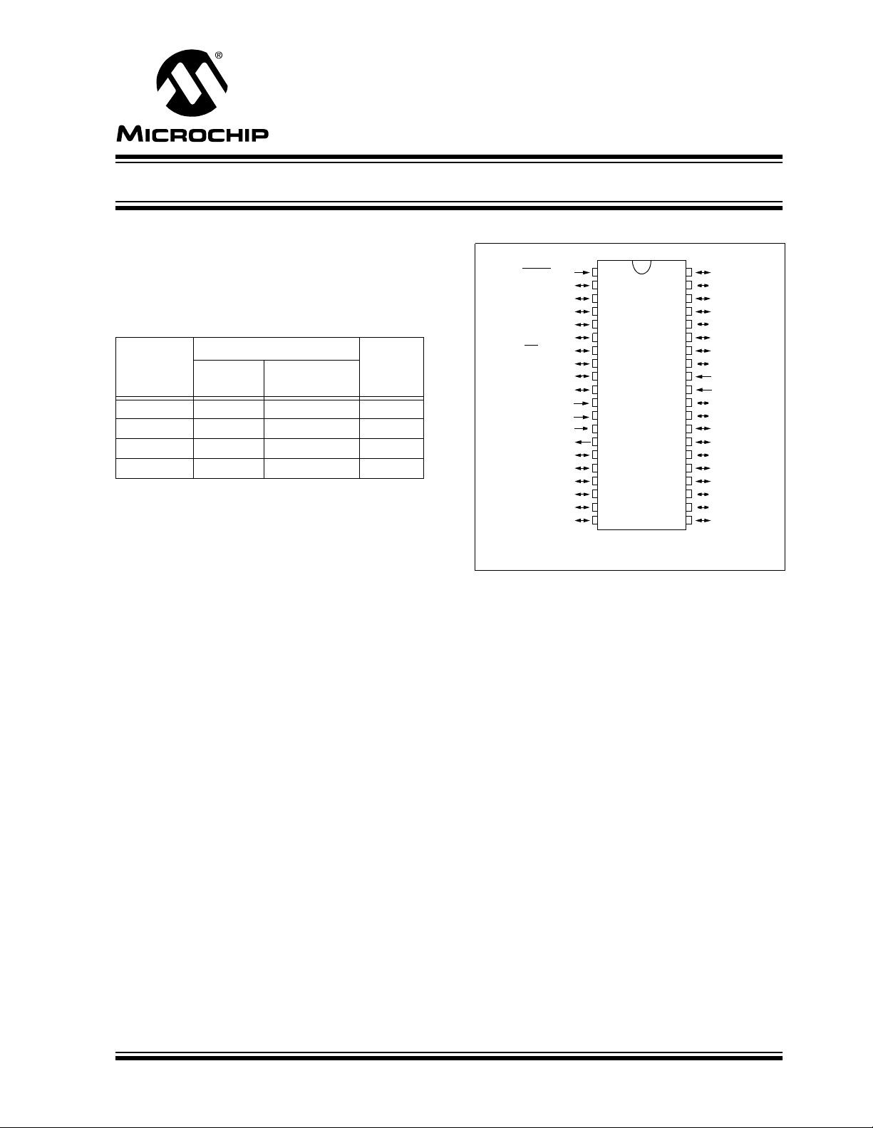
Pin Diagrams
DIP, Windowed CERDIP
RB7
RB6
RB5
RB4
RB3/CCP2
RB2/INT2
RB1/INT1
RB0/INT0
V
VSS
RD7/PSP7
RD6/PSP6
RD5/PSP5
RD4/PSP4
RC7/RX/DT
RC6/TX/CK
RC5/SDO
RC4/SDI/SDA
RD3/PSP3
RD2/PSP2
*
DD
DD
1
0
2
3
4
5
6
7
8
9
10
11
12
13
14
15
*
16
17
18
19
20
MCLR/VPP
RA0/AN
RA1/AN1
RA2/AN2/V
RA3/AN3/V
RA5/AN4/SS
OSC2/CLKO/RA6
RC0/T1OSO/T1CKI
RC1/T1OSI/CCP2
RC3/SCK/SCL
* RB3 is the alternate pin for the CCP2 pin multiplexing.
REF-
REF+
RA4/T0CKI
/LVDIN
RE0/RD/AN5
RE1/WR/AN6
RE2/CS/AN7
V
VSS
OSC1/CLKI
RC2/CCP1
RD0/PSP0
RD1/PSP1
40
39
38
37
36
35
34
33
32
31
30
29
PIC18C4X2
28
27
26
25
24
23
22
21
NOTE: Pin compatible with 40-pin PIC16C7X devices
Analog Features:
• 10-bit Analog-to-Digital Converter module (A/D)
with:
- Fast sampling rate
- Conversio n a vailable during sl eep
- DNL = ±1 LSb, INL = ±1 LSb
• Programmable Low-Voltage Detection (LVD)
module
- Supports interrupt on low voltage detection
• Programmable Brown-out Reset (BOR)
Special Microcontroller Features:
• Power-on Reset (POR), Power-up Timer (PWRT)
and Oscillator Start-up Timer (OST)
• Watchdog Timer (WDT) with its own on-chip RC
oscillator for reliable operation
• Programmable code-protection
• Pow er saving SLEEP mode
• Selectable oscillator options including:
- 4X Phase Lock Loop (of primary oscillator)
- Secondary Oscillator (32 kHz) clock input
• In-Circuit Serial Programming (ICSP™) via two pins
CMOS Technology:
• Low-power, high-speed EPROM technology
• Fully static design
• Wide operating voltage range (2.5V to 5.5V)
• Industrial and Extended temperature ranges
• Low-power consumption
7/99 Microchip Technology Inc.
Preliminary DS39026B-page 1
PIC18CXX2
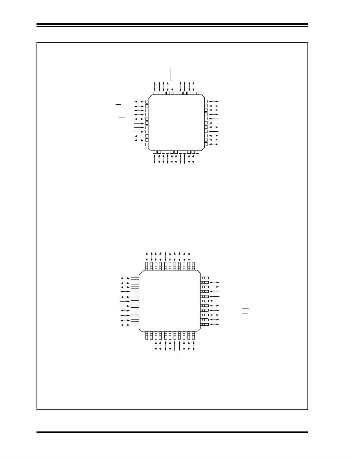
Pin Diagrams
PLCC
REF-
/VPP
RA4/T0CKI
RA5/AN4/SS
OSC2/CLKO/RA6
RC0/T1OSO/T1CKI
/LVDIN
/AN5
RE0/RD
RE1/WR/AN6
/AN7
RE2/CS
V
VSS
OSC1/CLKI
NC
RA3/AN3/VREF+
65432
7
8
9
10
11
DD
12
13
14
15
16
181920212223242526
17
RC2/CCP1
RC1/T1OSI/CCP2
NC
RB7
RA0/AN0
RB6
MCLR
1
44
43
RA2/AN2/V
RA1/AN1
PIC18C4X2
RC4/SDI/SDA
RD3/PSP3
RD2/PSP2
RD1/PSP1
RD0/PSP0
RC3/SCK/SCL
RB5
42
27
RC6/TX/CK
RC5/SDO
RB4
41
28
NC
NC
40
39
38
37
36
35
34
33
32
31
30
29
RB3/CCP2*
RB2/INT2
RB1/INT1
RB0/INT0
DD
V
VSS
RD7/PSP7
RD6/PSP6
RD5/PSP5
RD4/PSP4
RC7/RX/DT
*
RC6/TX/CK
RC5/SDO
RC4/SDI/SDA
RD3/PSP3
RD2/PSP2
RD1/PSP1
RD0/PSP0
RC3/SCK/SCL
RC2/CCP1
RC1/T1OSI/CCP2*NC
TQFP
4443424140
RC7/RX/DT
RD4/PSP4
RD5/PSP5
RD6/PSP6
RD7/PSP7
V
SS
VDD
RB0/INT0
RB1/INT1
RB2/INT2
RB3/CCP2
*
* RB3 is the alternate pin for the CCP2 pin multiplexing.
NOTE: Pin compatible with 44-pin PIC16C7X devices
1
2
3
4
5
6
7
8
9
10
11
121314
NC
NC
PIC18C4X2
15
RB5
RB4
16
RB6
39
17
RB7
38
363435
37
1819202122
RA2/AN2/V
RA1/AN1
RA0/AN0
MCLR
/VPP
REF-
33
32
31
30
29
28
27
26
25
24
23
RA3/AN3/VREF+
NC
RC0/T1OSO/T1CKI
OSC2/CLKO/RA6
OSC1/CLKI
SS
V
VDD
RE2/AN7/CS
RE1/AN6/WR
RE0/AN5/RD
RA5/AN4/SS/LVDIN
RA4/T0CKI
DS39026B-page 2 Preliminary
7/99 Microchip Technology Inc.
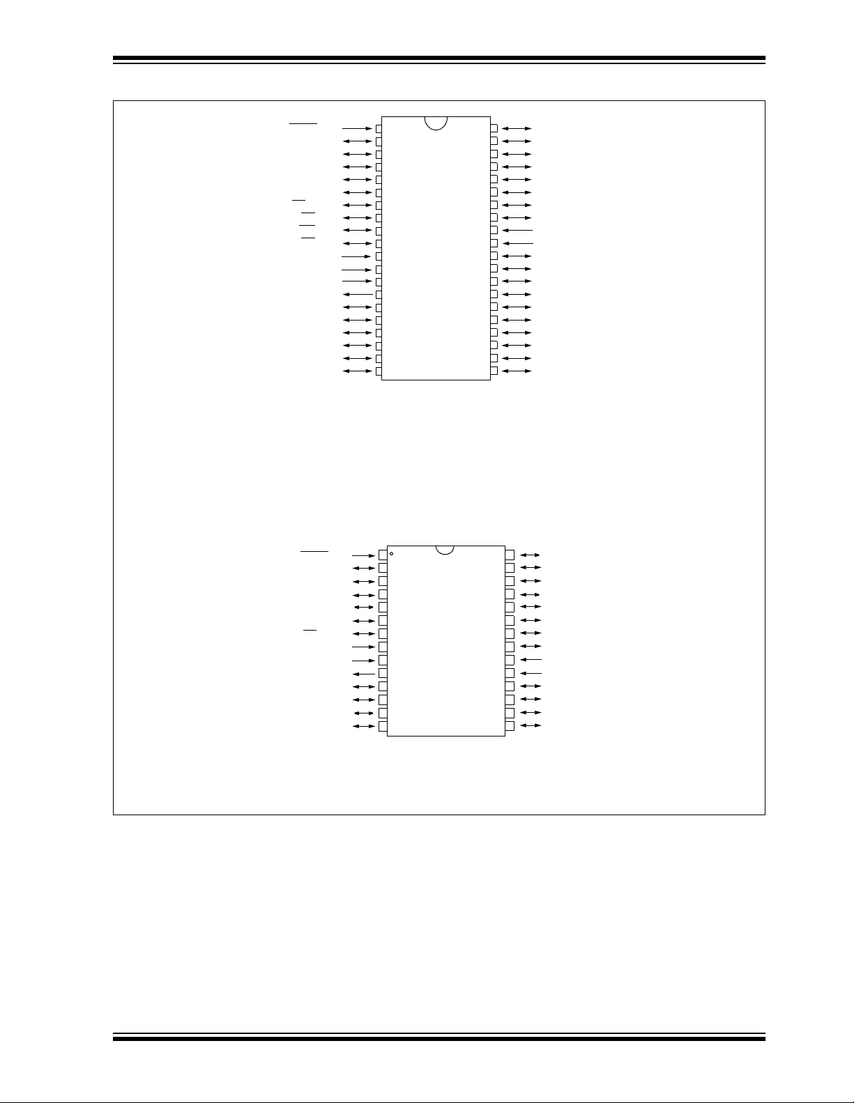
Pin Diagrams (Cont.’d)
PIC18CXX2
DIP, JW
MCLR/VPP
RA0/AN0
RA1/AN1
RA4/T0CKI
/LVDIN
RE0/RD
RE1/WR
RE2/CS
OSC1/CLKI
RC2/CCP1
RD0/PSP0
RD1/PSP1
REF-
REF+
/AN5
/AN6
/AN7
V
VSS
RA2/AN2/V
RA3/AN3/V
RA5/AN4/SS
OSC2/CLKO/RA6
RC0/T1OSO/T1CKI
RC1/T1OSI/CCP2
RC3/SCK/SCL
DD
1
2
3
4
5
6
7
8
9
10
11
12
13
14
*
15
16
17
18
19
20
NOTE: Pin compatible with 40-pin PIC16C7X devices
PIC18C4X2
40
39
38
37
36
35
34
33
32
31
30
29
28
27
26
25
24
23
22
21
RB7
RB6
RB5
RB4
RB3/CCP2
RB2/INT2
RB1/INT1
RB0/INT0
V
VSS
RD7/PSP7
RD6/PSP6
RD5/PSP5
RD4/PSP4
RC7/RX/DT
RC6/TX/CK
RC5/SDO
RC4/SDI/SDA
RD3/PSP3
RD2/PSP2
*
DD
DIP, SOIC, JW
MCLR/VPP
RA0/AN0
RA1/AN1
RA2/AN2/V
RA3/AN3/V
RA5/AN4/SS
OSC2/CLKO/RA6
RC0/T1OSO/T1CKI
RC1/T1OSI/CCP2
RC3/SCK/SCL
REF-
REF+
RA4/T0CKI
/LVDIN
V
OSC1/CLKI
RC2/CCP1
SS
*
* RB3 is the alternate pin for the CCP2 pin multiplexing.
NOTE: Pin compatible with 28-pin PIC16C7X devices
1
2
3
4
5
6
7
8
9
10
11
12
13
14
28
27
26
25
24
23
22
21
20
PIC18C2X2
19
18
17
16
15
RB7
RB6
RB5
RB4
RB3/CCP2
RB2/INT2
RB1/INT1
RB0/INT0
V
VSS
RC7/RX/DT
RC6/TX/CK
RC5/SDO
RC4/SDI/SDA
*
DD
7/99 Microchip Technology Inc.
Preliminary DS39026B-page 3

PIC18CXX2
Table of Contents
1.0 Device Overview..........................................................................................................................................................................5
2.0 Oscillator Configurations............................................................................................................................................................ 15
3.0 Reset..........................................................................................................................................................................................23
4.0 Memory Organization.................................................................................................................................................................33
5.0 Table Reads/Table Writes..........................................................................................................................................................53
6.0 8 X 8 Hardware Multiplier...........................................................................................................................................................61
7.0 Interrupts....................................................................................................................................................................................65
8.0 I/O Ports...................... ..................................... .......................... ....................................... ...................................... ................... 77
9.0 Timer0 Module ...........................................................................................................................................................................93
10.0 Timer1 Module ...........................................................................................................................................................................97
11.0 Timer2 Module .........................................................................................................................................................................102
12.0 Timer3 Module .........................................................................................................................................................................105
13.0 Capture/Compare/PWM (CCP) Modules .................................................................................................................................109
14.0 Master Synchronous Serial Port (MSSP) Module ....................................................................................................................117
15.0 Addressable Universal Synchronous Asynchronous Receiv er Transmitter (USA RT )..............................................................151
16.0 10-bit Analog-to-Digital Converter (A/D) Module......................................................................................................................167
17.0 Low Voltage Detect ..................................................................................................................................................................175
18.0 Special Features of the CPU.................................................................................................................................................... 181
19.0 Instruction Set Summary..........................................................................................................................................................191
20.0 Development Support. .............................................................................................................................................................. 235
21.0 Electrical Characteristics..........................................................................................................................................................241
22.0 DC and AC Characteristics Graphs and Tables.......................................................................................................................273
23.0 Packaging Information........................................... ............................................................................................................... .... 275
Appendix A: Revision History.........................................................................................................................................................283
Appendix B: Device Differences.....................................................................................................................................................283
Appendix C: Conversion Considerations.......................................................... .. ....... .... .. .... .. .. ....... ................................................284
Appendix D: Migration from Baseline to Enhanced Devices................................................... ....... .... .. .... .. ....................................284
Appendix E: Migration from Midrange to Enhanced Devices........................................................... .. .. .... .. .................................... 285
Appendix F: Migration from High-end to Enhanced Devices ......................................................................................................... 285
Index ....................................................................... .. .. ..... .... .. .. .. .. .. ....... .. .. .. .. .. .... .. ............................................................................287
On-Line Support...................................................................... .... .... .. ......... .... .. .... ....... .... ................................................................... 293
Reader Response..............................................................................................................................................................................294
PIC18CXX2 Product Identification System ........................................................................................................................................ 295
To Our Valued Customers
Most Current Data Sheet
To obtain the most up-to-date version of this data sheet, please register at our Worldwide Web site at:
http://www.microchip.com
You can determine the version of a data sheet by examining its literature number found on the bottom outside corner of any page.
The last character of the literature number is the version number. e.g., DS30000A is version A of document DS30000.
New Customer Notification System
Register on our web site (www.microchip.com/cn) to receive the most current information on our products.
Errata
An errata sheet may exist for current devices, describing minor operational differences (from the data sheet) and recommended
workarounds. As device/documentation issues become known to us, w e will pub lish an errata sheet. The errata will specify the re vision of silicon and revision of document to which it applies.
To determine if an errata sheet exists for a particular device, please check with one of the following:
• Microchip’s Worldwide Web site; http://www.microchip.com
• Your local Microchip sales office (see last page)
• The Microchip Corporate Literature Center; U.S. FAX: (602) 786-7277
When contacting a sales office or the literature center, please specify which device, revision of silicon and data sheet (include liter-
ature number) you are using.
Corrections to this Data Sheet
We constantly strive to improve the quality of all our products and documentation. We have spent a great deal of time to ensure
that this document is correct. However , w e realize that we ma y ha v e missed a f ew things . If y ou find any inf ormation that is missi n g
or appears in error, please:
• Fill out and mail in the reader response form in the back of this data sheet.
• E-mail us at webmaster@microchip.com.
We appreciate your assistance in making this a better document.
DS39026B-page 4 Preliminary
7/99 Microchip Technology Inc.

PIC18CXX2
1.0 DEVICE OVERVIEW
This document contains device-specific information for
the following four devices:
1. PIC18C242
2. PIC18C252
3. PIC18C442
4. PIC18C452
These devices come in 28 and 40-pin packages. The
28-pin devices do not have a Parallel Slave Port (PSP)
implemented and the numb er of Analog-to-Digital (A/D)
converter input channels is reduced to 5. An overview
of features is shown in Table 1-1.
The following two figures are device block diagrams
sorted by pin count; 28-pin f or Figur e 1-1 and 40-pin f or
Figure 1-2. The 28-pin and 40-pin pinouts are listed in
Table 1-2 and Table 1-3 respectively.
TABLE 1-1: DEVICE FEATURES
Features PIC18C242 PIC18C252 PIC18C442 PIC18C452
Operating Frequency DC - 40 MHz DC - 40 MHz DC - 40 MHz DC - 40 MHz
Program Memory (Bytes) 16K 32K 16K 32K
Program Memory (Instructions) 8192 16384 8192 16384
Data Memory (Bytes) 512 1536 512 1536
Interrupt sources 16 16 17 17
I/O Ports Ports A, B, C Ports A, B, C Ports A, B, C, D, E Ports A, B, C, D, E
Timers 4 4 4 4
Capture/Compare/PW M mod ul es 2 2 2 2
Serial Communications MSSP,
Addressable
USART
Parallel Communications — — PSP PSP
10-bit Analog-to-Digital Module 5 input channels 5 input channels 8 input channels 8 input channels
Resets (and Delays) POR, BOR,
Reset Instruction,
Stack Full,
Stack Underflow
(PWRT, OST)
Programmable Low Voltage Detect Yes Yes Yes Yes
Programmable Brown-out Reset Yes Yes Yes Yes
Instruction Set 75 Instructions 75 Instructions 75 Instructions 75 Instructions
Packages 28-pin DIP
28-pin SOIC
28-pin JW
MSSP,
Addressable
USART
POR, BOR,
Reset Instruction ,
Stack Full,
Stack Underflow
(PWRT, OST)
28-pin DIP
28-pin SOIC
28-pin JW
MSSP,
Addressable
USART
POR, BOR,
Reset Instruction,
Stack Full,
Stack Underflow
(PWRT, OST)
40-pin DIP
40-pin PLCC
40-pin TQFP
40-pin JW
MSSP,
Addressable
USART
POR, BOR,
Reset Instruction,
Stack Full,
Stack Underflow
(PWRT, OST)
40-pin DIP
40-pin PLCC
40-pin TQFP
40-pin JW
7/99 Microchip Technology Inc.
Preliminary DS39026B-page 5
PIC18CXX2
FIGURE 1-1: PIC18C2X2 BLOCK DIAGRAM
Data Bus<8>
Address Latch
Program Memory
(up to 2M Bytes)
OSC2/CLKO
OSC1/CLKI
T1OSI
T1OSO
21
Data Latch
16
21
Table Pointer < 2>
21
inc/dec logic
TABLELATCH
8
Instruction
Decode &
Control
Timing
Generation
4X PLL
Precision
Voltage
Reference
20
8
PCLATH
PCLATU
PCH
PCU
Program Counter
31 Level Stack
ROMLATCH
Instruction
Register
Power-up
Timer
Oscillator
Start-up Timer
Power-on
Reset
Watchdog
Timer
Brown-out
Reset
MCLR
8
VDD, VSS
PCL
8
4
BSR
Decode
BIT OP
3
8
Data Latch
Data RAM
Address Latch
12
Address<12>
12 4
FSR0
FSR1
FSR2
inc/dec
logic
PRODLPRODH
8 x 8 Multiply
WREG
8
8
ALU<8>
8
(2)
Bank0, F
PORTA
RA0/AN0
RA1/AN1
RA2/AN2/VREFRA3/AN3/VREF+
RA4/T0CKI
RA5/AN4/SS
RA6
/L VDIN
12
PORTB
RB0/INT0
RB1/INT1
RB2/INT2
8
RB3/CCP2
RB7:RB4
(1)
8
8
PORTC
RC0/T1OSO/T1CKI
RC1/T1OSI/CCP2
RC2/CCP1
RC3/SCK/SCL
RC4/SDI/SDA
RC5/SDO
RC6/TX/CK
RC7/RX/DT
(1)
Timer0 Timer1 Timer2
Master
CCP1
CCP2
Synchronous
Serial Port
Timer3
Addressable
USART
A/D Converter
Note1: Optional multiplexing of CCP2 input/output with RB3 is enabled by selection of configuration bit.
2: The high order bits of the Direct Address for the RAM are from the BSR register (except for the MOVFF
instruction).
3: Many of the general purpose I/O pins are multiplexed with one or more peripheral module functions. The
multiplexing combinations are device dependent.
DS39026B-page 6 Preliminary
7/99 Microchip Technology Inc.
FIGURE 1-2: PIC18C4X2 BLOCK DIAGRAM
Table Pointe r < 2 >
Address Latch
Program Memory
(up to 2M B y tes)
Data Latch
OSC2/CLKO
OSC1/CLKI
T1OSI
T1OSO
21
8
21
21
16
inc/dec logic
TABLELATCH
Instruction
Decode &
Control
Timing
Generation
4X PLL
20
8
PCLATU
PCLATH
PCH PCL
PCU
Program Counter
31 Level Stack
ROMLATCH
Instruction
Register
Power-up
Timer
Oscillator
Start-up Timer
Power-on
Reset
Watchdog
Timer
8
8
4
Decode
BIT OP
BSR
3
8
Data Bus<8>
Data Latch
Data RAM
(up to 4K
address reach )
Address Latch
12
Address<12>
12 4
Bank0, F
FSR0
FSR1
FSR2
inc/dec
logic
PRODLPRODH
8 x 8 Multiply
WREG
8
8
ALU<8>
PIC18CXX2
PORTA
(2)
PORTB
12
PORTC
8
8
8
PORTD
RA0/AN0
RA1/AN1
RA2/AN2/VREFRA3/AN3/VREF+
RA4/T0CKI
RA5/AN4/SS
RA6
RB0/INT0
RB1/INT1
RB2/INT2
RB3/CCP2
RB7:RB4
RC0/T1OSO/T1CKI
RC1/T1OSI/CCP2
RC2/CCP1
RC3/SCK/SCL
RC4/SDI/SDA
RC5/SDO
RC6/TX/CK
RC7/RX/DT
RD7/PSP7:RD0/PSP0
/L VDIN
(1)
(1)
Precision
Voltage
Reference
Timer0 Timer1 Timer2
CCP1
CCP2
Brown-out
MCLR
Reset
VDD, VSS
Master
Synchronous
Serial Port
8
Timer3
Addressable
USART
PORTE
RE0/AN5/RD
RE1/AN6/WR
RE2/AN7/CS
A/D Converter
Parallel Slave Port
Note1: Optional multiplexing of CCP2 input/output with RB3 is enabled by selection of configuration bit.
2: The high order bits of the Direc t Address f or the RAM are from the BSR registe r (e xce pt f or the M O VF F
instruction).
3: Many of the general purpose I/O pins are multiplexed with one or more peripheral module functions.
The multiplexing combinations are device dependent.
7/99 Microchip Technology Inc.
Preliminary DS39026B-page 7
PIC18CXX2
TABLE 1-2: PIC18C2X2 PINOUT I/O DESCRIPTIONS
Pin Name
MCLR
/VPP
MCLR
VPP
NC — — — — These pins should be left unconnected.
OSC1/CLKI
OSC1
CLKI
OSC2/CLKO/RA6
OSC2
CLKO
RA6
RA0/AN0
RA0
AN0
RA1/AN1
RA1
AN1
RA2/AN2/V
RA3/AN3/V
RA4/T0CKI
RA5/AN4/SS
RA6 See the OSC2/CLKO/RA6 pin.
Legend: TTL = TTL compatible input CMOS = CMOS compatible input or output
REF-
RA2
AN2
REF-
V
REF+
RA3
AN3
REF+
V
RA4
T0CKI
/LVDIN
RA5
AN4
SS
LVDIN
ST = Schmitt Trigger input with CMOS levels
I = Input O = Output
P = Power OD = Open Drain (no P diode to V
Pin Number
DIP SOIC Description
11
99
10 10
22
33
44
55
66
77
Pin
Type
Buffer
Type
I
P
I
I
O
O
I/O
I/O
I
I/O
I
I/O
I
I
I/O
I
I
I/OIST/OD
I/O
I
I
I
ST Master clear (reset) input. This pin is an active low reset
ST
CMOS
—
—
TTL
TTL
Analog
TTL
Analog
TTL
Analog
Analog
TTL
Analog
Analog
ST
TTL
Analog
ST
Analog
to the device.
Programming voltage input.
Oscillator crystal input or external clock source input.
ST buffer when configured in RC mode. CMOS otherwise.
External clock source input. Always associated with
pin function OSC1. (See related OSC1/CLKIN,
OSC2/CLKOUT pins).
Oscillator crystal output. Connects to crystal or
resonator in crystal oscillator mode.
In RC mode, OSC2 pin outputs CLKOUT which has 1/4
the frequency of OSC1, and denotes the instruction
cycle rate.
General Purpose I/O pin.
PORTA is a bi-directional I/O port.
Digital I/O.
Analog input 0.
Digital I/O.
Analog input 1.
Digital I/O.
Analog input 2.
A/D Reference Voltage (Low) input.
Digital I/O.
Analog input 3.
A/D Reference Voltage (High) input.
Digital I/O. Open drain when configured as output.
Timer0 external cloc k input .
Digital I/O.
Analog input 4.
SPI Slave Select input.
Low Voltage Detect Input.
DD)
DS39026B-page 8 Preliminary
7/99 Microchip Technology Inc.

TABLE 1-2: PIC18C2X2 PINOUT I/O DESCRIPTIONS (Cont.’d)
PIC18CXX2
Pin Name
RB0/INT0
RB0
INT0
RB1/INT1
RB1
INT1
RB2/INT2
RB2
INT2
RB3/CCP2
RB3
CCP2
RB4 25 25 I/O TTL Digital I/O.
RB5 26 26 I/O TTL Digital I/O.
RB6 27 27 I/O
RB7 28 28 I/O
Legend: TTL = TTL compatible input CMOS = CMOS compatible input or output
ST = Schmitt Trigger input with CMOS levels
I = Input O = Output
P = Power OD = Open Drain (no P diode to V
Pin Number
DIP SOIC Description
21 21
22 22
23 23
24 24
Pin
Type
I/O
I
I/O
I
I/O
I
I/O
I/O
I
I/O
Buffer
Type
PORTB is a bi-directional I/O port. PORTB can be software
programmed for internal weak pull-ups on all inputs.
TTLSTDigital I/O.
External Interrupt 0.
TTL
ST External Interrupt 1.
TTLSTDigital I/O.
External Interrupt 2.
TTLSTDigital I/O.
Capture2 input, Compare2 output, PWM2 output.
Interrupt on change pin.
Interrupt on change pin.
TTLSTDigital I/O.
Interrupt on change pin.
ICSP programming clock.
TTLSTDigital I/O.
Interrupt on change pin.
ICSP programming data.
DD)
7/99 Microchip Technology Inc.
Preliminary DS39026B-page 9

PIC18CXX2
TABLE 1-2: PIC18C2X2 PINOUT I/O DESCRIPTIONS (Cont.’d)
Pin Name
RC0/T1OSO/T1CKI
RC0
T1OSO
T1CKI
RC1/T1OSI/CCP2
RC1
T1OSI
CCP2
RC2/CCP1
RC2
CCP1
RC3/SCK/SCL
RC3
SCK
SCL
RC4/SDI/SDA
RC4
SDI
SDA
RC5/SDO
RC5
SDO
RC6/TX/CK
RC6
TX
CK
RC7/RX/DT
RC7
RX
DT
SS 8, 19 8, 19 P — Ground reference for logic and I/O pins.
V
VDD 20 20 P — Positive supply for logic and I/O pins.
Legend: TTL = TTL compatible input CMOS = CMOS compatible input or output
ST = Schmitt Trigger input with CMOS levels
I = Input O = Output
P = Power OD = Open Drain (no P diode to V
Pin Number
DIP SOIC Description
11 11
12 12
13 13
14 14
15 15
16 16
17 17
18 18
Pin
Type
I/O
O
I
I/O
I
I/O
I/O
I/O
I/O
I/O
I/O
I/O
I
I/O
I/O
O
I/O
O
I/O
I/O
I
I/O
Buffer
Type
ST
—
ST
ST
CMOS
ST
ST
ST
ST
ST
ST
ST
ST
ST
ST
—
ST
—
ST
ST
ST
ST
PORTC is a bi-directional I/O port.
Digital I/O.
Timer1 oscillator output.
Timer1/Timer3 external clock input.
Digital I/O.
Timer1 oscillator input.
Capture2 input, Compare2 output, PWM2 output.
Digital I/O.
Capture1 input/Compare1 output/PWM1 output.
Digital I/O.
Synchronous serial clock input/output for SPI mode.
Synchronous serial clock input/output for I
Digital I/O.
SPI Data In.
2
C Data I/O.
I
Digital I/O.
SPI Data Out.
Digital I/O.
USART Asynchronous Transmit.
USART Synchronous Clock.
(See related RX/DT)
Digital I/O.
USART Asynchronous Receive.
USART Synchronous Data.
(See related TX/CK)
DD)
2
C mode
DS39026B-page 10 Preliminary
7/99 Microchip Technology Inc.
TABLE 1-3: PIC18C4X2 PINOUT I/O DESCRIPTIONS
PIC18CXX2
Pin Name
MCLR
/VPP
MCLR
VPP
NC — — — These pins should be left unconnected.
OSC1/CLKI
OSC1
CLKI
OSC2/CLKO/RA6
OSC2
CLKO
RA6
RA0/AN0
RA0
AN0
RA1/AN1
RA1
AN1
RA2/AN2/V
RA3/AN3/V
RA4/T0CKI
RA5/AN4/SS
RA6 See the OSC2/CLKO/RA6 pin.
Legend: TTL = TTL compatible input CMOS = CMOS compatible input or output
REF-
RA2
AN2
REF-
V
REF+
RA3
AN3
REF+
V
RA4
T0CKI
/LVDIN
RA5
AN4
SS
LVDIN
ST = Schmitt Trigger input with CMOS levels
I = Input O = Output
P = Power OD = Open Drain (no P diode to V
Pin Number
DIP PLCC TQFP Description
1218
13 14 30
14 15 31
2319
3420
4521
5622
6723
7824
Pin
Type
I/O
I/O
I/O
I/O
I/O
I/OIST/OD
I/O
Buffer
Type
I
P
I
I
O
O
I
I
I
I
I
I
I
I
I
ST Master clear (reset) input. This pin is an active
ST
CMOS
—
—
TTL
TTL
Analog
TTL
Analog
TTL
Analog
Analog
TTL
Analog
Analog
ST
TTL
Analog
ST
Analog
low reset to the device.
Programming voltage input.
Oscillator crystal input or external clock
source input. ST buffer when configured in
RC mode. CMOS otherwise.
External clock source input. Always
associated with pin function OSC1. (See
related OSC1/CLKIN, OSC2/CLKOUT pins).
Oscillator crystal output. Connects to crystal
or resonator in crystal oscillator mode.
In RC mode, OSC2 pin outputs CLKOUT,
which has 1/4 the frequency of OSC1 and
denotes the instruction cycle rate.
General Purpose I/O pin.
PORTA is a bi-directional I/O port.
Digital I/O.
Analog input 0.
Digital I/O.
Analog input 1.
Digital I/O.
Analog input 2.
A/D Reference Voltage (Low) input.
Digital I/O.
Analog input 3.
A/D Reference Voltage (High) input.
Digital I/O . Open dr ain when config ured as outpu t.
Timer0 external clock input.
Digital I/O.
Analog input 4.
SPI Slave Select input.
Low Voltage Detect Input.
DD)
7/99 Microchip Technology Inc.
Preliminary DS39026B-page 11

PIC18CXX2
TABLE 1-3: PIC18C4X2 PINOUT I/O DESCRIPTIONS (Cont.’d)
Pin Name
RB0/INT0
RB0
INT0
RB1/INT1
RB1
INT1
RB2/INT2
RB2
INT2
RB3/CCP2
RB3
CCP2
RB4 37 41 14 I/O TTL Digital I/O.
RB5 38 42 15 I/O TTL Digital I/O.
RB6 39 43 16 I/O
RB7 40 44 17 I/O
Legend: TTL = TTL compatible input CMOS = CMOS compatible input or output
ST = Schmitt Trigger input with CMOS levels
I = Input O = Output
P = Power OD = Open Drain (no P diode to VDD)
Pin Number
DIP PLCC TQFP Description
33 36 8
34 37 9
35 38 10
36 39 11
Pin
Type
I/O
I
I/O
I
I/O
I
I/O
I/O
I
I/O
Buffer
Type
PORTB is a bi-directional I/O port. PORTB can be
software programmed for internal weak pull-ups on all
inputs.
TTLSTDigital I/O.
External Interrupt 0.
TTL
ST External Interrupt 1.
TTLSTDigital I/O.
External Interrupt 2.
TTLSTDigital I/O.
Capture2 input, Compare2 output, PWM2 output.
Interrupt on change pin.
Interrupt on change pin.
TTLSTDigital I/O.
Interrupt on change pin.
ICSP programming clock.
TTLSTDigital I/O.
Interrupt on change pin.
ICSP programming data.
DS39026B-page 12 Preliminary
7/99 Microchip Technology Inc.

TABLE 1-3: PIC18C4X2 PINOUT I/O DESCRIPTIONS (Cont.’d)
PIC18CXX2
Pin Name
RC0/T1OSO/T1CKI
RC0
T1OSO
T1CKI
RC1/T1OSI/CCP2
RC1
T1OSI
CCP2
RC2/CCP1
RC2
CCP1
RC3/SCK/SCL
RC3
SCK
SCL
RC4/SDI/SDA
RC4
SDI
SDA
RC5/SDO
RC5
SDO
RC6/TX/CK
RC6
TX
CK
RC7/RX/DT
RC7
RX
DT
Legend: TTL = TTL compatible input CMOS = CMOS compatible input or output
ST = Schmitt Trigger input with CMOS levels
I = Input O = Output
P = Power OD = Open Drain (no P diode to V
Pin Number
DIP PLCC TQFP Description
15 16 32
16 18 35
17 19 36
18 20 37
23 25 42
24 26 43
25 27 44
26 29 1
Pin
Type
I/O
O
I
I/O
I
I/O
I/O
I/O
I/O
I/O
I/O
I/O
I
I/O
I/O
O
I/O
O
I/O
I/O
I
I/O
Buffer
Type
ST
—
ST
ST
CMOS
ST
ST
ST
ST
ST
ST
ST
ST
ST
ST
—
ST
—
ST
ST
ST
ST
PORTC is a bi-directional I/O port.
Digital I/O.
Timer1 oscillator output.
Timer1/Timer3 external clock input.
Digital I/O.
Timer1 oscillator input.
Capture2 input, Compare2 output, PWM2 output.
Digital I/O.
Capture1 input/Compare1 output/PWM1 output.
Digital I/O.
Synchronous serial clock input/output for
SPI mode.
Synchronous serial clock input/output for
2
C mode.
I
Digital I/O.
SPI Data In.
2
C Data I/O.
I
Digital I/O.
SPI Data Out.
Digital I/O.
USART Asynchronous Transmit.
USART Synchronous Clock.
(See related RX/DT)
Digital I/O.
USART Asynchronous Re ceive.
USART Synchronous Data.
(See related TX/CK)
DD)
7/99 Microchip Technology Inc.
Preliminary DS39026B-page 13

PIC18CXX2
TABLE 1-3: PIC18C4X2 PINOUT I/O DESCRIPTIONS (Cont.’d)
Pin Name
RD0/PSP0 19 21 38 I/O ST
RD1/PSP1 20 22 39 I/O ST
RD2/PSP2 21 23 40 I/O ST
RD3/PSP3 22 24 41 I/O ST
RD4/PSP4 27 30 2 I/O ST
RD5/PSP5 28 31 3 I/O ST
RD6/PSP6 29 32 4 I/O ST
RD7/PSP7 30 33 5 I/O ST
RE0/RD
RE1/WR
RE2/CS
V
VDD 11, 32 12, 35 7, 28 P — Positive supply for logic and I/O pins.
Legend: TTL = TTL compatible input CMOS = CMOS compatible input or output
/AN5
RE0
RD
AN5
/AN6
RE1
WR
AN6
/AN7
RE2
CS
AN7
SS 12, 31 13, 34 6, 29 P — Ground reference for logic and I/O pins.
ST = Schmitt Trigger input with CMOS levels
I = Input O = Output
P = Power OD = Open Drain (no P diode to V
Pin Number
DIP PLCC TQFP Description
8 9 25 I/O
9 10 26 I/O
10 11 27 I/O
Pin
Type
Buffer
Type
TTL
TTL
TTL
TTL
TTL
TTL
TTL
TTL
ST
TTL
Analog
ST
TTL
Analog
ST
TTL
Analog
PORTD is a bi-directional I/O port.
Parallel Slave Po rt (PSP) for interfacing to a microprocessor port. These pins have TTL input buffers when
PSP module is enabled.
Digital I/O.
Parallel Slave Port Data.
Digital I/O.
Parallel Slave Port Data.
Digital I/O.
Parallel Slave Port Data.
Digital I/O.
Parallel Slave Port Data.
Digital I/O.
Parallel Slave Port Data.
Digital I/O.
Parallel Slave Port Data.
Digital I/O.
Parallel Slave Port Data.
Digital I/O.
Parallel Slave Port Data.
PORTE is a bi-directional I/O port.
Digital I/O.
Read control for parallel slave port.
(See also WR
Analog input 5.
Digital I/O.
Write control for parallel slave port.
(See CS
Analog input 6.
Digital I/O.
Chip Select control for parallel slave port.
(See related RD
Analog input 7.
and CS pins)
and RD pins)
and WR)
DD)
DS39026B-page 14 Preliminary
7/99 Microchip Technology Inc.

PIC18CXX2
2.0 OSCILLATOR CONFIGURATIONS
2.1 Oscillator Types
The PIC18CXX2 can be operated in eight different
oscillator modes. The user can program three configuration bits (FOSC 2, FOSC 1, an d FOSC0 ) to s elect one
of these eight modes:
1. LP Low Power Crystal
2. XT Crystal/Resonator
3. HS High Speed Crystal/Resonator
4. HS + PLL High Speed Crystal/Resonator with
PLL enabled
5. RC External Resistor/Capacitor
6. RCIO External Resistor/Capacitor with
I/O pin enabled
7. EC External Clock
8. ECIO External Clock with I/O pin enabled
2.2 Crystal Oscillator/Ceramic Resonators
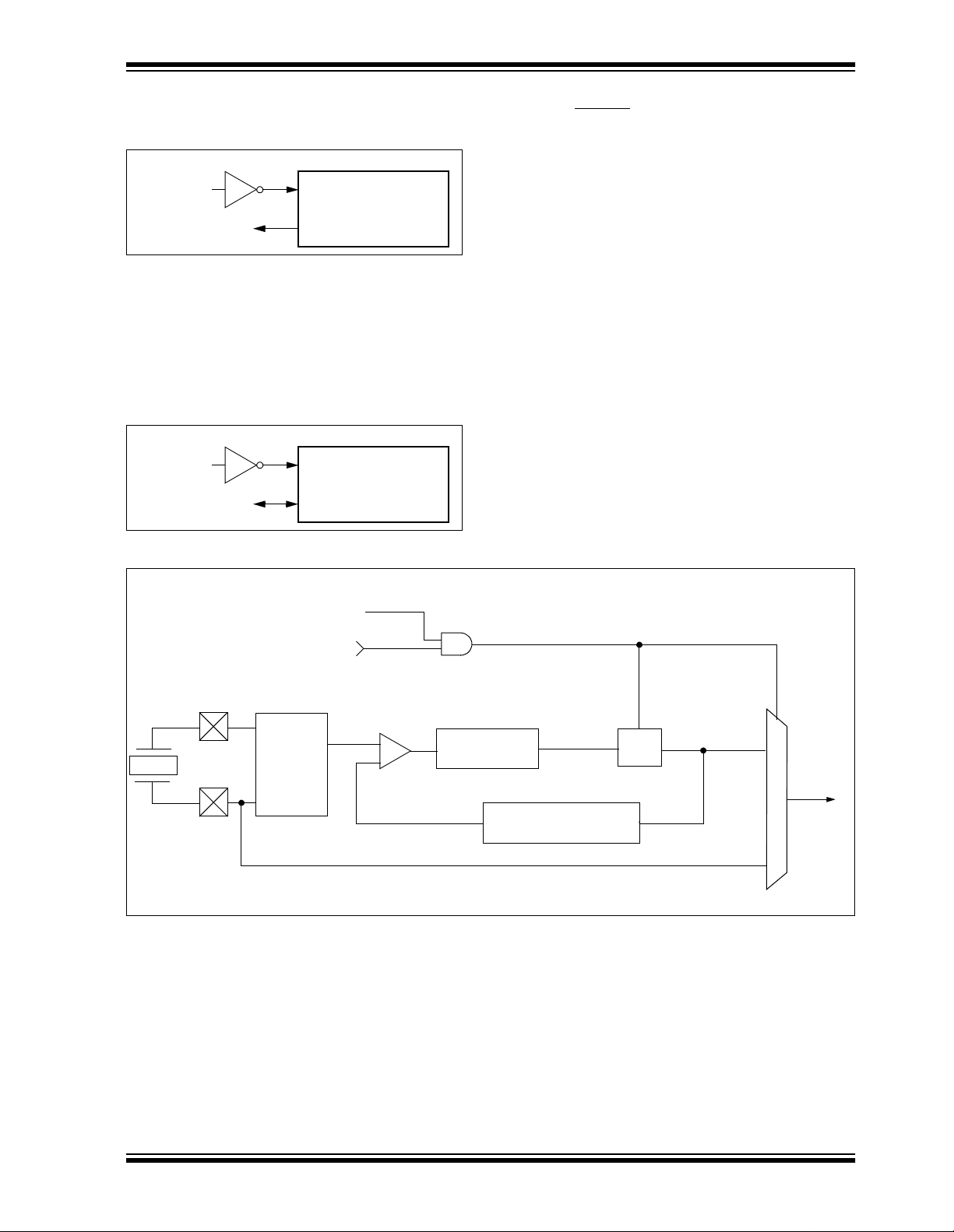
In XT, LP, HS or HS-PLL oscillator modes, a crystal or
ceramic resonator is connected to the OSC1 and
OSC2 pins to establish oscillation. Figure 2-1 shows
the pin connec tions. An ex ternal clock source ma y als o
be connected to the OSC1 pin in these modes, as
shown in Figure2-2.
The PIC18CXX2 oscillat or desi gn requ ires th e use o f a
parallel cut crystal.
Note: Use of a series cut crystal may give a fre-
quency out of the crystal manufacturers
specifications.
FIGURE 2-1: CRYSTAL/CERAMIC
RESONATOR OPERATION
(HS, XT OR LP
OSC CONFIGURATION)
(1)
C1
(1)
C2
Note 1: See Table 2-1 and Table 2-2 for recom-
Note 2: A series resistor (RS) may be required
Note 3: R
OSC1
XTAL
(2)
RS
OSC2
mended values of C1 and C2.
for AT strip cut crystals.
F varies with the crystal chosen.
RF
(3)
SLEEP
PIC18CXXX
To
internal
logic
FIGURE 2-2: EXTERNAL CLOCK INPUT
OPERATION (HS, XT OR LP
OSC CONFIGURATION)
Clock from
ext. system
Open
OSC1
PIC18CXXX
OSC2
7/99 Microchip Technology Inc.
Preliminary DS39026B-page 15
PIC18CXX2
TABLE 2-1: CERAMIC RESONATORS
Ranges Tested:
Mode Freq OSC1 OSC2
XT 455 kHz
2.0 MHz
4.0 MHz
HS 8.0 MHz
16.0 MHz
These values are for design guidance only. See
notes at bottom of page.
68 - 100 pF
15 - 68 pF
15 - 68 pF
10 - 68 pF
10 - 22 pF
68 - 100 pF
15 - 68 pF
15 - 68 pF
10 - 68 pF
10 - 22 pF
Resonators Used:
455 kHz Panasonic EFO-A455K04B
2.0 MHz Murata Erie CSA2.00MG
4.0 MHz Murata Erie CSA4.00MG
8.0 MHz Murata Erie CSA8.00MT
16.0 MHz Murata Erie CSA16.00MX
All resonators used did not have built-in capacitors.
0.3%
±
0.5%
±
0.5%
±
0.5%
±
0.5%
±
TABLE 2-2: CAPACITOR SELECTION FOR
CRYSTAL OSCILLATOR
Osc Type
LP 32.0 kHz 33 pF 33 pF
XT 200 kHz 47-68 pF 47-68 pF
HS 4.0 MHz 15 pF 15 pF
32.0 kHz Epson C-001R32.768K-A ± 20 PPM
200 kHz STD XTL 200.000KHz ± 20 PPM
1.0 MHz ECS ECS-10-13-1 ± 50 PPM
4.0 MHz ECS ECS-40-20-1 ± 50 PPM
8.0 MHz EPSON CA-301 8.000M-C ± 30 PPM
20.0 MHz E PS ON CA-301 20.000M-C ± 30 PPM
Crystal
Freq
200 kHz 15 pF 15 pF
1.0 MHz 15 pF 15 pF
4.0 MHz 15 pF 15 pF
8.0 MHz 15-33 pF 15-33 pF
20.0 MHz 15-33 pF 15-33 pF
25.0 MHz TBD TBD
These values are for design guidance only. See
notes at bottom of page.
Cap. Range
C1
Crystals Used
Cap.
Range
C2
Note1: Recommended values of C1 and C2 are
identical to the ranges tested (Table 2-1).
2: Higher capacitance increases the stability
of the oscillator, but also increases the st artup time.
3: Since each r esonator/crystal has its own
characteristics, the user should consult the
resonator/crystal manufacturer for app ropri ate values of external components.
4: Rs may be required in HS mode, as well as
XT mode, to avoid overdriving crystals with
low drive level specification.
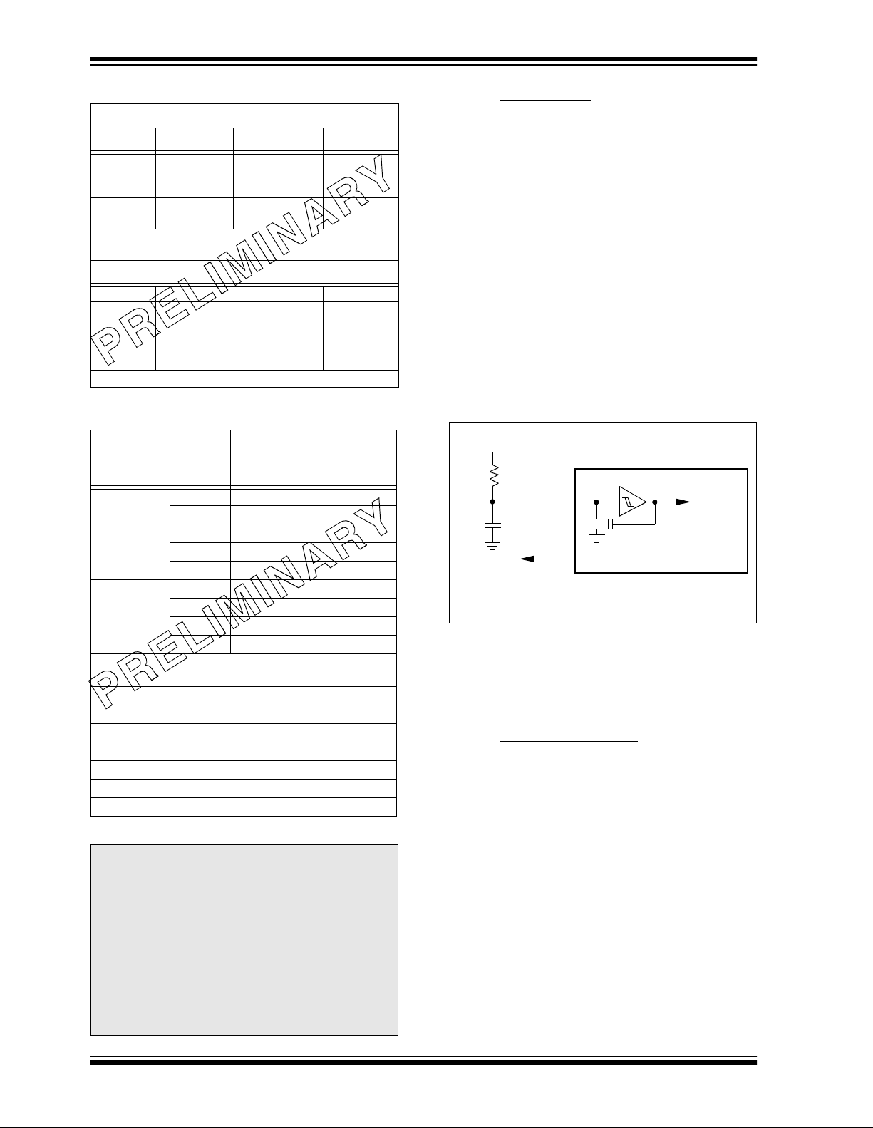
2.3 RC Oscillator
For timing insensitive applications, the “RC” and
"RCIO" device options offer additional cost savings.
The RC oscillator frequency is a function of the supply
voltage, the resistor (R
EXT) and capacitor ( CEXT) val-
ues and the operating temperature. In addition to this,
the oscillator frequency will vary from unit to unit due
to normal process parameter variation. Furthermore,
the difference in lead frame capacitance between
package types will also affect the oscillation frequency,
especially for low C
EXT values. The user also needs to
take into account variation due to tolerance of external
R and C components used. Figure 2-3 shows how the
R/C combination is connected.
In the RC oscillator mode, the oscillator frequency
divided by 4 is available on the OSC2 pin. This signal
may be used for test purposes or to synchronize other
logic.
FIGURE 2-3: RC OSCILLATOR MODE
VDD
REXT
OSC1
CEXT
VSS
F
Recommended values: 3 kΩ ≤ REXT ≤ 100 k
OSC/4
OSC2/CLKO
EXT > 20pF
C
Internal
clock
PIC18CXXX
Ω
The RCIO oscillator mode functions like the RC mode,
except that the OSC2 pin becomes an additional general purpose I/O pin. The I/O pin becomes bit 6 of
PORTA (RA6).
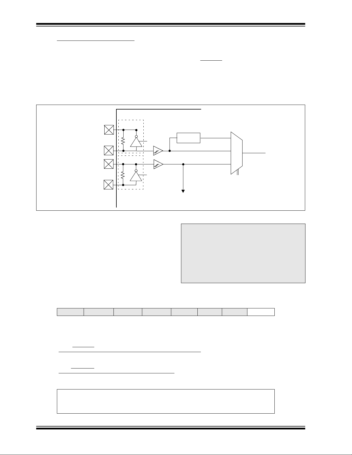
2.4 External Clock Input
The EC and ECIO oscillator mode s require an e xternal
clock source to be connected to the OSC1 pi n. The
feedback device between OSC1 and OSC2 is turned
off in these modes to sa v e current. There is no osc illator startup time required after a Power-On-Reset or
after a recovery from SLEEP mode.
In the EC oscillator mode, the oscillator frequency
divided by 4 is available on the OSC2 pin. This signal
may be used for test purposes or to synchronize other
logic. Figure 2-4 shows the pin conne cti ons for the EC
oscillator mode.
DS39026B-page 16 Preliminary
7/99 Microchip Technology Inc.
PIC18CXX2
FIGURE 2-4: E XTERN AL CLOCK INPUT
OPERATION
(EC OSC CONFIGURATION)
Clock from
ext. system
OSC/4
F
The ECIO oscillator mode functions like the EC mode,
except that the OSC 2 pin be comes a n addit ional general purpose I/O pin. The I/O pin becomes Bit 6 of
PORTA (RA6). Figure 2-5 shows the pin connections
for the ECIO oscillator mode.
OSC1
PIC18CXXX
OSC2
FIGURE 2-5: E XTERN AL CLOCK INPUT
OPERATION
(ECIO CONFIGURATION)
Clock from
ext. system
RA6
OSC1
PIC18CXXX
I/O (OSC2)
2.5 HS/PLL
A Phase Locked Loop circuit is provided as a programmable option for users that want to multiply the frequency of the incoming crystal oscillator signal by 4.
For an input clock frequency of 10 MHz, the internal
clock frequency will be multiplied to 40 MHz. This is
useful for customers who are concerned with EMI due
to high frequency crystals.
The PLL can only be enabled when the oscillator configuration bits are programmed for HS mode. If they
are programmed for any other mode, the PLL is not
enabled and the system clock will come directly from
OSC1.
The PLL is one of the modes of the FOSC<2:0> configuration bits. The oscillator mode is specified during
device programming.
A PLL lock timer is used to ensure that the PLL has
locked before device execution starts. The PLL lock
timer has a time-out that is called T
PLL.
FIGURE 2-6: PLL BLOCK DIAGRAM
(from configuration
HS Osc
bit register)
PLL Enable
OSC2
Phase
Comparator
IN
F
Crystal
Osc
FOUT
OSC1
Loop
Filter
Divide by 4
VCO
SYSCLK
MUX
7/99 Microchip Technology Inc.
Preliminary DS39026B-page 17
PIC18CXX2
2.6 Oscillator Switching Feature
The PIC18CXX2 devices include a feature that allows
the system clock source to be switched from the main
oscillator to an alternate low frequency clock source.
For the PIC18CXX2 devices, this alternate clock
source is the Timer1 oscilla tor . If a low-freque ncy crystal (32 KHz, for example) has been attached to the
Timer1 oscillator pins and the Timer1 oscillator has
FIGURE 2-7: DEVICE CLOCK SOURCES
PIC18CXXX
OSC2
OSC1
T1OSO
T1OSI
Main Oscillator
Sleep
Timer1 Oscillator
T1OSCEN
Enable
Oscillator
been enabled, the device can switch to a low power
execution mode. Figure2-7 shows a block diagram of
the system clock sources. The clock switching feature
is enabled by programming the Oscillator Switching
Enable (OSCSEN
) bit in Configuration R eg ist er1 H to a
’0’. Clock switching is disabled in an erased device.
See Section 9 f or further details of the T imer1 oscillator .
See Section 18.0 for Configuration Register details.
4 x PLL
TOSC
TT1P
Clock Source option
for other modules
Tosc/4
MUX
Clock
Source
TSCLK
2.6.1 SYSTEM CLOCK SWITCH BIT The system clock source switching is performed under
software control. The system clock switch bit, SCS
(OSCCON<0>) controls the cloc k s wi tching . Whe n the
SCS bit is ’0’, the system clock source comes from the
main oscillator that is sel ect ed by the FOSC configur ation bits in Configuration Register1H. When the SCS
bit is set, th e system clock sour ce will come from the
Timer1 oscillator. The SCS bit is cleared on all forms
of reset.
Register 2-1: OSCCON Register
U-0 U-0 U-0 U-0 U-0 U-0 U-0 R/W-1
— — — — — — —
bit 7 bit 0
bit 7-1 Unim plemented: Read as '0'
bit 0 SCS: System Clock Switch bit
OSCSEN configuration bit = ’0’ and T1OSCEN bit is set:
when
1 = Switch to Timer1 Oscillator/Clock pin
0 = Use primary Oscillator/Clock input pin
OSCSEN and T1OSCEN are in other states:
when
bit is forced clear
Note: The Timer1 oscillator must be enabled to
switch the system clock source. The
Timer1 osci llator i s enabled by setting t he
T1OSCEN bit in the Time r1 control register
(T1CON). If the Timer1 oscillator is not
enabled, then any write to the SCS bit will
be ignored (SCS bit forced cleared) and
the main oscillator will continue to be the
system clock source.
SCS
Legend
R = Readable bit W = Writable bit U = Unimplemented bit, read as ‘0’
- n = Value at POR reset ’1’ = Bit is set ’0’ = Bit is cleared x = Bit is unknown
DS39026B-page 18 Preliminary
7/99 Microchip Technology Inc.
PIC18CXX2
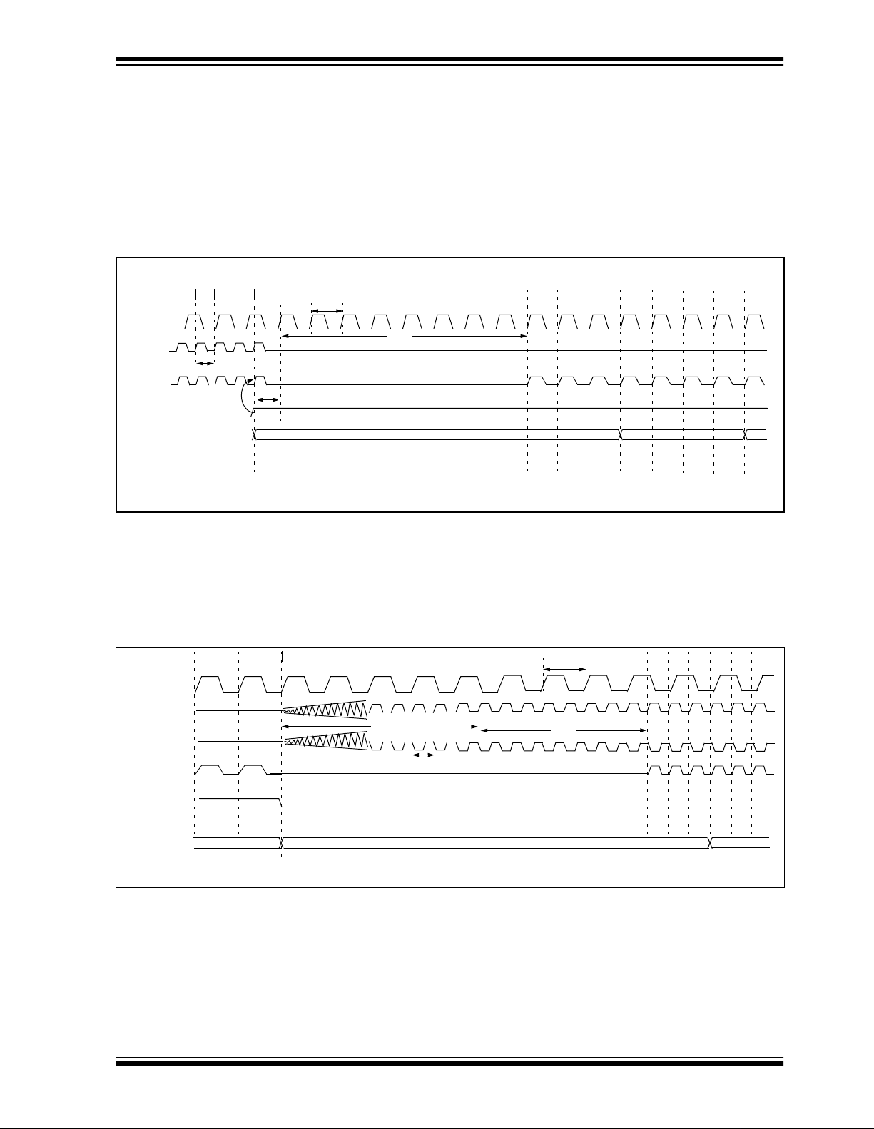
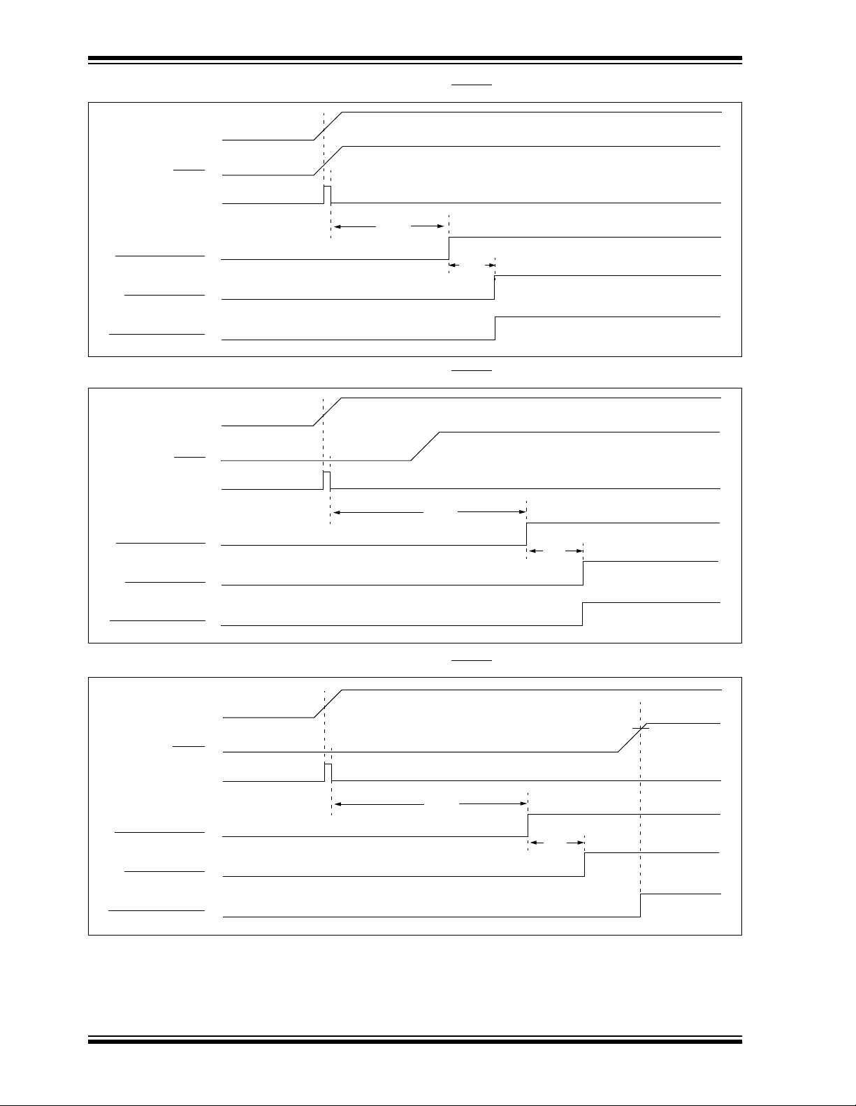
2.6.2 OSCILLATOR TRANSITIONS
A timing diagram indicating the transition from the
main oscillator to the Timer1 oscillator is shown in
The PIC18CXX2 devices contain circuitry to prevent
"glitches" when switching between oscillator sources.
Essential ly, the circuitry waits for eigh t ri sing ed ges of
the clock s ource t hat the pro cessor is s wi tching to . This
ensures that the new clock source is stable and that its
pulse width will not be less than the shortest pulse
Figure 2-8. The Timer1 oscillator is assumed to be
running all the time. After the SCS bit is set, the processor is frozen at the next occurring Q1 cycle. After
eight synchronization cycles are counted from the
Timer1 oscillator, operation resumes. No additional
delays are required after the synchronization cycles.
width of the two clock sources.
FIGURE 2-8: TIMING DIAGRAM FOR TRANSITION FROM OSC1 TO TIMER1 OSCILLATOR
Q1
T1OSI
OSC1
Internal
System
Clock
SCS
(OSCCON<0>)
Program
Counter
TOSC
Q1
TDLY
TT1P
21 345678
Tscs
PC + 2PC
Note1: Delay on internal system clock is eight oscillator cycles for synchronization.
Q3Q2Q1Q4Q3Q2
Q4 Q1
Q2 Q3 Q4 Q1
PC + 4
The sequence of events that takes place when switching from the Timer1 oscillator to the main oscillator will
depend on the mode of the main oscillator. In addition
to eight clock cycles of the main oscillator, additional
delays may take place.
If the main oscillator is configured for an external crystal (HS, XT, LP), then the transition will take place after
an oscillator startup time (T
OST) has occurred. A timing
diagram indicating the transition from the Timer1 oscillator to the main oscillator for HS, XT and LP modes is
shown in Figure 2-9.
FIGURE 2-9: TIMING FOR TRANSITION BETWEEN TIMER1 AND OSC1 (HS,XT,LP)
Q1 Q2 Q3 Q4 Q1 Q2
T1OSI
OSC1
OSC2
Internal System
Clock
SCS
(OSCCON<0>)
Program Counter
Q3 Q4
PC PC + 2
Q1
TOST
Note1: TOST = 1024TOSC (drawing not to scale).
TT1P
12345678
TSCS
TOSC
Q3
PC + 6
7/99 Microchip Technology Inc.
Preliminary DS39026B-page 19
PIC18CXX2
If the main oscillator is configured f or HS-PLL mode , an
oscillator startup time (T
timeout (T
PLL) will occur . The PL L timeout is typic ally 2
OST) plus an additional PLL
quency. A timing diagram indicating the tran sitio n from
the Timer1 oscillator to the main oscillator for HS-PLL
mode is shown in Figure 2 -10.
ms and allows the PLL to lock to the main o scillato r fre-
FIGURE 2-10: TIMING FOR TRANSITION BETWEEN TIMER1 AND OSC1 (HS WITH PLL)
Q4 Q1
T1OSI
OSC1
OSC2
PLL Clock
Input
Internal System
Program Counter
Clock
SCS
(OSCCON<0>)
TOST
PC PC + 2
TPLL
Note 1: TOST = 1024TOSC (drawing not to scale).
TT1P
TOSC
1 234 5678
TSCS
Q1 Q2 Q3 Q4 Q1 Q2
PC + 4
Q3
Q4
If the main os ci lla tor is c on fig ured in the RC, RCIO, EC
or ECIO modes, there is no oscillator startup timeout.
Operation will resume after eight cycles of the main
ing the transition from the Timer1 oscillator to the main
oscillator for R C, RCIO , EC and EC IO modes is shown
in Figure 2-11.
oscillator ha ve been count ed. A timing diagram indicat-
FIGURE 2-11: TIMING FOR TRANSITION BETWEEN TIMER1 AND OSC1 (RC, EC)
Q3 Q4
T1OSI
OSC1
OSC2
Internal System
Clock
SCS
(OSCCON<0>)
Program Counter
PC PC + 2
Note 1: RC oscillator mode assumed.
Q1
TOSC
1
TT1P
23
45678
TSCS
Q1 Q2 Q3 Q4 Q1 Q2 Q3
Q4
PC + 4
DS39026B-page 20 Preliminary
7/99 Microchip Technology Inc.
PIC18CXX2
2.7 Effects of Sleep Mode on the On-chip Oscillator
When the device e xec utes a SLEEP instruction, the onchip clocks and oscillator are turned off and the device
is held at the beginning of an instruction cycle (Q1
state). With the oscill ato r off, the OSC1 and OSC2 si gnals will stop oscillating. Since all the transistor switch-
ing currents have been rem o ved, sleep mode achiev e s
the lowest current consumption of the device (only
leakage currents). Enabling any on-chip feature that
will operate during sleep will increase the current consumed during sleep. The user can wake from SLEEP
through external reset, Watchdog Timer Reset or
through an interrupt.
TABLE 2-3: OSC1 AND OSC2 PIN STATES IN SLEEP MODE
OSC Mode OSC1 Pin OSC2 Pin
RC Floating, external resistor should pull
high
RCIO Floating, external resistor should pull
high
ECIO Floating Configured as Port A, bit 6
EC Floating At logic low
LP, XT, and HS Feedback inverter disabled, at quies-
cent voltage level
See Table 3-1, in the “Reset” section, for time-outs due to Sleep and MCLR
2.8 Power-up Delays
Pow er up dela ys are control led by two timers, so that n o
external reset circuitry is required f or most applic ations.
The delays ensure that the device is kept in RESET
until the device power supply and clock are stable. For
additional information on RESET operation, see the
“Reset” section.
The first timer is the Power-up Timer (PWRT), which
optionally provides a fixed delay of 72 ms (nominal) on
power-up only (POR and BOR). The second timer is
the Oscillator Start-up Timer OS T, intended to keep th e
chip in RESET until the crystal oscillator is stable.
With the PLL enabled (HS/PLL oscillator mode), the
time-out sequence following a power-on reset is different from other oscilla tor modes. Th e time-out seque nce
is as follows : First the PWR T time-o ut is inv ok ed after a
POR time delay has expired. Then the Oscillator Startup Timer (OST) is invoked. However, this is still not a
sufficient amount o f time to al low the PL L to loc k at high
frequencies. The PWRT timer is used to provide an
additional fix ed 2ms (nominal) ti me-out to a llow the PLL
ample time to lock to the incoming clock frequency.
At logic low
Configured as P o rt A, bit 6
Feedback inverter disabled, at quiescent voltage level
reset.
7/99 Microchip Technology Inc.
Preliminary DS39026B-page 21

PIC18CXX2
NOTES:
DS39026B-page 22 Preliminary
7/99 Microchip Technology Inc.
PIC18CXX2
3.0 RESET
The PIC18CXXX differentiates between various kinds
of reset:
a) Power-on Reset (POR)
b) MCLR
c) MCLR
d) Watchdog Timer (WDT) Reset (during normal
e) Programmable Brown-out Reset (BOR)
f) Reset Instruction
g) Stack Full rese t
h) Stack Underflow reset
Most registers are unaffected by a reset. Their status is
unknown on POR and unchanged by all other resets.
The other registers are forced to a “reset state” on
reset during normal operation
reset during SLEEP
operation)
Power-on Reset, MCLR
CLR reset during SLEEP and by the RESET instruc-
M
tion.
Most registers are not affected by a WDT wake-up,
since this is viewed as the resumption of normal operation. Stat us bit s from th e RCON r egiste r, RI
and BOR, are set or clea red diff er ently in diff ere nt
POR
reset situations, as indicated in Table 3-2. These bits
are used in software to determine the nature of the
reset. See Table 3-3 for a full descripti on of the rese t
states of all registers.
A simplified bl ock diag ram of the on-ch ip res et circui t is
shown in Figure 3-1.
The Enhanced MCU devices have a MCLR
in the MCLR
reset path. The filter wi ll detect a nd ignore
small pulses.
, WDT reset, Brown-out Reset,
A WDT reset does not drive MCLR pin low.
FIGURE 3-1: SIMPLIFIED BLOCK DIAGRAM OF ON-CHIP RESET CIRCUIT
RESET
Instruction
Stack
Pointer
Stack Full/Underflow Reset
External Reset
, TO, PD,
noise filter
MCLR
SLEEP
WDT
Time-out
Reset
Power-on Reset
BOREN
OST
10-bit Ripple counter
PWRT
10-bit Ripple counter
Enable PWRT
Enable OST
(2)
VDD
OSC1
Module
V
Brown-out
OST/PWRT
On-chip
RC OSC
WDT
DD rise
detect
Reset
(1)
Note1: This is a separate oscillator from the RC oscillator of the CLKIN pin.
2: See Table 3-1 for time-out situations.
S
Chip_Reset
R
Q
7/99 Microchip Technology Inc.
Preliminary DS39026B-page 23
PIC18CXX2
3.1 Power-On Reset (POR)
A Power-on Reset pulse is generated on-chip when
V
DD rise is detected. To take advantag e of the P OR cir-
cuitry , ju st tie the MC LR
tor) to V
DD. This will elimi nate e xternal R C compon ents
pin directly (or th rough a resi s-
usually needed to create a Power-on Reset delay. A
maximum rise time for VDD is specified (parameter
D004). For a slow rise time, see Figure 3-2.
When the device starts normal operation (exits the
reset condition), d evice operating p arameters (vol tage,
frequency , temperature ,...) must be m et to ensure operation. If these conditions are not met, the device must
be held in reset until the operating conditions are met.
Brown-out Reset may be used to meet the voltage
start-up condition.
FIGURE 3-2: EXTERN AL POWER-ON
RESET CIRCUIT (FOR SLOW
DD POWER-UP)
V
V
DD
D
R
R1
MCLR
C
Note1: External Po wer-on Reset cir cuit is required
only if the V
DD power-up s lop e i s too s low .
The diode D hel ps d isch arge th e ca pacito r
quickly when V
DD powers down.
2: R < 40 kΩ is recommended to make sure
that the voltage drop across R does not
violate the device’s electrical specification.
3: R1 = 100Ω to 1 kΩ will limit any current
flowing into MCLR
C in the event of MCLR/
down due to Electrostatic Discharge
(ESD) or Electrical Overstress (EOS).
PIC18CXXX
from external capacitor
VPP pin break-
3.2 Power-up Timer (PWRT)
The Power-up Timer provides a fixed nominal time-out
(parameter #33) only on power-up from the POR. The
Power-up Timer operates on an internal RC oscillator.
The chip is ke pt in reset a s lon g as the PW R T i s act iv e .
The PWRT’s time delay allows VDD to rise to an acceptable level. A configuration bit is provided to enable/disable the PWRT.
The power-up ti me dela y will v ary from chip-to-chi p due
DD, temperature and process variation. See DC
to V
parameter #33 for details.
3.3 Oscillator Start-up Timer (OST)
The Oscillator Start-up Timer (OST) provides 1024
oscillator cycle (from OSC1 input) delay after the
PWRT dela y is ov er (parameter #3 2). This ensures th at
the crystal oscillator or reso nator has started and stabilized.
The OST time-out is invoked only for XT, LP and HS
modes and only on Power-on Reset or wake-up from
SLEEP.
3.4 PLL Lock Timeout
With the PLL enabled, the timeout sequence following
a power-on reset is different from other oscillator
modes. A portion of the P ow er-up Timer is use d to provide a fixed timeout that is sufficient for the PLL to lock
to the main oscillator fre que nc y. This PLL lock timeout
PLL) is typically 2 ms and follows the oscillator startup
(T
timeout (OST).
3.5 Brown-Out Reset (BOR)
A configuration bit, BOREN, can disable (if clear/programmed) or enable (if set) the Brown-out Reset circuitry. If VDD falls below parameter D005 for greater
than parameter #35, the brown-out situation will reset
the chip. A reset may not occur if V
parameter D005 for less than parameter #35. The chip
will remain in Brown-out Reset until VDD rises above
DD. The Po wer-up Tim er will then be in vok ed and will
BV
keep the chip in RESET an additional time delay
(parameter #33). If VDD drops below BVDD while the
Power-up Timer is running, the chip will go back into a
Brown-out Reset and the Power-up Timer will be initialized. Once V
DD rises abo v e BV DD, the Power-up Timer
will execute the additional time delay.
DD falls below
DS39026B-page 24 Preliminary
7/99 Microchip Technology Inc.
PIC18CXX2
3.6 Time-out Sequence
On power-up , the time-out sequence is as f ollows: First,
PWRT time-out is invoked after the POR time delay has
expired. Then, OST is activated. The total time-out will
vary based on oscillat or config urati on and the s tatu s of
the PWRT. For example, in RC mode with the PWRT
disabled, there will be no time-out at all. Figure 3-3,
Figure 3-4, Figure 3-5, Figure 3-6 and Figure 3-7
depict time-out sequences on power-up.
Since the time-outs oc cur from the POR p ulse, if MC LR
is kept low long enough, the time-outs will expire.
Bringing MCLR
(Figure 3-5). This is useful for testing purposes or to
synchronize more than one PIC18CXXX device ope rating in parallel.
Table 3-2 shows the re set condi tio ns for som e Spe cial
Function Registers, while Table 3-3 shows the reset
conditions for all the registers.
high will begin execution immediately
TABLE 3-1: TIME-OUT IN VARIOUS SITUATIONS
Oscillator
Configuration
HS with PLL enabled
HS, XT, LP 72 ms + 1024Tosc 1024Tosc 72 ms + 1024Tosc 1024Tosc
EC 72 ms —72 ms —
External RC 72 ms — 72 ms —
Note1: 2 ms = Nominal time required for the 4x PLL to lock.
2: 72 ms is the nominal power-up timer delay
Power-up
(1)
72 ms + 1024Tosc + 2ms 1024Tosc + 2 ms 72 ms + 1024To sc + 2ms 1024Tosc + 2 ms
(2)
Brown-out
(2)
Wake-up from
SLEEP or
Oscillator SwitchPWRTE = 0 PWRTE = 1
Register 3-1: RCON Register Bits and Positions
R/W-0 R/W-0 U-0 R/W-1 R/W-1 R/W-1 R/W-1 R/W-1
IPEN LWRT
bit 7 bit 0
—RITO PD POR BOR
TABLE 3-2: STATUS BITS, THEIR SIGNIFICANCE AND THE INITIALIZATION CONDITION FOR
RCON REGISTER
Program
Condition
Power-on Reset 0000h 00-1 1100 1 1 1 0 0 u u
Reset during normal
MCLR
operation
Software Reset during normal
operation
Stack Full Reset during normal
operation
Stack Underflow Reset during
normal operation
MCLR Reset during SLEEP 0000h 00-u 10uu u 1 0 u u u u
WDT Reset 0000h 0u-u 01uu 1 0 1 u u u u
WDT Wake-up PC + 2 uu-u 00uu u 0 0 u u u u
Brown-out Reset 0000h 0u-1 11u0 1 1 1 1 0 u u
Interrupt wake-up from SLEEP
Legend: u = unchanged, x = unknown, — = unimplemented bit read as '0'.
Note1: When the wake-up is due to an interrupt and the GIEH or GIEL bits are set, the PC is loaded with the
interrupt vector (0x000008h or 0x000018h).
Counter
0000h 00-u uuuu u u u u u u u
0000h 0u-0 uuuu 0 u u u u u u
0000h 0u-u uu11 u u u u u u 1
0000h 0u-u uu11 u u u u u 1 u
PC + 2
RCON
Register RI TO PD POR BOR STKFUL STKUNF
(1)
uu-u 00uu u 1 0 u u u u
7/99 Microchip Technology Inc.
Preliminary DS39026B-page 25
PIC18CXX2
TABLE 3-3: INITIALIZATION CONDITIONS FOR ALL REGISTERS
MCLR
Resets
WDT Reset
Power-on Reset,
Register Applicable Devices
Brown-out Reset
TOSU 242 442 252 452 ---0 0000 ---0 0000
TOSH 242 442 252 452 0000 0000 0000 0000
TOSL 242 442 252 452 0000 0000 0000 0000
STKPTR 242 442 252 452 00-0 0000 00-0 0000
PCLATU 242 442 252 452 ---0 0000 ---0 0000 ---u uuuu
PCLATH 242 442 252 452 0000 0000 0000 0000 uuuu uuuu
PCL 242 442 252 452 0000 0000 0000 0000
TBLPTRU 242 442 252 452 --00 0000 --00 0000 --uu uuuu
TBLPTRH 242 442 252 452 0000 0000 0000 0000 uuuu uuuu
TBLPTRL 242 442 252 452 0000 0000 0000 0000 uuuu uuuu
TABLAT 242 442 252 452 0000 0000 0000 0000 uuuu uuuu
PRODH 242 442 252 452 xxxx xxxx uuuu uuuu uuuu uuuu
PRODL 242 442 252 452 xxxx xxxx uuuu uuuu uuuu uuuu
INTCON 242 442 252 452 0000 000x 0000 000u
INTCON2 242 442 252 452 1111 -1-1 1111 -1-1
INTCON3 242 442 252 452 11-0 0-00 11-0 0-00
INDF0 242 442 252 452 N/A N/A N/A
POSTINC0 242 442 252 452 N/A N/A N/A
POSTDEC0 242 442 252 452 N/A N/A N/A
PREINC0 242 442 252 452 N/A N/A N/A
PLUSW0 242 442 252 452 N/A N/A N/A
FSR0H 242 442 252 452 ---- 0000 ---- 0000 ---- uuuu
FSR0L 242 442 252 452 xxxx xxxx uuuu uuuu uuuu uuuu
WREG 242 442 252 452 xxxx xxxx uuuu uuuu uuuu uuuu
INDF1 242 442 252 452 N/A N/A N/A
POSTINC1 242 442 252 452 N/A N/A N/A
POSTDEC1 242 442 252 452 N/A N/A N/A
PREINC1 242 442 252 452 N/A N/A N/A
PLUSW1 242 442 252 452 N/A N/A N/A
Legend: u = unchanged, x = unknown, - = unimplemented bit, read as ’0’, q = value depends on condition
Note1: One or more bits in the INTCONx or PIRx registers will be affected (to cause wake-up).
2: When the wake-up is due to an interrupt and the GIEL or GIEH bit is set, the PC is loaded with the interrupt
vector (0008h or 0018h).
3: When the wake-up is due to an interrupt and the GIEL or GIEH bit is set, the TOSU, TO SH and TOSL are
updated with the current value of the PC. The STKPTR is modified to point to the next location in the hardware stack.
4: See Table 3-2 for reset value for specific condition.
5: Bit 6 of PORTA, LATA, and TRISA are enabled in ECIO and RCIO oscillator modes only. In all other
oscillator modes, they are disabled and read ’0’.
6: The long write enable is only reset on a POR or MCLR
7: Bit 6 of PORTA, LATA and TRISA are not available on all devices. When unimplemented, they are read ’0’.
Reset Instruction
Stack Resets
reset.
Wake-up via WDT
or Interrupt
---0 uuuu
uuuu uuuu
uuuu uuuu
uu-u uuuu
PC + 2
uuuu uuuu
uuuu -u-u
uu-u u-uu
(3)
(3)
(3)
(3)
(2)
(1)
(1)
(1)
DS39026B-page 26 Preliminary
7/99 Microchip Technology Inc.
PIC18CXX2
TABLE 3-3: INITIALIZATION CONDITIONS FOR ALL REGISTERS (Cont.’d)
MCLR
Resets
WDT Reset
Power-on Reset,
Register Applicable Devices
FSR1H 242 442 252 452 ---- 0000 ---- 0000 ---- uuuu
FSR1L 242 442 252 452 xxxx xxxx uuuu uuuu uuuu uuuu
BSR 242 442 252 452 ---- 0000 ---- 0000 ---- uuuu
INDF2 242 442 252 452 N/A N/A N/A
POSTINC2 242 442 252 452 N/A N/A N/A
POSTDEC2 242 442 252 452 N/A N/A N/A
PREINC2 242 442 252 452 N/A N/A N/A
PLUSW2 242 442 252 452 N/A N/A N/A
FSR2H 242 442 252 452 ---- 0000 ---- 0000 ---- uuuu
FSR2L 242 442 252 452 xxxx xxxx uuuu uuuu uuuu uuuu
STATUS 242 442 252 452 ---x xxxx ---u uuuu ---u uuuu
TMR0H 242 442 252 452 xxxx xxxx uuuu uuuu uuuu uuuu
TMR0L 242 442 252 452 xxxx xxxx uuuu uuuu uuuu uuuu
T0CON 242 442 252 452 1111 1111 1111 1111 uuuu uuuu
OSCCON 242 442 252 452 ---- ---0 ---- ---0 ---- ---u
LVDCON 242 442 252 452 --00 0101 --00 0101 --uu uuuu
WDTCON 242 442 252 452 ---- ---0 ---- ---0 ---- ---u
(4, 6)
RCON
TMR1H 242 442 252 452 xxxx xxxx uuuu uuuu uuuu uuuu
TMR1L 242 442 252 452 xxxx xxxx uuuu uuuu uuuu uuuu
T1CON 242 442 252 452 0-00 0000 u-uu uuuu u-uu uuuu
TMR2 242 442 252 452 xxxx xxxx uuuu uuuu uuuu uuuu
PR2 242 442 252 452 1111 1111 1111 1111 1111 1111
T2CON 242 442 252 452 -000 0000 -000 0000 -uuu uuuu
SSPBUF 242 442 252 452 xxxx xxxx uuuu uuuu uuuu uuuu
SSPADD 242 442 252 452 0000 0000 0000 0000 uuuu uuuu
SSPSTAT 242 442 252 452 0000 0000 0000 0000 uuuu uuuu
SSPCON1 242 442 252 452 0000 0000 0000 0000 uuuu uuuu
SSPCON2 242 442 252 452 0000 0000 0000 0000 uuuu uuuu
Legend: u = unchanged, x = unknown, - = unimplemented bit, read as ’0’, q = value depends on condition
Note1: One or more bits in the INTCONx or PIRx registers will be affected (to cause wake-up).
2: When the wake-up is due to an interrupt and the GIEL or GIEH bit is set, the PC is loaded with the interrupt
3: When the wake-up is due to an interrupt and the GIEL or GIEH bit is set, the TOSU, TO SH and TOSL are
4: See Table 3-2 for reset value for specific condition.
5: Bit 6 of PORTA, LATA, and TRISA are enabled in ECIO and RCIO oscillator modes only. In all other
6: The long write enable is only reset on a POR or MCLR
7: Bit 6 of PORTA, LATA and TRISA are not available on all devices. When unimplemented, they are read ’0’.
242 442 252 452 00-1 11q0 00-1 qquu uu-u qquu
vector (0008h or 0018h).
updated with the current value of the PC. The STKPTR is modified to point to the next location in the hard-
ware stack.
oscillator modes, they are disabled and read ’0’.
Brown-out Reset
Reset Instruction
Stack Resets
reset.
Wake-up via WDT
or Interrupt
7/99 Microchip Technology Inc.
Preliminary DS39026B-page 27

PIC18CXX2
TABLE 3-3: INITIALIZATION CONDITIONS FOR ALL REGISTERS (Cont.’d)
MCLR
Resets
WDT Reset
Power-on Reset,
Register Applicable Devices
ADRESH 242 442 252 452 xxxx xxxx uuuu uuuu uuuu uuuu
ADRESL 242 442 252 452 xxxx xxxx uuuu uuuu uuuu uuuu
ADCON0 242 442 252 452 0000 0000 0000 0000 uuuu uuuu
ADCON1 242 442 252 452 --0- 0000 --0- 0000 --u- uuuu
CCPR1H 242 442 252 452 xxxx xxxx uuuu uuuu uuuu uuuu
CCPR1L 242 442 252 452 xxxx xxxx uuuu uuuu uuuu uuuu
CCP1CON 242 442 252 452 --00 0000 --00 0000 --uu uuuu
CCPR2H 242 442 252 452 xxxx xxxx uuuu uuuu uuuu uuuu
CCPR2L 242 442 252 452 xxxx xxxx uuuu uuuu uuuu uuuu
CCP2CON 242 442 252 452 --00 0000 --00 0000 --uu uuuu
TMR3H 242 442 252 452 xxxx xxxx uuuu uuuu uuuu uuuu
TMR3L 242 442 252 452 xxxx xxxx uuuu uuuu uuuu uuuu
T3CON 242 442 252 452 0000 0000 uuuu uuuu uuuu uuuu
SPBRG 242 442 252 452 xxxx xxxx uuuu uuuu uuuu uuuu
RCREG 242 442 252 452 xxxx xxxx uuuu uuuu uuuu uuuu
TXREG 242 442 252 452 xxxx xxxx uuuu uuuu uuuu uuuu
TXSTA 242 442 252 452 0000 -01x 0000 -01u uuuu -uuu
RCSTA 242 442 252 452 0000 000x 0000 000u uuuu uuuu
IPR2 242 442 252 452 ---- 1111 ---- 1111 ---- uuuu
PIR2 242 442 252 452 ---- 0000 ---- 0000
PIE2 242 442 252 452 ---- 0000 ---- 0000 ---- uuuu
IPR1 242 442 252 452 1111 1111 1111 1111 uuuu uuuu
242 442 252 452 -111 1111 -111 1111 -uuu uuuu
PIR1
PIE1 242 442 252 452 0000 0000 0000 0000 uuuu uuuu
Legend: u = unchanged, x = unknown, - = unimplemented bit, read as ’0’, q = value depends on condition
Note1: One or more bits in the INTCONx or PIRx registers will be affected (to cause wake-up).
2: When the wake-up is due to an interrupt and the GIEL or GIEH bit is set, the PC is loaded with the interrupt
3: When the wake-up is due to an interrupt and the GIEL or GIEH bit is set, the TOSU, TO SH and TOSL are
4: See Table 3-2 for reset value for specific condition.
5: Bit 6 of PORTA, LATA, and TRISA are enabled in ECIO and RCIO oscillator modes only. In all other
6: The long write enable is only reset on a POR or MCLR
7: Bit 6 of PORTA, LATA and TRISA are not available on all devices. When unimplemented, they are read ’0’.
242 442 252 452 0000 0000 0000 0000
242 442 252 452 -000 0000 -000 0000
242
442 252 452 -000 0000 -000 0000 -uuu uuuu
vector (0008h or 0018h).
updated with the current value of the PC. The STKPTR is modified to point to the next location in the hard-
ware stack.
oscillator modes, they are disabled and read ’0’.
Brown-out Reset
Reset Instruction
Stack Resets
reset.
Wake-up via WDT
or Interrupt
---- uuuu
uuuu uuuu
-uuu uuuu
(1)
(1)
(1)
DS39026B-page 28 Preliminary
7/99 Microchip Technology Inc.
PIC18CXX2
TABLE 3-3: INITIALIZATION CONDITIONS FOR ALL REGISTERS (Cont.’d)
MCLR
Resets
WDT Reset
Power-on Reset,
Register Applicable Devices
Brown-out Reset
TRISE 242 442 252 452 0000 -111 0000 -111 uuuu -uuu
TRISD
242 442 252 452 1111 1111 1111 1111 uuuu uuuu
TRISC 242 442 252 452 1111 1111 1111 1111 uuuu uuuu
TRISB 242 442 252 452 1111 1111 1111 1111 uuuu uuuu
TRISA
(5, 7)
242 442 252 452
-111 1111
(5)
LATE 242 442 252 452 ---- -xxx ---- -uuu ---- -uuu
LATD 242 442 252 452 xxxx xxxx uuuu uuuu uuuu uuuu
LATC 242 442 252 452 xxxx xxxx uuuu uuuu uuuu uuuu
LATB 242 442 252 452 xxxx xxxx uuuu uuuu uuuu uuuu
LATA
(5, 7)
242 442 252 452
-xxx xxxx
(5)
PORTE 242 442 252 452 ---- -000 ---- -000 ---- -uuu
PORTD 242 442 252 452 xxxx xxxx uuuu uuuu uuuu uuuu
PORTC 242 442 252 452 xxxx xxxx uuuu uuuu uuuu uuuu
PORTB 242 442 252 452 xxxx xxxx uuuu uuuu uuuu uuuu
PORTA
(5, 7)
242 442 252 452
-x0x 0000
(5)
Legend: u = unchanged, x = unknown, - = unimplemented bit, read as ’0’, q = value depends on condition
Note1: One or more bits in the INTCONx or PIRx registers will be affected (to cause wake-up).
2: When the wake-up is due to an interrupt and the GIEL or GIEH bit is set, the PC is loaded with the interrupt
vector (0008h or 0018h).
3: When the wake-up is due to an interrupt and the GIEL or GIEH bit is set, the TOSU, TO SH and TOSL are
updated with the current value of the PC. The STKPTR is modified to point to the next location in the hardware stack.
4: See Table 3-2 for reset value for specific condition.
5: Bit 6 of PORTA, LATA, and TRISA are enabled in ECIO and RCIO oscillator modes only. In all other
oscillator modes, they are disabled and read ’0’.
6: The long write enable is only reset on a POR or MCLR
7: Bit 6 of PORTA, LATA and TRISA are not available on all devices. When unimplemented, they are read ’0’.
Reset Instruction
Stack Resets
-111 1111
-uuu uuuu
-u0u 0000
reset.
(5)
(5)
(5)
Wake-up via WDT
or Interrupt
-uuu uuuu
-uuu uuuu
-uuu uuuu
(5)
(5)
(5)
7/99 Microchip Technology Inc.
Preliminary DS39026B-page 29
PIC18CXX2
FIGURE 3-3: TIME-OUT SEQUENCE ON POWER-UP (MCLR TIED TO VDD)
VDD
MCLR
INTERNAL POR
TPWRT
PWRT TIME-OUT
OST TIME-OUT
INTERNAL RESET
TOST
FIGURE 3-4: TIME-OUT SEQUENCE ON POWER-UP (MCLR
VDD
MCLR
INTERNAL POR
TPWRT
PWRT TIME-OUT
OST TIME-OUT
INTERNAL RESET
NOT TIED TO VDD ): CASE 1
TOST
FIGURE 3-5: TIME-OUT SEQUENCE ON POWER-UP (MCLR
VDD
MCLR
INTERNAL POR
TPWRT
PWRT TIME-OUT
OST TIME-OUT
INTERNAL RESET
DS39026B-page 30 Preliminary
NOT TIED TO VDD ): CASE 2
TOST
7/99 Microchip Technology Inc.
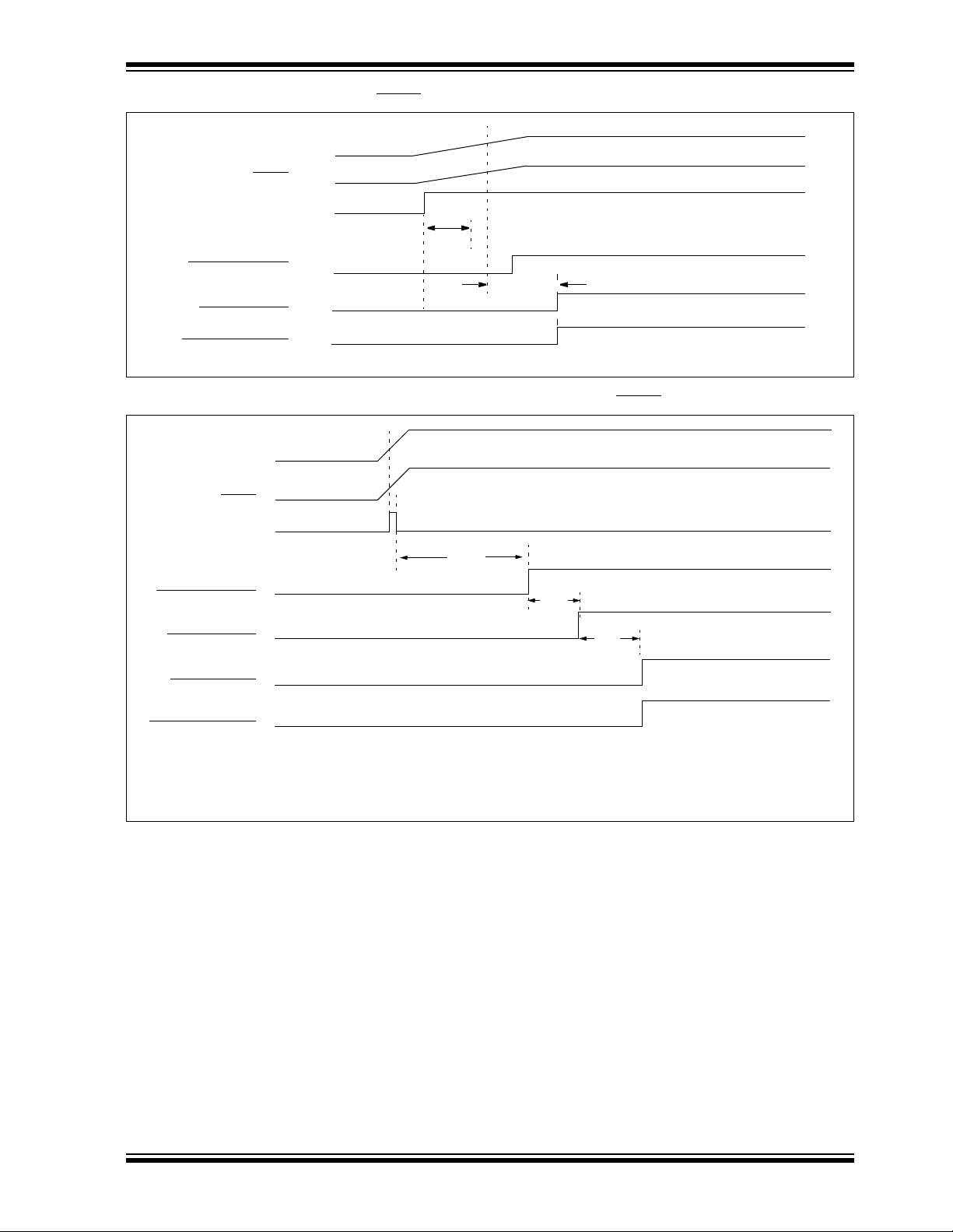
FIGURE 3-6: SLOW RISE TIME (MCLR TIED TO VDD)
VDD
MCLR
INTERNAL POR
0V
PWRT
T
1V
PIC18CXX2
5V
PWRT TIME-OUT
OST TIME-OUT
INTERNAL RES ET
TOST
FIGURE 3-7: TIME-OUT SEQUENCE ON POR W/ PLL ENABLED (MCLR
VDD
MCLR
IINTERNAL POR
TPWRT
PWRT TIME-OUT
OST TIME-OUT
PLL TIME-OUT
TOST
TPLL
TIED TO VDD)
INTERNAL RESET
TOST = 1024 clock cycles.
PLL ≈ 2 ms max. First three stages of the PWRT timer.
T
7/99 Microchip Technology Inc.
Preliminary DS39026B-page 31

PIC18CXX2
NOTES:
DS39026B-page 32 Preliminary
7/99 Microchip Technology Inc.

4.0 MEMORY ORGANIZATION
There are two memory blocks in Enhanced MCU
devices. These memory blocks are:
• Program Memory
• Data Memory
Each block has its own bus so that concurrent access
can occur .
4.1 Program Memory Organization
A 21-bit program counter is capable of addressing the
2-Mbyte program memory space. Ac ce ss in g a location
between the physically implemented memory and the
2-Mbyte address will cause a read of all ’0’s (a NOP
instructi on).
PIC18C252 and PIC18C452 have 32-KBytes of
EPROM, while PIC18C242 and PIC18C442 have
16-KBytes of EPROM. This means that PIC18CX52
devices can store up to 16K of sin gle word instructions, and PIC18CX42 devices can store up to 8K of
single word inst r u ct ions.
The reset vector address is at 0000h and the interrupt
vector addresses are at 0008h and 0018h.
Figure 4-1 shows the Program Memory Map for
PIC18C242/442 devices and Figure 4-2 shows the
Program Memory Map for PIC18C252/452 devices.
PIC18CXX2
7/99 Microchip Technology Inc.
Preliminary DS39026B-page 33

PIC18CXX2
FIGURE 4-1: PROGRAM MEMORY MAP
AND STACK FOR PIC18C442/
242
PC<20:0>
CALL,BSUB,RETURN
RETFIE,RETLW
Stack Level 1
Stack Level 31
Reset Vector
High Priority Interrupt Vector
Low Priority Interrupt Vector
On-chip
Program Memory
Read ’0’
21
•
•
•
0000h
0008h
0018h
3FFFh
4000h
User Memory Space
FIGURE 4-2: PROGRAM MEMORY MAP
AND STACK FOR PIC18C452/
252
PC<20:0>
CALL,BSUB,RETURN
RETFIE,RETLW
Stack Level 1
Stack Level 31
Reset Vector
High Priority Interrupt Vector
Low Priority Interrupt Vector
On-chip
Program Memory
21
•
•
•
0000h
0008h
0018h
7FFFh
8000h
User Memory Space
1FFFFFh
200000h
Read ’0’
1FFFFFh
200000h
DS39026B-page 34 Preliminary
7/99 Microchip Technology Inc.

PIC18CXX2
4.2 Return Address Stack
The return address stack allows any combination of u p
to 31 program calls and interrupts to occur. The PC
(Program Counter) is pushed onto the stack when a
CALL or RCALL instruction is e xecute d or an interrupt i s
acknowledged. The PC value is pulled off the stack on
a RETURN, RETLW or a RETFIE instr uction. PCLATU
and PCLATH are not affected by any of the return
instructions.
The stack operates as a 31 word by 21-bit RAM and a
5-bit stack pointer, with the stack pointer initialized to
00000b after all resets. There is no RAM associated
with stack pointer 00000b. This is only a reset value.
During a CALL type instruction causing a push onto the
stack, the stack pointer is first incremented and the
RAM location pointed to by the stack pointer is written
with the contents of the PC. During a RETURN type
instruction causing a pop from the stack, the contents
of the RAM location pointed to by th e STKPTR is tr ansferred to the PC and then th e stack pointer is decremented.
The stack space is not part of either program or data
space. The stack pointer is readable and writable, and
the address on the t op of the stac k is read able and writable through SFR registers. Data can also be pushed
to or popped from the stack using the top-of-stack
SFRs. Status bits indicate if the stack pointer is at or
beyond the 31 levels provided.
After the PC is push ed on to the stac k 31 tim es (wi tho ut
popping any values off the stack), the STKFUL bit is
set. The STKFUL bit can o nly be cle ared in softw are or
by a POR.
The action that takes place when the stack becomes
full depends on the state of the STVREN (stack overflow reset enab l e) con figur ation bit. R ef er to Sec tion 1 8
for a description of the device configuration bits. If
STVREN is set (defau lt) the 31st push will pu sh the (PC
+ 2) value onto th e stack , set the STKFUL b it, and reset
the device. The STKFUL bit will remain set and the
stack pointer will be set to 0.
If STVREN is cleared, the STKFUL bit will be set on the
31st push and the stack pointer will increment to 31.
The 32nd push will o verwrite th e 31st push (a nd so on),
while STKPTR remains at 31.
When the stack has been popped enough times to
unload the stac k, the next pop will re turn a valu e of ze ro
to the PC and sets the STKUNF bit, while the stack
pointer remains at 0. The STKUNF bit will remain set
until cleared in software or a POR occurs.
Note: Return ing a value of zero t o t he PC o n an
underflow has the effect of vectoring the
program to the reset vector, where the
stack condit ions can be v erified and appropriate actions can be taken.
4.2.1 TOP-OF-STACK ACCESS The top of the stack is readable and writable. Three
register locations, TOSU, TOSH and TOSL hold the
contents of the stack location pointed to by the
STKPTR register. This allows users to implement a
software stack if necessary. After a CALL, RCALL or
interrupt, the software can read the pushed value by
reading the TOSU, TOSH and TOSL registers. These
values ca n be p laced on a user d efined softw ar e stac k .
At return time, the software can replace the TOSU,
TOSH and TOSL and do a return.
The user must disable the global interrupt enable bits
during this time to pre vent i nadvertent stack operations .
4.2.2 RETURN STACK POINTER (STKPTR) The STKPTR register contains the stack pointer value,
the STKFUL (stack full) status bit, and the STKUNF
(stack underflow) status bits. Register 4-1 shows the
STKPTR register . The va lue of th e stac k poi nter can b e
0 through 31. The stack pointer increments when values are pushed onto the stack and decrements when
values are popped off the stack. At reset, the stack
pointer va lue will be 0. Th e user m a y read a nd write th e
stack point er v alu e. T his f e ature c an be u sed b y a Rea l
Time Operating System for return stack maintenance.
7/99 Microchip Technology Inc.
Preliminary DS39026B-page 35
PIC18CXX2
Register 4-1: STKPTR - Stack Pointer Register
R/C-0 R/C-0 U-0 R/W-0 R/W-0 R/W-0 R/W -0 R/W-0
STKFUL STKUNF
bit7 6 5 4 3 2 1 bit0
(1)
bit 7
: STKFUL: Stack Full Flag bit
1 = Stack became full or overflowed
0 = Stack has not become full or overflowed
(1)
: STKUNF: Stack Underflow Flag bit
bit 6
1 = Stack underflow occurred
0 = Stack underflow did not occur
bit 5: Unimplemented: Read as ’0’
bit 4-0: SP4:SP0: Stack Pointer Location bits
Note 1: Bit 7 and Bit 6 can only be cleared in user software or by a POR.
- SP4 SP3 SP2 SP1 SP0 R = Readable bit
W = Writeable bit
C = Clearable bit
U = Unimplemented bit,
Read as ‘0’
- n = Value at POR reset
FIGURE 4-3: RETURN ADDRESS STACK AND ASSOCIATED REGISTERS
Return Address Stack
11111
11110
TOSLTOSHTOSU
0x340x1A0x00
Top of Stack
0x001A34
0x000D58
11101
00011
00010
00001
00000
STKPTR<4:0>
00010
4.2.3 PUSH AND POP INSTRUCTIONS Since the Top-of-Stack (TOS) is readable and writable,
the ability to p ush values onto the st ac k and pu ll v a lues
off the stack without disturbing normal program execution is a desirable option. To push the current PC value
onto the stack, a PUSH instruction can be executed.
This will i ncrem ent th e sta ck pointe r and load t he cu rrent PC value onto the stack. TOSU, TOSH and TOSL
can then be modified to place a return address on the
stack.
The ability to pull the TOS value off of the stack and
replace it with the value that was previously pushed
onto the stack, wit hout di sturbin g norma l execution, is
achiev ed by u sing the POP instructio n. The POP instruction discards the current TOS by decrementing the
stack pointer. The previous value pushed onto the
stack then becomes the TOS value.
4.2.4 STACK FULL/UNDERFLOW RESETS These resets are enabled by programming the
STVREN configuration bit. When the STVREN bit is
disabled, a full or unde rflow cond ition will set the app ropriate STKFUL or STKUNF bit, but not cause a device
reset. When the STVREN bit i s enabled, a full or underflow will set the appropriate STKFUL or STKUNF bit
and then cause a device reset. The STKFUL or
STKUNF bit s are on ly cle ared by the us er soft ware or
a POR reset.
DS39026B-page 36 Preliminary
7/99 Microchip Technology Inc.

PIC18CXX2
4.3 Fast Register Stack
A "fast interrupt return" optio n is av ailable for interrupts .
A Fast Register Stack is provided for the STATUS,
WREG and BSR registers and are only one in depth.
The stack is n ot reada b le or w ritab le and is lo aded wi th
the current value of the corresponding register when
the processor vectors for an inte rrupt. The value s in the
registers are then loaded back into the working registers if the fast return instruction is used to return from
the interrupt.
A low or high priority interrupt source will push values
into the stack registers. If both low and high priority
interrupts are enabled, the stack registers cannot be
used reliably for low priority interrupts. If a high priority
interrupt occurs while servicing a low priority interrupt,
the stack register v alv es st ored by the low priority int errupt will be overwritten.
If high priority interrupts are n ot disab led du ring lo w priority interrupts, users must save the key registers in
software during a low priority interrupt.
If no inter r up t s a r e used, the fast r eg is t er s t ack ca n be
used to restore the STATUS, WREG and BSR registers
at the end of a s ubr outin e ca ll. To use the fast regi ste r
stack for a subroutine call, a fast call instruction must be
ex ecuted.
Example 4-1 shows a sour ce code example tha t uses
the fast register stack.
EXAMPLE 4-1: FAST REGISTER STACK
CODE EXAMPLE
CALL SUB1, FAST ;STATUS, WREG, BSR
;SAVED IN FAST REGISTER
•
•
SUB1
•
•
•
RETURN FAST ;RESTORE VALUES SAVED
;STACK
;IN FAST REGISTER STACK
4.4 PCL
, PCLATH and PCLATU
The program counter (PC) speci fies the address of the
instruction to fetch for execution. The PC is 21-bits
wide. The low byte is called the PCL register. This register is readable and writable. The high byte is called
the PCH register. This register contains the PC<15:8>
bits and is not directly readable or writable. Updates to
the PCH register may be performed through the
PCLATH register. The upper byte is called PCU. This
register contains the PC<20:16> bit s and is n ot direc tly
readable or writable. Updates to the PCU register may
be performed through the PCLATU register.
The PC addresses bytes in the program memory. To
prevent the PC from becoming misaligned with word
instructions, the LSB of PCL is fixed to a value of ’0’.
The PC increments by 2 to addres s se que nti al ins tructions in the program memory.
The CALL, RCALL, GOTO and program branch
instructions write to the program counter directly. For
these instructions, the contents of PCLATH and
PCLATU are not transferred to the program counter.
The contents of PCLATH and PCLATU will be transferred to the program counter by an operation that
writes PCL. Similarly, the upper two bytes of the program counter will be transferred to PCLATH and
PCLATU by an operation that reads PCL. This is usefu l
for computed offsets to the PC. (See Section 4.8.1)
4.5 Clocking Scheme/Instruction Cycle
The clock input (from OSC1) is internally divided by
four to generate four non-overlapping quadrature
clocks namely Q1, Q2, Q3 and Q4. Internally, the program counter (PC) is incremented every Q1, the
instruction is fetched from the program memory and
latched into the instruction register in Q4. The instruction is decoded and executed during the following Q1
through Q4. The clocks and instruction execution flow
is shown in Figure4-4.
FIGURE 4-4: CLOCK/INSTRUCTION CYCLE
Q2 Q3 Q4
Q1
OSC1
Q1
Q2
Q3
Q4
PC
OSC2/CLKOUT
(RC mode)
7/99 Microchip Technology Inc.
PC PC+2 PC+4
Fetch INST (PC)
Execute INST (PC-2) Fetch INST (PC+2)
Q1
Preliminary DS39026B-page 37
Q2 Q3 Q4
Execute INST (PC) Fetch INST (PC+4)
Q2 Q3 Q4
Q1
Execute INST (PC+2)
Internal
phase
clock
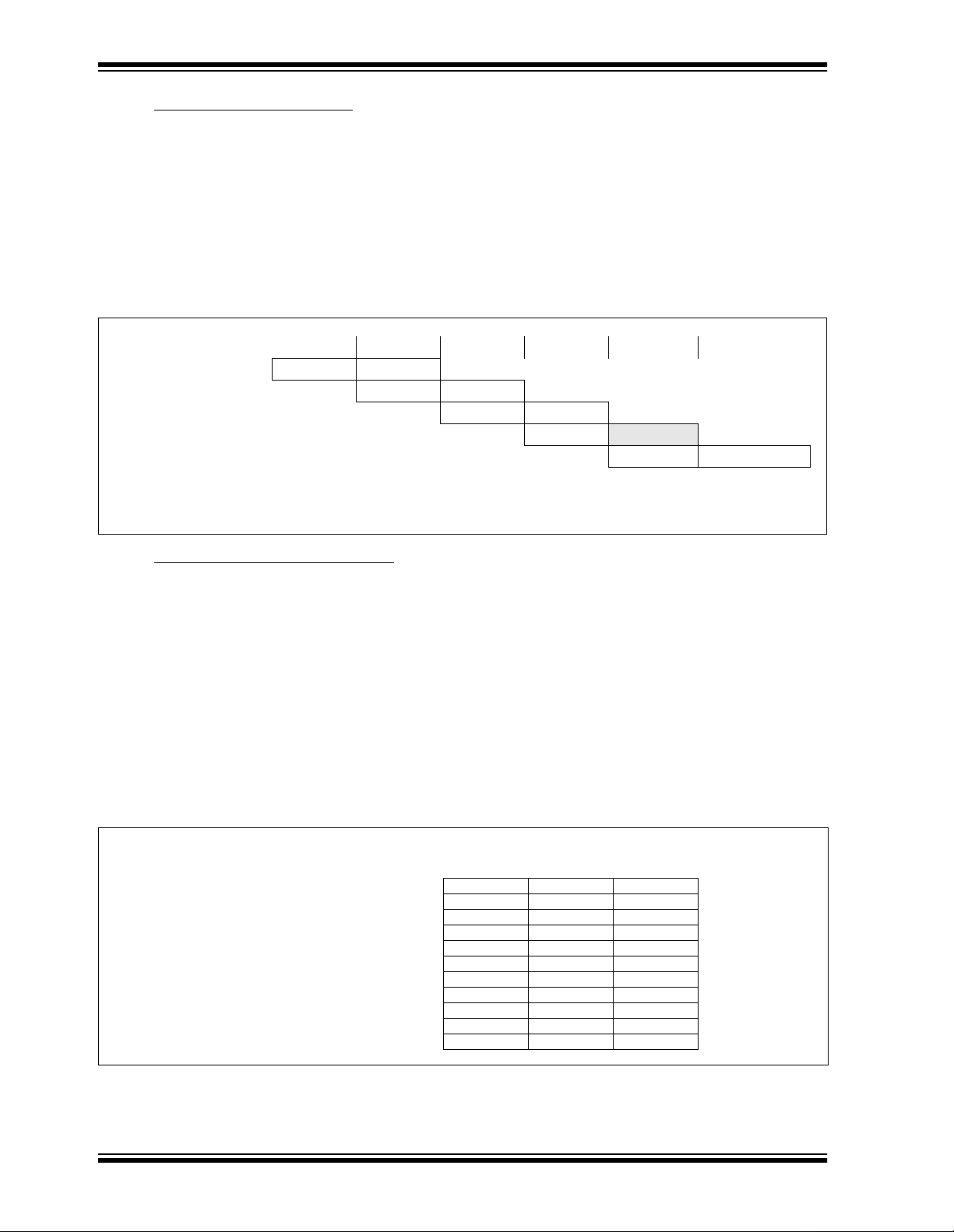
PIC18CXX2
4.6 Instruction Flow/Pipelining
A fetch cycle begins with the program counter (PC)
incrementing in Q1.
An “Instruction Cycle” consists of four Q cycles (Q1,
Q2, Q3 and Q4). The instruction fetch and execute are
pipelined such that fetch takes one instruction cycle
while decode and execute takes another instruction
cycle. However, due to the pipelining, each instruction
effectively executes in one cycle. If an instruction
causes the program counter to change (e.g. GOTO)
In the ex ecu tion cy cle, t he f etched i nstruction i s latche d
into the “Instruction Register" (IR) in cycle Q1. This
instruction is then decoded and executed during the
Q2, Q3, and Q4 cycles . Data memory is read during Q2
(operand read) and written during Q4 (destination
write).
then two cycles ar e required to complete the instruction
(Example 4-2).
EXAMPLE 4-2: INSTRUCTION PIPELINE FLOW
Tcy0 Tcy1 Tcy2 Tcy3 Tcy4 Tcy5
1. MOVLW 55h
2. MOVWF PORTB
3. BRA SUB_1
4. BSF PORTA, BIT3 (Forced NOP)
5. Instruction @ address SUB_1
All instructions are single cycle, except for any program branches. These take two cycles since the fetch
instruction is “flushed” from the pipeline while the new instruction is being fetched and then executed.
Fetch 1 Execute 1
Fetch 2 Execute 2
Fetch 3 Execute 3
Fetch 4 Flush
Fetch SUB_1 Execute SUB_1
4.7 Instructions in Program Memory
boundaries, the data contained in the instruction is a
word address. The word address is written to
The program memory is addressed in bytes. Instructions are stored as two bytes or four bytes in program
memory. The least significant byte of an instruction
word is always stored in a program memory location
with an even address (LSB = ’0’). Figure 4-5 shows an
example of ho w in struction w ords a re sto red in th e program memory. To maintain alignment with instruction
boundaries, the PC increments in steps of 2 and the
LSB will always read ’0’. (See Section 4.4)
The CALL and GOTO instructions have an absolute
PC<20:1>, which accesses the desired byte address
in program memory. Instruction #2 in Figure 4-5
shows how the instruction "GOTO 000006h’ is
encoded in the program memory. Program branch
instructions which encode a relative address offset
operate in the same manner. The offset value stored
in a branch instruction represents the number of single word instructions that the PC will be offset by.
Section 19.0 provides further details of the instruction
set.
program memory address embedded in to the instruction. Since instructions are always stored on word
FIGURE 4-5: INSTRUCTIONS IN PROGRAM MEMORY
Program Memory
Byte Locations
Instruction 1: MOVLW 055h 0Fh 55h 000008h
Instruction 2: GOTO 000006h EFh 03h 00000Ah
Instruction 3: MOVFF 123h, 456h C1h 23h 00000Eh
→
LSB = 1 LSB = 0
F0h 00h 00000Ch
F4h 56h 000010h
Word Address
↓
000000h
000002h
000004h
000006h
000012h
000014h
DS39026B-page 38 Preliminary
7/99 Microchip Technology Inc.

PIC18CXX2
4.7.1 TWO-WORD INSTRUCTIONS The PIC18CXX2 de vic es ha v e 4 tw o-w ord in structions :
MOVFF, CALL, GOTO and LFSR. The second word of
these instructions has the 4 MSB’s set to 1’s and is a
special kind o f NOP in structi on. The lower 12 bits o f th e
second word con tain data to be used b y the instructio n.
If the first word of the instruction is executed, the data
in the second word is accessed. If the second word of
the instruction is executed by itself (first word was
skipped), it will execute as a NOP. This action is neces-
sary when the two word instruction is preceded by a
conditional instructio n that changes the PC. A progr am
example that demonstrates this concept is shown in
Example 4-3. Refer to Sect ion 19.0 f or further details of
the instruction set.
EXAMPLE 4-3: TWO-WORD INSTRUCTION S
CASE 1:
Object code Source Code
0110 0110 0000 0000 TSTFSZ REG1 ; is RAM location 0?
1100 0001 0010 0011 MOVFF REG1, REG2 ; No, execute 2-word instruction
1111 0100 0101 0110 ; 2nd operand holds address of REG2
0010 0100 0000 0000 ADDWF REG3 ; continue code
CASE 2:
Object code Source Code
0110 0110 0000 0000 TSTFSZ REG1 ; is RAM location 0?
1100 0001 0010 0011 MOVFF REG1, REG2 ; Yes
1111 0100 0101 0110 ; 2nd operand becomes NOP
0010 0100 0000 0000 ADDWF REG3 ; continue code
4.8 Lookup Tables
4.8.2 TABLE READS/TABLE WRITES
Look-up tables are implemented two ways. These are:
• Computed GOTO
•Table Reads
4.8.1 COMPUTED GOTO A computed GOTO is accomplished by adding an offset
to the program counter (ADDWF PCL).
A lookup table can be formed with an ADDWF PCL
instruction and a group of RETLW 0xnn instructions.
WREG is loaded with an offset into the table before
executing a call to that table. The first instruction of the
called routine is the ADDWF PCL instruction. The next
instruction executed will be one of the RETLW 0xnn
instructions that returns the value 0xnn to the calling
function.
The offset va lue (v alue in WR EG) specifie s the n umber
of bytes that the program counter should advance.
In this method, only one data byte may be stored in
each instruction location and room on the return
address stack is required.
A better method of storing data in program memory
allows 2 bytes of data to be stored in each instruction
location.
Lookup table data may be stored 2 bytes per program
word by u si ng ta ble reads and writes. The tab le pointer
(TBLPTR) specifies the byte address and the table
latch (TABLAT) contains the data that is read from or
written to program memory. Data is transferred to/from
program memory one byte at a time.
A description of the Table Read/Table Write operation
is shown in Section 5.0.
7/99 Microchip Technology Inc.
Preliminary DS39026B-page 39

PIC18CXX2
4.9 Data Memory Organization
The data memory is implemented as static RAM. Each
register in the data memory has a 12-bit address,
allowing up to 4096 bytes of data memory. Figure 4-6
and Figure 4-7 show the data memory organization for
the PIC18CXX2 devices.
Banking is required to allo w more than 256 bytes to be
accessed. T he data memory map is divided into as
many as 16 banks that contain 256 bytes each. The
lower 4 bits of the Bank Select Register (BSR<3:0>)
select which bank will be accessed. The upper 4 bits
for the BSR are not implemented.
The data memory contains Special Function Registers
(SFR) and General Purpose Registers (GPR). The
SFRs are used for control and status of the controller
and peripheral functio ns , whi le GPRs are us ed f o r data
storage and scratch pad operations in the user’s application. The SFRs start at the last location of Bank 15
(OxFFF) and grow downwards. Any remaining space
beyond the SFRs in th e Bank may be im plem ent ed as
GPRs. GPRs start at the first location of Bank 0 and
grow upw ards. An y read o f an unimpl emented l ocation
will read as ’0’s.
The entire data memory may be accessed directly or
indirectly. Direct addressing may require the use of the
BSR register. Indirect addressing requires the use of
the File Select Register (FSR). Each FSR holds a 12bit address value that can be used to access any location in the Data Memory map without banking.
The instruction set and architecture allow operations
across all banks . This ma y be accomp lished b y indirect
addressing or by the use of the MOVFF instruction.
The MOVF F instructi on is a tw o word/tw o cycle instruction that moves a value from one register to another.
To ensure that commonly used registers (SFRs and
select GPRs) can be accesse d in a singl e cycle regardless of the current BSR values, an Access Bank is
implemented. A segment of Bank 0 and a segment of
Bank 15 comprise the Acc ess RAM . Section 4.10 provides a detailed description of the Access RAM.
4.9.2 SPECIAL FUNCTION REGISTERS The Special Function Registers (SFRs) are registers
used by the C PU and P eripheral M odules f or controlling
the desired oper ation of the de vic e. These re gisters are
implemented as static RAM. A list of these registers is
given in Table 4-1 and Table 4-2.
The SFRs can be classified into two sets; those associated with the “core” function and those related to the
peripheral functions. Those registers related to the
“core” are described in this s ection , while thos e relate d
to the operation of the peripheral features are
described in the section of that peripheral feature.
The SFRs are typically distrib uted amon g the peripherals whose functions they control.
The unused SFR locations will be unimplemented and
read as '0's. See Table 4-1 for addresses f or the SFRs .
4.9.1 GENERAL PURPOSE REGISTER FILE The register file can be ac cess ed eith er direct ly or indi-
rectly. Indirect addressing operates through the File
Select Registers (FSR). The operation of indirect
addressing is shown in Section 4.12.
Enhanced MCU devices may have banked memory in
the GPR area. GPRs are not initialized by a Power-on
Reset and are unchanged on all other resets.
Data RAM is available for use as GPR registers by all
instructi ons. T he top ha lf of ban k 15 (0xF 80 to 0xFF F)
contains SFRs. All other banks of data memory contain
GPR registers starting with bank 0.
DS39026B-page 40 Preliminary
7/99 Microchip Technology Inc.

FIGURE 4-6: DATA MEMORY MAP FOR PIC18C242/442
PIC18CXX2
BSR<3:0>
= 0000b
= 0001b
= 0010b
= 1110b
= 1111b
When a = 1,
the BSR is used to specify
the RAM location that the
instruction uses.
Bank 0
Bank 1
Bank 2
to
Bank 14
Bank 15
Data Memory Map
00h
Access RAM
FFh
00h
FFh
Unused
Read ’00h’
00h
FFh
Unused
GPR
GPR
SFR
000h
07Fh
080h
0FFh
100h
1FFh
200h
EFFh
F00h
F7Fh
F80h
FFFh
Access Bank
Access RAM low
Access RAM high
(SFR’s)
When a = 0,
the BSR is ignored and the
Access Bank is used.
The first 128 bytes are
General Purpose RAM
(from Bank 0).
The second 128 bytes are
Special Function Registers
(from Bank 15).
00h
7Fh
80h
FFh
7/99 Microchip Technology Inc.
Preliminary DS39026B-page 41
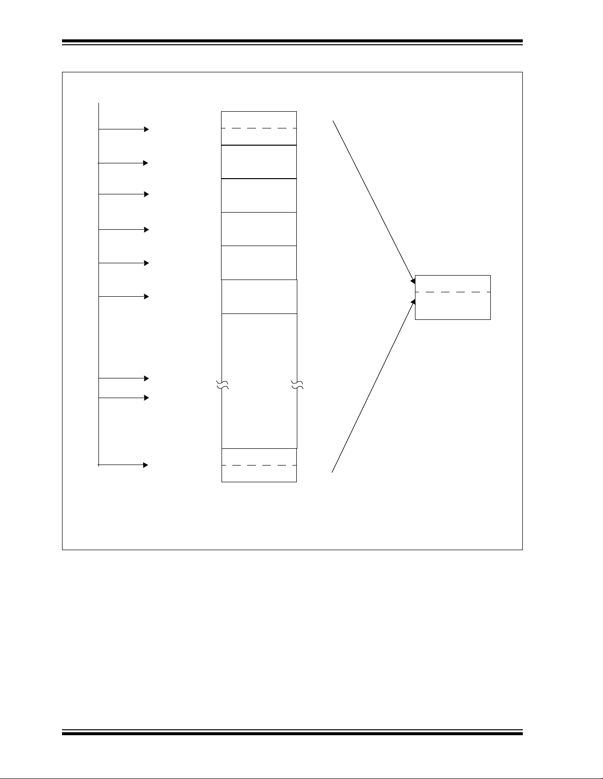
PIC18CXX2
FIGURE 4-7: DATA MEMORY MAP FOR PIC18C252/452
BSR<3:0>
= 0000b
= 0001b
= 0010b
= 0011b
= 0100b
= 0101b
= 0110b
= 1110b
= 1111b
When a = 1,
the BSR is used to specify
the RAM location that the
instruction uses.
Bank 0
Bank 1
Bank 2
Bank 3
Bank 4
Bank 5
Bank 6
to
Bank 14
Bank 15
Data Memory Map
00h
Access RAM
FFh
00h
FFh
00h
FFh
00h
FFh
00h
FFh
00h
FFh
GPR
GPR
GPR
GPR
GPR
GPR
Unused
Read ’00h’
Unused
SFR
000h
07Fh
080h
0FFh
100h
1FFh
200h
2FFh
300h
3FFh
400h
4FFh
500h
5FFh
600h
EFFh
F00h
F7Fh
F80h
FFFh
Access Bank
Access RAM low
Access RAM high
(SFR’s)
When a = 0,
the BSR is ignored and the
Access Bank is used.
The first 128 bytes are
General Purpose RAM
(from Bank 0).
The second 128 bytes are
Special Function Registers
(from Bank 15).
00h
7Fh
80h
FFh
DS39026B-page 42 Preliminary
7/99 Microchip Technology Inc.

TABLE 4-1: SPECIAL FUNCTION REGISTER MAP
PIC18CXX2
FFFh TOSU FDFh
FFEh TOSH FDEh
FFDh TOSL FDDh
FFCh STKPTR FDCh
FFBh PCLATU FDBh
(3)
INDF2
POSTINC2
POSTDEC2
PREINC2
PLUSW2
(3)
(3)
FBFh CCPR1H F9Fh IPR1
(3)
FBEh CCPR1L F9Eh PIR1
(3)
FBDh CCP1CON F9Dh PIE1
FBCh CCPR2H F9Ch —
FBBh CCPR2L F9Bh —
FFAh PCLATH FDAh FSR2H FBAh CCP2CON F9Ah —
FF9h PCL FD9h FSR2L FB9h — F99h —
FF8h TBLPTRU FD8h STATUS FB8h — F98h —
FF7h TBLPTRH FD7h TMR0H FB7h — F97h —
FF6h TBLPTRL FD6h TMR0L FB6h — F96h
FF5h TABLAT FD5h T0CON FB5h — F95h
TRISE
TRISD
FF4h PRODH FD4h — FB4h — F94h TRISC
FF3h PRODL FD3h OSCCON FB3h TMR3H F93h TRISB
FF2h INTCON FD2h LVDCON FB2h TMR3L F92h TRISA
FF1h INTCON2 FD1h WDTCON FB1h T3CON F91h —
FF0h INTCON3 FD0h RCON FB0h — F90h —
FEFh
FEEh
FEDh
FECh
FEBh
(3)
INDF0
POSTINC0
POSTDEC0
PREINC0
PLUSW0
(3)
FCFh TMR1H FAFh SPBRG F8Fh —
(3)
FCEh TMR1L FAEh RCREG F8Eh —
(3)
FCDh T1CON FADh TXREG F8Dh
(3)
FCCh TMR2 FACh TXSTA F8Ch
FCBh PR2 FABh RCSTA F8Bh LATC
LATE
LATD
FEAh FSR0H FCAh T2CON FAAh — F8Ah LATB
FE9h FSR0L FC9h SSPBUF FA9h — F89h LATA
FE8h WREG FC8h SSPADD FA8h — F88h —
FE7h
FE6h
FE5h
FE4h
FE3h
(3)
INDF1
POSTINC1
POSTDEC1
PREINC1
PLUSW1
(3)
FC7h SSPSTAT FA7h — F87h —
(3)
FC6h SSPCON1 FA6h — F86h —
(3)
FC5h SSPCON2 FA5h — F85h —
(3)
FC4h ADRESH FA4h — F84h
FC3h ADRESL FA3h — F83h
PORTE
PORTD
FE2h FSR1H FC2h ADCON0 FA2h IPR2 F82h PORTC
FE1h FSR1L FC1h ADCON1 FA1h PIR2 F81h PORTB
FE0h BSR FC0h — FA0h PIE2 F80h PORTA
(2)
(2)
(2)
(2)
(2)
(2)
Note 1: Unimplemented registers are read as ’0’
2: This registers is not available on PIC18C2X2 devices
3: This is not a physical register
7/99 Microchip Technology Inc.
Preliminary DS39026B-page 43

PIC18CXX2
TABLE 4-2: REGISTER FILE SUMMARY
Value on
Filename Bit 7 Bit 6 Bit 5 Bit 4 B it 3 Bit 2 Bit 1 Bit 0
POR,
BOR
TOSU — — — Top-of-Stack upper Byte (TOS<20:16>) ---0 0000 ---0 0000
TOSH Top-of-Stack High Byte (TOS<15:8>) 0000 0000 0000 0000
TOSL Top-of-Stack Low Byte (TOS<7:0>) 0000 0000 0000 0000
STKPTR STKFUL STKUNF
PCLATU
PCLATH Holding Register for PC<15:8> 0000 0000 0000 0000
PCL PC Low Byte (PC<7:0>) 0000 0000 0000 0000
TBLPTRU
TBLPTRH Program Memory Table Pointer High Byte (TBLPTR<15:8>) 0000 0000 0000 0000
TBLPTRL Program Memory Table Pointer Low Byte (TBLPTR<7:0>) 0000 0000 0000 0000
TABLAT Program Memory Table Latch 0000 0000 0000 0000
PRODH Product Register High Byte xxxx xxxx uuuu uuuu
PRODL Product Register Low Byte xxxx xxxx uuuu uuuu
INTCON GIE/GIEH PEIE/GIEL TMR0IE INT0IE RBIE TMR0IF INT0IF RBIF 0000 000x 0000 000u
INTCON2 RBPU INTEDG0 INTEDG1 INTEDG2
INTCON3 INT 2IP INT1IP
INDF0 Uses contents of FSR0 to address data memory - value of FSR0 not changed (not a physical register) n/a n/a
POSTINC0 Uses contents of FSR0 to address data memory - value of FSR0 post-incremented (not a physical register) n/a n/a
POSTDEC0 Uses contents of FSR0 to address data memory - value of FSR0 post-decremented (not a physical register) n/a n/a
PREINC0 Uses contents of FSR0 to address data memory - value of FSR0 pre-incremented (not a physical register) n/a n/a
PLUSW0 Uses contents of FSR0 to address data memory - value of FSR0 pre-incremented (not a physical register) -
FSR0H
FSR0L Indirect Data Memory Address Pointer 0 Low Byte xxxx xxxx uuuu uuuu
WREG Working Register xxxx xxxx uuuu uuuu
INDF1 Uses contents of FSR1 to address data memory - value of FSR1 not changed (not a physical register) n/a n/a
POSTINC1 Uses contents of FSR1 to address data memory - value of FSR1 post-incremented (not a physical register) n/a n/a
POSTDEC1 Uses contents of FSR1 to address data memory - value of FSR1 post-decremented (not a physical register) n/a n/a
PREINC1 Uses contents of FSR1 to address data memory - value of FSR1 pre-incremented (not a physical register) n/a n/a
PLUSW1 Uses contents of FSR1 to address data memory - value of FSR1 pre-incremented (not a physical register) -
FSR1H
FSR1L Indirect Data Memory Address Pointer 1 Low Byte xxxx xxxx uuuu uuuu
BSR
INDF2 Uses contents of FSR2 to address data memory - value of FSR2 not changed (not a physical register) n/a n/a
POSTINC2 Uses contents of FSR2 to address data memory - value of FSR2 post-incremented (not a physical register) n/a n/a
POSTDEC2 Uses contents of FSR2 to address data memory - value of FSR2 post-decremented (not a physical register) n/a n/a
PREINC2 Uses contents of FSR2 to address data memory - value of FSR2 pre-incremented (not a physical register) n/a n/a
PLUSW2 Uses contents of FSR2 to address data memory - value of FSR2 pre-incremented (not a physical register) -
FSR2H
FSR2L Indirect Data Memory Address Pointer 2 Low Byte xxxx xxxx uuuu uuuu
STATUS
TMR0H Timer0 register high byte 0000 0000 0000 0000
TMR0L Timer0 register low byte xxxx xxxx uuuu uuuu
T0CON TMR0ON T08BIT T0CS T0SE PSA T0PS2 T0PS1 T0PS0 1111 1111 1111 1111
— — — Holdi ng Regi st er for PC<20:16 > ---0 0000 ---0 0000
— —
value of FSR0 offset by value in WREG
— — — — Indirect Data Memory Address Pointer 0 High Byte ---- 0000 ---- 0000
value of FSR1 offset by value in WREG
— — — — Indirect Data Memory Address Pointer 1 High Byte ---- 0000 ---- 0000
— — — — Bank Select Register ---- 0000 ---- 0000
value of FSR2 offset by value in WREG
— — — — Indirect Data Memory Address Pointer 2 High Byte ---- 0000 ---- 0000
— — —N OV Z DC C ---x xxxx ---u uuuu
— Return Stack Pointer 00-0 0000 00-0 0000
(2)
bit21
Program Memory Table Pointe r Upper Byte (TBLPTR<20:16>) ---0 0000 ---0 0000
—TMR0IP —RBIP 1111 -1-1 1111 -1-1
— INT2IE INT1IE —INT2IFINT1IF11-0 0-00 11-0 0-00
n/a n/a
n/a n/a
n/a n/a
Value on
all other
resets
(note 3)
Legend: x = unknown, u = unchanged, - = unimplemented, q = value depends on condition
Note1: RA6 and associated bits are configured as port pins in RCIO and ECIO oscillator mode only and read ’0’ in all
other oscillator modes.
2: Bit 21 of the TBLP TRU allows access to the device configuration bits.
3: Other (non-power-up) resets include external reset through MCLR
and Watchdog Timer Reset.
DS39026B-page 44 Preliminary
7/99 Microchip Technology Inc.
TABLE 4-2: REGISTER FILE SUMMARY (Cont.’d)
PIC18CXX2
Filename Bit 7 Bit 6 Bit 5 Bit 4 Bit 3 Bit 2 Bit 1 Bit 0
POR,
BOR
OSCCON — — — — — — —SCS ---- ---0 ---- ---0
Value on
LVDCON
WDTCON
RCON IPEN LWRT
TMR1H Timer1 Register High Byte xxxx xxxx uuuu uuuu
TMR1L Timer1 Register Low Byte xxxx xxxx uuuu uuuu
T1CON RD16
TMR2 Timer2 Register 0000 0000 0000 0000
PR2 Timer2 Period Register 1111 1111 1111 1111
T2CON
SSPBUF SSP Receive Buffer/Transmit Register xxxx xxxx uuuu uuuu
SSPADD
SSPSTAT SMP CKE D/A
SSPCON1 WCOL SSPOV SSPEN CKP SSPM3 SSPM2 SSPM1 SSPM0 0000 0000 0000 0000
SSPCON2 GCEN ACKSTAT ACKDT ACKEN RCEN PEN RSEN SEN 0000 0000 0000 0000
ADRESH A/D Result Register High Byte xxxx xxxx uuuu uuuu
ADRESL A/D Result Register Low Byte xxxx xxxx uuuu uuuu
ADCON0 ADCS1 ADCS0 CHS2 CHS1 CHS0 GO/DONE
ADCON1 ADFM ADCS2
CCPR1H Capture/Compare/PWM Register1 High Byte xxxx xxxx uuuu uuuu
CCPR1L Capture/Compare/PWM Register1 Low Byte xxxx xxxx uuuu uuuu
CCP1CON
CCPR2H Capture/Compare/PWM Register2 High Byte xxxx xxxx uuuu uuuu
CCPR2L Capture/Compare/PWM Register2 Low Byte xxxx xxxx uuuu uuuu
CCP2CON
TMR3H Timer3 Register High Byte xxxx xxxx uuuu uuuu
TMR3L Timer3 Register Low Byte xxxx xxxx uuuu uuuu
T3CON RD16 T3CCP2 T3CKPS1 T3CKPS0 T3CCP1 T3SYNC TMR3CS TMR3ON 0000 0000 uuuu uuuu
SPBRG USART1 Baud Rate Generator 0000 0000 0000 0000
RCREG USART1 Receive Register 0000 0000 0000 0000
TXREG USART1 Transmit Register 0000 0000 0000 0000
TXSTA CSRC TX9 TXEN SYNC
RCSTA SPEN RX9 SREN CREN ADDEN FERR OERR RX9D 0000 000x 0000 000x
— — IRVST LVDEN LVDL3 LVDL2 LVDL1 LVDL0 --00 0101 --00 0101
— — — — — — —SWDTE---- ---0 ---- ---0
—RI TO PD POR BOR 0q-1 11qq 0q-q qquu
— T1CKPS1 T1CKPS0 T1OSCEN T1SYNC TMR1CS TMR1ON 0-00 0000 u-uu uuuu
— TOUTPS3 TOUTPS2 TOUTPS1 TOUTPS0 TMR2ON T2CKPS1 T2CKPS0 -000 0000 -000 0000
2
SSP Address Register in I
— — DC1B1 DC1B0 CCP1M3 CCP1M2 CCP1M1 CCP1M0 --00 0000 --00 0000
— — DC2B1 DC2B0 CCP2M3 CCP2M2 CCP2M1 CCP2M0 --00 0000 --00 0000
C Slave Mode. SSP Baud Rate Reload Register in I2C Master Mode.
PSR/WUA BF 0000 0000 0000 0000
—ADON0000 00-0 0000 00-0
— — PCFG3 PCFG2 PCFG1 PCFG0 00-- 0000 00-- 0000
— BRGH TRMT TX9D 0000 -010 0000 -010
0000 0000 0000 0000
Val ue on
all other
resets
(note 3)
Legend: x = unknown, u = unchanged, - = unimplemented, q = value depends on condition
Note1: RA6 and associated bits are configured as port pins in RCIO and ECIO oscillator mode only and read ’0’ in all
other oscillator modes.
2: Bit 21 of the TBLP TRU allows access to the device configuration bits.
3: Other (non-power-up) resets include external reset through MCLR
and Watchdog Timer Reset.
7/99 Microchip Technology Inc.
Preliminary DS39026B-page 45
PIC18CXX2
TABLE 4-2: REGISTER FILE SUMMARY (Cont.’d)
Value on
Filename Bit 7 Bit 6 Bit 5 Bit 4 B it 3 Bit 2 Bit 1 Bit 0
IPR2 — — — — BCLIP LVDIP TMR3IP CCP2IP ---- 1111 ---- 1111
PIR2
PIE2
IPR1 PSPIP ADIP R CIP TXIP SSPIP CCP1IP TMR2IP TMR1IP 1111 1111 1111 1111
PIR1 PSPIF ADIF RCIF TXIF SSPIF CCP1IF TMR2IF TMR1IF 0000 0000 0000 0000
PIE1 PSPIE ADIE RCIE TXIE SSPIE CCP1IE TMR2IE TMR1IE 0000 0000 0000 0000
TRISE IBF OBF IBOV PSP-
TRISD Data Direction Control Register for PORTD 1111 1111 1111 1111
TRISC Data Direction Control Register for PORTC 1111 1111 1111 1111
TRISB Data Direction Control Register for PORTB 1111 1111 1111 1111
TRISA
LATE
LATD Read PORTD Data Latch, Write PORTD Data Latch xxxx xxxx uuuu uuuu
LATC Read PORTC Data Latch, Write PORTC Data Latch xxxx xxxx uuuu uuuu
LATB Read PORTB Data Latch, Write PORTB Data Latch xxxx xxxx uuuu uuuu
LATA
PORTE Read PORTE pins, Write PORTE Data Latch ---- -000 ---- -000
PORTD Read PORTD pins, Write PORTD Data Latch xxxx xxxx uuuu uuuu
PORTC Read PORTC pins, Write PORTC Data Latch xxxx xxxx uuuu uuuu
PORTB Read PORTB pins, Write PORTB Data Latch xxxx xxxx uuuu uuuu
PORTA
— — — — BCLIF LVDIF TMR3IF CCP2IF ---- 0000 ---- 0000
— — — — BCLIE LVDIE TMR3IE CCP2IE ---- 0000 ---- 0000
MODE
—
— — — — — Read PORTE Data Latch, Write
—
—
TRISA6
LATA6
(1)
RA6
(1)
Data Direction Control Regi st er for PORTA -111 1111 -111 1111
(1)
Read PORTA Data Latch, Write PORTA Data Latch
Read PORTA pins, Write PORTA Data Latch
— Data Direction bits for PORTE 0000 -111 0000 -111
PORTE Data Latch
(1)
(1)
POR,
BOR
---- -xxx ---- -uuu
-xxx xxxx -uuu uuuu
-x0x 0000 -u0u 0000
Value on
all other
resets
(note 3)
Legend: x = unknown, u = unchanged, - = unimplemented, q = value depends on condition
Note1: RA6 and associated bits are configured as port pins in RCIO and ECIO oscillator mode only and read ’0’ in all
other oscillator modes.
2: Bit 21 of the TBLP TRU allows access to the device configuration bits.
3: Other (non-power-up) resets include external reset through MCLR
and Watchdog Timer Reset.
4.10 Access Bank
A bit in the instruction word specifies if the operation is
to occur in the bank specified by the BSR register or in
The Access Bank is an architectural enhancement
which is very useful for C compiler code optimization.
The techniques used by the C compiler may also be
useful for programs written in assembly.
This data memory region can be used for:
• Intermediate computational values
• Local variables of subrou tines
• Faster context saving/switching of variables
• Common variab le s
the Access Bank. This bit is denoted by the ’a’ bit (for
access bit).
When forced in the Access Bank (a = ’0’), the last
address in Access RAM Low is followed by the first
address in Access RAM High. Access RAM High maps
the Special Function registers so that these registers
can be accessed without any software overhead. This
is useful for testing status flags and modifying control
bits.
• Faster evaluation/control of SFRs (no banking)
The Access Bank is comprised of the upper 128 bytes
in Bank 15 (SFRs) and the lower 128 bytes in Bank 0.
These two sections will be referred to as Access RAM
High and Access RAM Low, respectively. Figure 4-6
and Figure 4-7 indicate the Access RAM areas.
DS39026B-page 46 Preliminary
7/99 Microchip Technology Inc.
PIC18CXX2
4.11 Bank Select Regist er (BS R)
The need for a large general purpose memory space
dictates a RAM banking scheme. The data memory is
partitioned into sixteen banks. When using direct
addressing, the BSR should be configured for the
desired bank.
BSR<3:0> holds the upper 4 bits of the 12-bit RAM
address. The BSR<7:4> bits will always read ’0’s, and
writes will have no effect.
MOVLB instruction has bee n provided in the instruc-
A
tion set to assist in selecting banks.
FIGURE 4-8: DIRECT ADDRESSING
Direct Addressing
from opcode
(3)
bank select
BSR<3:0> 7
(2)
location select
(3)
If the currently selected bank is not implemented, any
read will return all '0's and all writes are ignored. The
STAT U S regis ter bi ts will be set/cleared as appropriate
for the instruction performed.
Each Bank extends up to FFh (256 bytes). All data
memory is implement ed as static RAM.
A MOVFF i nstruction ignores the BSR , si nc e th e 1 2-b it
addresses are embedded into the instruction word.
Section 4.12 provides a d escription of ind irect address ing, whic h allows lin ear add ressing o f the ent ire RAM
space.
0
00h 01h 0Eh 0Fh
000h
100h
E00h
F00h
Data
Memory
(1)
0FFh
1FFh
EFFh
Bank 0 Bank 1 Bank 14 Bank 15
Note 1: For register file map detail, see Table 4-1.
2: The access bit of the instruction can be used to force an override of the selected bank
(BSR<3:0>) to the registers of the Access Bank.
3: The MOVFF instruction embeds the entire 12-bit address in the instruction.
FFFh
7/99 Microchip Technology Inc.
Preliminary DS39026B-page 47

PIC18CXX2
4.12 Indirect Addressing, INDF and FSR Registers
Indirect addressin g is a mode of addr essing data mem ory, where the data memory address in the instruction
is not fixed. An SF R re gister is used as a pointer to th e
data memory location that is to be read or written.
Since this pointer is in RAM, the contents can be modified by the program. This can be useful for data tables
in the data memory and for so ftware stac ks . Figu re 4-9
shows the operati on of indirect addressing . This sho ws
the moving of the value to the data memory address
specified by the value of the FSR register.
Indirect addressing is possible by using one of the
INDF registers. Any instruction using the INDF register
actually accesses the register pointed to by the File
Select Register, FSR. Reading the INDF register itself
indirectly (FSR = ’0’) will read 00h. Writing to the INDF
register indirectly results in a no-operation. The FSR
register contains a 12-bit address, which is shown in
Figure 4-10.
The INDFn register is not a physical register. Addressing INDFn actually addresses the register whose
address is contained in the FSRn register (FSRn is a
pointer). T his is indirect addressing.
Example 4-4 shows a simple use of indirect addressing
to clear the RAM in Bank1 (locations 100h-1FFh) in a
minimum number of instructions.
EXAMPLE 4-4: HOW TO CLEAR RAM
(BANK1) USING INDIRECT
ADDRESSING
LFSR 0x100, FSR0 ;
NEXT CLRF POSTINC0 ; Clear INDF register
; & inc pointer
BTFSS FSR0H, 1 ; All done w/ Bank1?
GOTO NEXT ; NO, clear next
CONTINUE ;
: ; YES, continue
There are three indirect addressing registers. To
address the entire data memory space (4096 bytes),
these registers are 12-bit wide. To store the 12-bits of
addressing information, two 8-bit registers are
required. These indirect addres si ng regi ste r s are:
1. FSR0: composed of FSR0H:FSR0L
2. FSR1: composed of FSR1H:FSR1L
3. FSR2: composed of FSR2H:FSR2L
In addition, there are registers INDF0, INDF1 and
INDF2, which are not physically implemented. Reading
or writing to these registers activates indirect addressing, with the value in the corresponding FSR register
being the address of the data.
If an instruction writes a value to INDF0, the value will
be written to the add res s poi nte d t o b y F S R0H:FSR 0 L.
A read from INDF1 reads the data from the address
pointed t o by FSR1H:FSR1L. INDFn can be us ed in
code anywhere an operand can be used.
If INDF0, I NDF1 or INDF2 are re ad indirectly via an
FSR, all ’0’s are read (zero bit is set). Similarly, if
INDF0, INDF1 or INDF2 are written to indirectly, the
operation will be equiv alent to a NOP instruction and the
STATUS bits are not affected.
4.12.1 INDIRECT ADDRESSING OPERATION Each FSR register has an INDF register associated
with it, plus four additional register addresses. Performing an operation on one of these five registers
determines how the FSR will be modified during indirect addres sing.
When data access is done to one of the five INDFn
locations, the address selected will configure the FSRn
register to:
• Do nothing to FSRn after an indirect access (no
change) - INDFn
• Auto-decrement FSRn after an indirect access
(post-decrement) - POSTDECn
• Auto-increment FSRn after an indirect access
(post-increment) - POSTINCn
• Auto-increment FSRn before an indirect access
(pre-increment) - PREINCn
• Use the value in the WREG register as an offset
to FSRn. Do not modify the v alue of the W REG or
the FSRn register after an indirect access (no
change) - PLUSWn
When using the auto-increment or auto-decrement
features, the effect on the FSR is no t reflecte d in the
STATUS register. For example, if the indir ect a ddress
causes the FSR to equal '0' , the Z bit will not be set.
Incrementing or decrementing an FSR affects all 12
bits. That is, when FSRnL overflow s from an increment,
FSRnH will be incremented automatically.
Adding these fe atures allo ws the FSR n to be used as a
stack pointer in addition to its uses for table operations
in data memory.
Each FSR has an address associated with it that performs an inde xed indirect access. When a data acces s
to this INDFn location (PLUSWn) occurs, the FSRn is
configured to add the si gne d value in the WREG register and the value in FSR to form the add ress before an
indirect access. The FSR value is not changed.
If an FSR register contains a v alue tha t points to one of
the INDFn , an indirect re ad will read 00h (zero bit is
set), while an indirect write will be equivalent to a NOP
(STATUS bits are not affected).
If an indirect addressing operation is done where the
target address is an FSRnH or FSRnL register, the
write operation will dominate over the pre- or postincrement /decrement functions.
DS39026B-page 48 Preliminary
7/99 Microchip Technology Inc.
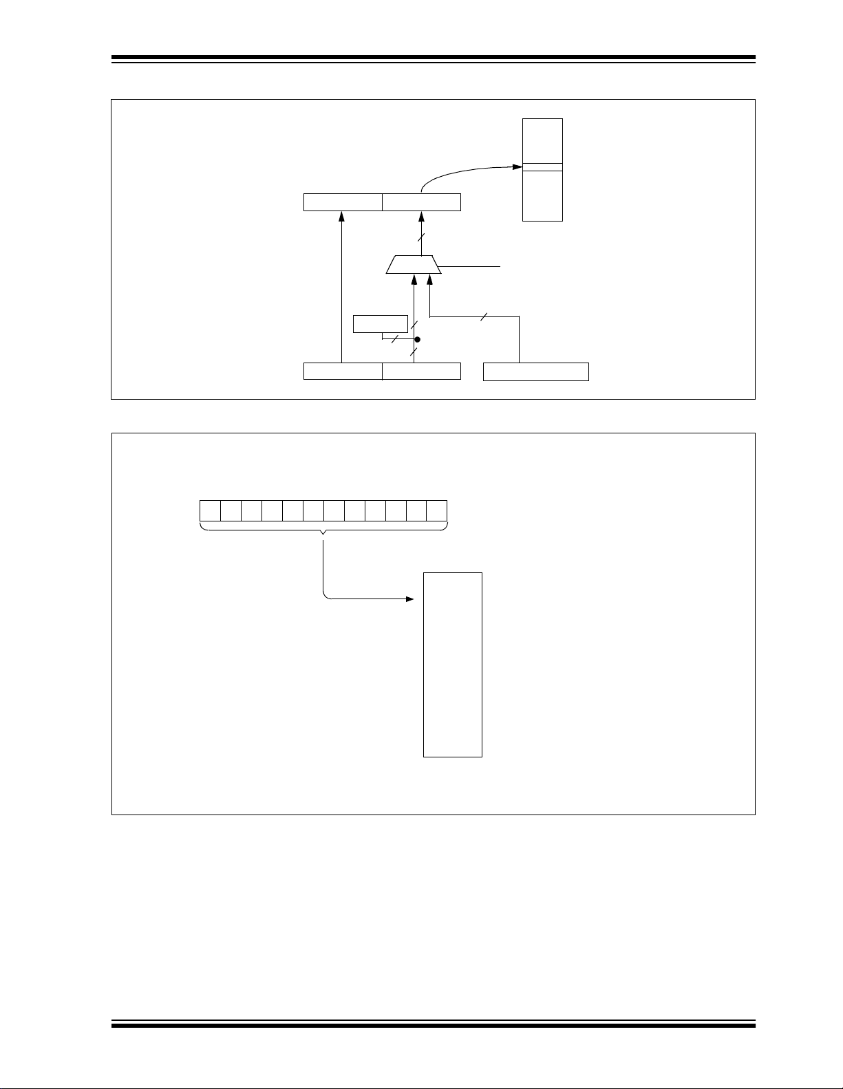
FIGURE 4-9: INDIRECT ADDRESSING OPERATION
Instruction
Executed
Opcode Address
12
File Address = access of an indirect addressing register
RAM
PIC18CXX2
0h
FFFh
BSR<3:0>
Instruction
Fetched
Opcode
4
FIGURE 4-10: INDIRECT ADDRESSING
Indirect Addressing
FSR register11
location select
Data
Memory
(1)
12
8
File
12
FSR
0
0000h
Note 1: For register file map detail, see Table 4-1.
7/99 Microchip Technology Inc.
0FFFh
Preliminary DS39026B-page 49

PIC18CXX2
4.13 STATUS Register
The STATUS register, shown in Register4-2, contains
the arithmetic status of the ALU. The STATUS register
can be the destination for any instruction, as with any
other register. If the STATUS register is the destination
for an instruction that affects the Z, DC, C, OV or N bits,
then the write to these five bits is disabled. These bits
are set or cleared a cc ord ing to t he device log ic. The r efore, th e r esult of an instructi on with th e STA TUS re gi ster as destination may be different than intended.
Register 4-2: STATUS Register
U-0 U-0 U-0 R/W-x R/W-x R/W-x R/W-x R/W-x
——— NOVZDCC
bit 7 bit 0
bit 7:5 Unimplemented: Read as ’0’
bit 4 N: Negative bit
This bit is used for sign ed arithmatic ( 2’ s complement). It indicates whether th e result was neg-
ative, (ALU MSB = 1)
1 = Result was negative
0 = Result was positive
bit 3 OV: Overflow bit
This bit is used f or signed arithmetic (2’s co mplement). It indi cates an ov erflow of the 7-bit magnitude, which causes the sign bit (bit7) to change state.
1 = Overflow occurred for signed arithmatic (in this arithmetic operation)
0 = No overflow occurre d
bit2 Z: Zero bit
1 = The result of an arithmetic or logic operation is zero
0 = The result of an arithmetic or logic operation is not zero
bit 1 DC: Digit carry/borrow
For ADDWF, ADDLW, SUBLW, and SUB WF instructions
1 = A carry-out from the 4th low order bit of the result occurred
0 = No carry-out from the 4th low order bit of the result
Note: For borrow
complement of the second operand. For rotate (RRF, RLF) instructions, this bit is
loaded with either the bit 4 or bit 3 of the source register.
bit 0 C: Carry/borrow bit
For ADDWF, ADDLW, SUBLW, and SUBWF instructions
1 = A carry-out from the most significant bit of the result occurred
0 = No carry-out from the most significant bit of the result occurred
Note: For borrow
complement of the second operand. For rotate (RRF, RLF) instructions, this bit is
loaded with either the high or low order bit of the source register.
bit
, the polarity is reversed. A subtraction is executed by adding the two’s
, the polarity is reversed. A subtraction is executed by adding the two’s
For example, CLRF STATUS will clear th e upp er -t h ree
bits and set th e Z bi t. T his l ea v es the STATUS register
as 000u u1uu (where u = unchanged).
It is recommended, therefore, that only BCF, BSF,
SWAPF, MOVFF and MOVWF instr uctions are used to
alter the STATUS register, because these instructions do not affect the Z, C, DC, OV or N bits from
the STATUS register. For other instructions not
affecting any status bits, see Table 19-2.
Note: The C and DC b its operat e as a bo rrow and
digit borrow
bit respectively, in subtraction.
Legend:
R = Readable bit W = Writable bit U = Unimplemented bit, read as ‘0’
- n = Value at POR reset ’1’ = Bit is set ’0’ = Bit is cleared x = Bit is unknown
DS39026B-page 50 Preliminary
7/99 Microchip Technology Inc.

PIC18CXX2
4.13.1 RCON REGISTER
The Reset Control (RCON) register contains flag bits,
that allow differentiation between the sources of a
device reset. T hese flags include t he TO, PD, POR,
and RI bits. This regis ter is readab le and writab le .
BOR
Register 4-3: RCON Register
R/W-0 R/W-0 U-0 R/W-1 R/W-1 R/W-1 R/W-0 R/W-0
IPEN LWRT
bit 7 bit 0
bit 7 IPEN: Interrupt Priority Enable bit
1 = Enable priority levels on interrupts
0 = Disable priority levels on interrupts (16CXXX compatibility mode)
bit 6 LWRT: Long Write Enable bit
1 = Enable TBLWT to internal program memory
Once this bit is set, it can only be cleared by a POR or MCLR
0 = Disable TBLWT to internal program memory; TBLWT only to external program memory
bit 5 Unimplemented: Read as ’0’
bit 4 RI
bit 3 TO
bit 2 PD
bit 1 POR
bit 0 BOR
: Reset Instruction Flag bit
1 = The Reset instruction was not executed
0 = The Reset instruction was executed causing a device reset
(must be set in software after a Brown-out Reset occurs)
: Watchdog Time-out Flag bit
1 = After power-up, CLRWDT instruction, or SLEEP instruction
0 = A WDT time-out occurred
: Power-down Detection Flag bit
1 = After power-up or by the CLRWDT instruction
0 = By execution of the SLEEP inst ruction
: Power-on Reset Status bit
1 = A Power-on Reset has not occurred
0 = A Power-on Reset occurred
(must be set in software after a Power-on Reset occurs)
: Brown-out Reset Status bit
1 = A Brown-out Reset has not occurred
0 = A Brown-out Reset occurred
(must be set in software after a Brown-out Reset occurs)
—RITO PD POR BOR
Note 1: If the BOREN conf iguration b it is set, BOR
is ’1’ on Power-on Reset. If the BOREN
configuration b it i s clea r, BOR
on Power-on Reset.
The BOR
not necessarily predictable if the brownout circuit is disabled (the BOREN configuration bit is clear). BO R
by the user and checked on subsequent
resets to see if it is clear, indicating a
brown-out has occurred.
2: It is recommended that the POR
after a Power-on Reset has been
detected, so that subsequent Power-on
Resets may be detected.
reset.
status bit is a "don 't care " and i s
is unknown
must then be set
bit be set
Legend:
R = Readable bit W = Writable bit U = Unimplemented bit, read as ‘0’
- n = Value at POR reset ’1’ = Bit is set ’0’ = Bit is cleared x = Bit is unknown
7/99 Microchip Technology Inc.
Preliminary DS39026B-page 51

PIC18CXX2
NOTES:
DS39026B-page 52 Preliminary
7/99 Microchip Technology Inc.

PIC18CXX2
5.0 TABLE READS/TABLE WRITES
Enhanced devices have two memory spaces: the program memory space and the data memory space. The
program memory space is 16 bits wide, while the data
memory spa ce is 8 bits wide. Table Reads and Table
Writes have been provided to move data between
these two memory spaces through an 8 bit register
(TABLAT).
The operations that allow the processor to move data
between the data and program memory spaces are:
•Table Read (TBLRD)
• Table Write (TBLWT)
FIGURE 5-1: TABLE READ OPERATION
TABLE POINTER
TBLPTRU
TBLPTRH TBLPTRL
(1)
PROGRAM MEMOR Y
Table Read operations retrieve data from program
memory and place it into the Data memory space.
Figure 5-1 shows the operation of a Table Read with
program and data memory.
Table Write operations store data from the data memory space into program memory. Figure 5-2 shows the
operation of a Table Write with program a nd data m emory .
Table operations work with byte entities. A table block
containing data is not req uired to be wo rd align ed, so a
table block can st art and end at any byte a ddr ess. I f a
table write is being used to write an e xecutab le program
to program memory, program instructions will need to
be word aligned.
TABLE LATCH (8-bit)
TABLAT
Program Memory
Instruction: TBLRD*
(TBLPTR)
Note 1: Table Pointer points to a byte in
program memory
FIGURE 5-2: TABLE WRITE OPERATION
TABLE POINTER
TBLPTRU
Instruction: TBLWT*
TBLPTRH TBLPTRL
Note 1: Table Pointer points to a byte in
program memory
(1)
PROGRAM MEMOR Y
Program Memory
(TBLPTR)
TABLE LATCH (8-bit)
TABLAT
7/99 Microchip Technology Inc.
Preliminary DS39026B-page 53

PIC18CXX2
5.1 Control Registers
Several control registers are used in conjunction with
the TBLRD and TBLWT instructions. These include the:
• TBLPTR registers
• TABLAT register
• RCON register
Register 5-1: RCON Register (Address: 08h)
R/W-0 R/W-0 U-0 R/W-1 R/W-1 R/W-1 R/W-0 R/W-0
IPEN LWRT
bit 7 bit 0
bit 7 IPEN: Interrupt Priority Enable
1 = Enable priority levels on interrupts
0 = Disable priority levels on interrupts (16CXXX compatibility mode)
bit 6 LWRT: Long Write Enable
1 = Enable TBLWT to internal program memory
0 = Disable TBLWT to internal program memory.
Note 1: Only cleared on a POR or MCLR reset.
This bit has no effect on TBLWTs to external program memory.
bit 5 Unimplemented: Read as ’0’
bit 4 RI
bit 3 TO
bit 2 PD
bit 1 POR
bit 0 BOR
: Reset Instr uction Flag bit
1 = No Reset inst ruction occurred
0 = A Reset instruction occurred
: Time-out bit
1 = After power-up, CLRWDT instruction, or SLEEP instruction
0 = A WDT time-out occurred
: Power-down bit
1 = After power-up or by the CLRWDT instruction
0 = By execution of the SLEEP instruction
: Power-on Reset Status bit
1 = No Power-on Reset occurred
0 = A Power-on Reset occurred (must be set in software after a Power-on Reset occurs)
: Brown-out Reset Status bit
1 = No Brown-out Reset nor POR reset occurred
0 = A Brown-out Reset nor POR reset occurred
(must be set in software after a Brown-out Reset occurs)
—RITO PD POR BOR
5.1.1 RCON REGISTER The L WR T bit spe cifies the oper ation of Table Writes to
internal memory when the V
pin. When the LWRT bit is set, the controller
MCLR
continues to execute user code, but long table writes
are allowed (for programming internal program memory) from user mode. The L WR T bit can be cleared only
by performing either a POR or MCLR reset.
PP voltage i s ap plied to th e
Legend:
R = Readable bit W = Writable bit U = Unimplemented bit, read as ‘0’
- n = Value at POR reset ’1’ = Bit is set ’ 0’ = Bit is cleared x = Bit is unknown
DS39026B-page 54 Preliminary
7/99 Microchip Technology Inc.

PIC18CXX2
5.1.2 TABLAT - TABLE LATCH REGISTER The Table Latch (TABLAT) is an 8-bit register mapped
into the SFR space. The Table Latch is used to hold
8-bit data during data transfers between program
memory and data memory.
5.1.3 TBLPTR - TABLE POINTER REGISTER The Table Pointer (TBLPTR) addresses a byte within
the program memory. The TBLPTR is comprised of
three SFR registers (Table Pointer Upper byte, High
byte and Low byte). These three registers (TBLPTRU:TBLPTRH:TBLPTRL) join to form a 22-bit wide
pointer. The low order 21-bits allow the device to
address up to 2M by tes of progr am memory space. Th e
22nd bit allows access to the Device ID, the User ID
and the Configuration bits.
The table pointer TBL PT R is use d by the TB LR D an d
TBLWT instructions. These instructions can update
the TBLPTR in one of four ways based on the table
operation. These operations are shown in Table 5- 1.
These operations on the T BLPTR only affect the low
order 21-bits.
TABLE 5-1: TABLE POINTER OPERATIONS WITH TBLRD AND TBLWT INSTRUCTIONS
Example Operation on Table Pointer
TBLRD*
TBLWT*
TBLRD*+
TBLWT*+
TBLRD*TBLWT*-
TBLRD+*
TBLWT+*
TBLPTR is not modified
TBLPTR is incremented after the read/write
TBLPTR is decremented after the read/write
TBLPTR is incremented before the read/write
7/99 Microchip Technology Inc.
Preliminary DS39026B-page 55
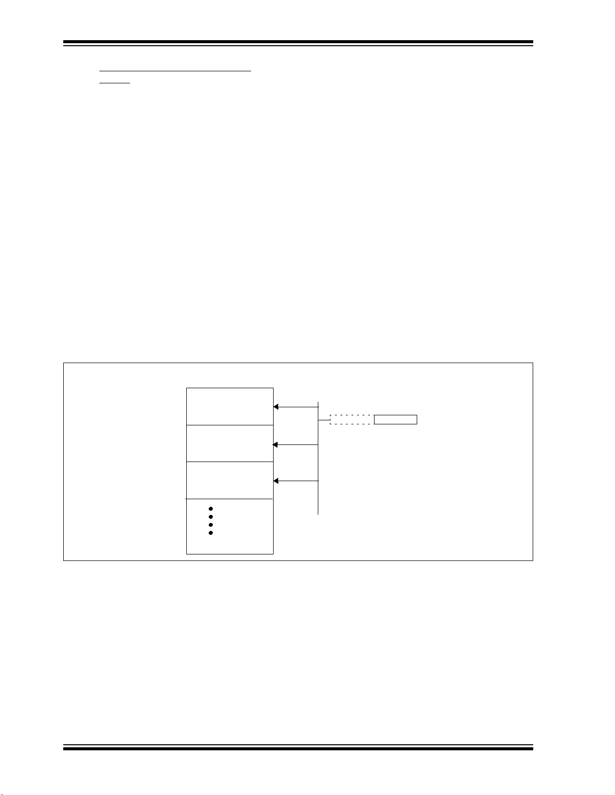
PIC18CXX2
5.2 Internal Program Memory Read/
Writes
5.2.1 TABLE READ OVERVIEW (TBLRD) The TBLRD in structions are use d to read data fr om pro-
gram memory to data memory.
TBLPTR points to a byte address in program space.
Executing TBLRD places the byte pointed to into TAB-
LAT. In addition, TBLPTR can be modified automatically for the next Table Read operation.
Table Reads from program memo ry are perf o rmed one
byte at a time. The inst ruction will load TABLA T with the
one byte from p rogr am memory point ed to b y TBLPTR.
5.2.2 INTERNAL PROGRAM MEMORY WRITE
BLOCK SIZE
The internal program memory of PIC18CXXX devices
is written in blocks. For PIC18CXX2 devices, the write
block size is 2 bytes. Consequently, Table Write operations to internal program memory are performed in
pairs, one byte at a time.
When a Table Write occurs to an even program memory address (TBLPTR<0> = 0), t he conte nts of TABLAT
are transferred to an internal holding register. This is
performed as a short write and the program memory
block is not actually p rogramm ed at this time . The holding register is not accessible by the user.
When a Table Write occurs to an odd pro gr am memo ry
address (TBLPTR,)>=1), a long write is started. During
the long write, th e contents of TABLA T are written to the
high byte of the program memory block and the contents of the holding register are transferred to the low
byte of the program memory block.
Figure 5-3 shows the holding register and the program
memory write blocks.
If a single byte is to be prog rammed, the lo w (ev en) byte
of the destination program word should be read using
TBLRD*, modified or changed, if required, and written
back to the same address using TBLWT*+. The high
(odd) byte should be read using TBLRD*, modified or
changed if required, and written back to the same
address using TBLWT. The write to an odd address will
cause a long write to begin. This process ensures that
existing data in either byte will not be changed unless
desired.
FIGURE 5-3: HOLDING REGISTER AND THE WRITE BLOCK
Program Memory (x 2-bits)
Block n
Block n + 1
Block n + 2
Write Bl ock
MSB
The write to the MSB of the Write Block
causes the en tire block to be written to pr ogram memory. The program memory block
that is written depends on the address that is
written to in the MSB of the Write Block.
Holding Register
DS39026B-page 56 Preliminary
7/99 Microchip Technology Inc.

PIC18CXX2
5.2.2.1 OPERATION The long write is what actua ll y programs words of da ta
into the internal memory. When a TBLWT to the MSB of
the write block occurs, instruction execution is halted.
During this time, programming voltage and the data
stored in internal latches is applied to program memory.
For a long write to occur:
1. MCLR
2. LWRT bit must be set
3. TBLWT to the address of the MSB of the write
If the LWRT bit is clear, a short write will occur and program memory will not be changed. If the TBLWT is not
to the MSB of the write block, then the programming
phase is not initiated.
Setting the LWRT bit enables long writes when the
MCLR
is set, it can be cleared only by performing a POR or
MCLR reset.
To ensure that the memory location has been well programmed, a minimum programming time is required.
The long write can be terminated after the programming time has expired by a reset or an interrupt. Having
only one interrupt so urce e nab led to terminate the lon g
write ensures that no unintended interrupts will prematurely terminate the long write.
/VPP pin must be at the prog ramming v olt-
age
block
pin is taken to VPP voltage. Once the LWRT bit
5.2.2.2 SEQUENCE OF EVENTS The sequence of events for programming an internal
program memory location should be:
1. Enable the interrupt that terminates the long
write. Disable all other interrupts.
2. Clear the source interrupt flag.
3. If Interrupt Service Routine execution is desired
when the device wakes, enable global interrupts.
4. Set LWRT bit in the RCON register.
5. Raise MCLR
age, V
6. Clear the WDT (if enabled).
7. Set the interrupt source to interrupt at the
required time.
8. Execute the table write for the lower (e v en) b yte.
This will be a short write.
9. Execute the table write for the upper (odd) byte.
This will be a long w rite. The controlle r will go to
sleep while programming. The interrupt wakes
the controller.
10. If GIE was set, service the interrupt request.
11. Lower MCLR
12. Verify the memory location (table read).
/VPP pin to the pr ogramming volt-
PP.
/VPP pin to VDD.
7/99 Microchip Technology Inc.
Preliminary DS39026B-page 57

PIC18CXX2
5.2.3 INTERRUPTS The long write must be terminated by a reset or any
interrupt.
The interrupt source must have its interrupt enable bit
set. When the source sets its interrupt flag, programming will ter minate. This will oc cur regardless of the
settings of interrupt priority bits , the GIE/GIEH bit or th e
PIE/GIEL bit.
Depending on the states of interrupt priority bits, the
GIE/GIEH bit or the PIE/GIEL bit, program execution
can either be vectored to the high or low priority Interrupt Service Routine (ISR) or continue execution from
where programming commenced.
In either case, the interrupt flag will not be cleared
when programming is terminated and will need to be
cleared by the software.
TABLE 5-2: SLEEP MODE, INTERRUPT ENABLE BITS AND INTERRUPT RESULTS
GIE/
GIEH
XX X 0
X X X 1 0 Long write continues, will wake when
0
(default)0(default)
0
(default)
PIE/
GIEL
11
Priority
X 1 1 Terminates long write,
high priority
(default)
Interrupt
Enable
(default)
1 1 Terminates long write,
Interrupt
Flag
X Long write continues even if interrupt
flag becomes set during sleep.
the interrupt flag is set.
executes next instruction. Interrupt flag
not cleared.
executes next instruction. Interrupt flag
not cleared.
Action
10
(default)
0
(default)
10
10
(default)1high priority
0
low
low
(default)
1 1 Terminates long write, executes next
instruction. Interrupt flag not cleared.
1 1 Terminates long write, branches to low
priority interrupt vector.
Interrupt flag can be cleared by ISR.
1 1 Terminates long write, branches to high
priority interrupt vector.
Interrupt flag can be cleared by ISR.
DS39026B-page 58 Preliminary
7/99 Microchip Technology Inc.

5.2.4 UNEXPECTED TERMINATION OF WRITE OPERATIONS
If a write is terminated by an unplanned event such as
loss of powe r, an unexpected reset, or an in terrup t th at
was not disabled, the memory location just programmed should be verified and reprogrammed if
needed.
PIC18CXX2
7/99 Microchip Technology Inc.
Preliminary DS39026B-page 59

PIC18CXX2
NOTES:
DS39026B-page 60 Preliminary
7/99 Microchip Technology Inc.

PIC18CXX2
6.0 8 X 8 HARDWARE MULTIPLIER
6.1 Introduction
An 8 x 8 hardware multiplier is included in the ALU of
the PIC18CXX2 devices. By making the multiply a
hardware oper at ion , it c om pl ete s in a single instruction
cycle. This is an unsigned multiply that gives a 16-bit
result. The result is store d into th e 16-bit produ ct regi ster pair (PRODH:PRODL). The multiplier does not
affect any flags in the ALUSTA register.
Making the 8 x 8 multiplier execute in a single cycle
gives the following advantages:
• Higher computational throughput
• Reduces code si z e req uirements for multiply algorithms
The performance i ncrease all ows the de vice to be used
in applications previously reserved for Digital Signal
Processors.
Table 6-1 shows a performance comparison between
enhanced de vices using the s ingle cycle hardw are multiply, and performing the same function without the
hardware multiply.
TABLE 6-1: PERFORMANCE COMPARISON
Routine Multiply Method Program
Memory
(Words)
8 x 8 unsigned Without hardware multiply 13 69 6.9 µs27.6 µs69 µs
Hardware multiply 1 1 100 ns 400 ns 1 µs
8 x 8 signed Without hardware multiply 33 91 9.1 µs36.4 µs91 µs
Hardware multiply 6 6 600 ns 2.4 µs6 µs
16 x 16 unsigned Without hardware multiply 21 242 24.2 µs96.8 µs242 µs
Cycles
(Max)
Time
@ 40 MHz @ 10 MHz @ 4 MHz
Hardware multiply 24 24 2.4 µs9.6 µs24 µs
16 x 16 signed Without hardware multiply 52 254 25.4 µs 102.6 µs254 µs
Hardware multiply 36 36 3.6 µs14.4 µs36 µs
7/99 Microchip Technology Inc.
Preliminary DS39026B-page 61

PIC18CXX2
6.2 Operation
Example 6-1 shows the sequence to do an 8 x 8
unsigned multiply. Only one instruction is required
when one argumen t of the multiply i s alre ady l oad ed in
the WREG register.
Example 6-2 shows th e sequence t o do an 8 x 8 s igned
multiply. To account for the sign bits of the arguments,
each argument’s most significant bit (MSb) is tested
and the appropriate subtractions are done.
EXAMPLE 6-1: 8 x 8 UNSIGNED MULTIPLY
ROUTINE
MOVFF ARG1, WREG ;
MULWF ARG2 ; ARG1 * ARG2 ->
; PRODH:PRODL
EXAMPLE 6-2: 8 x 8 SIGNED MULTIPLY
ROUTINE
MOVFF ARG1, WREG
MULWF ARG2 ; ARG1 * ARG2 ->
; PRODH:PRODL
BTFSC ARG2, SB ; Test Sign Bit
SUBWF PRODH, F ; PRODH = PRODH
; - ARG1
MOVFF ARG2, WREG
BTFSC ARG1, SB ; Test Sign Bit
SUBWF PRODH, F ; PRODH = PRODH
; - ARG2
Example 6-3 shows the sequence to do a 16 x 16
unsigned multiply. Equation 6-1 shows the algorithm
that is used. The 32-bit result is stored in 4 registers
RES3:RES0.
EQUATION 6-1: 16 x 16 UNSIGNED
MULTIPLICATION
ALGORITHM
RES3:RES0 = ARG1H:ARG1L • ARG2H:ARG2L
= (ARG1H • ARG2H • 2
(ARG1H • ARG2L • 2
(ARG1L • ARG2H • 2
(ARG1L • ARG2L)
16
)+
8
)+
8
)+
EXAMPLE 6-3: 16 x 16 UNSIGNED
MULTIPLY ROUTINE
MOVFF ARG1L, WREG
MULWF ARG2L ; ARG1L * ARG2L ->
; PRODH:PRODL
MOVFF PRODH, RES1 ;
MOVFF PRODL, RES0 ;
;
MOVFF ARG1H, WREG
MULWF ARG2H ; ARG1H * ARG2H ->
; PRODH:PRODL
MOVFF PRODH, RES3 ;
MOVFF PRODL, RES2 ;
;
MOVFF ARG1L, WREG
MULWF ARG2H ; ARG1L * ARG2H ->
; PRODH:PRODL
MOVFF PRODL, WREG ;
ADDWF RES1, F ; Add cross
MOVFF PRODH, WREG ; products
ADDWFC RES2, F ;
CLRF WREG, F ;
ADDWFC RES3, F ;
;
MOVFF ARG1H, WREG ;
MULWF ARG2L ; ARG1H * ARG2L ->
; PRODH:PRODL
MOVFF PRODL, WREG ;
ADDWF RES1, F ; Add cross
MOVFF PRODH, WREG ; products
ADDWFC RES2, F ;
CLRF WREG, F ;
ADDWFC RES3, F ;
Example 6-4 shows the sequence to do an 16 x 16
signed multiply. Equation 6-2 shows the algorithm
used. The 32-bit result is stored in four registers
RES3:RES0. To account for the sign bits of the arguments, each argument pairs most significant bit (MSb)
is tested and the appropriate subtractions are done.
EQUATION 6-2: 16 x 16 SIGNED
MULTIPLICATION
ALGORITHM
RES3:RES0
= ARG1H:ARG1L • ARG2H:ARG2L
= (ARG1H • ARG2H • 2
(ARG1H • ARG2L • 2
(ARG1L • ARG2H • 2
(ARG1L • ARG2L)+
(-1 • ARG2H<7> • ARG1H:ARG1L • 2
(-1 • ARG1H<7> • ARG2H:ARG2L • 2
16
)+
8
)+
8
)+
16
)+
16
)
DS39026B-page 62 Preliminary
7/99 Microchip Technology Inc.

EXAMPLE 6-4: 16 x 16 SIGNED MULTIPLY
ROUTINE
MOVFF ARG1L, WREG
MULWF ARG2L ; ARG1L * ARG2L ->
; PRODH:PRODL
MOVFF PRODH, RES1 ;
MOVFF PRODL, RES0 ;
;
MOVFF ARG1H, WREG
MULWF ARG2H ; ARG1H * ARG2H ->
; PRODH:PRODL
MOVFF PRODH, RES3 ;
MOVFF PRODL, RES2 ;
;
MOVFF ARG1L, WREG
MULWF ARG2H ; ARG1L * ARG2H ->
; PRODH:PRODL
MOVFF PRODL, WREG ;
ADDWF RES1, F ; Add cross
MOVFF PRODH, WREG ; products
ADDWFC RES2, F ;
CLRF WREG, F ;
ADDWFC RES3, F ;
;
MOVFF ARG1H, WREG ;
MULWF ARG2L ; ARG1H * ARG2L ->
; PRODH:PRODL
MOVFF PRODL, WREG ;
ADDWF RES1, F ; Add cross
MOVFF PRODH, WREG ; products
ADDWFC RES2, F ;
CLRF WREG, F ;
ADDWFC RES3, F ;
;
BTFSS ARG2H, 7 ; ARG2H:ARG2L neg?
GOTO SIGN_ARG1 ; no, check ARG1
MOVFF ARG1L, WREG ;
SUBWF RES2 ;
MOVFF ARG1H, WREG ;
SUBWFB RES3
;
SIGN_ARG1
BTFSS ARG1H, 7 ; ARG1H:ARG1L neg?
GOTO CONT_CODE ; no, done
MOVFF ARG2L, WREG ;
SUBWF RES2 ;
MOVFF ARG2H, WREG ;
SUBWFB RES3
;
CONT_CODE
:
PIC18CXX2
7/99 Microchip Technology Inc.
Preliminary DS39026B-page 63

PIC18CXX2
NOTES:
DS39026B-page 64 Preliminary
7/99 Microchip Technology Inc.

PIC18CXX2
7.0 INTERRUPTS
The PIC18CXX2 devices have multiple interrupt
sources and an interrupt priority feature that allows
each interrupt source to be assigned a high priority
level or a low priority level. The high priority interrupt
vector is at 0000 08h and the low priority interrupt vector
is at 000018h. High priority interrupt events will override any low priority interrupts that may be in progress.
There are ten registers which are used to control interrupt operation. These registers are:
• RCON
•INTCON
• INTCON2
• INTCON3
• PIR1, PIR2
• PIE1, PIE2
• IPR1, IPR2
It is recommended that the Microchip header files supplied with MPLAB be used for the symbolic bit names
in these registers. This allows the assembler/compiler
to automatically tak e care of the placement of these bit s
within the specified register.
Each interrupt source has three bits to control its operation. The functions of these bits are:
• Flag bit to indicate that an interrupt event
occurred
• Enable bit that allows pr ogram execution to
branch to the interrupt ve ctor address when
the flag bit is set
• Priority bit to select high priority or lo w priority
The interr upt pri ority featu re is enabled by setting the
IPEN bit (RCON<7>). When interrupt priority is
enabled, the re are tw o bits wh ich e nab le in terrupts globally. Setting the GIEH bit (INTCON<7>) enables all
interrupts that hav e the priority bit set. Setting the GIEL
bit (INTCON<6>) enables all interrupts that have the
priority bit cleared. When the interrupt flag, enable bit
and appropriate global interrupt enable it are set, the
interrupt will v ecto r imme diatel y to a ddress 00000 8h or
000018h depending on the priority level. Individual
interrupts can be disabled through their corresponding
enable bits.
When the IPEN bit is cleared (default state), the interrupt priority feature is disabled and interrupts are compatible with PICmicro mid-range devices. In
compatibility mode, the interrupt priority bits for each
source have no effect. INTCON<6> is the PEIE bit,
which enable s/disab les all peripher al inte rrupt sources .
INTCON<7> is the GIE bit, which enables/disables all
interrupt sources. All interrupts branch to address
000008h in compatibility mode.
When an interrupt is res po nde d to, the Global Interrupt
Enable bit is c le ared t o dis able further interrupts. If th e
IPEN bit is cleared, this is the GIE bit. If interrupt priority levels are used, this will be either the GIEH or GIEL
bit. High priority interrupt sources can interrupt a low
priority interrupt.
The return address is pushed onto the stack and the
PC is loaded with the interrupt vector address
(000008h or 000018h). Once in the interrupt service
routine, the source(s) of the interrupt can be determined by polling the interrupt flag bits. The interrupt
flag bits must b e cle ared i n sof tware bef ore re-ena b ling
interrupts to avoid recursive interrupts.
The "return from interrupt" instruction, RETFIE, exits
the interrupt routine and se ts the GIE bit (GI EH or GIEL
if priority levels are used), which re-enables interrupts.
For external interrupt events, such as the INT pins or
the PORTB input c hange interrupt, th e interrupt latency
will be three to four instruction cycles. The exact
latency is the same for one or two cycle instr uctions.
Individual interrupt flag bits are set regardless of the
status of their corresponding enable bit or the GIE bit.
7/99 Microchip Technology Inc.
Preliminary DS39026B-page 65

PIC18CXX2
FIGURE 7-1: INTE RRUPT LOGIC
Peripheral Interrupt Flag bit
Peripheral Interrupt Enable bit
Peripheral Interrupt Priority bit
TMR1IF
TMR1IE
TMR1IP
XXXXIF
XXXXIE
XXXXIP
High Priority Interrupt Generation
Low Priority Interrupt Generation
Peripheral Interrupt Flag bit
Peripheral Interrupt Enable bit
Peripheral Interrupt Priority bit
TMR1IF
TMR1IE
TMR1IP
XXXXIF
XXXXIE
XXXXIP
Additional Peripheral Interrupts
Additional Peripheral Interrupts
T0IF
T0IE
T0IP
RBIF
RBIE
RBIP
INT0F
INT0E
INT1F
INT1E
INT1P
INT2F
INT2E
INT2P
IPE
IPE
GIEL/PEIE
T0IF
T0IE
T0IP
RBIF
RBIE
RBIP
INT0F
INT0E
INT1F
INT1E
INT1P
INT2F
INT2E
INT2P
IPE
Wake-up if in SLEEP mode
Interrupt to CPU
Vector to location
0008h
GIEH/GIE
Interrupt to CPU
Vector to Location
0018h
GIEL\PEIE
DS39026B-page 66 Preliminary
7/99 Microchip Technology Inc.

7.0.1 INTCON REGISTERS The INTCON Registers are readable and writable
registers, which contains various enable, priority and
flag bits.
Register 7-1: INTCON Register
R/W-0 R/W-0 R/W-0 R/W-0 R/W-0 R/W-0 R/W-0 R/W-x
GIE/GIEH PEIE/GIEL TMR0IE INT0IE R BIE TMR0IF INT0IF RBIF
bit 7 bit 0
bit 7 GIE/GIEH: Global Interrupt Enable bit
When
IPEN = 0:
1 = Enables all un-masked interrupts
0 = Disables all interrupts
When IPEN = 1:
1 = Enables all interrupts
0 = Disables all interrupts
bit 6 PEIE/GEIL: Peripheral Interrupt Enable bit
IPEN = 0:
When
1 = Enables all un-masked peripheral interrupts
0 = Disables all peripheral interrupts
When IPEN = 1:
1 = Enables all low priority peripheral interrupts
0 = Disables all priority peripheral interrupts
bit 5 TMR0IE: TMR0 Overflow Interrupt Enable bit
1 = Enables the TMR0 overflow interrupt
0 = Disables the TMR0 overflow interrupt
bit 4 INT0IE: INT0 External Interrupt Enable bit
1 = Enables the INT0 external interrupt
0 = Disables the INT0 external interrupt
bit 3 RBIE: RB Port Change Interrupt Enable bit
1 = Enables the RB port change interrupt
0 = Disables the RB port change interrupt
bit 2 TMR0IF: TMR0 Overflow Interrupt Flag bit
1 = TMR0 register has overflowed (must be cleared in software)
0 = TMR0 register did not overflow
bit 1 INT0IF: INT0 External Interrupt Flag bit
1 = The INT0 external interrupt occurred (must be cleared in software)
0 = The INT0 external interrupt did not occur
bit 0 RBIF: RB Port Change Interrupt Flag bit
1 = At least one of the RB7:RB4 pins changed state (must be cleared in software)
0 = None of the RB7:RB4 pins have changed state
PIC18CXX2
Legend:
R = Readable bit W = Writable bit U = Unimplemented bit, read as ‘0’
- n = Value at POR reset ’1’ = Bit is set ’0’ = Bit is cleared x = Bit is unknown
Note: Interrupt flag bits get set when an interrupt condition occurs, regardless of the state
of its corresponding e nable bit or the glob al enable bit. User s oftware should ensure
the appropriate interrupt fl ag bi ts are clear prior to e nab ling an in terrupt. This feature
allows for software polling.
7/99 Microchip Technology Inc.
Preliminary DS39026B-page 67

PIC18CXX2
Register 7-2: INTCON2 Register
R/W-1 R/W-1 R/W-1 R/W-1 U-0 R/W-1 U-0 R/W-1
RBPU
bit 7 bit 0
bit 7 RBPU: PORTB Pull-up Enable bit
1 = All PORTB pull-ups are disabled
0 = PORTB pull-ups are enabled by individual port latch values
bit 6 INTEDG0:External Interrupt0 Edge Select bit
1 = Interrupt on rising edge
0 = Interrupt on falling edge
bit 5 INTEDG1: External Interrupt1 Edge Select bit
1 = Interrupt on rising edge
0 = Interrupt on falling edge
bit 4 INTEDG2: External Interrupt2 Edge Select bit
1 = Interrupt on rising edge
0 = Interrupt on falling edge
bit 3 Unimplemented: Read as '0'
bit 2 TMR0IP: TMR0 Overflow Interrupt Priority bit
1 = High priority
0 = Low priority
bit 1 Unimplemented: Read as '0'
bit 0 RBIP: RB Port Change Interrupt Priority bit
1 = High priority
0 = Low priority
INTEDG0 INTEDG1 INTEDG2
—
TMR0IP
—
RBIP
Legend:
R = Readable bit W = Writable bit U = Unimplemented bit, read as ‘0’
- n = Value at POR reset ’1’ = Bit is set ’0’ = Bit is cleared x = Bit is unknown
Note: Interrupt flag bits get set when an interrupt condition occurs, regardless of the state
of its corresponding e nable bit or the glob al enable bit. User s oftware should ensure
the appropriate interrupt f lag bi ts are clear prior t o enab l ing an interrupt. This feature
allows for software polling.
DS39026B-page 68 Preliminary
7/99 Microchip Technology Inc.

Register 7-3: INTCON3 Register
R/W-1 R/W-1 U-0 R/W-0 R/W-0 U-0 R/W-0 R/W-0
PIC18CXX2
INT2IP INT1IP
bit 7 bit 0
bit 7 INT2IP: INT2 External Interrupt Priority bit
1 =High priority
0 =Low priority
bit 6 INT1IP: INT1 External Interrupt Priority bit
1 =High priority
0 =Low priority
bit 5 Unimplemented: Read as '0'
bit 4 INT2IE: INT2 External Interrupt Enable bit
1 =Enables the INT2 external interrupt
0 =Disables the INT2 external interrupt
bit 3 INT1IE: INT1 External Interrupt Enable bit
1 =Enables the INT1 external interrupt
0 =Disables the INT1 external interrupt
bit 2 Unimplemented: Read as '0'
bit 1 INT2IF: INT2 External Interrupt Flag bit
1 =The INT2 external interrupt occurred
(must be cleared in software)
0 =The INT2 external interrupt did not occur
bit 0 INT1IF: INT1 External Interrupt Flag bit
1 =The INT1 external interrupt occurred
(must be cleared in software)
0 =The INT1 external interrupt did not occur
—
INT2IE INT1IE
—
INT2IF INT1IF
Legend:
R = Readable bit W = Writable bit U = Unimplemented bit, read as ‘0’
- n = Value at POR reset ’1’ = Bit is set ’0’ = Bit is cleared x = Bit is unknown
Note: Interrupt flag bits get set when an interrupt condition occurs, regardless of the state
of its corresponding e nable bit or the glob al enable bit. User s oftware should ensure
the appropriate interrupt fl ag bi ts are clear prior to e nab ling an in terrupt. This feature
allows for software polling.
7/99 Microchip Technology Inc.
Preliminary DS39026B-page 69

PIC18CXX2
7.0.2 PIR REGISTERS The PIR registers contain th e individu al flag bi ts f o r the
peripheral interrupts. Due to he number of peripheral
interrupt sources, there are two Peripheral Interrupt
Flag Registers (PIR1, PIR2).
Note 1: Interrupt flag bits get set when an interrupt
condition occurs , regardless of the state of
its corresponding enable bit or the global
enable bit, GIE (INTCON<7>).
Note 2: User softw ar e should e nsure th e approp ri-
ate interrupt flag bits are cleared prior to
enabling an interrupt, and after servicing
that interrupt.
Register 7-4: RCON Register
R/W-0 R/W-0 U-0 R/W-1 R/W-1 R/W-1 R/W-0 R/W-0
IPEN LWRT
—RITO PD POR BOR
7.0.3 PIE REGISTERS The PIE registers contain the individual enable bits for
the peripheral interrupts. Due to the number of peripheral interrupt sources, there are two Per ipheral Interrupt Enable Registers (PIE1, PIE2). When IPEN = 0,
the PEIE bit must be s et to e na b l e an y o f th es e p eripheral interrupts.
7.0.4 IPR REGISTERS The IPR registers contain the individual priority bits for
the peripheral interrupts. Due to on the number of
peripheral interrupt sources, there are two Peripheral
Interrupt Priority Registers (IPR1, IPR2). The opera tion
of the priority bits requires that the Interrupt Priority
Enable (IPEN) bit be set.
7.0.5 RCON REGISTER
The RCON register contains the bit which is used to
enable prioritized interrupts (IPEN).
bit 7 bit 0
bit 7 IPEN: Interrupt Priority Enable bit
1 = Enable priority levels on interrupts
0 = Disable priority levels on interrupts (16CXXX compatibility mode)
bit 6 LWRT: Long Write Enable
For details of bit operation see Register 4-1
bit 5 Unimplemented: Read as ’0’
bit 4 RI
bit 3 TO
bit 2 PD
bit 1 POR
bit 0 BOR
: Reset Instru ction Flag bit
For details of bit operation see Register 4-1
: Watchdog Time-out Flag bit
For details of bit operation see Register 4-1
: Power-down Detection Flag bit
For details of bit operation see Register 4-1
: Power-on Reset Status bit
For details of bit operation see Register 4-1
: Brown-out Reset Status bit
For details of bit operation see Register 4-1
Legend:
R = Readable bit W = Writable bit U = Unimplemented bit, read as ‘0’
- n = Value at POR reset ’1’ = Bit is set ’0’ = Bit is cleared x = Bit is unknown
DS39026B-page 70 Preliminary
7/99 Microchip Technology Inc.

PIC18CXX2
Register 7-5: Peripheral Interrupt Request (Flag) Registers
R/W-0 R/W-0 R-0 R-0 R/W-0 R/W-0 R/W-0 R/W-0
PIR1 PSPIF ADIF RCIF TXIF SSPIF CCP1IF TMR2IF TMR1IF
bit 7 bit 0
U-0 U-0 U-0 U-0 R/W-0 R/W-0 R/W-0 R/W-0
PIR2 — — — — BCLIF LVDIF TMR3IF CCP2IF
bit 7 bit 0
PIR1 bit 7 PSPIF: Parallel Slave Port Read/Write Interrupt Flag bit
1 = A read or a write operation has taken place
(must be cleared in software)
0 = No read or write has occurred
bit 6 ADIF: A/D Converter Interrupt Flag bit
1 = An A/D conversion completed
(must be cleared in software)
0 = The A/D conversion is not complete
bit 5 RCIF: USART Receive Interrupt Flag bit
1 = The USART receive buffer, RCREG, is full
(cleared when RCREG is read)
0 = The USART receive buffer is empty
bit 4 TXIF: USART Transmit Interrupt Flag bit
1 = The USART transmit buffer, TXREG, is empty
(cleared when TXREG is written)
0 = The USART transmit buffer is full
bit 3 SSPIF: Master Synchronous Serial Port Interrupt Flag bit
1 = The transmission/reception is complete
(must be cleared in software)
0 = Waiting to transmit/receive
bit 2 CCP1IF: CCP1 Interrupt Flag bit
Capture Mode
1 = A TMR1 register capture occurred
(must be cleared in software)
0 = No TMR1 register capture occurred
Compare Mode
1 = A TMR1 register compare match occurred
(must be cleared in software)
0 = No TMR1 register compare match occurred
PWM Mode
Unused in this mode
bit 1 TMR2IF: TMR2 to PR2 Match Interrupt Flag bit
1 = TMR2 to PR2 match occurred
(must be cleared in software)
0 = No TMR2 to PR2 match occurred
bit 0 TMR1IF: TMR1 Overflow Interrupt Flag bit
1 = TMR1 register overflowed
(must be cleared in software)
0 = TMR1 register did not overflow
7/99 Microchip Technology Inc.
Preliminary DS39026B-page 71

PIC18CXX2
Register 7-5: Peripheral Interrupt Request (Flag) Registers (cont’d)
PIR2 bit 7-4 Unimplemented: Read as ’0’
bit 3 BCLIF: Bus Collision Interrupt Flag bit
1 = A Bus Collision occurred
(must be cleared in software)
0 = No Bus Collision occurred
bit 2 LVDIF: Low-Voltage Detect Interrupt Flag bit
1 = A low voltage condition occurred
(must be cleared in software)
0 = The device voltage is above the Low Voltage Detect trip point
bit 1 TMR3IF: TMR3 Overflow Interrupt Flag bit
1 = TMR3 register overflowed
(must be cleared in software)
0 = TMR3 register did not overflow
bit 0 CCP2IF: CCPx Interrupt Flag bit
Capture Mode
1 = A TMR1 register capture occurred
(must be cleared in software)
0 = No TMR1 register capture occurred
Compare Mode
1 = A TMR1 register compare match occurred
(must be cleared in software)
0 = No TMR1 register compare match occurred
PWM Mode
Unused in this mode
Legend:
R = Readable bit W = Writable bit U = Unimplemented bit, read as ‘0’
- n = Value at POR reset ’1’ = Bit is set ’0’ = Bit is cleared x = Bit is unknown
DS39026B-page 72 Preliminary
7/99 Microchip Technology Inc.

PIC18CXX2
Register 7-6: Peripheral Interrupt Enable Registers
R/W-0 R/W-0 R/W-0 R/W-0 R/W-0 R/W-0 R/W-0 R/W-0
PIE1
bit 7 bit 0
PIE2
PIE1 bit 7 PSPIE: Parallel Slave Port Read/Write Interrupt Enable bit
PSPIE ADIE RCIE TXIE SSPIE CCP1IE TMR2IE TMR1IE
U-0 U-0 U-0 U-0 R/W-0 R/W-0 R/W-0 R/W-0
— — — — BCLIE LVDIE TMR3IE CCP2IE
bit 7 bit 0
1 = Enables the PSP read/write interrupt
0 = Disables the PSP read/write interrupt
bit 6 ADIE: A/D Converter Interrupt Enable bit
1 = Enables the A/D interrupt
0 = Disables the A/D interrupt
bit 5 RCIE: USART Receive Interrupt Enable bit
1 = Enables the USART receive interrupt
0 = Disables the USART receive interrupt
bit 4 TXIE: USART Transmit Interrupt Enable bit
1 = Enables the USART transmit interrupt
0 = Disables the USART transmit interrupt
bit 3 SSPIE: Master Synchronous Serial Port Interrupt Enable bit
1 = Enables the MSSP interrupt
0 = Disables the MSSP interrupt
bit 2 CCP1IE: CCP1 Interrupt Enable bit
1 = Enables the CCP1 interrupt
0 = Disables the CCP1 interrupt
bit 1 TMR2IE: TMR2 to PR2 Match Interrupt Enable bit
1 = Enables the TMR2 to PR2 match interrupt
0 = Disables the TMR2 to PR2 match interrupt
bit 0 TMR1IE: TMR1 Overflow Interrupt Enable bit
1 = Enables the TMR1 overflow interrupt
0 = Disables the TMR1 overflow interrupt
PIE2 bit 7-4 Unimplemented: Read as '0'
bit 3 BCLIE: Bus Collision Interrupt Enable bit
1 = Enabled
0 = Disabled
bit 2 LVDIE: Low-voltage Detect Interrupt Enable bit
1 = Enabled
0 = Disabled
bit 1 TMR3IE: TMR3 Overflow Interrupt Enable bit
1 = Enables the TMR3 overflow interrupt
0 = Disables the TMR3 overflow interrupt
bit 0 CCP2IE: CCP2 Interrupt Enable bit
1 = Enables the CCP2 interrupt
0 = Disables the CCP2 interrupt
Legend:
R = Readable bit W = Writable bit U = Unimplemented bit, read as ‘0’
- n = Value at POR reset ’1’ = Bit is set ’0’ = Bit is cleared x = Bit is unknown
7/99 Microchip Technology Inc.
Preliminary DS39026B-page 73

PIC18CXX2
Register 7-7: Peripheral Interrupt Priority Registers
R/W-1 R/W-1 R/W-1 R/W-1 R/W-1 R/W-1 R/W-1 R/W-1
IPR1 PSPIP ADIP RCIP TXIP SSPIP CCP1IP TMR2IP TMR1IP
bit 7 bit 0
U-0 U-0 U-0 U-0 R/W-1 R/W-1 R/W-1 R/W-1
IPR2 — — — — BCLIP LVDIP TMR3IP CCP2IP
bit 7 bit 0
IPR1 bit 7 PSPIP: Parallel Slave Port Read/Write Interrupt Priority bit
1 = High priority
0 = Low priority
bit 6 ADIP: A/D Converter Interrupt Priority bit
1 = High priority
0 = Low priority
bit 5 RCIP: USART Receive Interrupt Priority bit
1 = High priority
0 = Low priority
bit 4 TXIP: USART Transmit Interrupt Priority bit
1 = High priority
0 = Low priority
bit 3 SSPIP: Master Synchronous Serial Port Interrupt Priority bit
1 = High priority
0 = Low priority
bit 2 CCP1IP: CCP1 Interrupt Priority bit
1 = High priority
0 = Low priority
bit 1 TMR2IP: TMR2 to PR2 Match Interrupt Priority bit
1 = High priority
0 = Low priority
bit 0 TMR1IP: TMR1 Overflow Interrupt Priority bit
1 = High priority
0 = Low priority
IPR2 bit 7-4 Unimplemented: Read as '0'
bit 3 BCLIP: Bus Collision Interrupt Priority bit
1 = High priority
0 = Low priority
bit 2 LVDIP: Low-voltage Detect Interrupt Priority bit
1 = High priority
0 = Low priority
bit 1 TMR3IP: TMR3 Overflow Interrupt Priority bit
1 = High priority
0 = Low priority
bit 0 CCP2IP: CCP2 Interrupt Priority bit
1 = High priority
0 = Low priority
Legend:
R = Readable bit W = Writable bit U = Unimplemented bit, read as ‘0’
- n = Value at POR reset ’1’ = Bit is set ’0’ = Bit is cleared x = Bit is unknown
DS39026B-page 74 Preliminary
7/99 Microchip Technology Inc.

PIC18CXX2
7.0.6 INT0 INTERRUPT External interrupts on the RB0/INT0, RB1/INT1 and
RB2/INT2 pins are edge triggered: either rising if the
corresponding INTEDGx b it is set in the INTCON2 re gister, or falling, if the INTEDGx bit is clear. When a valid
edge appears on the RBx/INTx pin, the corresponding
flag bit INTxF is set. This interrupt can be disabled by
clearing the cor respondi ng enable bit INT xE. Fla g bit
INTxF must be cleared in software in the interrupt service routine before re-enabling the interrupt. All external interrupts (INT0, INT1 and INT2) can wake-up the
processor from SLEEP, if bit INTxE was set prior to
going into SLEEP. If the global in terrupt enable bit G IE
set, the processor will br anch to the inter rupt v ecto r f ollowing wake-up.
Interrupt priority for INT1 and INT2 is determined b y the
value contained in the interrupt priority bits INT1IP
(INTCON3<6>) and INT2IP (INTCON3<7>). There is
no priority bit associated with INT0. It is always a high
priority interrupt source.
7.0.7 TMR0 INTERRUPT In 8-bit mode (which is the d efa ult), an ov erflo w (FFh →
00h) in the TMR0 register will set flag bit TMR0IF. In
16-bit mode, an overflow (FFFFh → 0000h) in the
TMR0H:TMR0L registers will set flag bit TMR0IF. The
interrupt can be enabled/disabled by setting/clearing
enable bit T0IE (INTCON<5>). Interrupt priority for
Timer0 is determined by the value contained in the
interrupt priority bit TMR0IP (INTCON2<2>). See Section 8.0 for further details on the Timer0 module.
7.0.8 PORTB INTERRUPT ON CHANGE An input change on PORTB<7:4> sets flag bit RBIF
(INTCON<0>). The interrupt can be enabled/disabled
by setting/clearing enable bit RBIE (INTCON<3>).
Interrupt priority for PORTB Interrupt on change is
determined by the value contained in the interrupt priority bit RBIP (INTCON2<0>).
7.1 Context Saving During Inte rr upts
During an interrupt, the return PC v alue i s sa ve d on the
stack. Additionally, the WREG, STATUS and BSR registers are sav ed on the f ast return stac k. If a f ast return
from interrupt is not used (See Section 4.3), the user
may need t o s ave the WR EG, STATUS a nd BSR regis-
ters in software. Depending on the user’s application,
other registers ma y also nee d to be sav ed. Example 61 saves and restores the WREG, STATUS and BSR
registers during an i nterrupt service routine.
EXAMPLE 7-1: SAVING STATUS, WREG AND BSR REGISTERS IN RAM
MOVWF W_TEMP ; W_TEMP is in virtual bank
MOVFF STATUS, STATUS_TEMP ; STATUS_TEMP located anywhere
MOVFF BSR, BSR_TEMP ; BSR located anywhere
;
; USER ISR CODE
;
MOVFF BSR_TEMP, BSR ; Restore BSR
MOVF W_TEMP, W ; Restore WREG
MOVFF STATUS_TEMP, STATUS ; Restore STATUS
7/99 Microchip Technology Inc.
Preliminary DS39026B-page 75

PIC18CXX2
NOTES:
DS39026B-page 76 Preliminary
7/99 Microchip Technology Inc.

PIC18CXX2
8.0 I/O PORTS
Depending on the de vic e selec ted, there are either five
ports or three ports available. Some pins of the I/O
ports are multiplexed with an alternate function from
the peripheral features on the device. In general, when
a peripheral is enabled, that pin may not be used as a
general purpose I/ O pin.
Each port has three registers for its operation. These
registers are:
• TRIS register (Data Direction register)
• PORT registe r (rea ds the levels on th e pi ns of th e
device)
• LAT register (output latch)
The data latch (LAT register) is useful for read-modifywrite operations on the value that the I/O pins are driving.
8.1 PORTA, TRISA and LATA Registers
PORTA is a 6-bit wide bi-directional port. The corresponding data direction register is TRISA. Setting a
TRISA bit (=1) will m ake the correspondi ng PORTA pin
an input, (i.e., put the corresponding output driver in a
hi-impedance mode). Clearing a TRISA bit (=0) will
make the corre sponding POR TA pin an output, (i .e., put
the contents of the output latch on the selected pin).
Note: On a Power-on Reset, these pins are con-
figured as inputs and read as '0'.
Reading the PORTA register reads the status of the
pins, whereas writing to it will write to the port latch.
The Data Latch register (LATA) is also memory
mapped. Read-modify-write operations on the LATA
register reads and writes the latched output value for
PORTA.
The RA4 pin is multiplexed with the Timer0 module
clock input to become the RA4/T0CKI pin. The RA4/
T0CKI pin is a Schmitt Trigger input and an open drain
output. All other RA p ort pins hav e TTL input le v els and
full CMOS output drivers.
The other PORTA pins are multiplexed with analog
inputs and the analog V
operation of each pin is se lected by clea ring/settin g the
control bits in the ADCON1 register (A/D Control
Register1).
Note: On a Power-on Reset, these pins are con-
figured as analog inputs and read as '0'.
The TRISA register controls the direction of the RA
pins, even when they are being used as analog inputs.
The user must ensure the bi ts in the TRISA registe r are
maintained set when using them as analog inputs.
REF+ and VREF- inputs. The
EXAMPLE 8-1: INITIALIZING PORTA
CLRF PORTA ; Initialize PORTA by
; clearing output
CLRF LATA ; Alternate method
MOVLW 0x07 ; Configure A/D
MOVWF ADCON1 ; for digital inputs
MOVLW 0xCF
MOVWF TRISA ; Set RA<3:0> as inputs
; data latches
; to clear output
; data latches
Value used to
;
; initialize data
; direction
; RA<5:4> as outputs
7/99 Microchip Technology Inc.
Preliminary DS39026B-page 77
PIC18CXX2
FIGURE 8-1: BLOCK DIAGRAM OF
RA3:RA0 AND RA5 PINS
RD LATA
Data
Bus
WR LATA
or
PORTA
WR TRISA
RD PORTA
Q
CK
Data Latch
Q
CK
TRIS Latch
QD
QD
RD TRISA
QD
Analog
input
mode
EN
VDD
P
N
V
SS
I/O pin
TTL
input
buffer
FIGURE 8-3: BLOCK DIAGRAM OF RA6
ECRA6 or
RCRA6 enable
Data
Bus
RD LATA
QD
WR LATA
or
(1)
PORTA
WR
TRISA
CK
Data Latch
CK
TRIS Latch
Q
QD
Q
ECRA6 or
RCRA6
enable
Data Bus
RD TRISA
Data Bus
VDD
P
N
SS
V
QD
I/O pin
TTL
input
buffer
(1)
SS input (RA5 only)
To A/D Converter and LVD Modules
Note 1: I/O pins have protection diodes to VDD and VSS.
FIGURE 8-2: BLOCK DIAGRAM OF RA4/
T0CKI PIN
Data
Bus
WR LATA
or
PORTA
WR TRISA
RD LATA
QD
Q
CK
Data Latch
QD
Q
CK
TRIS Latch
RD TRISA
N
SS
V
Schmitt
Trigger
input
buffer
QD
I/O pin
EN
RD PORTA
Note 1: I/O pins have protection diodes to VDD and VSS.
(1)
EN
EN
RD PORTA
TMR0 Cock Input
Note 1: I/O pin has protection diodes to VSS only.
DS39026B-page 78 Preliminary
7/99 Microchip Technology Inc.
TABLE 8-1: PORTA FUNCTIONS
Name Bit# Buffer Function
RA0/AN0 bit0 TTL Input/output or analog input
RA1/AN1 bit1 TTL Input/output or analog input
PIC18CXX2
RA2/AN2/V
RA3/AN3/VREF+ bit3 TTL Input/output or analog input or VREF+
RA4/T0CKI bit4 ST Input/output or external clock input for Timer0
RA5/SS/
OSC2/CLKO/RA6 bit6 OSC2 or clock output or I/O pin
Legend: TTL = TTL input, ST = Schmitt Trigger input
TABLE 8-2: SUMMARY OF REGISTERS ASSOCIATED WITH PORTA
Name Bit 7 Bit 6 Bit 5 Bit 4 Bit 3 Bit 2 Bit 1 Bit 0
PORT A — RA6 RA5 RA4 RA3 RA2 RA1 RA0 --0x 0000 --0u 0000
LATA
TRISA
ADCON1 ADFM ADCS2
Legend: x = unknown, u = un chang ed, - = u nimpl emen ted loc ations re ad a s ’ 0’ . Shad ed ce lls are not used b y PORTA.
REF- bit2 TTL Input/output or analog input or VREF-
Output is open drain type
AN4/LVDIN bit5 TTL Input/output or slave select input for synchronous serial port or analog
input, or low voltage detect input
Value on
POR,
BOR
— Latch A Data Output Register --xx xxxx --uu uuuu
— PORTA Data Direction Register --11 1111 --11 1111
— — PCFG3 PCFG2 PCFG1 PCFG0 --0- 0000 --0- 0000
Value on all
other
resets
7/99 Microchip Technology Inc.
Preliminary DS39026B-page 79
PIC18CXX2
8.2 PORTB, TRISB and LATB Registers
PORTB is an 8-bit wide bi-directional port. The corresponding data direction register is TRISB. Setting a
TRISB bit (=1) will mak e the correspon ding POR TB pin
an input, (i.e., put the corresponding output driver in a
hi-impedance mode). Clearing a TRISB bit (=0) will
make the corresponding PORTB pin an output, ( i.e. put
the contents of the output latch on the selected pin).
The Data Latch register (LATB) is also memory
mapped. Read-modify-write operations on the LATB
register reads and writes the latched output value for
PORTB.
EXAMPLE 8-2: INITIALIZING PORTB
CLRF PORTB ; Initialize PORTB by
CLRF LATB ; Alternate method
MOVLW 0xCF ; Value used to
MOVWF TRISB ; Set RB<3:0> as inputs
Each of the PORTB pins has a weak internal pull-up. A
single control bit ca n turn on all the pull-ups . This is performed by clearing bit RBPU
weak pull-up i s autom atically tur ned off when the po rt
pin is configured as an output. The pull-ups are disabled on a Power-on Reset.
Four of PORTB’s pins, RB7:RB4, have an interrupt on
change feature. Only pins configured as inputs can
cause this interrupt to oc cur (i.e . any RB7:RB4 pin configured as an output is excluded from the interrupt on
change comparison). The input pins (of RB7:RB4) are
compared with th e o ld value latche d o n the la st read of
PORTB. The “mismatch” outputs of RB7:RB4 are
OR’ed together to generate the RB Port Change Interrupt with flag bit RBIF (INTCON<0>).
This interrupt can wake the device from SLEEP. The
user, i n the interrupt service routine , can clear the interrupt in the following manner:
a) Any read or write of PORTB (except with the
MOVFF instruction). This will end the mismatch
condition.
b) Clear flag bit RBIF.
A mismatch condition will continue to set flag bit RBIF.
Reading PORTB will end the mismatch condition and
allow flag bit RBIF to be cleared.
The interrupt on change feature is recommended for
wake-up on key depression operation and operations
where PORTB is only used for the interrupt on change
feature. Polling of PORTB is not recommended while
using the interrupt on change feature.
; clearing output
; data latches
; to clear output
; data latches
; initialize data
; direction
; RB<5:4> as outputs
; RB<7:6> as inputs
(INTCON2<7>). The
FIGURE 8-4: BLOCK DIAGRAM OF
RB7:RB4 PINS
TTL
Input
Buffer
EN
EN
DD and VSS.
V
RD PORTB
(2)
RBPU
Data Bus
WR LATB
or
PORTB
WR TRISB
Set RBIF
From other
RB7:RB4 pins
RBx/INTx
Note 1: I/O pins have diode protection to V
2: To enable weak pull-ups, set the appropriate TRIS
Data Latch
QD
CK
TRIS Latch
QD
CK
RD TRISB
RD LATB
RD PORTB
bit(s) and clear the RBPU
Latch
QD
QD
bit (INTCON2<7>).
FIGURE 8-5: BLOCK DIAGRAM OF
RB2:RB0 PINS
(2)
RBPU
Data Bus
WR Port
WR TRIS
RB0/INT
Note 1: I/O pins have diode protection to V
2: To enable weak pull-ups, set the appropriate TRIS
bit(s) and clear the RBPU
Data Latch
CK
TRIS Latch
CK
RD TRIS
RD Port
Schmitt Trigger
Buffer
QD
QD
QD
EN
DD and VSS.
bit (OPTION_REG<7>).
TTL
Input
Buffer
DD
P
weak
pull-up
I/O
pin
Buffer
Q1
V
DD
weak
P
pull-up
RD Port
Q3
(1)
ST
I/O
pin
(1)
DS39026B-page 80 Preliminary
7/99 Microchip Technology Inc.

FIGURE 8-6: BLOCK DIAGRAM OF RB3
(2)
RBPU
CCP2MX
CCP Output
(3)
(3)
Enable
CCP Output
Data Bus
WR LATB or
WR PORTB
WR TRISB
1
Data Latch
QD
CK
TRIS Latch
D
CK
Q
RD TRISB
RD LATB
0
Q
PIC18CXX2
V
DD
weak
P
pull-up
V
DD
P
I/O
(1)
N
VSS
TTL
Input
Buffer
D
Pin
RD PORTB
RD PORTB
CCP2 input
Note 1: I/O pin has diode protection to VDD and VSS.
2: To enable weak pull-ups, set the appropriate DDR bit(s) and clear the RBPU
3: The CCP2 input/output is multiplexed with RB3 if the CCP2MX bit is enabled (=’0’) in the configuration register.
(3)
Schmitt Trigger
Buffer
CCP2MX = 0
EN
bit (INTCON2<7>).
7/99 Microchip Technology Inc.
Preliminary DS39026B-page 81
PIC18CXX2
TABLE 8-3: PORTB FUNCTIONS
Name Bit# Buffer Function
(1)
RB0/INT0 bit0
RB1/INT1 bit1
RB2/INT2 bit2
(3)
RB3/CCP2
bit3
TTL/ST
TTL/ST
TTL/ST
TTL/ST
RB4 bit4 TTL Input/output pin (with interrupt on change). Internal software programma-
RB5 bit5 TTL Input/output pin (with interrupt on change). Internal software programma-
RB6 bit6
RB7 bit7
TTL/ST
TTL/ST
Legend: TTL = TTL input, ST = Schmitt Trigger input
Note1: This buffer is a Schmitt Trigger input when configured as the external interrupt.
2: This buffer is a Schmitt Trigger input when used in serial programming mode.
3: A device configuration bit selects which I/O pin the CCP2 pin is multiplexed on.
4: This buffer is a Schmitt Trigger input when configured as the CCP2 input.
Input/output pin or external interrupt input1. Internal software
programmable weak pull-up.
(1)
Input/output pin or external interrupt input2. Internal software programmable weak pull-up.
(1)
Input/output pin or external interrupt input3. Internal software programmable weak pull-up.
(4)
Input/output pin. Capture2 input/Compare2 output/PWM output when
CCP2MX configuration bit is enabled. Internal software programmable
weak pull-up .
ble weak pull-up.
ble weak pull-up.
(2)
Input/output pin (with interrupt on change). Internal software programmable weak pull-up. Serial programming clock.
(2)
Input/output pin (with interrupt on change). Internal software programmable weak pull-up. Serial programming data.
TABLE 8-4: SUMMARY OF REGISTERS
ASSOCIATED WITH PORTB
Name Bit 7 Bit 6 Bit 5 Bit 4 Bit 3 Bit 2 Bit 1 Bit 0
PORTB RB7 RB6 RB5 RB4 RB3 RB2 RB1 RB0 xxxx xxxx uuuu uuuu
LATB
TRISB
INTCON
INTCON2
INTCON3
Legend: x = unknown, u = unchanged. Shaded cells are not used by PORTB.
LATB Data Output Register
PORTB Data Direction Register 1111 1111 1111 1111
GIE/
GIEH
RBPU INTEDG0 INTEDG1 INTEDG2 —
INT2IP INT1IP — INT2IE INT1IE — INT2IF INT1IF 11-0 0-00 11-0 0-00
PEIE/
GIEL
TMR0IE INT0IE RBIE TMR0IF INT0IF RBIF 0000 000x 0000 000u
Value on
POR,
BOR
TMR0IP — RBIP 1111 -1-1 1111 -1-1
Value on all
other resets
DS39026B-page 82 Preliminary
7/99 Microchip Technology Inc.

PIC18CXX2
8.3 PORTC, TRISC and LATC Registers
make a pin an input. Th e user shoul d ref er to the corresponding peripheral se ction for the corre ct TRIS bit set-
PORTC is an 8 bit wide bi-directional port. The corresponding Data Direction Register is TRISC. Setting a
TRISC bit (=1) will mak e the corres ponding POR TC pin
an input, (i.e., put the corresponding output driver in a
hi-impedance mode). Clearing a TRISC bit (=0) will
make the corresponding PORTC pin an output, (i.e.,
put the contents of the output latch on the selected pin).
The Data Latch register (LATC) is also memory
mapped. Read-modify-write operations on the LATC
register reads and writes the latched output value for
PORTC.
PORTC is mul tiple x ed with se v eral peripheral fun ctions
(Table 8-5). PORTC pins have Schmitt Trigger input
buffers.
When enabling peripheral functions, care should be
taken in defining TRIS bits for each PORTC pin. Some
periphe rals override the TRIS bit to make a pin an out-
tings.
The pin override value is not loaded into the TRIS reg-
ister. Th is allows re ad-modify-write of the TRIS register ,
without concern due to peripheral overrides.
EXAMPLE 8-3: INITIALIZING PORTC
CLRF PORTC ; Initialize PORTC by
; clearing output
; data latches
CLRF LATC ; Alternate method
; to clear output
; data latches
MOVLW 0xCF ; Value used to
; initialize data
; direction
MOVWF TRISC ; Set RC<3:0> as inputs
; RC<5:4> as outputs
; RC<7:6> as inputs
put, while other peripherals override the TRIS bit to
FIGURE 8-7: PORTC BLOCK DIAGRAM (PERIPHERAL OUTPUT OVERRIDE)
Peripheral Data Out
RD LATC
Data Bus
WR LATC or
WR PORTC
WR TRISC
RD PORTC
Peripheral Data In
QD
Q
CK
RD TRISC
QD
Q
CK
1
0
Peripheral Out
Select
QD
Q
CK
RC7: RC0
Peripheral Output Enable
ST Buffer
7/99 Microchip Technology Inc.
Preliminary DS39026B-page 83
PIC18CXX2
TABLE 8-5: PORTC FUNCTIONS
Name Bit# Buffer Type Function
RC0/T1OSO/ T1CKI bit0 ST Input/output port pin o r Timer1 oscillator output/Timer1 clock input
RC1/T1OSI/CCP2 bit1 ST Input/output port pin, Timer1 oscillator input, or Capture2 input/
Compare2 output/PWM output when CCP2MX configuration bit is
disabled.
RC2/CCP1 bit2 ST Input/output port pin or Cap ture1 input/Compare1 output/PWM1
output
RC3/SCK/SCL bit3 ST
RC3 can also be the synchronous serial clock for both SPI and I
modes.
2
C
RC4/SDI/SDA bit4 ST
RC5/SDO bit5 ST Input/output port pin or Synchronous Serial Port data output
RC6/TX/CK bit6 ST Input/output port pin, Addressable USAR T Async hronous Transmit, or
RC7/RX/DT bit7 ST Input/output port pin, Addressable USART Asynchronous Receive, or
Legend: ST = Schmitt Trigger input
TABLE 8-6: SUMMARY OF REGISTERS ASSOCIATED WITH PORTC
Name Bit 7 Bit 6 Bit 5 Bit 4 Bit 3 Bit 2 Bit 1 Bit 0
PORTC RC7 RC6 RC5 RC4 RC3 RC2 RC1 RC0 xxxx xxxx uuuu uuuu
LATC LATC Data Output Register xxxx xxxx uuuu uuuu
TRISC PORTC Data Direction Register 1111 1111 1111 1111
Legend: x = unknown, u = unchanged.
RC4 can also be the SPI Data In (SPI mode) or data I/O (I2C mode).
Addressable USART Synchronous Clock
Addressable USART Synchro nous Data
Value on
POR,
BOR
Value on all
other resets
DS39026B-page 84 Preliminary
7/99 Microchip Technology Inc.

PIC18CXX2
8.4 PORTD, TRISD and LATD Registers
This section is applicable to only the PIC18C4X2
devices.
PORTD is an 8 bit wide bi-directional port. The corresponding Data Direction Register is TRISD. Setting a
TRISD bit (=1) will mak e the corres ponding POR TD pin
an input, (i.e., put the corresponding output driver in a
hi-impedance mode). Clearing a TRISD bit (=0) will
make the corresponding PORTD pin an output, (i.e.,
put the contents of the output latch on the selected pin).
The Data Latch Register (LATD) is also memory
mapped. Read-modify-write operations on the LATD
register reads and writes the latched output value for
PORTD.
PORTD is an 8-bit port with Schmitt Trigger input buffers. Each pin is individually configurable as an input or
output.
PORTD can be configured as an 8-bit wide microprocessor por t (parallel slave port) by sett ing control bit
PSPMODE (TRISE<4>). In this mode, the input buff ers
are TTL. See Section 8.6 for additional information on
the Parallel Slave Port (PSP).
EXAMPLE 8-4: INITIALIZING PORTD
CLRF PORTD ; Initialize PORTD by
CLRF LATD ; Alternate method
MOVLW 0xCF ; Value used to
MOVWF TRISD ; Set RD<3:0> as inputs
; clearing output
; data latches
; to clear output
; data latches
; initialize data
; direction
; RD<5:4> as outputs
; RD<7:6> as inputs
FIGURE 8-8: PORTD BLOCK DIAGRAM
IN I/O PORT MODE
Data
Bus
WR LATD
or
PORTD
WR TRISD
RD PORTD
Note 1: I/O pins have protection diodes to VDD and VSS.
RD LATD
CK
Data Latch
CK
TRIS Latch
RD TRISD
QD
QD
Schmitt
Trigger
input
buffer
QD
EN
EN
I/O pin
(1)
7/99 Microchip Technology Inc.
Preliminary DS39026B-page 85

PIC18CXX2
TABLE 8-7: PORTD FUNCTIONS
Name Bit# Buffer Type Function
RD0/PSP0
RD1/PSP1
RD2/PSP2
RD3/PSP3
RD4/PSP4
RD5/PSP5
RD6/PSP6
RD7/PSP7
bit0
bit1
bit2
bit3
bit4
bit5
bit6
bit7
Legend: ST = Schmitt Trigger input, TTL = TTL input
Note1: Input buffers are Schmitt Triggers when in I/O mode and TTL buffer when in Parallel Slave Port Mode.
ST/TTL
ST/TTL
ST/TTL
ST/TTL
ST/TTL
ST/TTL
ST/TTL
ST/TTL
(1)
(1)
(1)
(1)
(1)
(1)
(1)
(1)
Input/output port pin or parallel slave port bit0
Input/output port pin or parallel slave port bit1
Input/output port pin or parallel slave port bit2
Input/output port pin or parallel slave port bit3
Input/output port pin or parallel slave port bit4
Input/output port pin or parallel slave port bit5
Input/output port pin or parallel slave port bit6
Input/output port pin or parallel slave port bit7
TABLE 8-8: SUMMARY OF REGISTERS ASSOCIATED WITH PORTD
Value on
POR,
Name Bit 7 Bit 6 Bit 5 Bit 4 Bit 3 Bit 2 Bit 1 Bit 0
PORTD RD7 RD6 RD5 RD4 RD3 RD2 RD1 RD0 xxxx xxxx uuuu uuuu
LATD LATD Data Output Register xxxx xxxx uuuu uuuu
TRISD PORTD Data Direction Register 1111 1111 1111 1111
TRISE
IBF OBF IBOV PSPMODE — PORTE Data Direction Bits 0000 -111 0000 -111
BOR
Val ue on all
other resets
Legend: x = unknown, u = unchanged, - = unimplemented read as ’0’. Shaded cells are not used by PORTD.
DS39026B-page 86 Preliminary
7/99 Microchip Technology Inc.

PIC18CXX2
8.5 PORTE, TRISE and LATE Registers
This section is only applicable to the PIC18C4X2
devices.
PORTE is an 3 bit wide bi-directional port. The corresponding Data Direction Register is TRISE. Setting a
TRISE bit (=1) will make the correspon ding POR TE pin
an input, (i.e., put the corresponding output driver in a
hi-impedance mode). Clearing a TRISE bit (=0) will
make the corresponding PORTE pin an output, (i.e.,
put the contents of the output latch on the selected pin).
The Data Latch Register (LATE) is also memory
mapped. Read-modify-write operations on the LATE
register reads and writes the latched output value for
PORTE.
PORTE has three pins RE0/RD
and RE2/CS
/AN7, which are individually configurable
as inputs or outputs. These pins have Schmitt Trigger
input buffers.
Figure 8-1 shows the TRISE register, which also controls the parallel slave port operation. Capture2 input/
Compare2 output/PWM output when CCP2MX configuration bit is enabled.
PORTE pins are multiplexed with analog inputs. When
selected as an an alog input, the se pins will r ead as ’ 0’ s.
TRISE controls the direction of th e RE pins, e v en when
they are being used as analog inputs. The user must
make sure to keep the pins configured as inputs when
using them as analog inputs.
/AN5, RE1/WR/AN6
FIGURE 8-9: PORTE BLOCK DIAGRAM
IN I/O PORT MODE
Data
Bus
WR LATE
or
PORTE
WR TRISE
RD PORTE
Note 1: I/O pins have protection diodes to VDD and VSS.
RD LATE
QD
CK
Data Latch
QD
CK
TRIS Latch
RD TRISE
To Analog Converter
Schmitt
Trig ger
input
buffer
QD
EN
EN
I/O pin
(1)
Note: On a Power-on Reset, these pins are con-
figured as analog inputs.
EXAMPLE 8-5: INITIALIZING PORTE
CLRF PORTE ; Initialize PORTE by
; clearing output
CLRF LATE ; Alternate method
MOVLW 0x07 ; Configure A/D
MOVWF ADCON1 ; for digital inputs
MOVLW 0x03 ; Value used to
MOVWF TRISC ; Set RE<0> as inputs
; data latches
; to clear output
; data latches
; initialize data
; direction
; RE<1> as outputs
; RE<2> as inputs
7/99 Microchip Technology Inc.
Preliminary DS39026B-page 87

PIC18CXX2
Register 8-1: TRISE Register
R-0 R-0 R/W-0 R/W-0 U-0 R/W-1 R/W-1 R/W-1
IBF OBF IBOV PSPMODE
bit 7 bit 0
bit 7 IBF: Input Buffer Full Status bit
1 = A word has been received and waiting to be read by the CPU
0 = No word has been received
bit 6 OBF: Output Buffer Full Status bit
1 = The output buffer still holds a previously written word
0 = The output buffer has been read
bit 5 IBOV: Input Buffer Overflow Detect bit (in microprocessor mode)
1 = A write occurred when a previously input word has not been read
(must be cleared in software)
0 = No overflow occurred
bit 4 PSPMODE: Parallel Slave Port Mode Sel ect bit
1 = Parallel slave port mode
0 = General purpose I/O mode
bit 3 Unimplemented: Read as ’0’
bit 2 TRISE2: RE2 direction control bit
1 = Input
0 = Output
bit 1 TRISE1: RE1 direction control bit
1 = Input
0 = Output
bit 0 TRISE0: RE0 direction control bit
1 = Input
0 = Output
—TRISE2TRISE1TRISE0
Legend:
R = Readable bit W = Writable bit
U = Unimplemented bit, read as ‘0’ - n = Value at POR reset
DS39026B-page 88 Preliminary
7/99 Microchip Technology Inc.

TABLE 8-9: PORTE FUNCTIONS
Name Bit# Buffer Type Function
PIC18CXX2
RE0/RD
RE1/WR
RE2/CS
Legend: ST = Schmitt Trigger input, TTL = TTL input
Note1: Input buffers are Schmitt Triggers when in I/O mode and TTL buffers when in Parallel Slave Port Mode.
/AN5 bit0
/AN6 bit1
/AN7 bit2
ST/TTL
ST/TTL
ST/TTL
TABLE 8-10: SUMMARY OF REGISTERS ASSOCIATED WITH PORTE
Name Bit 7 Bit 6 Bit 5 Bit 4 Bit 3 Bit 2 Bit 1 Bit 0
PORTE — — — — —RE2RE1RE0---- -000 ---- -000
LATE
TRISE IBF OBF IBOV PSPMODE
ADCON1
Legend: x = unknown, u = unchanged, - = unimplemented read as ’0’. Shaded cells are not used by PORTE.
— — — — — LATE Data Output Register ---- -xxx ---- -uuu
ADFM ADCS2 — — PCFG3 PCFG2 PCFG1 PCFG0 --0- -000 --0- -000
(1)
(1)
(1)
Input/output port pin or read control i nput in parallel slave port mode
or analog input:
RD
1 = Not a read operation
0 = Read operation. Reads PORTD register (if chip selected)
Input/output port pin or write control input in parallel slave port mode
or analog input:
WR
1 = Not a write operation
0 = Write operation. Writes PORTD register (if chip selected)
Input/output port pin or chip select control input in parallel slave port
mode or analog input:
S
C
1 = Device is not selected
0 = Device is selected
Value on
POR,
BOR
— PORTE Data Direction Bits 0000 -111 0000 -111
Valu e on all
other
resets
7/99 Microchip Technology Inc.
Preliminary DS39026B-page 89
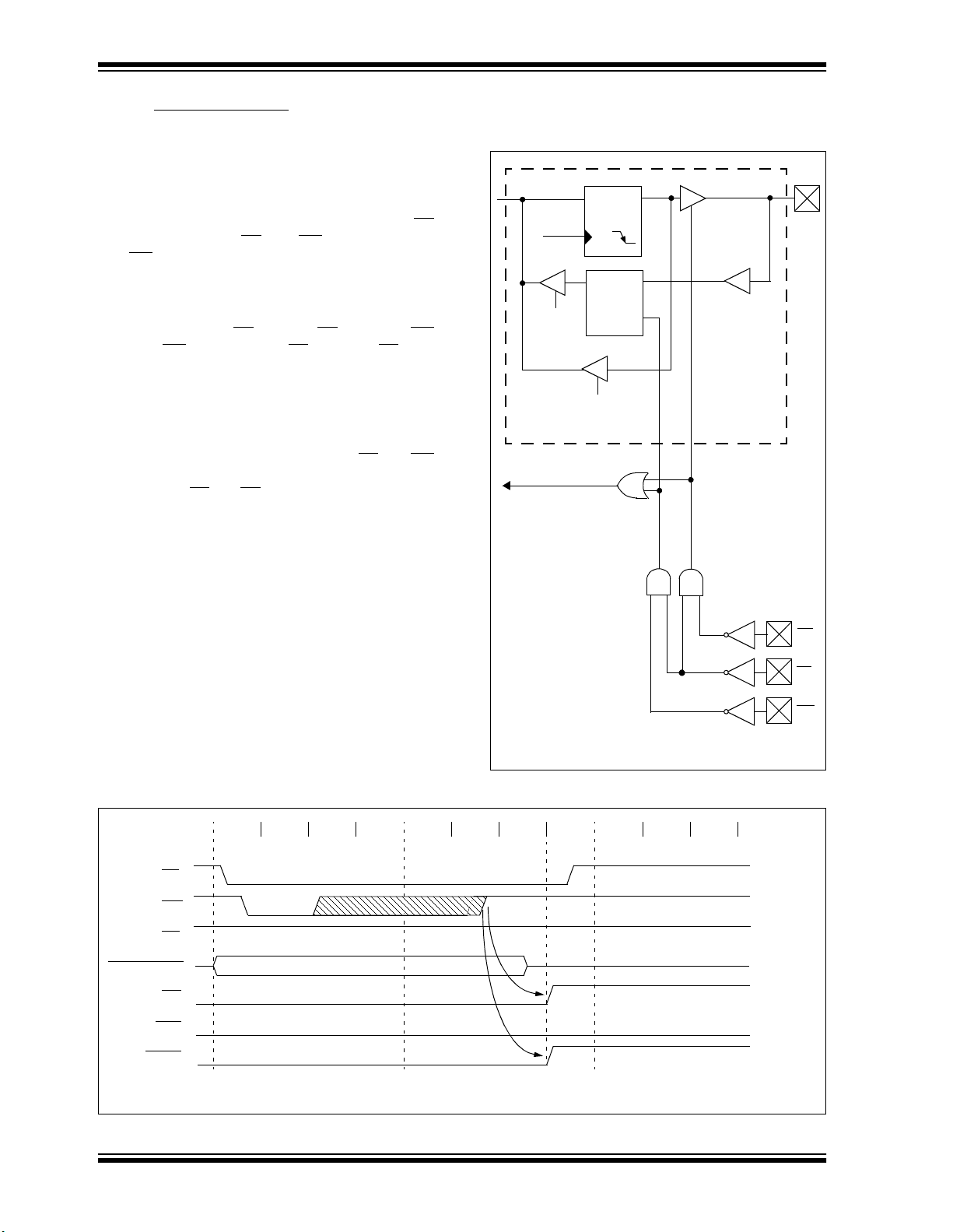
PIC18CXX2
8.6 Parallel Slave Port
The Parallel Slave Port is impleme nted on the 40 -pin
devices only (PIC18C4X2).
PORTD operates as an 8-bit wide Parallel Slave Por t,
or microprocessor port when control bit PSPMODE
(TRISE<4>) i s set. In slave mode it is asynchr onous ly
readable and writab le by the external world thro ugh RD
control input pin RE0/RD and WR control input pin
RE1/WR
It can directly interface to an 8-bit microprocessor data
bus. The e x ternal micro processo r can read or write the
PORTD latch as an 8-bit latch. Setting bit PSPMODE
enables port pin RE0/RD
to be the WR input and RE2/CS to be the CS (chip
select) input. For this functionality, the corresponding
data direction bits of the TRISE register (TRISE<2:0>)
must be configured as inputs (set). The A/D port configuration bits PCFG2:PCFG0 (ADCON1<2:0>) must
be set, which will configure pins RE2:RE0 as digital I/O.
A write to the PSP occurs when both the CS
lines are first detec ted lo w . A read from t he PSP occu rs
when both the CS
The PORTE I/O pins become control inputs for the
microprocessor port when bit PSPMODE (TRISE<4>)
is set. In this mode, the user must make sure that the
TRISE<2:0> bits are set (pins are configured as digital
inputs), and the ADCON1 is confi gured for digit al I/O. In
this mode, the input buffers are TTL.
.
to be the RD input, RE1/WR
and WR
and RD lines are first detected low.
FIGURE 8-10: PORTD AND PORTE BLOCK
DIAGRAM
(PARALLEL SLAVE PORT)
Data Bus
WR LATD
or
PORTD
RD PORTD
RD LATD
One bit of PORTD
Set Interrupt Flag
PSPIF (PIR1<7>)
QD
CK
Data Latch
QD
EN
EN
TTL
Read
Chip Select
TTL
TTL
RDx
Pin
RD
CS
Note: I/O pin has protection diodes to VDD and VSS.
FIGURE 8-11: PARALLEL SLAVE PORT WRITE WAVEFORMS
Q1 Q2 Q3 Q4CSQ1 Q2 Q3 Q4 Q1 Q2 Q3 Q4
WR
RD
PORTD<7:0>
IBF
OBF
PSPIF
Write
TTL
WR
DS39026B-page 90 Preliminary
7/99 Microchip Technology Inc.

FIGURE 8-12: PARALLEL SLAVE PORT READ WAVEFORMS
PIC18CXX2
Q1 Q2 Q3 Q4
CS
WR
RD
PORTD<7:0>
IBF
OBF
PSPIF
TABLE 8-11: REGISTERS ASSOCIATED WITH PARALLEL SLAVE PORT
Name Bit 7 Bit 6 Bit 5 Bit 4 Bit 3 Bit 2 Bit 1 Bit 0
PORTD Port data latch when written; port pins when read xxxx xxxx uuuu uuuu
LATD LATD Data Output Bits xxxx xxxx uuuu uuuu
TRISD PORTD Data Direction Bits 1111 1111 1111 1111
PORTE
LATE
TRISE IBF OBF IBOV PSPMODE
INTCON GIE/
PIR1 PSPIF
PIE1 PSPIE
IPR1 PSPIP
ADCON1
— — — — —RE2RE1RE0---- -000 ---- -000
— — — — — LATE Data Output Bits ---- -xxx ---- -uuu
GIEH
ADFM ADCS2 — — PCFG3 PCFG2 PCFG1 PCFG0 --0- -000 --0- -000
PEIE/
GIEL
ADIF RCIF TXIF SSPIF CCP 1IF TMR2IF TMR1IF 0000 0000 0000 0000
ADIE RCIE TXIE SSPIE CCP1IE TMR2IE TMR1IE 0000 0000 0000 0000
ADIP RCIP TXIP SSPIP CCP1IP TMR2IP TMR1IP 0000 0000 0000 0000
TMR0IF INT0IE RBIE TMR0IF INT0IF RBIF 0000 000x 0000 000u
Q1 Q2 Q3 Q4 Q1 Q2 Q3 Q4
Value on
POR, BOR
— PORTE Data Direction Bits 0000 -111 0000 -111
Value on all
other resets
Legend: x = unknown, u = unchanged, - = unimplemented read as ’0’.
Shaded cells are not used by the Parallel Slave Port.
7/99 Microchip Technology Inc.
Preliminary DS39026B-page 91

PIC18CXX2
NOTES:
DS39026B-page 92 Preliminary
7/99 Microchip Technology Inc.

PIC18CXX2
9.0 TIMER0 MODUL E
The Timer0 module has the following features:
• Software selectable as an 8-bit or 16-bit timer/
counter
• Readable and writable
• Dedicated 8-bit software programmable prescaler
• Clock source selectable to be external or internal
• Interrupt on overflow from FFh to 00h in 8-bit
mode and FFFFh to 0000h in 16-bit mode
• Edge select for external clock
Figure 9-1 shows a simplified block diagram of the
Timer0 module in 8-bit mode and Figure 9-1 shows a
simplified bl ock diagram of the Timer0 module in 1 6-bit
mode.
The T0CON register i s a re adab le and w ritab le reg ister
that controls all the aspects of Timer0, including the
prescale selection.
Register 9-1: T0CON: Timer0 Control Register
R/W-1 R/W-1 R/W-1 R/W-1 R/W-1 R/W-1 R/W-1 R/W-1
TMR0ON T08BIT T0CS T0SE PSA T0PS2 T0PS1 T0PS0
bit 7 bit 0
bit 7 TMR0ON: Timer0 On/Off Control bit
1 = Enables Timer0
0 = Stops Timer0
bit 6 T08BIT: Timer0 8-bit/16-bit Control bit
1 = Timer0 is configured as an 8-bit timer/counter
0 = Timer0 is configured as a 16-bit timer/counter
bit 5 T0CS: Timer0 Clock Source Select bit
1 = Transition on T0CKI pin
0 = Internal instruction cycle clock (CLKOUT)
bit 4 T0SE: Timer0 Source Edge Select bit
1 = Increment on high-t o-low transition on T0CKI pin
0 = Increment on low-to-high transition on T0CKI pin
bit 3 PSA: Timer0 Prescaler Assignment bit
1 = TImer0 prescaler is NOT assigned. Timer0 clock input bypasses prescaler
0 = Timer0 prescaler is assigned. Timer0 clock input comes from prescaler output
bit 2:0 T0PS2:T0PS0: Timer0 Prescaler Select bits
111 = 1:256 prescale value
110 = 1:128 prescale value
101 = 1:64 prescale value
100 = 1:32 prescale value
011 = 1:16 prescale value
010 = 1:8 prescale value
001 = 1:4 prescale value
000 = 1:2 prescale value
Legend:
R = Readable bit W = Writable bit U = Unimplemented bit, read as ‘0’
- n = Value at POR reset ’1’ = Bit is set ’0’ = Bit is cleared x = Bit is unknown
7/99 Microchip Technology Inc.
Preliminary DS39026B-page 93

PIC18CXX2
FIGURE 9-1: TIMER0 BLOCK DIAGRAM IN 8-BIT MODE
FOSC/4
RA4/T0CKI
Pin
T0SE
Note: Upon reset, Timer0 is enabled in 8-bit mode with clock input from T0CKI max. prescale.
FIGURE 9-2: TIMER0 BLOCK DIAGRAM IN 16-BIT MODE
0
1
T0PS2, T0PS1, T0PS0
T0CS
Programmable
Prescaler
3
0
1
PSA
Sync with
Internal
clocks
(2 Tcy delay)
Data Bus
8
TMR0
Set Interrupt
Flag bit TMR0IF
on overflow
FOSC/4
T0CKI pin
T0SE
0
1
Programmable
Prescaler
T0PS2, T0PS1, T0PS0
T0CS
0
1
3
PSA
Sync with
Internal
Clocks
(2 Tcy delay)
TMR0L
8
Note: Upon reset, Timer0 is enabled in 8-bit mode with clock input from T0CKI max. prescale.
TMR0
High Byte
8
TMR0H
8
8
Read TMR0L
Write TMR0L
Data Bus<7:0>
Set Interrupt
Flag bit TMR0IF
on overflow
DS39026B-page 94 Preliminary
7/99 Microchip Technology Inc.
PIC18CXX2
9.1 Timer0 Operation
Timer0 can operate as a timer or as a counter.
Timer mode is selected by clearing the T0CS bit. In
timer mode, the Timer0 module will increment every
instruction cycl e (with out prescaler). If the TMR0 register is written, the increment i s inhibite d f o r the f oll owin g
two instruction cycles. The user can work around this
by writing an adjusted value to the TMR0 register.
Counter mode is selected by setting the T0CS bit. In
counter mode, Timer0 will increment either on every
rising or fal ling e dge o f pin RA4/T0 CKI. The in creme nting edge is determined by the Timer0 Source Edge
Select bit (T0SE). Clearing the T0SE bit selec ts the rising edge. Restrictions on the external clock input are
discussed be low.
When an ex ternal clock i nput is used f or Timer0 , it must
meet certain requirements. The requirements ensure
the external c lock can be synchron ized w ith the int ernal
phase clock (T
incrementing of Timer0 after synchronization.
OSC). Also, there is a delay in the actual
9.2 Prescaler
An 8-bit counter is available as a prescaler for the
Timer0 modul e. The presca ler is not readable or wr itable.
The PSA and T0PS2:T0PS0 bits determine the prescaler assignment and prescale ratio.
Clearing bit PSA will assign the prescaler to the Timer0
module. When the prescaler is assigned to the Timer0
module, prescale values of 1:2, 1:4, ..., 1:256 are
selectable.
When assigned to the Ti mer0 mo dul e, all in str u cti on s
writing to the TMR0 register (e.g. CLRF TMR0,
MOVWF TMR0, BSF TMR0, x....etc.) will clear the
prescaler count.
9.2.1 SWITCHING PRESCALER ASSIGNMENT The prescaler assignment is fully under software con-
trol, (i.e., it can be change d “on- the-fly ” during progr am
ex ecutio n).
9.3 Timer0 Interrupt
The TMR0 interrupt is generated when the TMR0 register overflo w s from FFh to 00h in 8-bit mod e or FFFFh
to 0000h in 16-bit mode. This ov erflow s ets the T MR0IF
bit. The interrupt can be masked by clearing the
TMR0IE bit. The TMR0IE bit must be cleared in software by the Timer0 module interrupt service routine
before re-enabling this interrupt. The TMR0 interrupt
cannot awaken the processor from SLEEP, since the
timer is shut off during SLEEP.
9.4 16-Bit Mode Timer Reads and Writes
TMR0H is not the high byte of the timer/counter in 16bit mode, but is actually a buffered version of the high
byte of Timer0 (refer to Figure 9-1). The high byte of
the Timer0 counter/timer is not directly readable nor
writable. TMR0H is updated with the contents of the
high byte of T imer0 during a read of TMR0L. This p r ovides the ability to read all 16-bits of Timer0 without
having to veri fy that t he read of the high and l ow byte
were valid due to a rollover between successive reads
of the high and low byte.
A write to the high byte of Timer0 must also take place
through the TMR0H b uff er register. Timer0 high byte is
updated with the contents of TMR0H when a write
occurs to TMR0L. This allows all 16 bits of Timer0 to
be updated at once.
Note: Writing to TMR0 when the prescaler is
assigned to Timer0 will clear the prescaler
count, but will not change the prescaler
assignment.
TABLE 9-1: REGISTERS ASSOCIATED WITH TIMER0
Name Bit 7 Bit 6 Bit 5 Bit 4 Bit 3 Bit 2 Bit 1 Bit 0
TMR0L Timer0 Module’s Low Byte Register
TMR0H Timer0 Module’s High Byte Register
INTCON GIE/GIEH PEIE/GIEL TMR0IE INT0IE RBIE TMR0IF INT0IF RBIF
T0CON TMR0ON T08BIT T0CS T0SE PSA T0PS2 T0PS1 T0PS0
TRISA — — PORTA Data Direction Register
Legend: x = unknown, u = unchanged, - = unimplemented locations read as '0'.
Shaded cells are not used by Timer0.
7/99 Microchip Technology Inc.
Preliminary DS39026B-page 95
Value on
POR, BOR
xxxx xxxx uuuu uuuu
0000 0000 0000 0000
0000 000x 0000 000u
1111 1111 1111 1111
--11 1111 --11 1111
Valu e on a ll
other resets

PIC18CXX2
NOTES:
DS39026B-page 96 Preliminary
7/99 Microchip Technology Inc.

PIC18CXX2
10.0 TIMER1 MODULE
The Timer1 module timer/co unter has th e fol lowing f eatures:
• 16-bit timer/counter
(Two 8-bit registers; TMR1H and TMR1L)
• Readable and writable (Both registers)
• Internal or external clock select
• Interrupt on overflow from FFFFh to 0000h
• Reset from CCP module special event trigger
Figure 10-1 is a simplified block diagram of the Timer1
module.
Register 10-1 shows the Timer1 contro l register. This
register controls the operating mode of the Timer1
module as wel l as contai ns the Time r1 oscillat or enabl e
bit (T1OSCEN). Timer1 can be enabled/disabled by
setting/clearing control bit TMR1ON (T1CON<0>).
Register 10-1: T1CON: Timer1 Control Register
R/W-0 U-0 R/W-0 R/W-0 R/W-0 R/W-0 R/W-0 R/W-0
RD16
bit 7 bit 0
bit 7 RD16: 16-bit Read/Write Mode Enable bit
1 = Enables register Read/Write of TImer1 in one 16-bit operation
0 = Enables register Read/Write of Timer1 in two 8-bit operations
bit 6 Unimplemented: Read as '0'
bit 5:4 T1CKPS1:T1CKPS0: Timer1 Input Clock Prescale Select bits
11 = 1:8 Prescale value
10 = 1:4 Prescale value
01 = 1:2 Prescale value
00 = 1:1 Prescale value
bit 3 T1OSCEN: Timer1 Oscillator Enable bit
1 = Timer1 Oscillator is enabled
0 = Timer1 Oscillator is shut off.
The oscillator inverter and feedback resistor are turned off to eliminate power drain
bit 2 T1SYNC
When TMR1CS = 1:
1 = Do not synchronize external clock input
0 = Synchronize external clock input
When TMR1CS = 0:
This bit is ignored. Timer1 uses the internal clock when TMR1CS = 0.
bit 1 TMR1CS: Timer1 Clock Source Select bit
1 = External clock from pin RC0/T1OSO/T13CKI (on the rising edge)
0 = Internal clock (F
bit 0 TMR1ON: Timer1 On bit
1 = Enables Timer1
0 = Stops Timer1
— T1CKPS1 T1CKPS0 T1OSCEN T1SYNC TMR1CS TMR1ON
: Timer1 External Clock Input Synchronization Select bit
OSC/4)
Legend:
R = Readable bit W = Writable bit U = Unimplemented bit, read as ‘0’
- n = Value at POR reset ’1’ = Bit is set ’0’ = Bit is cleared x = Bit is unknown
7/99 Microchip Technology Inc.
Preliminary DS39026B-page 97

PIC18CXX2
10.1 Timer1 Operation
Timer1 can operate in one of these modes:
•As a timer
• As a synchronous counter
• As an asynchronous counter
The operating mode is determined by the clock select
bit, TMR1CS (T1CON<1>).
FIGURE 10-1: TIMER1 BLOCK DIAGRAM
TMR1IF
Overflow
Interrupt
Flag Bit
T1CKI/T1OSO
T1OSI
TMR1H
T1OSC
TMR1
TMR1L
T1OSCEN
Enable
Oscillator
CLR
(1)
CCP Special Event Trigger
TMR1ON
on/off
FOSC/4
Internal
Clock
When TMR1CS = 0, Timer1 increments every instruction cycle. When TMR1CS = 1, Timer1 increments on
every rising edge of the external clock input or the
Timer1 oscillator, if enabled.
When the Timer1 oscillator is enabled (T1OSCEN is
set), the RC1/T1OSI and RC0/T1OSO/T1CKI pins
become inputs. That is, the TRISC<1:0> value is
ignored.
Timer1 also has an in ternal “reset input ”. This reset can
be generated by the CCP module (Section 13.0).
Synchronized
Clock Input
Synchronize
det
SLEEP input
1
0
T1CKPS1:T1CKPS0
TMR1CS
0
1
T1SYNC
Prescaler
1, 2, 4, 8
2
Note 1: When enable bit T1OSCEN is cleared, the inverter and feedback resistor are turned off. This
eliminates power drain.
FIGURE 10-2: TIMER1 BLOCK DIAGRAM: 16-BIT READ/WRITE MODE
Data bus<7:0>
8
TMR1H
8
Write TMR1L
Read TMR1L
TMR1IF
Overflow
Interrupt
flag bit
T13CKI/T1OSO
T1OSI
8
Timer 1
high byte
T1OSC
TMR1
Note1: When enable bit T1OSCEN is cleared, the inverter and feedback resistor are turned off. This eliminates
power drain.
8
TMR1L
T1OSCEN
Enable
Oscillator
0
1
TMR1ON
on/off
1
Fosc/4
(1)
Internal
Clock
0
TMR1CS
T1SYNC
Prescaler
1, 2, 4, 8
2
T1CKPS1:T1CKPS0
Synchronized
clock input
Synchronize
det
SLEEP input
DS39026B-page 98 Preliminary
7/99 Microchip Technology Inc.

PIC18CXX2
10.2 Timer1 Oscillator
A crystal oscillator circuit is bu ilt-in between pins T1OSI
(input) and T1OSO (amplifier output). It is enabled by
setting control bit T1OSCEN (T 1CON<3>). The oscill ator is a low power oscillator rated up to 200 kHz. It will
continue to run during SLEEP. It is primarily intended
for a 32 kHz crystal. Table 10-1 shows the capacitor
selection for the Timer1 oscillator.
The user must provide a software time delay to ensure
proper start-up of the Timer1 oscill ator.
TABLE 10-1: CAPACITOR SELECTION FOR
THE ALTERNATE OSCILLATOR
Osc Type Freq C1 C2
(1)
LP 32 kHz TBD
Crystal to be Tested:
32.768 kHz Epson C-001R32.768K-A ± 20
Note1: Microchip suggests 33 pF as a starting
point in validating the oscillator circuit.
2: Higher capacitance increases the stability
of the oscillator, but also increases the
start-up time.
3: Since each resonator/crystal has its own
characteristics, the user should consult the
resonator/crystal manufacturer for appropriate values of external components.
4: Capacitor values are for design guidance
only.
TBD
PPM
(1)
10.3 Timer1 Interrupt
The TMR1 Register pair (TMR1H:TMR1L) increments
from 0000h to FFFFh and rolls over to 0000h. The
TMR1 Interrupt, if enabled, is generated on overflow,
which is latched in interrupt flag bit TMR1IF (PI R1<0>).
This interrupt can be enab led/d isab led by se tting/cle aring TMR1 interrupt enable bit TMR1IE (PIE1<0>).
10.4 Resetting Timer1 using a CCP Trigger Output
If the CCP module is configured in compare mode to
generate a “special event trigger" (CCP1M3:CCP1M0
= 1011), this signal will reset Timer1 and start an A/D
conversion (if the A/D module is enabled).
Note: The special event triggers from the CCP1
module will not set interrupt flag bit
TMR1IF (PIR1<0>).
Timer1 must be configured for either timer or synchronized counter mode to tak e adv antage of this fea ture . If
Timer1 is running in asynchronous counter mode, this
reset operation may not work.
In the ev ent that a write to Timer1 coinc ides with a sp ecial event trigger from CCP1, the write will take precedence.
In this mode of operati on, the CC PR1H:CCPR 1L regis ters pair effectively becomes the period register for
Timer1.
10.5 Timer1 16-Bit Read/Write Mode
Timer1 can be configured for 16-bit reads and writes
(see Figure 10-2). When the RD16 control bit
(T1CON<7>) is set, the address for TMR1H is mapped
to a buffer register for the high byte of Timer1. A read
from TMR1L w ill load the cont ents of th e high byte o f
Timer1 into the Timer1 high byte buffer. This provides
the user with the ability to accurately read all 16-bits of
Timer1 without having to determine whether a read of
the high byte followed by a read of the low byte is valid
due to a rollover between reads.
A write to the high byte of Timer1 must also take place
through the TMR1H b uff er register. Timer1 high byte is
updated with the contents of TMR1H when a write
occurs to TMR1L. This allo ws a u ser to write all 16 bits
to both the high and low bytes of Timer1 at once.
The high byte of Ti mer1 is not directly readable or writable in this mode . All rea ds an d writes m ust tak e pl ace
through the Timer1 high byte buffer register. Writes to
TMR1H do not clear the Timer1 prescaler. The prescaler is only cleared on writes to TMR1L.
7/99 Microchip Technology Inc.
Preliminary DS39026B-page 99

PIC18CXX2
TABLE 10-2: REGISTERS ASSOCIATED WITH TIMER1 AS A TIMER/COUNTER
Value on
POR,
Name Bit 7 Bit 6 Bit 5 Bit 4 Bit 3 Bit 2 Bit 1 Bit 0
INTCON GIE/
GIEH
PIR1
PIE1
IPR1
TMR1L Holding register for the Least Significant Byte of the 16-bit TMR1 register xxxx xxxx uuuu uuuu
TMR1H Holding register for the Most Significant Byte of the 16-bit TMR1 register xxxx xxxx uuuu uuuu
T1CON
PSPIF
PSPIE
PSPIP
— — T1CKPS1 T1CKPS0 T1OSCEN T1SYNC TMR1CS TMR1ON --00 0000 --uu uuuu
PEIE/
GIEL
(1)
ADIF RCIF TXIF SSPIF CCP1IF TM R2IF TMR1IF 0000 0000 0000 0000
(1)
ADIE RCIE TXIE SSPIE CCP1IE TMR2IE TMR1IE 0000 0000 0000 0000
(1)
ADIP RCIP TXIP SSPIP CCP1IP TMR2IP TMR1IP 0000 0000 0000 0000
TMR0IE INT0IE RBIE TMR0IF INT0IF RBIF 0000 000x 0000 000u
BOR
Legend: x = unknown, u = unchanged, - = unimplemented read as ’0’.
Shaded cel ls are not used by the Timer1 module.
Note1: The PSPIF, PSPIE and PSPIP bits are reserved on the PIC18C2X2 devices. Always maintain these bits clear.
Value on
all other
resets
DS39026B-page 100 Preliminary
7/99 Microchip Technology Inc.
 Loading...