

Microchip Technology Inc PIC17C752-08-PT, PIC17C752-08-SP, PIC17C752-08I-JW, PIC17C752-08I-L, PIC17C752-08I-P Datasheet
...
1997 Microchip Technology Inc.
Preliminary
DS30264A-page 1
Devices included in this data sheet:
• PIC17C752
• PIC17C756
Microcontroller Core Features:
• Only 58 single word instructions to learn
• All single cycle instructions (121 ns) except for
program branches and table reads/writes which
are two-cycle
• Operating speed:
- DC - 33 MHz clock input
- DC - 121 ns instruction cycle
• Hardware Multiplier
• Interrupt capability
• 16 level deep hardware stack
• Direct, indirect, and relative addressing modes
• Internal/external program memory execution
• Capable of addressing 64K x 16 program memory
space
Peripheral Features:
• 50 I/O pins with individual direction control
• High current sink/source for direct LED drive
- RA2 and RA3 are open drain, high voltage
(12V), high current (60 mA), I/O pins
• Four capture input pins
- Captures are 16-bit, max resolution 121 ns
• Three PWM outputs
- PWM resolution is 1- to 10-bits
• TMR0: 16-bit timer/counter with
8-bit programmable prescaler
• TMR1: 8-bit timer/counter
• TMR2: 8-bit timer/counter
• TMR3: 16-bit timer/counter
• Two Universal Synchronous Asynchronous
Receiver Transmitters (USART/SCI)
- Independant baud rate generators
• 10-bit, 12 channel analog-to-digital converter
• Synchronous Serial Port (SSP) with SPI™ and
I
2
C™ modes (including I
2
C master mode)
Device
Memory
Program (x16) Data (x8)
PIC17C752 8K 454
PIC17C756 16K 902
✯
✯
Pin Diagrams
Special Microcontroller Features:
• Power-on Reset (POR), Power-up Timer (PWRT)
and Oscillator Start-up Timer (OST)
• Watchdog Timer (WDT) with its own on-chip RC
oscillator for reliable operation
• Brown-out Reset
• Code-protection
• Power saving SLEEP mode
• Selectable oscillator options
CMOS Technology:
• Low-power, high-speed CMOS EPROM
technology
• Fully static design
• Wide operating voltage range (2.5V to 6.0V)
• Commercial and Industrial temperature ranges
• Low-power consumption
- < 5 mA @ 5V, 4 MHz
- 100 µ A typical @ 4.5V, 32 kHz
- < 1 µ A typical standby current @ 5V
987654321
68676665646362
61
RD2/AD10
RD3/AD11
RD4/AD12
RD5/AD13
RD6/AD14
RD7/AD15
RC0/AD0
VDDNC
V
SS
RC1/AD1
RC2/AD2
RC3/AD3
RC4/AD4
RC5/AD5
RC6/AD6
RC7/AD7
10
11
12
13
14
15
16
17
18
19
20
21
22
23
24
25
26
60
59
58
57
56
55
54
53
52
51
50
49
48
47
46
45
44
2728293031323334353637383940414243
PIC17C75X
RA0/INT
RB0/CAP1
RB1/CAP2
RB3/PWM2
RB4/TCLK12
RB5/TCLK3
RB2/PWM1
V
SS
NC
OSC2/CLKOUT
OSC1/CLKIN
V
DD
RB7/SDO
RA3/SDI/SDA
RA2/SS
/SCL
RA1/T0CKI
RD1/AD9
RD0/AD8
RE0/ALE
RE1/OE
RE2/WR
RE3/CAP4
MCLR
/VPP
TEST
V
SS
VDD
RF7/AN11
RF6/AN10
RF5/AN9
RF4/AN8
RF3/AN7
RF2/AN6
RF1/AN5
RF0/AN4
AV
DD
AVSS
RG3/AN0/VREF+
RG2/AN1/V
REF-
RG1/AN2
RG0/AN3
NC
V
SS
VDD
RG4/CAP3
RG5/PWM3
RG7/TX2/CK2
RG6/RX2/DT2
RA4/RX1/DT1
RA5/TX1/CK1
NC
RB6/SCK
LCC
Top View
PIC17C75X
High-Performance 8-Bit CMOS EPROM Microcontrollers

PIC17C75X
DS30264A-page 2
Preliminary
1997 Microchip Technology Inc.
Pin Diagrams Cont.’d
PIC17C75X IN 68-PIN LCC
10
11
12
13
14
15
16
17
18
19
20
21
22
23
24
25
26
60
59
58
57
56
55
54
53
52
51
50
49
48
47
46
45
44
987654321
68676665646362
61
2728293031323334353637383940414243
Top View
RA0/INT
RB0/CAP1
RB1/CAP2
RB3/PWM2
RB4/TCLK12
RB5/TCLK3
RB2/PWM1
V
SS
NC
OSC2/CLKOUT
OSC1/CLKIN
V
DD
RB7/SDO
RA3/SDI/SDA
RA2/SS
/SCL
RA1/T0CKI
RD1/AD9
RD0/AD8
RE0/ALE
RE1/OE
RE2/WR
RE3/CAP4
MCLR
/VPP
TEST
V
SS
VDD
RF7/AN11
RF6/AN10
RF5/AN9
RF4/AN8
RF3/AN7
RF2/AN6
RD2/AD10
RD3/AD11
RD4/AD12
RD5/AD13
RD6/AD14
RD7/AD15
RC0/AD0
VDDNC
VSS
RC1/AD1
RC2/AD2
RC3/AD3
RC4/AD4
RC5/AD5
RC6/AD6
RC7/AD7
RF1/AN5
RF0/AN4
AV
DD
AVSS
RG3/AN0/VREF+
RG2/AN1/V
REF-
RG1/AN2
RG0/AN3
NC
V
SS
VDD
RG4/CAP3
RG5/PWM3
RG7/TX2/CK2
RG6/RX2/DT2
RA4/RX1/DT1
RA5/TX1/CK1
NC
RB6/SCK
PIC17C75X
1997 Microchip Technology Inc.
Preliminary
DS30264A-page 3
PIC17C75X
Pin Diagrams Cont.’d
PIC17C75X IN 64-PIN TQFP
Pin Diagrams Cont.’d
PIC17C75X IN 64-PIN Y-SHRINK DIP
1
2
3
4
5
6
7
8
9
10
11
12
13
14
15
16
48
47
46
45
44
43
42
41
40
39
38
37
36
35
34
33
646362616059585756555453525150
49
171819202122232425262728293031
32
Top View
Applicable to 14 x 14 mm TQFP
RD2/AD10
RD3/AD11
RD4/AD12
RD5/AD13
RD6/AD14
RD7/AD15
RC0/AD0
VDDVSS
RC1/AD1
RC2/AD2
RC3/AD3
RC4/AD4
RC5/AD5
RC6/AD6
RC7/AD7
RD1/AD9
RD0/AD8
RE0/ALE
RE1/OE
RE2/WR
RE3/CAP4
MCLR
/VPP
TEST
V
SS
VDD
RF7/AN11
RF6/AN10
RF5/AN9
RF4/AN8
RF3/AN7
RF2/AN6
RA0/INT
RB0/CAP1
RB1/CAP2
RB3/PWM2
RB4/TCLK12
RB5/TCLK3
RB2/PWM1
V
SS
OSC2/CLKOUT
OSC1/CLKIN
VDD
RB7/SDO
RA3/SDI/SDA
RA2/SS
/SCL
RA1/T0CKI
RF1/AN5
RF0/AN4
AV
DD
AVSS
RG3/AN0/VREF+
RG2/AN1/V
REF-
RG1/AN2
RG0/AN3
V
SS
VDD
RG4/CAP3
RG5/PWM3
RG7/TX2/CK2
RG6/RX2/DT2
RA4/RX1/DT1
RA5/TX1/CK1
RB6/SCK
PIC17C75X
1
2
3
4
5
6
7
8
9
10
11
12
13
14
15
16
17
18
19
20
64
63
62
61
60
59
58
57
56
55
54
53
52
51
50
49
48
47
46
45
PIC17C75X
44
43
42
41
40
39
21
22
23
24
25
26
27
28
29
30
31
32
38
37
36
35
34
33
VDD
RC0/AD0
RD7/AD15
RD6/AD14
RD5/AD13
RD4/AD12
RD3/AD11
RD2/AD10
RD1/AD9
RD0/AD8
RE0/ALE
RE1/OE
RE2/WR
RE3/CAP4
MCLR
/VPP
TEST
V
DD
RF7/AN11
RF6/AN10
RF5/AN9
RF4/AN8
RF3/AN7
RF2/AN6
RF1/AN5
RF0/AN4
AV
SS
AVDD
RG3/AN0/VREF+
RG2/AN1/V
REF-
RG1/AN2
V
SS
VSS
RC1/AD1
RC2/AD2
RC3/AD3
RC4/AD4
RC5/AD5
RC6/AD6
RC7/AD7
RA0/INT
RB0/CAP1
RB1/CAP2
RB3/PWM2
RB4/TCLK12
RB5/TCLK3
RB2/PWM1
V
SS
OSC2/CLKOUT
OSC1/CLKIN
V
DD
RB7/SDO
RB6/SCK
RA2/SS/SCL
RA1/T0CKI
RA4/RX1/DT1
RA5/TX1/CK1
RG6/RX2/DT2
RG7/TX2/CK2
RG5/PWM3
RG4/CAP3
V
DD
VSS
RG0/AN3
RA3/SDI/SDA

PIC17C75X
DS30264A-page 4
Preliminary
1997 Microchip Technology Inc.
Table of Contents
1.0 Overview........................................................................................................................................................................................ 5
2.0 Device Varieties............................................................................................................................................................................. 7
3.0 Architectural Overview................................................................................................................................................................... 9
4.0 On-chip Oscillator Circuit ............................................................................................................................................................. 15
5.0 Reset............................................................................................................................................................................................ 21
6.0 Interrupts......................................................................................................................................................................................29
7.0 Memory Organization................................................................................................................................................................... 39
8.0 Table Reads and Table Writes .................................................................................................................................................... 55
9.0 Hardware Multiplier...................................................................................................................................................................... 61
10.0 I/O Ports....................................................................................................................................................................................... 65
11.0 Overview of Timer resources ....................................................................................................................................................... 85
12.0 Timer0.......................................................................................................................................................................................... 87
13.0 Timer1, Timer2, Timer3, PWMs and Captures ............................................................................................................................ 91
14.0 Universal Synchronous Asynchronous Receiver Transmitter (USART) Modules......................................................................107
15.0 Synchronous Serial Port (SSP) Module..................................................................................................................................... 123
16.0 Analog-to-Digital Converter (A/D) Module ................................................................................................................................. 167
17.0 Special Features of the CPU ..................................................................................................................................................... 177
18.0 Instruction Set Summary............................................................................................................................................................183
19.0 Development Support ................................................................................................................................................................ 219
20.0 PIC17C752/756 Electrical Characteristics................................................................................................................................. 223
21.0 PIC17C752/756 DC and AC Characteristics ............................................................................................................................. 249
22.0 Packaging Information ............................................................................................................................................................... 261
Appendix A: Modifications..............................................................................................................................................................265
Appendix B: Compatibility .............................................................................................................................................................. 265
Appendix C: What’s New................................................................................................................................................................ 266
Appendix D: What’s Changed........................................................................................................................................................ 266
Appendix E: I
2
C
Overview...........................................................................................................................................................267
Appendix F: Status and Control Registers..................................................................................................................................... 273
Appendix G: PIC16/17 Microcontrollers ......................................................................................................................................... 293
Pin Compatibility ................................................................................................................................................................................ 302
Index .................................................................................................................................................................................................. 303
On-Line Support................................................................................................................................................................................. 317
Reader Response.............................................................................................................................................................................. 318
PIC17C75X Product Identification System......................................................................................................................................... 319
To Our Valued Customers
We constantly strive to improve the quality of all our products and documentation. We have spent an excep-
tional amount of time to ensure that these documents are correct. However, we realize that we may have
missed a few things. If you find any information that is missing or appears in error, please use the reader
response form in the back of this data sheet to inform us. We appreciate your assistance in making this a better document.

1997 Microchip Technology Inc.
Preliminary
DS30264A-page 5
PIC17C75X
1.0 OVERVIEW
This data sheet covers the PIC17C75X group of the
PIC17CXXX family of microcontrollers. The following
devices are discussed in this data sheet:
• PIC17C752
• PIC17C756
The PIC17C75X devices are 68-Pin, EPROM-based
members of the versatile PIC17CXXX family of
low-cost, high-performance, CMOS, fully-static, 8-bit
microcontrollers.
All PIC16/17 microcontrollers employ an advanced
RISC architecture. The PIC17CXXX has enhanced
core features, 16-lev el deep stack, and multiple internal
and external interrupt sources. The separate instruction and data buses of the Harvard architecture allow a
16-bit wide instruction word with a separate 8-bit wide
data path. The two stage instruction pipeline allows all
instructions to execute in a single cycle, e xcept for program branches (which require two cycles). A total of 58
instructions (reduced instruction set) are available.
Additionally, a large register set gives some of the
architectural innovations used to achieve a very high
performance. For mathematical intensive applications
all devices have a single cycle 8 x 8 Hardware Multiplier.
PIC17CXXX microcontrollers typically achieve a 2:1
code compression and a 4:1 speed improvement over
other 8-bit microcontrollers in their class.
PIC17C75X devices have up to 902 bytes of RAM and
50 I/O pins. In addition, the PIC17C75X adds several
peripheral features useful in many high performance
applications including:
• Four timer/counters
• Four capture inputs
• Three PWM outputs
• Two independant Universal Synchronous Asynchronous Receiver Transmitters (USARTs)
• An A/D converter (12 channel, 10-bit resolution)
• A Synchronous Serial Port
(SPI and I
2
C w/ Master mode)
These special features reduce external components,
thus reducing cost, enhancing system reliability and
reducing power consumption.
There are four oscillator options, of which the single pin
RC oscillator provides a low-cost solution, the LF oscillator is for low frequency crystals and minimizes power
consumption, XT is a standard crystal, and the EC is for
external clock input.
The SLEEP (power-down) mode offers additional
power saving. W ak e-up from SLEEP can occur through
several external and internal interrupts and device
resets.
A highly reliable Watchdog Timer with its own on-chip
RC oscillator provides protection against software malfunction.
There are four configuration options for the device
operational mode:
• Microprocessor
• Microcontroller
• Extended microcontroller
• Protected microcontroller
The microprocessor and extended microcontroller
modes allow up to 64K-words of external program
memory.
Brown-out Reset circuitry has also been added to the
device. This allo ws a device reset to occur if the device
V
DD
falls below the Brown-out voltage trip point
(BV
DD
). The chip will remain in Brown-out Reset until
V
DD
rises above BV
DD
.
Table 1-1 lists the features of the PIC17CXXX devices.
A UV-erasable CERQUAD-packaged version (compat-
ible with PLCC) is ideal for code de velopment while the
cost-effective One-Time Programmable (OTP) version
is suitable for production in any volume.
The PIC17C75X fits perfectly in applications that
require extremely fast execution of complex software
programs. These include applications ranging from
precise motor control and industrial process control to
automotive, instrumentation, and telecom applications.
The EPROM technology makes customization of application programs (with unique security codes, combinations, model numbers, parameter storage, etc.) fast
and convenient. Small footprint package options
(including die sales) make the PIC17C75X ideal for
applications with space limitations that require high
performance.
An In-circuit Serial Programming (ISP) feature allows:
• Flexibility of programming the software code as
one of the last steps of the manufacturing process
High speed execution, powerful peripheral features,
flexible I/O, and low power consumption all at low cost
make the PIC17C75X ideal for a wide range of embedded control applications.
1.1 Family and
Upward Compatibility
The PIC17CXXX family of microcontrollers have architectural enhancements over the PIC16C5X and
PIC16CXX families. These enhancements allow the
device to be more efficient in software and hardware
requirements. Refer to Appendix A for a detailed list of
enhancements and modifications. Code written for
PIC16C5X or PIC16CXX can be easily ported to
PIC17CXXX devices (Appendix B).
1.2 Development Support
The PIC17CXXX family is supported by a full-featured
macro assembler, a software simulator, an in-circuit
emulator, a universal programmer, a “C” compiler, and
fuzzy logic support tools. For additional inf ormation see
Section 19.0.
PIC17C75X
DS30264A-page 6
Preliminary
1997 Microchip Technology Inc.
TABLE 1-1: PIC17CXXX FAMILY OF DEVICES
Features PIC17CR42 PIC17C42A PIC17C43 PIC17CR43 PIC17C44 PIC17C752 PIC17C756
Maximum Frequency
of Operation
33 MHz 33 MHz 33 MHz 33 MHz 33 MHz 33 MHz 33 MHz
Operating V oltage Range 2.5 - 6.0V 2.5 - 6.0V 2.5 - 6.0V 2.5 - 6.0V 2.5 - 6.0V 3.0 - 6.0V 3.0 - 6.0V
Program Memory
( x16)
(EPROM) - 16 K 4K - 8K 8K 16K
(ROM) 2K - - 4K --Data Memory (bytes) 232 232 454 454 454 454 902
Hardware Multiplier (8 x 8) Yes Yes Yes Yes Yes Yes Yes
Timer0
(16-bit + 8-bit postscaler)
Yes Yes Yes Yes Yes Yes Yes
Timer1 (8-bit) Yes Yes Yes Yes Yes Yes Yes
Timer2 (8-bit) Yes Yes Yes Yes Yes Yes Yes
Timer3 (16-bit) Yes Yes Yes Yes Yes Yes Yes
Capture inputs (16-bit) 2 2 2 2 244
PWM outputs (up to 10-bit) 2 2 2 2 233
USART/SCI 1 1 1 1 122
A/D channels (10-bit) - - - - -1212
SSP (SPI/I
2
C w/Master mode)
- - - - - Yes Yes
Power-on Reset
Yes Yes Yes Yes Yes Yes Yes
Watchdog Timer Yes Yes Yes Yes Yes Yes Yes
External Interrupts Yes Yes Yes Yes Yes Yes Yes
Interrupt Sources 11 11 11 11 11 18 18
Code Protect Yes Yes Yes Yes Yes Yes Yes
Brown-out Reset - - - - - Yes Yes
In-circuit Serial Programming - - - - - Yes Yes
I/O Pins 33 33 33 33 33 50 50
I/O High Current
Capability
Source 25 mA 25 mA 25 mA 25 mA 25 mA 25 mA 25 mA
Sink
25 mA
(1)
25 mA
(1)
25 mA
(1)
25 mA
(1)
25 mA
(1)
25 mA
(1)
25 mA
(1)
Package Types
40-pin DIP
44-pin PLCC
44-pin MQFP
44-pin TQFP
40-pin DIP
44-pin PLCC
44-pin MQFP
44-pin TQFP
40-pin DIP
44-pin PLCC
44-pin MQFP
44-pin TQFP
40-pin DIP
44-pin PLCC
44-pin MQFP
44-pin TQFP
40-pin DIP
44-pin PLCC
44-pin MQFP
44-pin TQFP
64-pin DIP
68-pin LCC
68-pin TQFP
64-pin DIP
68-pin LCC
68-pin TQFP
Note 1: Pins RA2 and RA3 can sink up to 60 mA.
1997 Microchip Technology Inc.
Preliminary
DS30264A-page 7
PIC17C75X
2.0 DEVICE VARIETIES
Each device has a variety of frequency ranges and
packaging options. Depending on application and production requirements, the proper device option can be
selected using the information in the PIC17C75X Product Selection System section at the end of this data
sheet. When placing orders, please use the
“PIC17C75X Product Identification System” at the back
of this data sheet to specify the correct part number.
When discussing the functionality of the device, memory technology and voltage range does not matter.
There are three memory type options. These are specified in the middle characters of the part number.
1. C , as in PIC17 C 756. These devices have
EPROM type memory.
2. CR , as in PIC17 CR 756. These devices have
ROM type memory.
3. F , as in PIC17 F 756. These devices have Flash
type memory.
All these devices operate over the standard voltage
range. Devices are also offered which operate over an
extended voltage range (and reduced frequency
range). Table 2-1 shows all possible memory types and
voltage range designators for a particular device.
These designators are in bold typeface.
TABLE 2-1: DEVICE MEMORY
VARIETIES
Memory T ype
Voltage Range
Standard Extended
EPROM PIC17
C
XXX PIC17
LC
XXX
ROM
PIC17
CR
XXX PIC17
LCR
XXX
Flash
PIC17FXXX PIC17LFXXX
Note: Not all memory technologies are available
for a particular device.
2.1 UV Erasable Devices
The UV erasable version, offered in CERQUAD package, is optimal for prototype dev elopment and pilot programs.
The UV erasable version can be erased and reprogrammed to any of the configuration modes.
Microchip's programming of the PIC17C75X. Third
party programmers also are available; ref er to the
Third
Party Guide
for a list of sources.
2.2 One-Time-Programmable (OTP)
Devices
The availability of OTP devices is especially useful for
customers expecting frequent code changes and
updates.
The OTP devices, packaged in plastic packages, permit the user to program them once. In addition to the
program memory, the configuration bits must be programmed.
2.3 Quick-Turnaround-Production (QTP)
Devices
Microchip offers a QTP Programming Service for factory production orders. This service is made available
for users who choose not to program a medium to high
quantity of units and whose code patterns have stabilized. The devices are identical to the OTP devices but
with all EPROM locations and configuration options
already programmed by the factory. Certain code and
prototype verification procedures apply before production shipments are available. Please contact your local
Microchip Technology sales office for more details.
2.4 Serialized Quick-Turnaround
Production (SQTPSM) Devices
Microchip offers a unique programming service where
a few user-defined locations in each device are programmed with different serial numbers. The serial numbers may be random, pseudo-random or sequential.
Serial programming allows each device to have a
unique number which can serve as an entry-code,
password or ID number.

PIC17C75X
DS30264A-page 8 Preliminary 1997 Microchip Technology Inc.
2.5 Read Only Memory (ROM) Devices
Microchip offers masked ROM versions of several of
the highest volume parts, thus giving customers a low
cost option for high volume, mature products.
ROM devices do not allow serialization information in
the program memory space.
For information on submitting ROM code, please contact your regional sales office.
2.6 Flash Memory Devices
These devices are electrically erasable and, therefore,
can be offered in the low cost plastic package. Being
electrically erasable, these devices can be erased and
reprogrammed in-circuit. These devices are the same
for prototype development, pilot programs, as well as
production.
Note: Presently, NO ROM versions of the
PIC17C75X devices are available.
Note: Presently, NO Flash versions of the
PIC17C75X devices are available.

1997 Microchip Technology Inc. Preliminary DS30264A-page 9
PIC17C75X
3.0 ARCHITECTURAL OVERVIEW
The high performance of the PIC17CXXX can be attributed to a number of architectural features commonly
found in RISC microprocessors. To begin with, the
PIC17CXXX uses a modified Harvard architecture.
This architecture has the program and data accessed
from separate memories. So , the de vice has a progr am
memory bus and a data memory bus. This improves
bandwidth over traditional von Neumann architecture,
where program and data are fetched from the same
memory (accesses over the same bus). Separating
program and data memory further allows instructions to
be sized differently than the 8-bit wide data word.
PIC17CXXX opcodes are 16-bits wide, enabling single
word instructions. The full 16-bit wide program memory
bus fetches a 16-bit instruction in a single cycle. A
two-stage pipeline overlaps fetch and execution of
instructions. Consequently, all instructions execute in a
single cycle (121 ns @ 33 MHz), except for program
branches and two special instructions that transfer data
between program and data memory.
The PIC17CXXX can address up to 64K x 16 of program memory space.
The PIC17C752 integrates 8K x 16 of EPROM program memory on-chip.
The PIC17C756 integrates 16K x 16 EPROM program
memory.
Program execution can be internal only (microcontroller or protected microcontroller mode), external only
(microprocessor mode) or both (extended microcontroller mode). Extended microcontroller mode does not
allow code protection.
The PIC17CXXX can directly or indirectly address its
register files or data memory. All special function registers, including the Program Counter (PC) and Working
Register (WREG), are mapped in the data memory.
The PIC17CXXX has an orthogonal (symmetrical)
instruction set that makes it possible to carry out any
operation on any register using any addressing mode.
This symmetrical nature and lack of ‘special optimal situations’ make programming with the PIC17CXXX simple yet efficient. In addition, the learning curve is
reduced significantly.
One of the PIC17CXXX family architectural enhancements from the PIC16CXX family allows two file registers to be used in some two operand instructions. This
allows data to be moved directly between two registers
without going through the WREG register. Thus
increasing performance and decreasing program
memory usage.
The PIC17CXXX devices contain an 8-bit ALU and
working register. The ALU is a general purpose arithmetic unit. It perf orms arithmetic and Boolean functions
between data in the working register and any register
file.
The ALU is 8-bits wide and capable of addition, subtraction, shift, and logical operations. Unless otherwise
mentioned, arithmetic operations are two's complement in nature.
The WREG register is an 8-bit working register used for
ALU operations.
All PIC17C75X devices have an 8 x 8 hardware multiplier. This m ultiplier generates a 16-bit result in a single
cycle.
Depending on the instruction executed, the ALU may
affect the values of the Carry (C), Digit Carry (DC), and
Zero (Z) bits in the ALUSTA register. The C and DC bits
operate as a borro
w and digit borrow out bit, respectively, in subtraction. See the SUBLW and SUBWF
instructions for examples.
Although the ALU does not perform signed arithmetic,
the Overflow bit (O V) can be used to implement signed
math. Signed arithmetic is comprised of a magnitude
and a sign bit. The overflow bit indicates if the magnitude overflows and causes the sign bit to change state.
That is if the result of the signed operation is greater
then 128 (7Fh) or less then -127 (FFh). Signed math
can have greater than 7-bit values (magnitude), if more
than one byte is used. The use of the overflow bit only
operates on bit6 (MSb of magnitude) and bit7 (sign bit)
of the value in the ALU. That is, the overflow bit is not
useful if trying to implement signed math where the
magnitude, for example, is 11-bits. If the signed math
values are greater than 7-bits (15-, 24- or 31-bit), the
algorithm must ensure that the low order bytes ignore
the overflow status bit.
Care should be taken when adding and subtracting
signed numbers to ensure that the correct operation is
executed. Example 3-1 shows an item that must be
taken into account when doing signed arithmetic on an
ALU which operates as an unsigned machine.
EXAMPLE 3-1: SIGNED MATH
Signed math requires the result to be FEh
(-126). This would be accomplished by
subtracting one as opposed to adding one.
A simplified block diagram is shown in Figure 3-1. The
descriptions of the device pins are listed in Table 3-1.
Hex Value Signed Value
Math
Unsigned Value
Math
FFh
+ 01h
= ?
-127
+ 1
= -126 (FEh)
255
+ 1
= 0 (00h);
Carry bit = 1

PIC17C75X
DS30264A-page 10 Preliminary 1997 Microchip Technology Inc.
FIGURE 3-1: PIC17C75X BLOCK DIAGRAM
RB0/CAP1
RB1/CAP2
RB2/PWM1
RB3/PWM2
RB4/TCLK12
RB5/TCLK3
RB6/SCK
RB7/SDO
RA0/INT
RA1/T0CKI
RA2/SS
/SCL
RA3/SDI/SDA
RA4/RX1/DT1
RA5/TX1/CK1
PORTA
RC0/AD0
RC1/AD1
RC2/AD2
RC3/AD3
RC4/AD4
RC5/AD5
RC6/AD6
RC7/AD7
RD0/AD8
RD1/AD9
RD2/AD10
RD3/AD11
RD4/AD12
RD5/AD13
RD6/AD14
RD7/AD15
RE0/ALE
RE1/OE
RE2/WR
RE3/CAP4
RF0/AN4
RF1/AN5
RF2/AN6
RF3/AN7
RF4/AN8
RF5/AN9
RF6/AN10
RF7/AN11
RG0/AN3
RG1/AN2
RG2/AN1/V
REF-
RG3/AN0/V
REF+
RG4/CAP3
RG5/PWM3
RG6/RX2/DT2
RG7/TX2/CK2
Timer0
Clock
Generator
Power-on
Reset
Watchdog
Timer
Test Mode
Select
VDD, VSS
OSC1,
MCLR, VSS
Test
Q1, Q2,
Chip_reset
& Other
Control
System Bus Interface
Decode
Data Latch
Address
Program
Memory
(EPROM)
Table Pointer<16>
Stack
16 x 16
Table
ROM Latch <16>
Instruction
Decode
Control Outputs
IR Latch <16>
F1
F9
16K x 16
PCH
PCLATH<8>
Literal
RAM
Data Latch
BSR
Data RAM
902 x 8
Latch
PCL
Read/write
Decode
for
Mapped
in Data
Space
WREG<8>
BITOP
ALU
Shifter
8 x 8 mult
PRODH PRODL
Registers
Latch <16>
Address
Buffer
USART1
Timer1 Timer3
Timer2 PWM1
PWM2
PWM3
Capture1 Capture3
Capture2
Interrupt
Module
10-bit
A/D
PORTB
PORTC
PORTD
PORTE
PORTF
PORTG
AD<15:0>
Signals
Q3, Q4
OSC2
Data Bus<8>
IR<7>
16
16
16
16
8
8
8
8
IR<7>
12
16
IR<16>
SSP
PORTC,
PORTD
ALE,
WR
,
OE
,
PORTE
IR <7:0>
BSR <7:4>
USART2
Capture4
Brown-out
Reset
17C756
17C752
8K x 16
17C756
17C752
454 x 8
1997 Microchip Technology Inc. Preliminary DS30264A-page 11
PIC17C75X
TABLE 3-1: PINOUT DESCRIPTIONS
Name
DIP
No.
PLCC
No.
TQFP
No.
I/O/P
Type
Buffer
Type
Description
OSC1/CLKIN 47 50 39 I ST Oscillator input in crystal/resonator or RC oscillator mode.
External clock input in external clock mode.
OSC2/CLKOUT 48 51 40 O — Oscillator output. Connects to crystal or resonator in crystal
oscillator mode. In RC oscillator or external clock modes
OSC2 pin outputs CLKOUT which has one fourth the frequency (F
OSC/4) of OSC1 and denotes the instruction cycle
rate.
MCLR
/VPP 15 16 7 I/P ST Master clear (reset) input or Programming Voltage (VPP)
input. This is the active low reset input to the chip.
PORTA is a bi-directional I/O Port except for RA0 and RA1
which are input only.
RA0/INT 56 60 48 I ST RA0 can also be selected as an external interrupt
input. Interrupt can be configured to be on positive or
negative edge.
RA1/T0CKI 41 44 33 I ST RA1 can also be selected as an external interrupt
input, and the interrupt can be configured to be on positive or negative edge. RA1 can also be selected to be
the clock input to the Timer0 timer/counter.
RA2/SS
/SCL 42 45 34 I/O ST RA2 can also be used as the slave select input for the
SPI or the clock input for the I
2
C bus.
High voltage, high current, open drain input/output port
pin.
RA3/SDI/SDA 43 46 35 I/O ST RA3 can also be used as the data input for the SPI or
the data for the I
2
C bus.
High voltage, high current, open drain input/output port
pin.
RA4/RX1/DT1 40 43 32 I/O † ST RA4 can also be selected as the USART1 (SCI) Asyn-
chronous Receive or USART1 (SCI) Synchronous
Data.
RA5/TX1/CK1 39 42 31 I/O † ST RA5 can also be selected as the USART1 (SCI) Asyn-
chronous Transmit or USART1 (SCI) Synchronous
Clock.
PORTB is a bi-directional I/O Port with software config-
urable weak pull-ups.
RB0/CAP1 55 59 47 I/O ST RB0 can also be the Capture1 input pin.
RB1/CAP2 54 58 46 I/O ST RB1 can also be the Capture2 input pin.
RB2/PWM1 50 54 42 I/O ST RB2 can also be the PWM1 output pin.
RB3/PWM2 53 57 45 I/O ST RB3 can also be the PWM2 output pin.
RB4/TCLK12 52 56 44 I/O ST RB4 can also be the external clock input to Timer1 and
Timer2.
RB5/TCLK3 51 55 43 I/O ST RB5 can also be the external clock input to Timer3.
RB6/SCK 44 47 36 I/O ST RB6 can also be used as the master/slave clock for the
SPI.
RB7/SDO 45 48 37 I/O ST RB7 can also be used as the data output for the SPI.
Legend: I = Input only; O = Output only; I/O = Input/Output; P = Power; — = Not Used; TTL = TTL input;
ST = Schmitt Trigger input.
† The output is only available by the Peripheral operation.
PIC17C75X
DS30264A-page 12 Preliminary 1997 Microchip Technology Inc.
PORTC is a bi-directional I/O Port.
RC0/AD0 2 3 58 I/O TTL This is also the least significant byte (LSB) of the 16-bit
wide system bus in microprocessor mode or extended
microcontroller mode. In multiplexed system bus configuration, these pins are address output as well as
data input or output.
RC1/AD1 63 67 55 I/O TTL
RC2/AD2 62 66 54 I/O TTL
RC3/AD3 61 65 53 I/O TTL
RC4/AD4 60 64 52 I/O TTL
RC5/AD5 58 63 51 I/O TTL
RC6/AD6 58 62 50 I/O TTL
RC7/AD7 57 61 49 I/O TTL
PORTD is a bi-directional I/O Port.
RD0/AD8 10 11 2 I/O TTL This is also the most significant byte (MSB) of the
16-bit system bus in microprocessor mode or extended
microprocessor mode or extended microcontroller
mode. In multiplexed system bus configuration these
pins are address output as well as data input or output.
RD1/AD9 9 10 1 I/O TTL
RD2/AD10 8 9 64 I/O TTL
RD3/AD11 7 8 63 I/O TTL
RD4/AD12 6 7 62 I/O TTL
RD5/AD13 5 6 61 I/O TTL
RD6/AD14 4 5 60 I/O TTL
RD7/AD15 3 4 59 I/O TTL
PORTE is a bi-directional I/O Port.
RE0/ALE 11 12 3 I/O TTL In microprocessor mode or extended microcontroller
mode, RE0 is the Address Latch Enable (ALE) output.
Address should be latched on the falling edge of ALE
output.
RE1/OE
12 13 4 I/O TTL In microprocessor or extended microcontroller mode,
RE1 is the Output Enable (OE
) control output (active
low).
RE2/WR
13 14 5 I/O TTL In microprocessor or extended microcontroller mode,
RE2 is the Write Enable (WR
) control output (active
low).
RE3/CAP4 14 15 6 I/O ST RE3 can also be the Capture4 input pin.
PORTF is a bi-directional I/O Port.
RF0/AN4 26 28 18 I/O ST RF0 can also be analog input 4.
RF1/AN5 25 27 17 I/O ST RF1 can also be analog input 5.
RF2/AN6 24 26 16 I/O ST RF2 can also be analog input 6.
RF3/AN7 23 25 15 I/O ST RF3 can also be analog input 7.
RF4/AN8 22 24 14 I/O ST RF4 can also be analog input 8.
RF5/AN9 21 23 13 I/O ST RF5 can also be analog input 9.
RF6/AN10 20 22 12 I/O ST RF6 can also be analog input 10.
RF7/AN11 19 21 11 I/O ST RF7 can slso be analog input 11.
TABLE 3-1: PINOUT DESCRIPTIONS
Name
DIP
No.
PLCC
No.
TQFP
No.
I/O/P
Type
Buffer
Type
Description
Legend: I = Input only; O = Output only; I/O = Input/Output; P = Power; — = Not Used; TTL = TTL input;
ST = Schmitt Trigger input.
† The output is only available by the Peripheral operation.
1997 Microchip Technology Inc. Preliminary DS30264A-page 13
PIC17C75X
PORTG is a bi-directional I/O Port.
RG0/AN3 32 34 24 I/O ST RG0 can also be analog input 3.
RG1/AN2 31 33 23 I/O ST RG1 can also be analog input 2.
RG2/AN1/V
REF- 30 32 22 I/O ST RG2 can also be analog input 1, or
the ground reference voltage
RG3/AN0/V
REF+ 29 31 21 I/O ST RG3 can also be analog input 0, or
the positive reference voltage
RG4/CAP3 35 38 27 I/O ST RG4 can also be the Capture3 input pin.
RG5/PWM3 36 39 28 I/O ST RG5 can also be the PWM3 output pin.
RG6/RX2/DT2 38 41 30 I/O ST RG6 can also be selected as the USART2 (SCI) Asyn-
chronous Receive or USART2 (SCI) Synchronous
Data.
RG7/TX2/CK2 37 40 29 I/O ST RG7 can also be selected as the USART2 (SCI) Asyn-
chronous Transmit or USART2 (SCI) Synchronous
Clock.
TEST 16 17 8 I ST Test mode selection control input. Always tie to V
SS for nor-
mal operation.
V
SS 17,
33,
49,
64
19,
36,53,
68
9, 25,
41, 56
P Ground reference for logic and I/O pins.
V
DD 1,
18,
34,
46
2, 20,
37,
49,
10,
26,
38, 57
P Positive supply for logic and I/O pins.
AV
SS 28 30 20 P Ground reference for A/D converter.
This pin MUST be at the same potential as V
SS.
AV
DD 27 29 19 P Positive supply for A/D converter.
This pin MUST be at the same potential as V
DD.
NC - 1, 18,
35, 52
- No Connect. Leave these pins unconnected.
TABLE 3-1: PINOUT DESCRIPTIONS
Name
DIP
No.
PLCC
No.
TQFP
No.
I/O/P
Type
Buffer
Type
Description
Legend: I = Input only; O = Output only; I/O = Input/Output; P = Power; — = Not Used; TTL = TTL input;
ST = Schmitt Trigger input.
† The output is only available by the Peripheral operation.

PIC17C75X
DS30264A-page 14 Preliminary 1997 Microchip Technology Inc.
NOTES:
1997 Microchip Technology Inc. Preliminary DS30264A-page 15
PIC17C75X
4.0 ON-CHIP OSCILLATOR
CIRCUIT
The internal oscillator circuit is used to generate the
device clock. Four device clock periods generate an
internal instruction clock (T
CY). There are four modes
that the oscillator can operate in. These are selected b y
the device configuration bits during device programming. These modes are:
• LF Low Frequency (F
OSC <= 2 MHz)
• XT Standard Crystal/Resonator Frequency
(2 MHz <= F
OSC <= 33 MHz)
• EC External Clock Input
(Default oscillator configuration)
• RC External Resistor/Capacitor
(F
OSC <= 4 MHz)
There are two timers that offer necessary delays on
power-up. One is the Oscillator Star t-up Timer (OST),
intended to keep the chip in RESET until the crystal
oscillator is stable. The other is the Power-up Timer
(PWRT), which provides a fixed delay of 96 ms (nominal) on power-up only, designed to keep the part in
RESET while the power supply stabilizes. With these
two timers on-chip, most applications need no external
reset circuitry.
SLEEP mode is designed to offer a very low current
power-down mode. The user can wake from SLEEP
through external reset, Watchdog Timer Reset or
through an interrupt.
Several oscillator options are made available to allow
the part to fit the application. The RC oscillator option
saves system cost while the LF crystal option saves
power. Configuration bits are used to select various
options.
4.1 Oscillator Configurations
4.1.1 OSCILLATOR TYPES
The PIC17CXXX can be operated in four different oscillator modes. The user can program two configuration
bits (FOSC1:FOSC0) to select one of these four
modes:
• LF Low Power Crystal
• XT Crystal/Resonator
• EC External Clock Input
• RC Resistor/Capacitor
The main difference between the LF and XT modes is
the gain of the internal inverter of the oscillator circuit
which allows the different frequency ranges.
For more details on the device configuration bits, see
Section 17.0.
4.1.2 CRYSTAL OSCILLATOR / CERAMIC
RESONATORS
In XT or LF modes, a crystal or ceramic resonator is
connected to the OSC1/CLKIN and OSC2/CLKOUT
pins to establish oscillation (Figure 4-2). The
PIC17CXXX oscillator design requires the use of a parallel cut crystal. Use of a series cut crystal may give a
frequency out of the crystal manufacturers specifications.
For frequencies above 20 MHz, it is common for the
crystal to be an overtone mode crystal. Use of overtone
mode crystals require a tank circuit to attenuate the
gain at the fundamental frequency. Figure 4-3 shows
an example circuit.
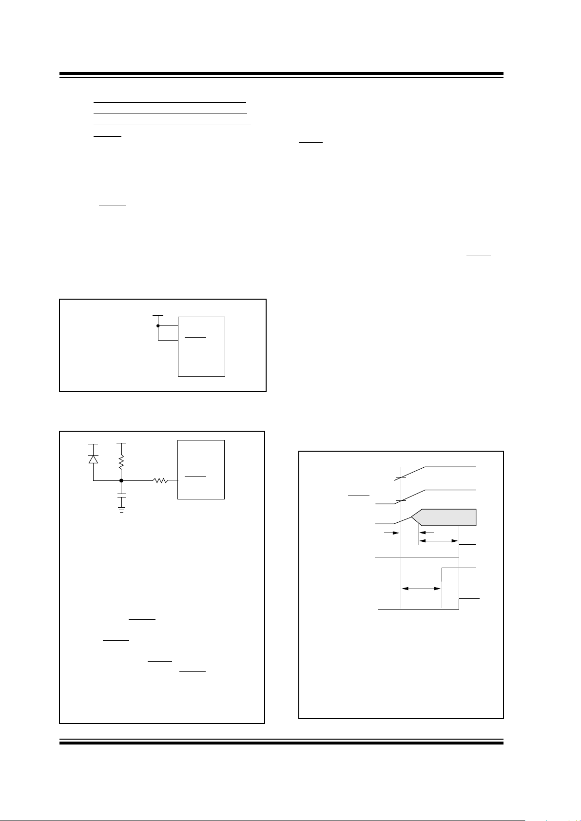
4.1.2.1 OSCILLATOR / RESONATOR START-UP
As the device voltage increases from Vss , the oscillator
will start its oscillations. The time required for the oscillator to start oscillating depends on many factors.
These include:
• Crystal / resonator frequency
• Capacitor values used (C1 and C2)
• Device V
DD rise time.
• System temperature
• Series resistor value (and type) if used
• Oscillator mode selection of device (which selects
the gain of the internal oscillator inverter)
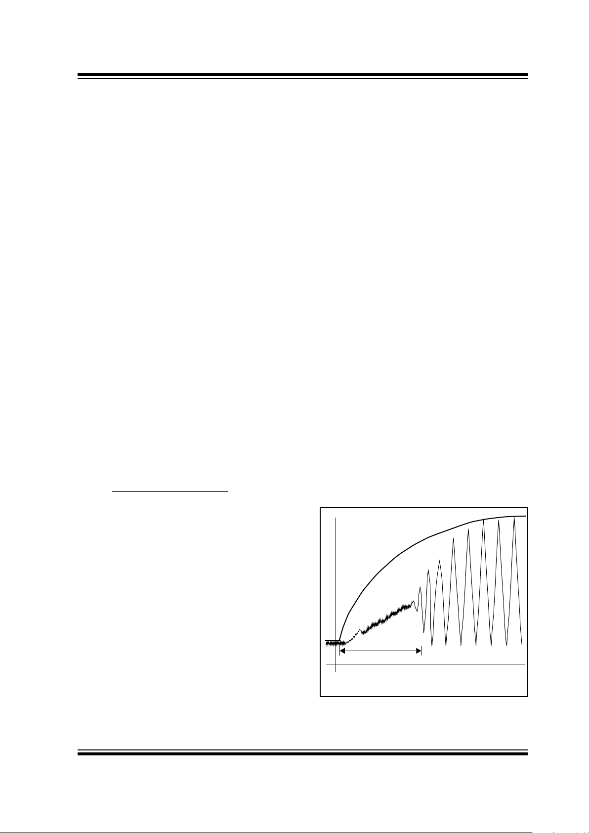
Figure 4-1 shows an example of a typical oscillator /
resonator start-up. The peak-to-peak voltage of the
oscillator waveform can be quite low (less than 50% of
device V
DD) when the waveform is centered at VDD/2
(refer to parameter number D033 and D043 in the electrical specification section).
FIGURE 4-1: OSCILLATOR / RESONATOR
START-UP
CHARACTERISTICS
VDD
Crystal Start-up Time
Time
PIC17C75X
DS30264A-page 16 Preliminary 1997 Microchip Technology Inc.
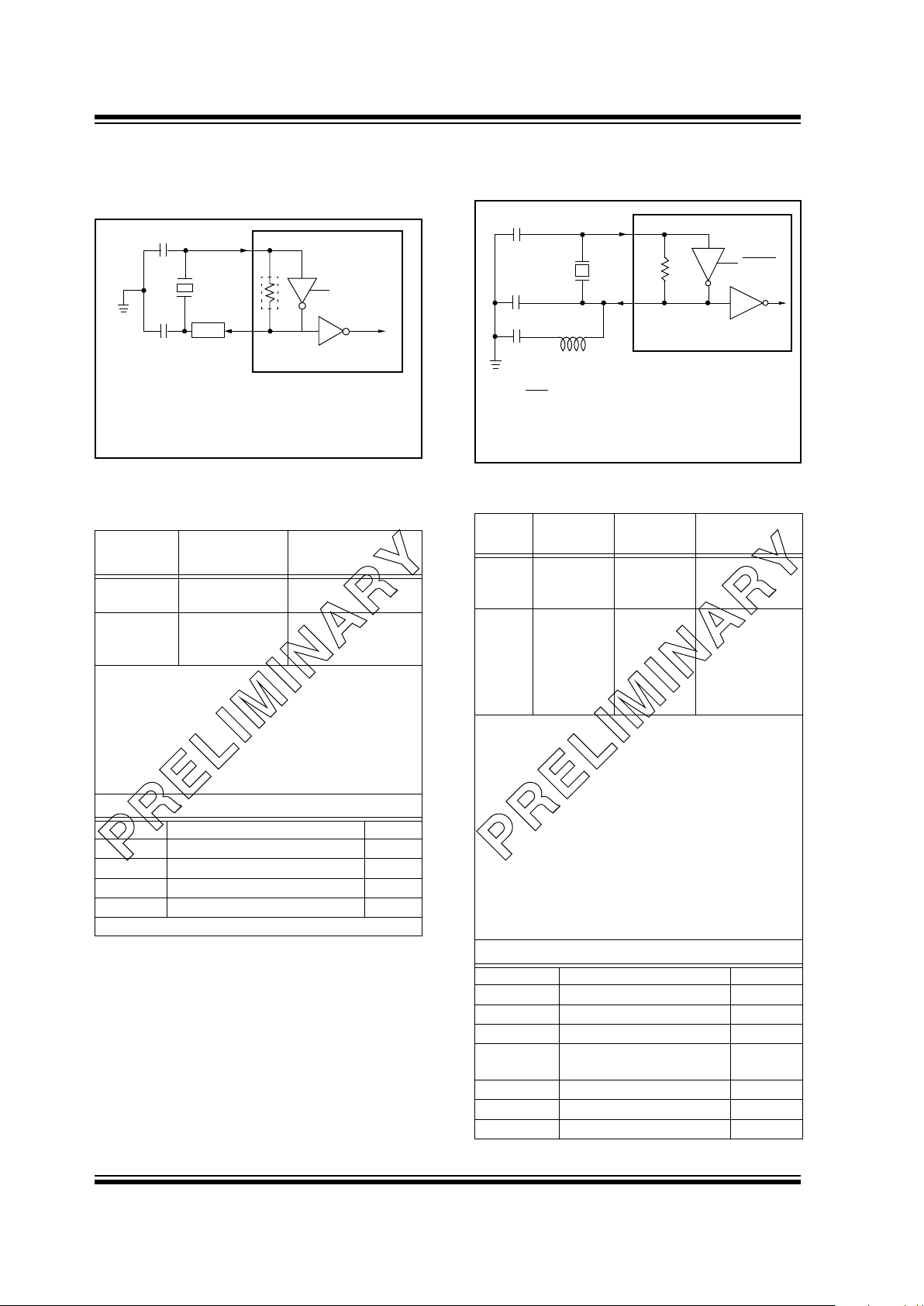
FIGURE 4-2: CRYSTAL OR CERAMIC
RESONATOR OPERATION (XT
OR LF OSC CONFIGURATION)
TABLE 4-1: CAPACITOR SELECTION
FOR CERAMIC
RESONATORS
Oscillator
Type
Resonator
Frequency
Capacitor Range
C1 = C2
(1)
LF 455 kHz
2.0 MHz
15 - 68 pF
10 - 33 pF
XT 4.0 MHz
8.0 MHz
16.0 MHz
22 - 68 pF
33 - 100 pF
33 - 100 pF
Higher capacitance increases the stability of the oscillator
but also increases the start-up time. These values are for
design guidance only. Since each resonator has its own
characteristics, the user should consult the resonator manufacturer for appropriate values of external components.
Note 1: These values include all board capaci-
tances on this pin. Actual capacitor value
depends on board capacitance
Resonators Used:
455 kHz Panasonic EFO-A455K04B ± 0.3%
2.0 MHz Murata Erie CSA2.00MG ± 0.5%
4.0 MHz Murata Erie CSA4.00MG ± 0.5%
8.0 MHz Murata Erie CSA8.00MT ± 0.5%
16.0 MHz Murata Erie CSA16.00MX ± 0.5%
Resonators used did not have built-in capacitors.
See Table 4-1 and Table 4-2 for recommended values of
C1 and C2.
Note 1: A series resistor (Rs) may be required for
AT strip cut crystals.
C1
C2
XTAL
OSC2
Note1
OSC1
RF
SLEEP
PIC17CXXX
To internal
logic
FIGURE 4-3: CRYSTAL OPERATION,
OVERTONE CRYSTALS (XT
OSC CONFIGURATION)
TABLE 4-2: CAPACITOR SELECTION FOR
CRYSTAL OSCILLATOR
Osc
Type
Freq
C1
(3)
C2
(3)
LF 32 kHz
(1)
1 MHz
2 MHz
100-150 pF
10-33 pF
10-33 pF
100-150 pF
10-33 pF
10-33 pF
XT 2 MHz
4 MHz
8 MHz
(2)
16 MHz
25 MHz
32 MHz
(3)
47-100 pF
15-68 pF
15-47 pF
TBD
15-47 pF
10
47-100 pF
15-68 pF
15-47 pF
TBD
15-47 pF
10
Higher capacitance increases the stability of the oscillator
but also increases the start-up time and the oscillator current. These values are for design guidance only. RS may be
required in XT mode to avoid overdriving the crystals with
low drive level specification. Since each crystal has its own
characteristics, the user should consult the crystal manufacturer for appropriate values for external components.
Note 1: For VDD > 4.5V, C1 = C2 ≈ 30 pF is recom-
mended.
2: R
S of 330Ω is required for a capacitor com-
bination of 15/15 pF.
3: These values include all board capaci-
tances on this pin. Actual capacitor value
depends on board capacitance
Crystals Used:
32.768 kHz Epson C-001R32.768K-A ± 20 PPM
1.0 MHz ECS-10-13-1 ± 50 PPM
2.0 MHz ECS-20-20-1 ± 50 PPM
4.0 MHz ECS-40-20-1 ± 50 PPM
8.0 MHz ECS ECS-80-S-4
ECS-80-18-1
± 50 PPM
16.0 MHz ECS-160-20-1 TBD
25 MHz CTS CTS25M ± 50 PPM
32 MHz CRYSTEK HF-2 ± 50 PPM
C1
C2
0.1 µF
SLEEP
OSC2
OSC1
PIC17CXXX
To filter the fundamental frequency
1
LC2
=
(2πf)
2
Where f = tank circuit resonant frequency. This should be
midway between the fundamental and the 3rd overtone
frequencies of the crystal.
1997 Microchip Technology Inc. Preliminary DS30264A-page 17
PIC17C75X
4.1.3 EXTERNAL CLOCK OSCILLATOR
In the EC oscillator mode, the OSC1 input can be
driven by CMOS drivers. In this mode, the
OSC1/CLKIN pin is hi-impedance and the OSC2/CLKOUT pin is the CLKOUT output (4 T
OSC).
FIGURE 4-4: EXTERNAL CLOCK INPUT
OPERATION (EC OSC
CONFIGURATION)
Clock from
ext. system
OSC1
OSC2
PIC17CXXX
CLKOUT
(F
OSC/4)
4.1.4 EXTERNAL CRYSTAL OSCILLATOR
CIRCUIT
Either a prepackaged oscillator can be used or a simple
oscillator circuit with TTL gates can be built. Prepackaged oscillators provide a wide operating range and
better stability. A well-designed crystal oscillator will
provide good performance with TTL gates. Two types
of crystal oscillator circuits can be used: one with series
resonance, or one with parallel resonance.
Figure 4-5 shows implementation of a parallel resonant
oscillator circuit. The circuit is designed to use the fundamental frequency of the crystal. The 74AS04 inverter
performs the 180-degree phase shift that a parallel
oscillator requires. The 4.7 kΩ resistor provides the
negative feedback for stability. The 10 kΩ potentiometer biases the 74AS04 in the linear region. This could
be used for external oscillator designs.
FIGURE 4-5: EXTERNAL PARALLEL
RESONANT CRYSTAL
OSCILLATOR CIRCUIT
Figure 4-6 shows a series resonant oscillator circuit.
This circuit is also designed to use the fundamental frequency of the crystal. The inverter performs a
180-degree phase shift in a series resonant oscillator
circuit. The 330 kΩ resistors provide the negative feedback to bias the inverters in their linear region.
FIGURE 4-6: EXTERNAL SERIES
RESONANT CRYSTAL
OSCILLATOR CIRCUIT
20 pF
+5V
20 pF
10k
4.7k
10k
74AS04
XTAL
10k
74AS04
PIC17CXXX
OSC1
To Other
Devices
330 kΩ
74AS04
74AS04
PIC17CXXX
OSC1
To Other
Devices
XTAL
330 kΩ
74AS04
0.1 µF
PIC17C75X
DS30264A-page 18 Preliminary 1997 Microchip Technology Inc.
4.1.5 RC OSCILLATOR
For timing insensitive applications, the RC device
option offers additional cost savings. RC oscillator frequency is a function of the supply voltage, the resistor
(Rext) and capacitor (Cext) values, and the operating
temperature. In addition to this, oscillator frequency will
vary from unit to unit due to normal process parameter
variation. Furthermore, the difference in lead frame
capacitance between package types will also affect
oscillation frequency, especially for low Cext values.
The user also needs to take into account variation due
to tolerance of external R and C components used.
Figure 4-7 shows how the R/C combination is connected to the PIC17CXXX. For Rext values below
2.2 kΩ, the oscillator operation may become unstable,
or stop completely. For very high Rext values (e.g.
1 MΩ), the oscillator becomes sensitive to noise,
humidity and leakage. Thus, we recommend to keep
Rext between 3 kΩ and 100 kΩ.
Although the oscillator will operate with no external
capacitor (Cext = 0 pF), we recommend using values
above 20 pF for noise and stability reasons. With little
or no external capacitance, oscillation frequency can
vary dramatically due to changes in external capacitances, such as PCB trace capacitance or package
lead frame capacitance.
See Section 21.0 for RC frequency variation from part
to part due to normal process variation. The variation
is larger for larger R (since leakage current variation
will affect RC frequency more for large R) and for
smaller C (since variation of input capacitance will
affect RC frequency more).
See Section 21.0 for variation of oscillator frequency
due to V
DD for given Rext/Cext values as well as fre-
quency variation due to operating temperature for
given R, C, and V
DD values.
The oscillator frequency, divided by 4, is available on
the OSC2/CLKOUT pin, and can be used for test purposes or to synchronize other logic (see Figure 4-8 for
waveform).
FIGURE 4-7: RC OSCILLATOR MODE
VDD
Rext
Cext
V
SS
OSC1
Internal
clock
OSC2/CLKOUT
Fosc/4
PIC17CXXX
4.1.5.1 RC START-UP
As the device voltage increases, the RC will immedi-
ately start its oscillations once the pin voltage levels
meet the input threshold specifications (parameter
number D032 and D042 in the electrical specification
section). The time required for the RC to start oscillating depends on many factors. These include:
• Resistor value used
• Capacitor value used
• Device V
DD rise time
• System temperature
1997 Microchip Technology Inc. Preliminary DS30264A-page 19
PIC17C75X
4.2 Clocking Scheme/Instruction Cycle
The clock input (from OSC1) is internally divided by
four to generate four non-overlapping quadrature
clocks, namely Q1, Q2, Q3, and Q4. Internally, the program counter (PC) is incremented every Q1, and the
instruction is fetched from the program memory and
latched into the instruction register in Q4. The instruction is decoded and executed during the following Q1
through Q4. The clocks and instruction execution flow
are shown in Figure 4-8.
4.3 Instruction Flow/Pipelining
An “Instruction Cycle” consists of four Q cycles (Q1,
Q2, Q3, and Q4). The instruction fetch and ex ecute are
pipelined such that fetch takes one instruction cycle
while decode and execute takes another instruction
cycle. However, due to the pipelining, each instruction
effectively executes in one cycle. If an instruction
causes the program counter to change (e.g. GOTO)
then two cycles are required to complete the instruction
(Example 4-1).
A fetch cycle begins with the program counter incrementing in Q1.
In the execution cycle, the f etched instruction is latched
into the “Instruction Register (IR)” in cycle Q1. This
instruction is then decoded and executed during the
Q2, Q3, and Q4 cycles. Data memory is read during Q2
(operand read) and written during Q4 (destination
write).
FIGURE 4-8: CLOCK/INSTRUCTION CYCLE
EXAMPLE 4-1: INSTRUCTION PIPELINE FLOW
Q1
Q2 Q3 Q4
Q1
Q2 Q3 Q4
Q1
Q2 Q3 Q4
OSC1
Q1
Q2
Q3
Q4
PC
OSC2/CLKOUT
(RC mode)
PC PC+1 PC+2
Fetch INST (PC)
Execute INST (PC-1) Fetch INST (PC+1)
Execute INST (PC) Fetch INST (PC+2)
Execute INST (PC+1)
Internal
phase
clock
All instructions are single cycle, except for any program branches. These take two cycles since the fetch
instruction is “flushed” from the pipeline while the new instruction is being fetched and then executed.
Tcy0 Tcy1 Tcy2 Tcy3 Tcy4 Tcy5
1. MOVLW 55h
Fetch 1 Execute 1
2. MOVWF PORTB
Fetch 2 Execute 2
3. CALL SUB_1
Fetch 3 Execute 3
4. BSF PORTA, BIT3 (Forced NOP)
Fetch 4 Flush
5. Instruction @ address SUB_1
Fetch SUB_1 Execute SUB_1

PIC17C75X
DS30264A-page 20 Preliminary 1997 Microchip Technology Inc.
NOTES:
1997 Microchip Technology Inc. Preliminary DS30264A-page 21
PIC17C75X
5.0 RESET
The PIC17CXXX differentiates between various kinds
of reset:
• Power-on Reset (POR)
• MCLR
reset during normal operation
• Brown-out Reset
• WDT Reset (normal operation)
Some registers are not affected in any reset condition,
their status is unknown on POR and unchanged in any
other reset. Most other registers are forced to a “reset
state” on Power-on Reset (POR), Brown-out Reset
(BOR), on MCLR
or WDT Reset and on MCLR reset
during SLEEP. A WDT Reset during SLEEP, is viewed
as the resumption of normal operation. The T
O and PD
bits are set or cleared differently in different reset situations as indicated in Table 5-3. These bits are used in
software to determine the nature of the reset. See
Table 5-4 for a full description of reset states of all registers.
A simplified block diagram of the on-chip reset circuit is
shown in Figure 5-1.
Note: While the device is in a reset state, the
internal phase clock is held in the Q1 state.
Any processor mode that allows external
execution will force the RE0/ALE pin as a
low output and the RE1/OE
and RE2/WR
pins as high outputs.
FIGURE 5-1: SIMPLIFIED BLOCK DIAGRAM OF ON-CHIP RESET CIRCUIT
S
R
Q
External
Reset
MCLR
VDD
OSC1
WDT
Module
V
DD rise
detect
OST/PWRT
On-chip
RC OSC†
WDT
Time_Out
Power_On_Reset
OST
10-bit Ripple counter
PWRT
Chip_Reset
10-bit Ripple counter
Power_Up
(Enable the PWRT timer
only during Power_Up)
(Power_Up) + (Wake_Up) (XT + LF)
(Enable the OST if it is Power_Up or Wake_Up
from SLEEP and OSC type is XT or LF)
Reset
Enable OST
Enable PWRT
† This RC oscillator is shared with the WDT
when not in a power-up sequence.
BOR
Module
Brown-out
Reset
PIC17C75X
DS30264A-page 22 Preliminary 1997 Microchip Technology Inc.
5.1 Power-on Reset (POR), Power-up
Timer (PWRT), Oscillator Start-up
Timer (OST), and Brown-out Reset
(BOR)
5.1.1 POWER-ON RESET (POR)
The Power-on Reset circuit holds the device in reset
until V
DD is above the trip point (in the range of 1.4V -
2.3V). The devices produce an internal reset for both
rising and falling V
DD. To take advantage of the POR,
just tie the MCLR/
VPP pin directly (or through a resistor)
to V
DD. This will eliminate external RC components
usually needed to create Power-on Reset. A minimum
rise time for V
DD is required. See Electrical Specifica-
tions for details.
Figure 5-2 and Figure 5-3 show two possible POR cir-
cuits.
FIGURE 5-2: USING ON-CHIP POR
FIGURE 5-3: EXTERNAL POWER-ON
RESET CIRCUIT (FOR SLOW
V
DD POWER-UP)
VDD
MCLR
PIC17CXXX
VDD
Note 1: An external Power-on Reset circuit is
required only if V
DD power-up time is too
slow. The diode D helps discharge the
capacitor quickly when V
DD powers
down.
2: R < 40 kΩ is recommended to ensure
that the voltage drop across R does not
exceed 0.2V (max. leakage current spec.
on the MCLR/
VPP pin is 5 µA). A larger
voltage drop will degrade V
IH level on the
MCLR/
VPP pin.
3: R1 = 100Ω to 1 kΩ will limit any current
flowing into MCLR
from external capaci-
tor C in the event of MCLR/
VPP pin
breakdown due to Electrostatic Discharge (ESD) or Electrical Overstress
(EOS).
C
R1
R
D
V
DD
MCLR
PIC17CXXX
VDD
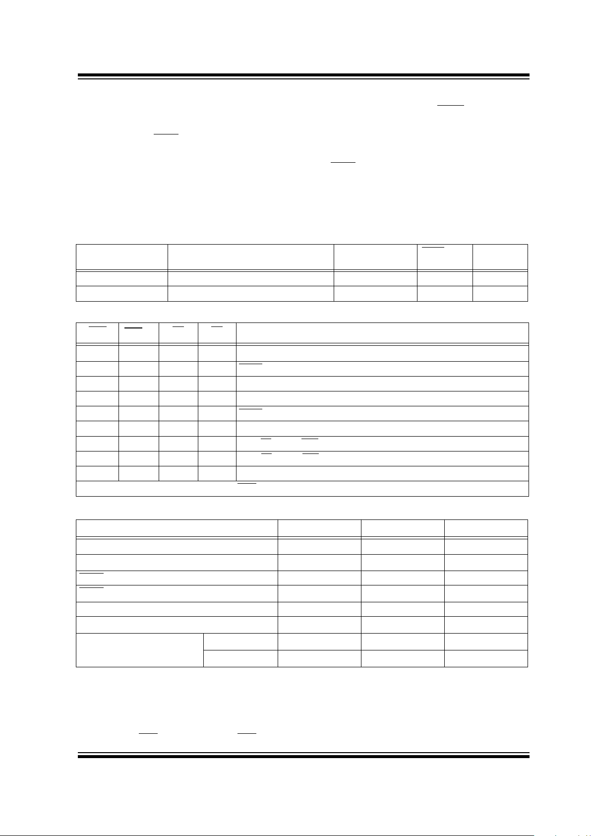
5.1.2 P O WER-UP TIMER (PWRT)
The Power-up Timer provides a fixed 96 ms time-out
(nominal) on power-up. This occurs from the rising
edge of the POR signal and after the first rising edge of
MCLR
(detected high). The Power-up Timer operates
on an internal RC oscillator. The chip is kept in RESET
as long as the PWRT is active. In most cases the
PWRT delay allows V
DD to rise to an acceptable level.
The power-up time delay will vary from chip to chip and
with V
DD and temperature. See DC parameters for
details.
5.1.3 OSCILLATOR START-UP TIMER (OST)
The Oscillator Start-up Timer (OST) provides a 1024
oscillator cycle (1024T
OSC) delay after MCLR is
detected high or a wake-up from SLEEP event occurs.
The OST time-out is invoked only for XT and LF oscil-
lator modes on a Power-on Reset or a Wake-up from
SLEEP.
The OST counts the oscillator pulses on the
OSC1/CLKIN pin. The counter only starts incrementing
after the amplitude of the signal reaches the oscillator
input thresholds. This delay allows the crystal oscillator
or resonator to stabilize before the device exits reset.
The length of the time-out is a function of the crystal/resonator frequency.
Figure 5-4 shows the operation of the OST circuit. In
this figure the oscillator is of such a low frequency that
OST time out occurs after the power-up timer time-out.
FIGURE 5-4: OSCILLATOR START-UP
TIME
VDD
MCLR
OSC2
OST TIME_OUT
PWRT TIME_OUT
INTERNAL RESET
T
OSC1
T
OST
TPWRT
POR or BOR Trip Point
This figure shows in greater detail the timings involved
with the oscillator start-up timer. In this example the low
frequency crystal start-up time is larger than power-up
time (T
PWRT).
Tosc1 = time for the crystal oscillator to react to an oscillation level detectable by the Oscillator Start-up Timer
(ost).
TOST = 1024TOSC.
1997 Microchip Technology Inc. Preliminary DS30264A-page 23
PIC17C75X
5.1.4 TIME-OUT SEQUENCE
On power-up the time-out sequence is as follows: First
the internal POR signal goes high when the POR trip
point is reached. If MCLR
is high, then both the OST
and PWRT timers start. In general the PWRT time-out
is longer, except with low frequency crystals/resonators. The total time-out also varies based on oscillator
configuration. Table 5-1 shows the times that are associated with the oscillator configuration. Figure 5-5 and
Figure 5-6 display these time-out sequences.
If the device voltage is not within electrical specification
at the end of a time-out, the MCLR/
VPP pin must be
held low until the voltage is within the device specification. The use of an external RC delay is sufficient for
many of these applications.
The time-out sequence begins from the first rising edge
of MCLR
.
Table 5-3 shows the reset conditions for some special
registers, while Table 5-4 shows the initialization conditions for all the registers.
TABLE 5-1: TIME-OUT IN VARIOUS SITUATIONS
TABLE 5-2: STATUS BITS AND THEIR SIGNIFICANCE
TABLE 5-3: RESET CONDITION FOR THE PROGRAM COUNTER AND THE CPUSTA REGISTER
Oscillator
Configuration
Power-up Wake up from
SLEEP
MCLR Reset BOR
XT, LF Greater of: 96 ms or 1024TOSC 1024TOSC ——
EC, RC Greater of: 96 ms or 1024T
OSC ———
POR
BOR
(1)
TO PD
Event
0011
Power-on Reset
1110
MCLR Reset during SLEEP or interrupt wake-up from SLEEP
1101
WDT Reset during normal operation
1100
WDT W ake-up during SLEEP
1111
MCLR Reset during normal operation
10xx
Brown-out Reset
000x
Illegal, TO is set on POR
00x0
Illegal, PD is set on POR
xx11
CLRWDT instruction executed
Note 1: When BOR is enabled, else the BOR status bit is unknown
Event PCH:PCL CPUSTA
(4)
OST Active
Power-on Reset 0000h --11 1100 Yes
Brown-out Reset 0000h --11 1101 No
MCLR
Reset during normal operation 0000h --11 1111 No
MCLR
Reset during SLEEP 0000h --11 1011
Yes
(2)
WDT Reset during normal operation 0000h --11 0111 No
WDT Wake-up during SLEEP
(3)
0000h --11 0011
Yes
(2)
Interrupt wake-up from SLEEP GLINTD is set PC + 1 --11 1011
Yes
(2)
GLINTD is clear
PC + 1
(1)
--10 1011
Yes
(2)
Legend: u = unchanged, x = unknown, - = unimplemented read as '0'.
Note 1: On wake-up, this instruction is executed. The instruction at the appropriate interrupt vector is fetched and
then executed.
2: The OST is only active when the Oscillator is configured for XT or LF modes.
3: The Program Counter = 0, that is, the device branches to the reset vector. This is different from the
mid-range devices.
4: When BOR
is enabled, else the BOR status bit is unknown.

PIC17C75X
DS30264A-page 24 Preliminary 1997 Microchip Technology Inc.
In Figure 5-5, Figure 5-6 and Figure 5-7, TPWRT >
T
OST, as would be the case in higher frequency crys-
tals. For lower frequency crystals, (i.e., 32 kHz) T
OST
would be greater.
FIGURE 5-5: TIME-OUT SEQUENCE ON POWER-UP (MCLR TIED TO VDD)
FIGURE 5-6: TIME-OUT SEQUENCE ON POWER-UP (MCLR
NOT TIED TO VDD)
FIGURE 5-7: SLOW RISE TIME (MCLR
TIED TO VDD)
TPWRT
TOST
VDD
MCLR
INTERNAL POR
PWRT TIME-OUT
OST TIME-OUT
INTERNAL RESET
TPWRT
TOST
VDD
MCLR
INTERNAL POR
PWRT TIME-OUT
OST TIME-OUT
INTERNAL RESET
VDD
MCLR
INTERNAL POR
PWR
T TIME-OUT
OST TIME-OUT
INTERNAL RESET
0V
1V
5V
TPWRT
TOST
Minimum VDD operating voltage
1997 Microchip Technology Inc. Preliminary DS30264A-page 25
PIC17C75X
TABLE 5-4: INITIALIZATION CONDITIONS FOR SPECIAL FUNCTION REGISTERS
Register Address
Power-on Reset
Brown-out Reset
MCLR
Reset
WDT Reset
Wake-up from SLEEP
through interrupt
Unbanked
INDF0 00h N.A. N.A. N.A.
FSR0 01h xxxx xxxx uuuu uuuu uuuu uuuu
PCL 02h 0000h 0000h
PC + 1
(2)
PCLATH 03h 0000 0000 0000 0000 uuuu uuuu
ALUSTA 04h 1111 xxxx 1111 uuuu 1111 uuuu
T0STA 05h 0000 000- 0000 000- 0000 000-
CPUSTA
(3)
06h
--11 1100
(4)
--11 qquu
(4)
--uu qquu
(4)
INTSTA 07h 0000 0000 0000 0000
uuuu uuuu
(1)
INDF1 08h N.A. N.A. N.A.
FSR1 09h xxxx xxxx uuuu uuuu uuuu uuuu
WREG 0Ah xxxx xxxx uuuu uuuu uuuu uuuu
TMR0L 0Bh xxxx xxxx uuuu uuuu uuuu uuuu
TMR0H 0Ch xxxx xxxx uuuu uuuu uuuu uuuu
TBLPTRL 0Dh 0000 0000 0000 0000 uuuu uuuu
TBLPTRH 0Eh 0000 0000 0000 0000 uuuu uuuu
BSR 0Fh 0000 0000 0000 0000 uuuu uuuu
Bank 0
PORTA 10h 0-xx xxxx 0-uu uuuu u-uu uuuu
DDRB 11h 1111 1111 1111 1111 uuuu uuuu
PORTB 12h xxxx xxxx uuuu uuuu uuuu uuuu
RCSTA1 13h 0000 -00x 0000 -00u uuuu -uuu
RCREG1 14h xxxx xxxx uuuu uuuu uuuu uuuu
TXSTA1 15h 0000 --1x 0000 --1u uuuu --uu
TXREG1 16h xxxx xxxx uuuu uuuu uuuu uuuu
SPBRG1 17h xxxx xxxx uuuu uuuu uuuu uuuu
Bank 1
DDRC 10h 1111 1111 1111 1111 uuuu uuuu
PORTC 11h xxxx xxxx uuuu uuuu uuuu uuuu
DDRD 12h 1111 1111 1111 1111 uuuu uuuu
PORTD 13h xxxx xxxx uuuu uuuu uuuu uuuu
DDRE 14h ---- 1111 ---- 1111 ---- uuuu
PORTE 15h ---- xxxx ---- uuuu ---- uuuu
PIR1 16h x000 0010 u000 0010
uuuu uuuu
(1)
PIE1 17h 0000 0000 0000 0000 uuuu uuuu
Legend: u = unchanged, x = unknown, - = unimplemented read as '0', q = value depends on condition.
Note 1: One or more bits in INTSTA, PIR1, PIR2 will be affected (to cause wake-up).
2: When the wake-up is due to an interrupt and the GLINTD bit is cleared, the PC is loaded with the interrupt
vector.
3: See Table 5-3 for reset value of specific condition.
4: If Brown-out is enabled, else the BOR
bit is unknown.
PIC17C75X
DS30264A-page 26 Preliminary 1997 Microchip Technology Inc.
Bank 2
TMR1 10h xxxx xxxx uuuu uuuu uuuu uuuu
TMR2 11h xxxx xxxx uuuu uuuu uuuu uuuu
TMR3L 12h xxxx xxxx uuuu uuuu uuuu uuuu
TMR3H 13h xxxx xxxx uuuu uuuu uuuu uuuu
PR1 14h xxxx xxxx uuuu uuuu uuuu uuuu
PR2 15h xxxx xxxx uuuu uuuu uuuu uuuu
PR3/CA1L 16h xxxx xxxx uuuu uuuu uuuu uuuu
PR3/CA1H 17h xxxx xxxx uuuu uuuu uuuu uuuu
Bank 3
PW1DCL 10h xx-- ---- uu-- ---- uu-- ----
PW2DCL 11h xx0- ---- uu0- ---- uuu- ----
PW1DCH 12h xxxx xxxx uuuu uuuu uuuu uuuu
PW2DCH 13h xxxx xxxx uuuu uuuu uuuu uuuu
CA2L 14h xxxx xxxx uuuu uuuu uuuu uuuu
CA2H 15h xxxx xxxx uuuu uuuu uuuu uuuu
TCON1 16h 0000 0000 0000 0000 uuuu uuuu
TCON2 17h 0000 0000 0000 0000 uuuu uuuu
Bank 4
PIR2 10h 000- 0010 000- 0010
uuu- uuuu
(1)
PIE2 11h 000- 0000 000- 0000 uuu- uuuu
Unimplemented
12h ---- ---- ---- ---- ---- ---RCSTA2 13h 0000 -00x 0000 -00u uuuu -uuu
RCREG2 14h xxxx xxxx uuuu uuuu uuuu uuuu
TXSTA2 15h 0000 --1x 0000 --1u uuuu --uu
TXREG2 16h xxxx xxxx uuuu uuuu uuuu uuuu
SPBRG2 17h xxxx xxxx uuuu uuuu uuuu uuuu
Bank 5
DDRF 10h 1111 1111 1111 1111 uuuu uuuu
PORTF 11h xxxx xxxx uuuu uuuu uuuu uuuu
DDRG 12h 1111 1111 1111 1111 uuuu uuuu
PORTG 13h xxxx xxxx uuuu uuuu uuuu uuuu
ADCON0 14h 0000 -0-0 0000 -0-0 uuuu uuuu
ADCON1 15h 000- 0000 000- 0000 uuuu uuuu
ADRESL 16h xxxx xxxx xxxx xxxx uuuu uuuu
ADRESH 17h xxxx xxxx xxxx xxxx uuuu uuuu
TABLE 5-4: INITIALIZATION CONDITIONS FOR SPECIAL FUNCTION REGISTERS (Cont.’d)
Register Address
Power-on Reset
Brown-out Reset
MCLR
Reset
WDT Reset
Wake-up from SLEEP
through interrupt
Legend: u = unchanged, x = unknown, - = unimplemented read as '0', q = value depends on condition.
Note 1: One or more bits in INTSTA, PIR1, PIR2 will be affected (to cause wake-up).
2: When the wake-up is due to an interrupt and the GLINTD bit is cleared, the PC is loaded with the interrupt
vector.
3: See Table 5-3 for reset value of specific condition.
4: If Brown-out is enabled, else the BOR
bit is unknown.
1997 Microchip Technology Inc. Preliminary DS30264A-page 27
PIC17C75X
Bank 6
SSPADD 10h 0000 0000 0000 0000 uuuu uuuu
SSPCON1 11h 0000 0000 0000 0000 uuuu uuuu
SSPCON2 12h 0000 0000 0000 0000 uuuu uuuu
SSPSTAT 13h 0000 0000 0000 0000 uuuu uuuu
SSPBUF 14h xxxx xxxx uuuu uuuu uuuu uuuu
Unimplemented
15h ---- ---- ---- ---- ---- ----
Unimplemented
16h ---- ---- ---- ---- ---- ----
Unimplemented
17h ---- ---- ---- ---- ---- ----
Bank 7
PW3DCL 10h xxx- ---- uuu- ---- uuu- ----
PW3DCH 11h xxxx xxxx uuuu uuuu uuuu uuuu
CA3L 12h xxxx xxxx uuuu uuuu uuuu uuuu
CA3H 13h xxxx xxxx uuuu uuuu uuuu uuuu
CA4L 14h xxxx xxxx uuuu uuuu uuuu uuuu
CA4H 15h xxxx xxxx uuuu uuuu uuuu uuuu
TCON3 16h -000 0000 -000 0000 -uuu uuuu
Unimplemented
17h ---- ---- ---- ---- ---- ----
Unbanked
PRODL 18h xxxx xxxx uuuu uuuu uuuu uuuu
PRODH 19h xxxx xxxx uuuu uuuu uuuu uuuu
TABLE 5-4: INITIALIZATION CONDITIONS FOR SPECIAL FUNCTION REGISTERS (Cont.’d)
Register Address
Power-on Reset
Brown-out Reset
MCLR
Reset
WDT Reset
Wake-up from SLEEP
through interrupt
Legend: u = unchanged, x = unknown, - = unimplemented read as '0', q = value depends on condition.
Note 1: One or more bits in INTSTA, PIR1, PIR2 will be affected (to cause wake-up).
2: When the wake-up is due to an interrupt and the GLINTD bit is cleared, the PC is loaded with the interrupt
vector.
3: See Table 5-3 for reset value of specific condition.
4: If Brown-out is enabled, else the BOR
bit is unknown.
PIC17C75X
DS30264A-page 28 Preliminary 1997 Microchip Technology Inc.
5.1.5 BROWN-OUT RESET (BOR)
PIC17C75X devices have an on-chip Brown-out Reset
circuitry. This circuitry places the device into a reset
when the device voltage f alls below a trip point (BV
DD).
This ensures that the device does not continue program execution outside the v alid oper ation range of the
device. Brown-out resets are typically used in AC line
applications or large battery applications where large
loads may be switched in (such as automotive).
A configuration bit, BODEN, can disable (if clear/programmed) or enable (if set) the Brown-out Reset circuitry. If V
DD falls below BVDD (Typically 4.0V,
parameter D005 in electrical specification section), for
greater than parameter D035, the brown-out situation
will reset the chip. A reset is not guaranteed to occur if
V
DD falls below BVDD for less than parameter D035.
The chip will remain in Brown-out Reset until V
DD rises
above BV
DD. The Power-up Timer will now be invoked
and will keep the chip in reset an additional 96 ms. If
V
DD drops below BVDD while the Power-up Timer is
running, the chip will go back into a Brown-out Reset
and the Power-up Timer will be initialized. Once V
DD
rises above BVDD, the Power-up Timer will execute a
96 ms time delay. Figure 5-10 shows typical Brown-out
situations.
In some applications the Brown-out reset trip point of
the device may not be at the desired level. Figure 5-8
and Figure 5-9 are two examples of external circuitry
that may be implemented. Each needs to be evaluated
to determine if they match the requirements of the
application.
Note: Before using the on-chip brown-out for a
voltage supervisory function, please
review the electrical specifications to
ensure that they meet your requirements.
FIGURE 5-8: EXTERNAL BROWN-OUT
PROTECTION CIRCUIT 1
FIGURE 5-9: EXTERNAL BROWN-OUT
PROTECTION CIRCUIT 2
VDD
33k
10k
40 kΩ
V
DD
MCLR
PIC17CXXX
This circuit will activate reset when VDD goes below
(Vz + 0.7V) where Vz = Zener voltage.
This brown-out circuit is less expensive, albeit less
accurate. Transistor Q1 turns off when VDD is below a
certain level such that:
VDD •
R1
R1 + R2
= 0.7V
R2
40 kΩ
VDD
MCLR
PIC17CXXX
R1
Q1
V
DD
FIGURE 5-10: BROWN-OUT SITUATIONS
96 ms
BV
DD Max.
BV
DD Min.
V
DD
Internal
Reset
BVDD Max.
BV
DD Min.
V
DD
Internal
Reset
96 ms
< 96 ms
96 ms
BVDD Max.
BV
DD Min.
V
DD
Internal
Reset
1997 Microchip Technology Inc. Preliminary DS30264A-page 29
PIC17C75X
6.0 INTERRUPTS
The PIC17C75X devices have 18 sources of interrupt:
• External interrupt from the RA0/INT pin
• Change on RB7:RB0 pins
• TMR0 Overflow
• TMR1 Overflow
• TMR2 Overflow
• TMR3 Overflow
• USART1 Transmit buffer empty
• USART1 Receive buffer full
• USART2 Transmit buffer empty
• USART2 Receive buffer full
• SSP Interrupt
• SSP I
2
C bus collision interrupt
• A/D conversion complete
• Capture1
• Capture2
• Capture3
• Capture4
• T0CKI edge occurred
There are six registers used in the control and status of
interrupts. These are:
• CPUST A
• INTST A
• PIE1
• PIR1
• PIE2
• PIR2
The CPUSTA register contains the GLINTD bit. This is
the Global Interrupt Disable bit. When this bit is set, all
interrupts are disabled. This bit is part of the controller
core functionality and is described in the Memory Organization section.
When an interrupt is responded to, the GLINTD bit is
automatically set to disable any further interrupts, the
return address is pushed onto the stack and the PC is
loaded with the interrupt vector address. There are four
interrupt vectors. Each vector address is for a specific
interrupt source (except the peripheral interrupts which
all vector to the same address). These sources are:
• External interrupt from the RA0/INT pin
• TMR0 Overflow
• T0CKI edge occurred
• Any peripheral interrupt
When program execution vectors to one of these inter-
rupt vector addresses (except for the peripheral interrupts), the interrupt flag bit is automatically cleared.
Vectoring to the peripheral interrupt vector address
does not automatically clear the source of the interrupt.
In the peripheral interrupt service routine, the source(s)
of the interrupt can be determined by testing the interrupt flag bits. The interrupt flag bit(s) must be cleared in
software before re-enabling interrupts to avoid infinite
interrupt requests.
When an interrupt condition is met, that individual interrupt flag bit will be set regardless of the status of its corresponding mask bit or the GLINTD bit.
For external interrupt events, there will be an interrupt
latency. For two cycle instructions, the latency could be
one instruction cycle longer.
The “return from interrupt” instruction, RETFIE, can be
used to mark the end of the interrupt service routine.
When this instruction is executed, the stack is
“POPed”, and the GLINTD bit is cleared (to re-enable
interrupts).
FIGURE 6-1: INTERRUPT LOGIC
RBIF
RBIE
TMR3IF
TMR3IE
TMR2IF
TMR2IE
TMR1IF
TMR1IE
CA2IF
CA2IE
CA1IF
CA1IE
TX1IF
TX1IE
RC1IF
RC1IE
T0IF
T0IE
INTF
INTE
T0CKIF
T0CKIE
GLINTD (CPUSTA<4>)
PEIE
Wake-up (If in SLEEP mode)
or terminate long write
Interrupt to CPU
PEIF
SSPIF
SSPIE
BCLIF
BCLIE
ADIF
ADIE
CA4IF
CA4IE
CA3IF
CA3IE
TX2IF
TX2IE
RC2IF
RC2IE
PIR1 / PIE1
PIR2 / PIE2
INTSTA
PIC17C75X
DS30264A-page 30 Preliminary 1997 Microchip Technology Inc.
6.1 Interrupt Status Register (INTSTA)
The Interrupt Status/Control register (INTSTA) records
the individual interrupt requests in flag bits, and contains the individual interrupt enable bits (not for the
peripherals).
The PEIF bit is a read only , bit wise OR of all the peripheral flag bits in the PIR registers (Figure 6-5 and
Figure 6-6).
Care should be taken when clearing any of the INTSTA
register enable bits when interrupts are enabled
(GLINTD is clear). If any of the INTSTA flag bits (T0IF,
INTF, T0CKIF, or PEIF) are set in the same instruction
cycle as the corresponding interrupt enable bit is
cleared, the device will vector to the reset address
(0x00).
When disabling any of the INTSTA enable bits, the
GLINTD bit should be set (disabled).
Note: T0IF, INTF, T0CKIF, and PEIF get set by
their specified condition, even if the corresponding interrupt enable bit is clear (interrupt disabled) or the GLINTD bit is set (all
interrupts disabled).
FIGURE 6-2: INTSTA REGISTER (ADDRESS: 07h, UNBANKED)
R - 0 R/W - 0 R/W - 0 R/W - 0 R/W - 0 R/W - 0 R/W - 0 R/W - 0
PEIF T0CKIF T0IF INTF PEIE T0CKIE T0IE INTE
R = Readable bit
W = Writable bit
- n = Value at POR reset
bit7 bit0
bit 7: PEIF: Peripheral Interrupt Flag bit
This bit is the OR of all peripheral interrupt flag bits AND’ed with their corresponding enable bits.
1 =A peripheral interrupt is pending
0 =No peripheral interrupt is pending
bit 6: T0CKIF: External Interrupt on T0CKI Pin Flag bit
This bit is cleared by hardware, when the interrupt logic forces program execution to vector (18h).
1 =The software specified edge occurred on the RA1/T0CKI pin
0 =The software specified edge did not occur on the RA1/T0CKI pin
bit 5: T0IF: TMR0 Overflow Interrupt Flag bit
This bit is cleared by hardware, when the interrupt logic forces program execution to vector (10h).
1 =TMR0 overflowed
0 =TMR0 did not overflow
bit 4: INTF: External Interrupt on INT Pin Flag bit
This bit is cleared by hardware, when the interrupt logic forces program execution to vector (08h).
1 =The software specified edge occurred on the RA0/INT pin
0 =The software specified edge did not occur on the RA0/INT pin
bit 3: PEIE: Peripheral Interrupt Enable bit
This bit enables all peripheral interrupts that have their corresponding enable bits set.
1 =Enable peripheral interrupts
0 =Disable peripheral interrupts
bit 2: T0CKIE: External Interrupt on T0CKI Pin Enable bit
1 =Enable software specified edge interrupt on the RA1/T0CKI pin
0 =Disable interrupt on the RA1/T0CKI pin
bit 1: T0IE: TMR0 Overflow Interrupt Enable bit
1 =Enable TMR0 overflow interrupt
0 =Disable TMR0 overflow interrupt
bit 0: INTE: External Interrupt on RA0/INT Pin Enable bit
1 =Enable software specified edge interrupt on the RA0/INT pin
0 =Disable software specified edge interrupt on the RA0/INT pin
 Loading...