

Microchip Technology Inc PIC17C42A-08-JW, PIC17C42A-08-L, PIC17C42A-08-P, PIC17C42A-08-PQ, PIC17C42A-08-SP Datasheet
...
1996 Microchip Technology Inc. DS30412C-page 1
Devices included in this data sheet:
• PIC17CR42
• PIC17C42A
• PIC17C43
• PIC17CR43
• PIC17C44
• PIC17C42†
Microcontroller Core Features:
• Only 58 single word instructions to learn
• All single cycle instructions (121 ns) except for
program branches and table reads/writes which
are two-cycle
• Operating speed:
- DC - 33 MHz clock input
- DC - 121 ns instruction cycle
• Hardware Multiplier
(Not available on the PIC17C42)
• Interrupt capability
• 16 levels deep hardware stack
• Direct, indirect and relative addressing modes
• Internal/External program memory execution
• 64K x 16 addressable program memory space
Peripheral Features:
• 33 I/O pins with individual direction control
• High current sink/source for direct LED drive
- RA2 and RA3 are open drain, high voltage
(12V), high current (60 mA), I/O
• Two capture inputs and two PWM outputs
- Captures are 16-bit, max resolution 160 ns
- PWM resolution is 1- to 10-bit
• TMR0: 16-bit timer/counter with 8-bit programmable prescaler
• TMR1: 8-bit timer/counter
Device
Program Memory
Data Memory
EPROM ROM
PIC17CR42 - 2K 232
PIC17C42A 2K - 232
PIC17C43 4K - 454
PIC17CR43 - 4K 454
PIC17C44 8K - 454
PIC17C42† 2K - 232
✯
✯
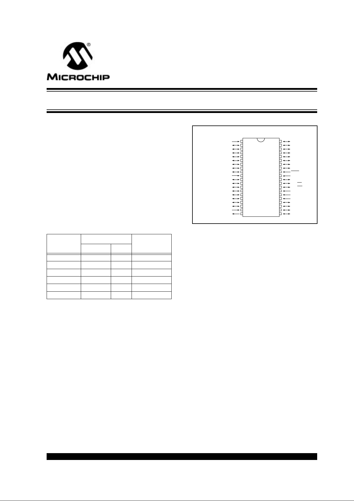
Pin Diagram
• TMR2: 8-bit timer/counter
• TMR3: 16-bit timer/counter
• Universal Synchronous Asynchronous Receiver
Transmitter (USART/SCI)
Special Microcontroller Features:
• Power-on Reset (POR), Power-up Timer (PWRT)
and Oscillator Start-up Timer (OST)
• Watchdog Timer (WDT) with its own on-chip RC
oscillator for reliable operation
• Code-protection
• Power saving SLEEP mode
• Selectable oscillator options
CMOS Tec hnology:
• Low-power, high-speed CMOS EPROM/ROM
technology
• Fully static design
• Wide operating voltage range (2.5V to 6.0V)
• Commercial and Industrial Temperature Range
• Low-power consumption
- < 5 mA @ 5V, 4 MHz
- 100 µ A typical @ 4.5V, 32 kHz
- < 1 µ A typical standby current @ 5V
PIC17C4X
RD0/AD8
RD1/AD9
RD2/AD10
RD3/AD11
RD4/AD12
RD5/AD13
RD6/AD14
RD7/AD15
MCLR
/VPP
VSS
RE0/ALE
RE1/OE
RE2/WR
TEST
RA0/INT
RA1/T0CKI
RA2
RA3
RA4/RX/DT
RA5/TX/CK
VDD
RC0/AD0
RC1/AD1
RC2/AD2
RC3/AD3
RC4/AD4
RC5/AD5
RC6/AD6
RC7/AD7
V
SS
RB0/CAP1
RB1/CAP2
RB2/PWM1
RB3/PWM2
RB4/TCLK12
RB5/TCLK3
RB6
RB7
OSC1/CLKIN
OSC2/CLKOUT
1
2
3
4
5
6
7
8
9
10
11
12
13
14
15
16
17
18
19
20
40
39
38
37
36
35
34
33
32
31
30
29
28
27
26
25
24
23
22
21
PDIP, CERDIP, Windowed CERDIP
PIC17C4X
High-Performance 8-Bit CMOS EPROM/ROM Microcontroller
†NOT recommended for new designs, use 17C42A.
PIC17C4X
DS30412C-page 2
1996 Microchip Technology Inc.
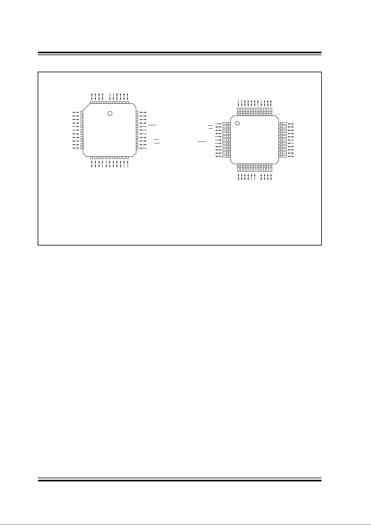
Pin Diagrams Cont.’d
RD4/AD12
RD5/AD13
RD6/AD14
RD7/AD15
MCLR
/VPP
VSS
VSS
RE0/ALE
RE1/OE
RE2/WR
TEST
RC4/AD4
RC5/AD5
RC6/AD6
RC7/AD7
V
SS
VSS
RB0/CAP1
RB1/CAP2
RB2/PWM1
RB3/PWM2
RB4/TCLK12
RC3/AD3
RC2/AD2
RC1/AD1
RC0/AD0
NC
V
DD
VDD
RD0/AD8
RD1/AD9
RD2/AD10
RD3/AD11
7
8
9
10
11
12
13
14
15
16
17
39
38
37
36
35
34
33
32
31
30
29
RA0/INT
RA1/T0CKI
RA2
RA3
RA4/RX/DT
RA5/TX/CK
OSC2/CLKOUT
OSC1/CLKIN
RB7
RB6
RB5/TCLK3
65432
1
4443424140
2827262524232221201918
RB4/TCLK12
RB3/PWM2
RB2/PWM1
RB1/CAP2
RB0/CAP1
V
SS
VSS
RC7/AD7
RC6/AD6
RC5/AD5
RC4/AD4
TEST
RE2/WR
RE1/OE
RE0/ALE
V
SS
VSS
MCLR/VPP
RD7/AD15
RD6/AD14
RD5/AD13
RD4/AD12
RA0/INT
RA1/T0CKI
RA2
RA3
RA4/RX/DT
RA5/TX/CK
OSC2/CLKOUT
OSC1/CLKIN
RB7
RB6
RB5/TCLK3
1
2
3
4
5
6
7
8
9
10
11
33
32
31
30
29
28
27
26
25
24
23
RC3/AD3
RC2/AD2
RC1/AD1
RC0/AD0
NC
VDDVDD
RD0/AD8
RD1/AD9
RD2/AD10
RD3/AD11
4443424140393837363534
2221201918171615141312
PLCC
MQFP
TQFP
All devices are available in all package types, listed in Section 21.0, with the following exceptions:
• ROM devices are not available in Windowed CERDIP Packages
• TQFP is not available for the PIC17C42.
PIC17C4X
PIC17C4X

1996 Microchip Technology Inc. DS30412C-page 3
PIC17C4X
Table of Contents
1.0 Overview..............................................................................................................................................................5
2.0 PIC17C4X Device Varieties.................................................................................................................................7
3.0 Architectural Overview.........................................................................................................................................9
4.0 Reset..................................................................................................................................................................15
5.0 Interrupts............................................................................................................................................................21
6.0 Memory Organization.........................................................................................................................................29
7.0 Table Reads and Table Writes...........................................................................................................................43
8.0 Hardware Multiplier............................................................................................................................................49
9.0 I/O Ports.............................................................................................................................................................53
10.0 Overview of Timer Resources............................................................................................................................65
11.0 Timer0................................................................................................................................................................67
12.0 Timer1, Timer2, Timer3, PWMs and Captures...................................................................................................71
13.0 Universal Synchronous Asynchronous Receiver Transmitter (USART) Module................................................83
14.0 Special Features of the CPU..............................................................................................................................99
15.0 Instruction Set Summary..................................................................................................................................107
16.0 Development Support.......................................................................................................................................143
17.0 PIC17C42 Electrical Characteristics ................................................................................................................147
18.0 PIC17C42 DC and AC Characteristics.............................................................................................................163
19.0 PIC17CR42/42A/43/R43/44 Electrical Characteristics.....................................................................................175
20.0 PIC17CR42/42A/43/R43/44 DC and AC Characteristics.................................................................................193
21.0 Packaging Information......................................................................................................................................205
Appendix A: Modifications..........................................................................................................................................211
Appendix B: Compatibility...........................................................................................................................................211
Appendix C: What’s New............................................................................................................................................212
Appendix D: What’s Changed.....................................................................................................................................212
Appendix E: PIC16/17 Microcontrollers......................................................................................................................213
Appendix F: Errata for PIC17C42 Silicon...................................................................................................................223
Index............................................................................................................................................................................226
PIC17C4X Product Identification System ....................................................................................................................237
For register and module descriptions in this data sheet, device legends show which devices apply to those sections.
For example, the legend below shows that some features of only the PIC17C43, PIC17CR43, PIC17C44 are described
in this section.
Applicable Devices
42
R42 42A 43 R43 44
To Our Valued Customers
We constantly strive to improve the quality of all our products and documentation. We have spent an excep-
tional amount of time to ensure that these documents are correct. However, we realize that we may have
missed a few things. If you find any information that is missing or appears in error from the previous version of
the PIC17C4X Data Sheet (Literature Number DS30412B), please use the reader response form in the back
of this data sheet to inform us. We appreciate your assistance in making this a better document.
To assist you in the use of this document, Appendix C contains a list of new information in this data sheet,
while Appendix D contains information that has changed

PIC17C4X
DS30412C-page 4
1996 Microchip Technology Inc.
NOTES:

1996 Microchip Technology Inc. DS30412C-page 5
PIC17C4X
1.0 OVERVIEW
This data sheet covers the PIC17C4X group of the
PIC17CXX family of microcontrollers. The following
devices are discussed in this data sheet:
• PIC17C42
• PIC17CR42
• PIC17C42A
• PIC17C43
• PIC17CR43
• PIC17C44
The PIC17CR42, PIC17C42A, PIC17C43,
PIC17CR43, and PIC17C44 devices include architectural enhancements over the PIC17C42. These
enhancements will be discussed throughout this data
sheet.
The PIC17C4X devices are 40/44-Pin,
EPROM/ROM-based members of the versatile
PIC17CXX family of low-cost, high-performance,
CMOS, fully-static, 8-bit microcontrollers.
All PIC16/17 microcontrollers employ an advanced
RISC architecture. The PIC17CXX has enhanced core
features, 16-level deep stack, and multiple internal and
external interrupt sources. The separate instruction and
data buses of the Harvard architecture allow a 16-bit
wide instruction word with a separate 8-bit wide data.
The two stage instruction pipeline allows all instructions
to execute in a single cycle, except for program
branches (which require two cycles). A total of 55
instructions (reduced instruction set) are available in
the PIC17C42 and 58 instructions in all the other
devices. Additionally, a large register set gives some of
the architectural innovations used to achieve a very
high performance. For mathematical intensive applications all devices, except the PIC17C42, have a single
cycle 8 x 8 Hardware Multiplier.
PIC17CXX microcontrollers typically achieve a 2:1
code compression and a 4:1 speed improvement over
other 8-bit microcontrollers in their class.
PIC17C4X devices have up to 454 bytes of RAM and
33 I/O pins. In addition, the PIC17C4X adds several
peripheral features useful in many high performance
applications including:
• Four timer/counters
• Two capture inputs
• Two PWM outputs
• A Universal Synchronous Asynchronous Receiver
Transmitter (USART)
These special features reduce external components,
thus reducing cost, enhancing system reliability and
reducing power consumption. There are four oscillator
options, of which the single pin RC oscillator provides a
low-cost solution, the LF oscillator is for low frequency
crystals and minimizes power consumption, XT is a
standard crystal, and the EC is for external clock input.
The SLEEP (power-down) mode offers additional
power saving. The user can wake-up the chip from
SLEEP through several external and internal interrupts
and device resets.
There are four configuration options for the de vice operational modes:
• Microprocessor
• Microcontroller
• Extended microcontroller
• Protected microcontroller
The microprocessor and extended microcontroller
modes allow up to 64K-words of external program
memory.
A highly reliable Watchdog Timer with its own on-chip
RC oscillator provides protection against software malfunction.
Table 1-1 lists the features of the PIC17C4X devices.
A UV-erasable CERDIP-packaged version is ideal for
code development while the cost-effective One-Time
Programmable (OTP) version is suitable for production
in any volume.
The PIC17C4X fits perfectly in applications ranging
from precise motor control and industrial process control to automotive, instrumentation, and telecom applications. Other applications that require extremely fast
execution of complex software programs or the flexibility of programming the software code as one of the last
steps of the manufacturing process would also be well
suited. The EPROM technology makes customization
of application programs (with unique security codes,
combinations, model numbers, parameter storage,
etc.) fast and convenient. Small footprint package
options make the PIC17C4X ideal for applications with
space limitations that require high performance. High
speed execution, powerful peripheral features, flexible
I/O, and low power consumption all at low cost make
the PIC17C4X ideal for a wide range of embedded control applications.
1.1 F
amily and Upward Compatibility
Those users familiar with the PIC16C5X and
PIC16CXX families of microcontrollers will see the
architectural enhancements that have been implemented. These enhancements allow the device to be
more efficient in software and hardware requirements.
Please refer to Appendix A for a detailed list of
enhancements and modifications. Code written for
PIC16C5X or PIC16CXX can be easily ported to
PIC17CXX family of devices (Appendix B).
1.2 De
velopment Support
The PIC17CXX family is supported by a full-featured
macro assembler, a software simulator, an in-circuit
emulator, a universal programmer, a “C” compiler, and
fuzzy logic support tools.
PIC17C4X
DS30412C-page 6
1996 Microchip Technology Inc.
TABLE 1-1: PIC17CXX FAMILY OF DEVICES
Features PIC17C42 PIC17CR42 PIC17C42A PIC17C43 PIC17CR43 PIC17C44
Maximum Frequency of Operation 25 MHz 33 MHz 33 MHz 33 MHz 33 MHz 33 MHz
Operating Voltage Range 4.5 - 5.5V 2.5 - 6.0V 2.5 - 6.0V 2.5 - 6.0V 2.5 - 6.0V 2.5 - 6.0V
Program Memory x16 (EPROM) 2K - 2K 4K - 8K
(ROM)-2K- -4KData Memory (bytes) 232 232 232 454 454 454
Hardware Multiplier (8 x 8) - Yes Yes Yes Yes Yes
Timer0 (16-bit + 8-bit postscaler) Yes Yes Yes Yes Yes Yes
Timer1 (8-bit) Yes Yes Yes Yes Yes Yes
Timer2 (8-bit) Yes Yes Yes Yes Yes Yes
Timer3 (16-bit) Yes Yes Yes Yes Yes Yes
Capture inputs (16-bit) 222222
PWM outputs (up to 10-bit) 222222
USART/SCI Yes Yes Yes Yes Yes Yes
Power-on Reset Yes Yes Yes Yes Yes Yes
Watchdog Timer Yes Y es Y es Y es Y es Y es
External Interrupts Yes Yes Yes Yes Yes Yes
Interrupt Sources 11 11 11 11 11 11
Program Memory Code Protect Yes Yes Yes Yes Yes Yes
I/O Pins 33 33 33 33 33 33
I/O High Current Capabil-
ity
Source 25 mA 25 mA 25 mA 25 mA 25 mA 25 mA
Sink
25 mA
(1)
25 mA
(1)
25 mA
(1)
25 mA
(1)
25 mA
(1)
25 mA
(1)
Package Types 40-pin DIP
44-pin PLCC
44-pin MQFP
40-pin DIP
44-pin PLCC
44-pin MQFP
44-pin TQFP
40-pin DIP
44-pin PLCC
44-pin MQFP
44-pin TQFP
40-pin DIP
44-pin PLCC
44-pin MQFP
44-pin TQFP
40-pin DIP
44-pin PLCC
44-pin MQFP
44-pin TQFP
40-pin DIP
44-pin PLCC
44-pin MQFP
44-pin TQFP
Note 1: Pins RA2 and RA3 can sink up to 60 mA.

1996 Microchip Technology Inc. DS30412C-page 7
PIC17C4X
2.0 PIC17C4X DEVICE VARIETIES
A variety of frequency ranges and packaging options
are available . Depending on application and production
requirements, the proper device option can be selected
using the information in the PIC17C4X Product Selection System section at the end of this data sheet. When
placing orders, please use the “PIC17C4X Product
Identification System” at the back of this data sheet to
specify the correct part number.
For the PIC17C4X family of devices, there are four
device “types” as indicated in the device number:
1. C , as in PIC17 C 42. These devices have
EPROM type memory and operate over the
standard voltage range.
2. LC , as in PIC17 LC 42. These devices have
EPROM type memory, operate over an
extended voltage range , and reduced frequency
range.
3. CR , as in PIC17 CR 42. These devices have
ROM type memory and operate over the standard voltage range.
4. LCR , as in PIC17 LCR 42. These devices have
ROM type memory, operate over an extended
voltage range, and reduced frequency range.
2.1 UV Erasab
le Devices
The UV erasable version, offered in CERDIP package,
is optimal for prototype development and pilot programs.
The UV erasable version can be erased and reprogrammed to any of the configuration modes.
Microchip's PRO MATE programmer supports programming of the PIC17C4X. Third party programmers
also are available; refer to the
Third Party Guide
for a
list of sources.
2.2 One-Time-Pr
ogrammable (OTP)
Devices
The availability of OTP devices is especially useful for
customers expecting frequent code changes and
updates.
The OTP devices, packaged in plastic packages, permit the user to program them once. In addition to the
program memory, the configuration bits must also be
programmed.
2.3 Quic
k-Turnaround-Production (QTP)
Devices
Microchip offers a QTP Programming Service for factory production orders. This service is made available
for users who choose not to program a medium to high
quantity of units and whose code patterns have stabilized. The devices are identical to the OTP devices but
with all EPROM locations and configuration options
already programmed by the factory. Certain code and
prototype verification procedures apply before production shipments are available. Please contact your local
Microchip Technology sales office for more details.
2.4 Serializ
ed Quick-Turnaround
Production (SQTP
SM
) De
vices
Microchip offers a unique programming service where
a few user-defined locations in each device are programmed with different serial numbers. The serial numbers may be random, pseudo-random or sequential.
Serial programming allows each device to have a
unique number which can serve as an entry-code,
password or ID number.
ROM devices do not allow serialization information in
the program memory space.
For information on submitting ROM code, please contact your regional sales office.
2.5 Read Onl
y Memory (ROM) Devices
Microchip offers masked ROM versions of several of
the highest volume parts, thus giving customers a low
cost option for high volume, mature products.
For information on submitting ROM code, please contact your regional sales office.

PIC17C4X
DS30412C-page 8
1996 Microchip Technology Inc.
NOTES:

1996 Microchip Technology Inc. DS30412C-page 9
PIC17C4X
3.0 ARCHITECTURAL OVERVIEW
The high performance of the PIC17C4X can be attributed to a number of architectural features commonly
found in RISC microprocessors. To begin with, the
PIC17C4X uses a modified Harvard architecture. This
architecture has the program and data accessed from
separate memories. So the device has a program
memory bus and a data memory bus. This improves
bandwidth over traditional von Neumann architecture,
where program and data are fetched from the same
memory (accesses over the same bus). Separating
program and data memory further allows instructions to
be sized differently than the 8-bit wide data word.
PIC17C4X opcodes are 16-bits wide, enabling single
word instructions. The full 16-bit wide program memory
bus fetches a 16-bit instruction in a single cycle. A twostage pipeline overlaps fetch and execution of instructions. Consequently, all instructions execute in a single
cycle (121 ns @ 33 MHz), except for progr am branches
and two special instructions that transfer data between
program and data memory.
The PIC17C4X can address up to 64K x 16 of program
memory space.
The PIC17C42 and PIC17C42A integrate 2K x 16 of
EPROM program memory on-chip, while the
PIC17CR42 has 2K x 16 of ROM program memory on-
chip.
The PIC17C43 integrates 4K x 16 of EPROM program
memory, while the PIC17CR43 has 4K x 16 of ROM
program memory.
The PIC17C44 integrates 8K x 16 EPROM program
memory.
Program execution can be internal only (microcontroller or protected microcontroller mode), external only
(microprocessor mode) or both (extended microcontroller mode). Extended microcontroller mode does not
allow code protection.
The PIC17CXX can directly or indirectly address its
register files or data memory. All special function registers, including the Program Counter (PC) and Wor king
Register (WREG), are mapped in the data memory.
The PIC17CXX has an orthogonal (symmetrical)
instruction set that makes it possible to carry out any
operation on any register using any addressing mode.
This symmetrical nature and lack of ‘special optimal situations’ mak e prog ramming with the PIC17CXX simple
yet efficient. In addition, the learning curve is reduced
significantly.
One of the PIC17CXX family architectural enhancements from the PIC16CXX family allows two file registers to be used in some two operand instructions. This
allows data to be moved directly between two registers
without going through the WREG register. This
increases performance and decreases program memory usage.
The PIC17CXX devices contain an 8-bit ALU and working register. The ALU is a general purpose arithmetic
unit. It performs arithmetic and Boolean functions
between data in the working register and any register
file.
The ALU is 8-bits wide and capable of addition, subtraction, shift, and logical operations. Unless otherwise
mentioned, arithmetic operations are two's complement in nature.
The WREG register is an 8-bit working register used for
ALU operations.
All PIC17C4X devices (except the PIC17C42) have an
8 x 8 hardware multiplier. This multiplier generates a
16-bit result in a single cycle.
Depending on the instruction executed, the ALU may
affect the values of the Carry (C), Digit Carry (DC), and
Zero (Z) bits in the STATUS register. The C and DC bits
operate as a borro
w and digit borrow out bit, respectively, in subtraction. See the SUBLW and SUBWF
instructions for examples.
Although the ALU does not perform signed arithmetic,
the Overflow bit (OV) can be used to implement signed
math. Signed arithmetic is comprised of a magnitude
and a sign bit. The overflow bit indicates if the magnitude overflows and causes the sign bit to change state.
Signed math can have greater than 7-bit values (magnitude), if more than one byte is used. The use of the
overflow bit only operates on bit6 (MSb of magnitude)
and bit7 (sign bit) of the value in the ALU. That is, the
overflow bit is not useful if trying to implement signed
math where the magnitude, for example, is 11-bits. If
the signed math values are greater than 7-bits (15-, 24or 31-bit), the algorithm must ensure that the low order
bytes ignore the overflow status bit.
Care should be taken when adding and subtracting
signed numbers to ensure that the correct operation is
executed. Example 3-1 shows an item that must be
taken into account when doing signed arithmetic on an
ALU which operates as an unsigned machine.
EXAMPLE 3-1: SIGNED MATH
Signed math requires the result in REG to
be FEh (-126). This would be accomplished
by subtracting one as opposed to adding
one.
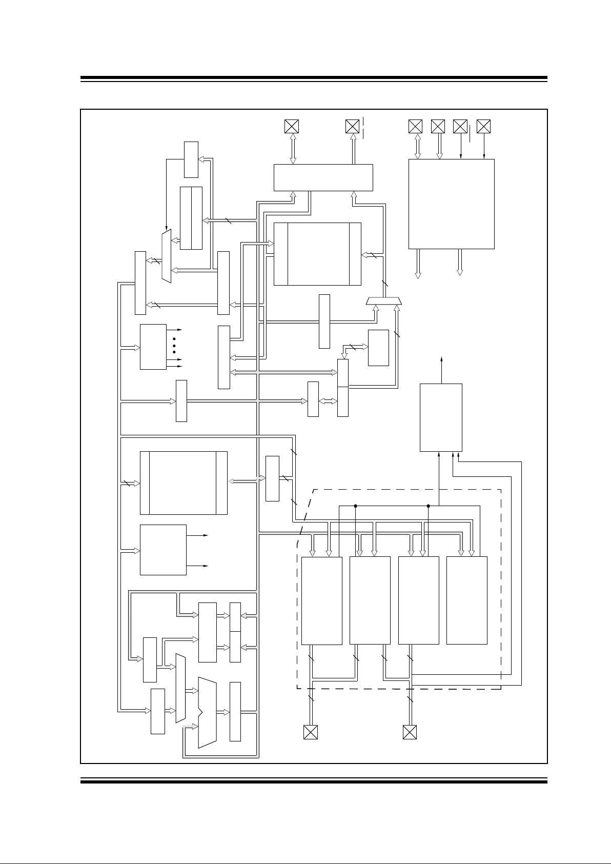
Simplified block diagrams are shown in Figure 3-1 and
Figure 3-2. The descriptions of the device pins are
listed in Table 3-1.
Hex Value Signed Value
Math
Unsigned Value
Math
FFh
+ 01h
= ?
-127
+ 1
= -126 (FEh)
255
+ 1
= 0 (00h);
Carry bit = 1

PIC17C4X
DS30412C-page 10
1996 Microchip Technology Inc.
FIGURE 3-1: PIC17C42 BLOCK DIAGRAM
CLOCK GENERATOR
POWER ON RESET
WATCHDOG TIMER
OSC STARTUP TIMER
TEST MODE SELECT
SYSTEM
DATA LATCH
ADDRESS LATCH
PROGRAM
MEMORY
(EPROM/ROM)
TABLE PTR<16>
STACK
16 x 16
PCH PCL
PCLATH<8>
TABLE LATCH <16>
ROM LATCH <16>
LITERAL
INSTRUCTION
DECODER
CONTROL OUTPUTS
IR LATCH <16>
FSR0
FSR1
8
8
8
IR BUS <16>
RAM ADDR BUFFER
DATA LATCH
READ/WRITE
DECODE
FOR REGISTERS
MAPPED
IN DATA
SPACE
WREG <8>
BITOP
ALU
SHIFTER
IR BUS <16>
PORTB
PORTA
RB0/CAP1
RB1/CAP2
RB2/PWM1
RB2/PWM2
RB4/TCLK12
RB5/TCLK3
RB6
RB7
RA0/INT
RA1/T0CKI
RA2
RA3
RA4/RX/DT
RA5/TX/CK
RA1/
Timer1, Timer2, Timer3
CAPTURE
PWM
DIGITAL I/O
PORTS A, B
SERIAL PORT
Timer0 MODULE
DATA BUS <8>
IR BUS <7:0>
RA1/T0CKI
RA0/INT
86
8
6
2
6
4
3
IR <2:0>
DATA BUS <8>
CONTROL
SIGNALS
TO CPU
CHIP_RESET
AND OTHER
CONTROL
SIGNALS
Q1, Q2, Q3, Q4
16
16
11
AD <15:0>
PORTC and
ALE, WR
, OE
PORTE
OSC1, OSC2
V
DD, VSS
MCLR/VPP
TEST
DECODE
BSR
INTERRUPT
MODULE
8
RDF
WRF
T0CKI
PERIPHERALS
IR <7>
BUS
INTER-
FACE
16
DATA RAM
232x8
2K x 16
PORTD
1996 Microchip Technology Inc. DS30412C-page 11
PIC17C4X
FIGURE 3-2: PIC17CR42/42A/43/R43/44 BLOCK DIAGRAM
CLOCK GENERATOR
POWER ON RESET
WATCHDOG TIMER
OSC STARTUP TIMER
TEST MODE SELECT
SYSTEM
DATA LATCH
ADDRESS LATCH
PROGRAM
MEMORY
(EPROM/ROM)
TABLE PTR<16>
STACK
16 x 16
PCH PCL
PCLATH<8>
TABLE LATCH <16>
ROM LATCH <16>
LITERAL
INSTRUCTION
DECODER
CONTROL OUTPUTS
IR LATCH <16>
FSR0
FSR1
8
8
8
IR BUS <16>
RAM ADDR BUFFER
DATA LATCH
READ/WRITE
DECODE
FOR REGISTERS
MAPPED
IN DATA
SPACE
WREG <8>
BITOP
ALU
SHIFTER
IR BUS <16>
PORTB
PORTA
RB0/CAP1
RB1/CAP2
RB2/PWM1
RB2/PWM2
RB4/TCLK12
RB5/TCLK3
RB6
RB7
RA0/INT
RA1/T0CKI
RA2
RA3
RA4/RX/DT
RA5/TX/CK
RA1/
Timer1, Timer2, Timer3
CAPTURE
PWM
DIGITAL I/O
PORTS A, B
SERIAL PORT
Timer0 MODULE
DATA BUS <8>
BSR<7:4>
RA1/T0CKI
RA0/INT
86
8
6
2
6
4
3
IR <2:0>
DATA BUS <8>
CONTROL
SIGNALS
TO CPU
CHIP_RESET
AND OTHER
CONTROL
SIGNALS
Q1, Q2, Q3, Q4
16
16
13
AD <15:0>
PORTC and
ALE, WR
, OE
PORTE
OSC1, OSC2
V
DD, VSS
MCLR/VPP
TEST
DECODE
BSR
INTERRUPT
MODULE
12
RDF
WRF
T0CKI
PERIPHERALS
IR <7>
BUS
INTER-
FACE
16
8 x 8 mult
PRODH PRODL
DATA RAM
454 x 8 PIC17C43
8K x 16 - PIC17C44
4K x 16 - PIC17C43
IR BUS<7:0>
4K x 16 - PIC17CR43
454 x 8 PIC17CR43
454 x 8 PIC17C44
232 x 8 PIC17C42A
232 x 8 PIC17CR42
2K x 16 - PIC17C42A
2K x 16 - PIC17CR42
PORTD

PIC17C4X
DS30412C-page 12
1996 Microchip Technology Inc.
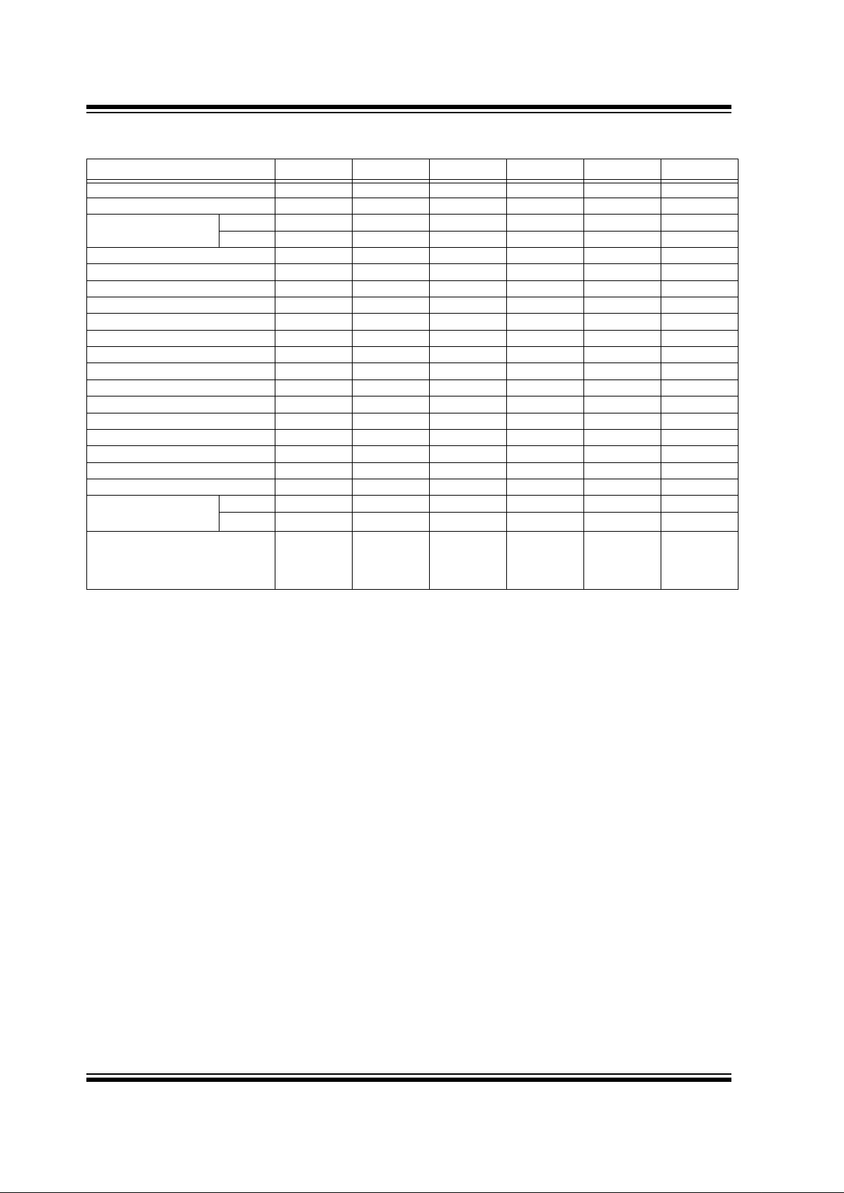
TABLE 3-1:
PINOUT DESCRIPTIONS
Name
DIP
No.
PLCC
No.
QFP
No.
I/O/P
Type
Buffer
Type
Description
OSC1/CLKIN 19 21 37 I ST Oscillator input in crystal/resonator or RC oscillator mode.
External clock input in external clock mode.
OSC2/CLKOUT 20 22 38 O — Oscillator output. Connects to crystal or resonator in crystal
oscillator mode. In RC oscillator or external clock modes
OSC2 pin outputs CLKOUT which has one fourth the frequency of OSC1 and denotes the instruction cycle rate.
MCLR
/V
PP
32 35 7 I/P ST Master clear (reset) input/Programming Voltage (V
PP
) input.
This is the active low reset input to the chip.
PORTA is a bi-directional I/O Port except for RA0 and RA1
which are input only.
RA0/INT 26 28 44 I ST RA0/INT can also be selected as an external interrupt
input. Interrupt can be configured to be on positive or
negative edge.
RA1/T0CKI 25 27 43 I ST RA1/T0CKI can also be selected as an external interrupt
input, and the interrupt can be configured to be on positive or negative edge. RA1/T0CKI can also be selected
to be the clock input to the Timer0 timer/counter.
RA2 24 26 42 I/O ST High voltage, high current, open drain input/output port
pins.
RA3 23 25 41 I/O ST High voltage, high current, open drain input/output port
pins.
RA4/RX/DT 22 24 40 I/O ST RA4/RX/DT can also be selected as the USART (SCI)
Asynchronous Receive or USART (SCI) Synchronous
Data.
RA5/TX/CK 21 23 39 I/O ST RA5/TX/CK can also be selected as the USART (SCI)
Asynchronous Transmit or USART (SCI) Synchronous
Clock.
PORTB is a bi-directional I/O Port with software configurable
weak pull-ups.
RB0/CAP1 11 13 29 I/O ST RB0/CAP1 can also be the CAP1 input pin.
RB1/CAP2 12 14 30 I/O ST RB1/CAP2 can also be the CAP2 input pin.
RB2/PWM1 13 15 31 I/O ST RB2/PWM1 can also be the PWM1 output pin.
RB3/PWM2 14 16 32 I/O ST RB3/PWM2 can also be the PWM2 output pin.
RB4/TCLK12 15 17 33 I/O ST RB4/TCLK12 can also be the external clock input to
Timer1 and Timer2.
RB5/TCLK3 16 18 34 I/O ST RB5/TCLK3 can also be the external clock input to
Timer3.
RB6 17 19 35 I/O ST
RB7 18 20 36 I/O ST
PORTC is a bi-directional I/O Port.
RC0/AD0 2 3 19 I/O TTL This is also the lower half of the 16-bit wide system bus
in microprocessor mode or extended microcontroller
mode. In multiplexed system bus configuration, these
pins are address output as well as data input or output.
RC1/AD1 3 4 20 I/O TTL
RC2/AD2 4 5 21 I/O TTL
RC3/AD3 5 6 22 I/O TTL
RC4/AD4 6 7 23 I/O TTL
RC5/AD5 7 8 24 I/O TTL
RC6/AD6 8 9 25 I/O TTL
RC7/AD7 9 10 26 I/O TTL
Legend: I = Input only; O = Output only; I/O = Input/Output; P = Power; — = Not Used; TTL = TTL input;
ST = Schmitt Trigger input.
1996 Microchip Technology Inc. DS30412C-page 13
PIC17C4X
PORTD is a bi-directional I/O Port.
RD0/AD8 40 43 15 I/O TTL This is also the upper byte of the 16-bit system bus in
microprocessor mode or extended microprocessor mode
or extended microcontroller mode. In multiplexed system
bus configuration these pins are address output as well
as data input or output.
RD1/AD9 39 42 14 I/O TTL
RD2/AD10 38 41 13 I/O TTL
RD3/AD11 37 40 12 I/O TTL
RD4/AD12 36 39 11 I/O TTL
RD5/AD13 35 38 10 I/O TTL
RD6/AD14 34 37 9 I/O TTL
RD7/AD15 33 36 8 I/O TTL
PORTE is a bi-directional I/O Port.
RE0/ALE 30 32 4 I/O TTL In microprocessor mode or extended microcontroller
mode, it is the Address Latch Enable (ALE) output.
Address should be latched on the falling edge of ALE
output.
RE1/OE
29 31 3 I/O TTL In microprocessor or extended microcontroller mode, it is
the Output Enable (OE
) control output (active low).
RE2/WR
28 30 2 I/O TTL In microprocessor or extended microcontroller mode, it is
the Write Enable (WR
) control output (active low).
TEST 27 29 1 I ST Test mode selection control input. Always tie to V
SS
for nor-
mal operation.
V
SS
10, 3111,
12,
33, 34
5, 6,
27, 28
P Ground reference for logic and I/O pins.
V
DD
1 1, 44 16, 17 P Positive supply for logic and I/O pins.
TABLE 3-1:
PINOUT DESCRIPTIONS
Name
DIP
No.
PLCC
No.
QFP
No.
I/O/P
Type
Buffer
Type
Description
Legend: I = Input only; O = Output only; I/O = Input/Output; P = Power; — = Not Used; TTL = TTL input;
ST = Schmitt Trigger input.
PIC17C4X
DS30412C-page 14
1996 Microchip Technology Inc.
3.1 Cloc
king Scheme/Instruction Cycle
The clock input (from OSC1) is internally divided by
four to generate four non-overlapping quadrature
clocks, namely Q1, Q2, Q3, and Q4. Internally, the program counter (PC) is incremented every Q1, and the
instruction is fetched from the program memory and
latched into the instruction register in Q4. The instr uction is decoded and executed during the following Q1
through Q4. The clocks and instruction execution flow
are shown in Figure 3-3.
3.2 Instruction Flo
w/Pipelining
An “Instruction Cycle” consists of four Q cycles (Q1,
Q2, Q3, and Q4). The instruction fetch and execute are
pipelined such that fetch takes one instruction cycle
while decode and execute takes another instruction
cycle. However, due to the pipelining, each instruction
effectively executes in one cycle. If an instruction
causes the program counter to change (e.g. GOTO ) then
two cycles are required to complete the instruction
(Example 3-2).
A fetch cycle begins with the program counter incrementing in Q1.
In the execution cycle, the f etched instruction is latched
into the “Instruction Register (IR)” in cycle Q1. This
instruction is then decoded and executed during the
Q2, Q3, and Q4 cycles. Data memory is read during Q2
(operand read) and written during Q4 (destination
write).
FIGURE 3-3: CLOCK/INSTRUCTION CYCLE
EXAMPLE 3-2: INSTRUCTION PIPELINE FLOW
Q1
Q2 Q3 Q4
Q1
Q2 Q3 Q4
Q1
Q2 Q3 Q4
OSC1
Q1
Q2
Q3
Q4
PC
OSC2/CLKOUT
(RC mode)
PC PC+1 PC+2
Fetch INST (PC)
Execute INST (PC-1) Fetch INST (PC+1)
Execute INST (PC) Fetch INST (PC+2)
Execute INST (PC+1)
Internal
phase
clock
All instructions are single cycle, except for any program branches. These take two cycles since the fetch
instruction is “flushed” from the pipeline while the new instruction is being fetched and then executed.
Tcy0 Tcy1 Tcy2 Tcy3 Tcy4 Tcy5
1. MOVLW 55h
Fetch 1 Execute 1
2. MOVWF PORTB
Fetch 2 Execute 2
3. CALL SUB_1
Fetch 3 Execute 3
4. BSF PORTA, BIT3 (Forced NOP)
Fetch 4 Flush
5. Instruction @ address SUB_1
Fetch SUB_1 Execute SUB_1
1996 Microchip Technology Inc. DS30412C-page 15
PIC17C4X
4.0 RESET
The PIC17CXX differentiates between various kinds of
reset:
• Power-on Reset (POR)
• MCLR
reset during normal operation
• WDT Reset (normal operation)
Some registers are not affected in any reset condition;
their status is unknown on POR and unchanged in any
other reset. Most other registers are forced to a “reset
state” on Power-on Reset (POR), on MCLR
or WDT
Reset and on M
CLR reset during SLEEP. They are not
affected by a WDT Reset during SLEEP, since this reset
is viewed as the resumption of normal operation. The
T
O and PD bits are set or cleared differently in diff erent
reset situations as indicated in T ab le 4-3. These bits are
used in software to determine the nature of reset. See
Table 4-4 for a full description of reset states of all registers.
A simplified block diagram of the on-chip reset circuit is
shown in Figure 4-1.
Note: While the device is in a reset state, the
internal phase clock is held in the Q1 state.
Any processor mode that allows external
execution will force the RE0/ALE pin as a
low output and the RE1/OE
and RE2/WR
pins as high outputs.
4.1 P
ower-on Reset (POR), Power-up
Timer (PWRT), and Oscillator Start-up
Timer (OST)
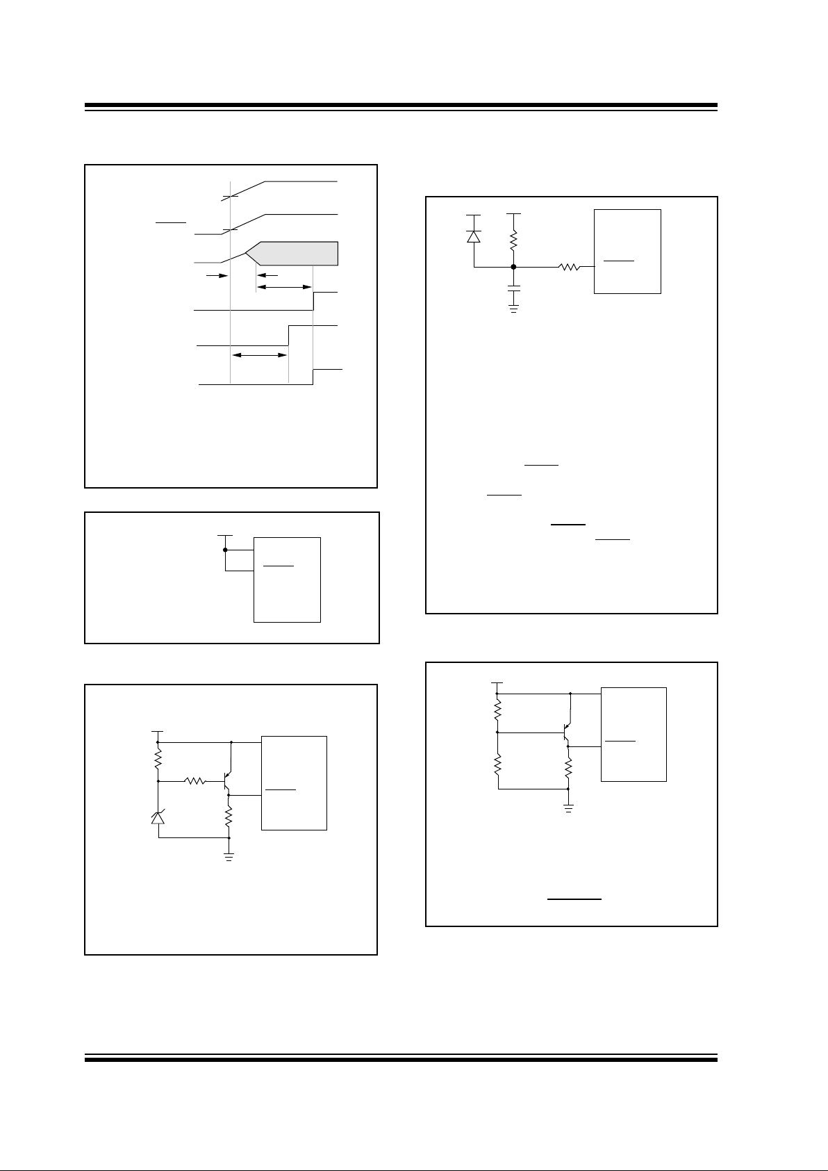
4.1.1 POWER-ON RESET (POR)
The Power-on Reset circuit holds the device in reset
until V
DD
is above the trip point (in the range of 1.4V -
2.3V). The PIC17C42 does not produce an internal
reset when V
DD
declines. All other devices will produce
an internal reset for both rising and falling V
DD
. To take
advantage of the POR, just tie the MCLR
/V
PP
pin
directly (or through a resistor) to V
DD
. This will eliminate
external RC components usually needed to create
Power-on Reset. A minimum rise time for V
DD
is
required. See Electrical Specifications for details.
4.1.2 PO WER-UP TIMER (PWRT)
The Power-up Timer provides a fixed 96 ms time-out
(nominal) on power-up. This occurs from rising edge of
the POR signal and after the first rising edge of MCLR
(detected high). The Power-up Timer operates on an
internal RC oscillator. The chip is kept in RESET as
long as the PWRT is active. In most cases the PWRT
delay allows the V
DD
to rise to an acceptable level.
The power-up time delay will v ary from chip to chip and
to V
DD
and temperature. See DC parameters for
details.
FIGURE 4-1: SIMPLIFIED BLOCK DIAGRAM OF ON-CHIP RESET CIRCUIT
S
R
Q
External
Reset
MCLR
VDD
OSC1
WDT
Module
V
DD rise
detect
OST/PWRT
On-chip
RC OSC†
WDT
Time_Out
Power_On_Reset
OST
10-bit Ripple counter
PWRT
Chip_Reset
10-bit Ripple counter
Power_Up
(Enable the PWRT timer
only during Power_Up)
(Power_Up + Wake_Up) (XT + LF)
(Enable the OST if it is Power_Up or Wake_Up
from SLEEP and OSC type is XT or LF)
Reset
Enable OST
Enable PWRT
† This RC oscillator is shared with the WDT
when not in a power-up sequence.
PIC17C4X
DS30412C-page 16
1996 Microchip Technology Inc.
4.1.3 OSCILLATOR START-UP TIMER (OST)
The Oscillator Start-up Timer (OST) provides a 1024
oscillator cycle (1024T
OSC
) delay after MCLR
is
detected high or a wake-up from SLEEP event occurs.
The OST time-out is invoked only f or XT and LF oscilla-
tor modes on a Power-on Reset or a Wake-up from
SLEEP.
The OST counts the oscillator pulses on the
OSC1/CLKIN pin. The counter only starts incrementing
after the amplitude of the signal reaches the oscillator
input thresholds. This delay allows the crystal oscillator
or resonator to stabilize before the device exits reset.
The length of time-out is a function of the crystal/resonator frequency.
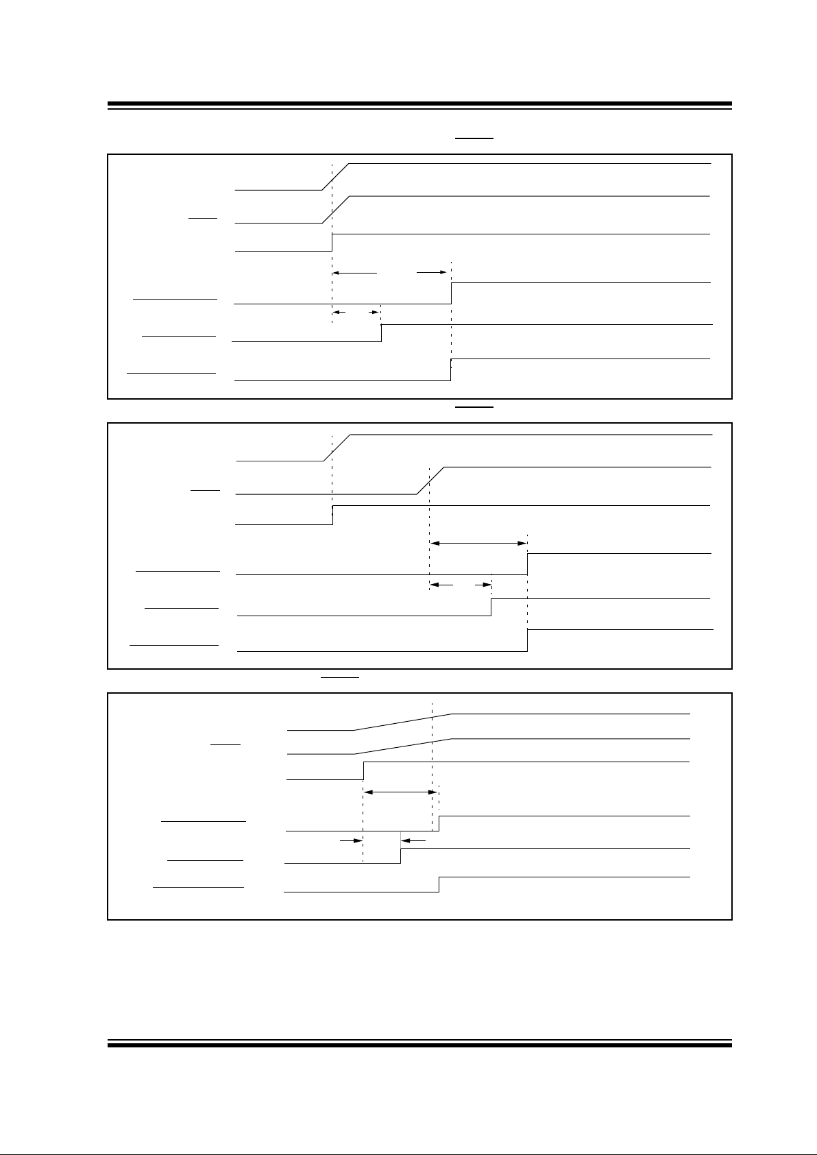
4.1.4 TIME-OUT SEQUENCE
On power-up the time-out sequence is as follows: First
the internal POR signal goes high when the POR trip
point is reached. If MCLR
is high, then both the OST
and PWRT timers start. In general the PWRT time-out
is longer, except with low frequency crystals/resonators. The total time-out also varies based on oscillator
configuration. Table 4-1 shows the times that are associated with the oscillator configuration. Figure 4-2 and
Figure 4-3 display these time-out sequences.
If the device voltage is not within electrical specification
at the end of a time-out, the MCLR
/V
PP
pin must be
held low until the voltage is within the device specification. The use of an external RC delay is sufficient for
many of these applications.
TABLE 4-1: TIME-OUT IN VARIOUS
SITUATIONS
The time-out sequence begins from the first rising edge
of MCLR
.
Table 4-3 shows the reset conditions for some special
registers, while Table 4-4 shows the initialization conditions for all the registers. The shaded registers (in
Table 4-4) are for all devices except the PIC17C42. In
the PIC17C42, the PRODH and PRODL registers are
general purpose RAM.
TABLE 4-2: STATUS BITS AND THEIR
SIGNIFICANCE
In Figure 4-2, Figure 4-3 and Figure 4-4, T
PWRT
>
T
OST
, as would be the case in higher frequency crys-
tals. For lower frequency crystals, (i.e., 32 kHz) T
OST
would be greater.
Oscillator
Configuration
Power-up Wake up
from
SLEEP
MCLR
Reset
XT, LF Greater of:
96 ms or
1024T
OSC
1024T
OSC
—
EC, RC Greater of:
96 ms or
1024T
OSC
——
TOPD
Event
11
Power-on Reset, MCLR Reset during normal
operation, or
CLRWDT instruction executed
10
MCLR Reset during SLEEP or interrupt wake-up
from SLEEP
01
WDT Reset during normal operation
00
WDT Reset during SLEEP
T AB LE 4-3: RESET CONDITION FOR THE PROGRAM COUNTER AND THE CPUSTA REGISTER
Event
PCH:PCL CPUSTA OST Active
Power-on Reset 0000h
--11 11--
Yes
MCLR Reset during normal operation 0000h
--11 11--
No
MCLR
Reset during SLEEP 0000h
--11 10--
Yes
(2)
WDT Reset during normal operation 0000h
--11 01--
No
WDT Reset during SLEEP
(3)
0000h
--11 00--
Yes
(2)
Interrupt wake-up from SLEEP GLINTD is set PC + 1
--11 10--
Yes
(2)
GLINTD is clear
PC + 1
(1)
--10 10--
Yes
(2)
Legend: u = unchanged, x = unknown, - = unimplemented read as '0'.
Note 1: On wake-up, this instruction is executed. The instruction at the appropriate interrupt vector is fetched and
then executed.
2: The OST is only active when the Oscillator is configured for XT or LF modes.
3: The Program Counter = 0, that is the device branches to the reset vector. This is different from the
mid-range devices.
1996 Microchip Technology Inc. DS30412C-page 17
PIC17C4X
FIGURE 4-2: TIME-OUT SEQUENCE ON POWER-UP (MCLR
TIED TO V
DD
)
FIGURE 4-3: TIME-OUT SEQUENCE ON POWER-UP (MCLR
NOT TIED TO V
DD
)
FIGURE 4-4: SLOW RISE TIME (MCLR
TIED TO V
DD
)
TPWRT
TOST
VDD
MCLR
INTERNAL POR
PWRT TIME-OUT
OST TIME-OUT
INTERNAL RESET
TPWRT
TOST
VDD
MCLR
INTERNAL POR
PWRT TIME-OUT
OST TIME-OUT
INTERNAL RESET
VDD
MCLR
INTERNAL POR
PWR
T TIME-OUT
OST TIME-OUT
INTERNAL RESET
0V
1V
5V
TPWRT
TOST
PIC17C4X
DS30412C-page 18
1996 Microchip Technology Inc.
FIGURE 4-5: OSCILLATOR START-UP TIME
FIGURE 4-6: USING ON-CHIP POR
FIGURE 4-7: BROWN-OUT PROTECTION
CIRCUIT 1
VDD
MCLR
OSC2
OST TIME_OUT
PWRT TIME_OUT
INTERNAL RESET
T
OSC1
T
OST
TPWRT
This figure shows in greater detail the timings involved
with the oscillator start-up timer. In this example the
low frequency crystal start-up time is larger than
power-up time (TPWRT).
Tosc1 = time for the crystal oscillator to react to an
oscillation level detectable by the Oscillator Start-up
Timer (ost).
TOST = 1024TOSC.
VDD
MCLR
PIC17CXX
VDD
This circuit will activate reset when VDD goes below
(Vz + 0.7V) where Vz = Zener voltage.
VDD
33k
10k
40 kΩ
V
DD
MCLR
PIC17CXX
FIGURE 4-8: PIC17C42 EXTERNAL
POWER-ON RESET CIRCUIT
(FOR SLOW V
DD
POWER-UP)
FIGURE 4-9: BROWN-OUT PROTECTION
CIRCUIT 2
Note 1: An external Power-on Reset circuit is
required only if V
DD power-up time is too
slow. The diode D helps discharge the
capacitor quickly when V
DD powers
down.
2: R < 40 kΩ is recommended to ensure
that the voltage drop across R does not
exceed 0.2V (max. leakage current spec.
on the MCLR
/VPP pin is 5 µA). A larger
voltage drop will degrade V
IH level on the
MCLR
/VPP pin.
3: R1 = 100Ω to 1 kΩ will limit any current
flowing into MCLR
from external capaci-
tor C in the event of MCLR
/VPP pin
breakdown due to Electrostatic Discharge (ESD) or (Electrical Overstress)
EOS.
C
R1
R
D
V
DD
MCLR
PIC17C42
VDD
This brown-out circuit is less expensive, albeit less
accurate. Transistor Q1 turns off when VDD is below a
certain level such that:
VDD •
R1
R1 + R2
= 0.7V
R2
40 kΩ
VDD
MCLR
PIC17CXX
R1
Q1
V
DD
1996 Microchip Technology Inc. DS30412C-page 19
PIC17C4X
TABLE 4-4: INITIALIZATION CONDITIONS FOR SPECIAL FUNCTION REGISTERS
Register Address Power-on Reset
MCLR
Reset
WDT Reset
Wake-up from SLEEP
through interrupt
Unbanked
INDF0 00h
0000 0000 0000 0000 0000 0000
FSR0 01h
xxxx xxxx uuuu uuuu uuuu uuuu
PCL 02h
0000h 0000h
PC + 1
(2)
PCLATH 03h
0000 0000 0000 0000 uuuu uuuu
ALUSTA 04h
1111 xxxx 1111 uuuu 1111 uuuu
T0STA 05h
0000 000- 0000 000- 0000 000-
CPUSTA
(3)
06h --11 11-- --11 qq-- --uu qq--
INTSTA 07h 0000 0000 0000 0000
uuuu uuuu
(1)
INDF1 08h 0000 0000 0000 0000 uuuu uuuu
FSR1 09h xxxx xxxx uuuu uuuu uuuu uuuu
WREG 0Ah xxxx xxxx uuuu uuuu uuuu uuuu
TMR0L 0Bh xxxx xxxx uuuu uuuu uuuu uuuu
TMR0H 0Ch xxxx xxxx uuuu uuuu uuuu uuuu
TBLPTRL
(4)
0Dh xxxx xxxx uuuu uuuu uuuu uuuu
TBLPTRH
(4)
0Eh xxxx xxxx uuuu uuuu uuuu uuuu
TBLPTRL
(5)
0Dh 0000 0000 0000 0000 uuuu uuuu
TBLPTRH
(5)
0Eh 0000 0000 0000 0000 uuuu uuuu
BSR 0Fh 0000 0000 0000 0000 uuuu uuuu
Bank 0
PORTA 10h 0-xx xxxx 0-uu uuuu uuuu uuuu
DDRB 11h 1111 1111 1111 1111 uuuu uuuu
PORTB 12h xxxx xxxx uuuu uuuu uuuu uuuu
RCSTA 13h 0000 -00x 0000 -00u uuuu -uuu
RCREG 14h xxxx xxxx uuuu uuuu uuuu uuuu
TXSTA 15h 0000 --1x 0000 --1u uuuu --uu
TXREG 16h xxxx xxxx uuuu uuuu uuuu uuuu
SPBRG 17h xxxx xxxx uuuu uuuu uuuu uuuu
Bank 1
DDRC 10h 1111 1111 1111 1111 uuuu uuuu
PORTC 11h xxxx xxxx uuuu uuuu uuuu uuuu
DDRD 12h 1111 1111 1111 1111 uuuu uuuu
PORTD 13h xxxx xxxx uuuu uuuu uuuu uuuu
DDRE 14h ---- -111 ---- -111 ---- -uuu
PORTE 15h ---- -xxx ---- -uuu ---- -uuu
PIR 16h 0000 0010 0000 0010
uuuu uuuu
(1)
PIE 17h 0000 0000 0000 0000 uuuu uuuu
Legend: u = unchanged, x = unknown, - = unimplemented read as '0', q = value depends on condition.
Note 1: One or more bits in INTSTA, PIR will be affected (to cause wake-up).
2: When the wake-up is due to an interrupt and the GLINTD bit is cleared, the PC is loaded with the interrupt
vector.
3: See Table 4-3 for reset value of specific condition.
4: Only applies to the PIC17C42.
5: Does not apply to the PIC17C42.
PIC17C4X
DS30412C-page 20 1996 Microchip Technology Inc.
Bank 2
TMR1 10h xxxx xxxx uuuu uuuu uuuu uuuu
TMR2 11h xxxx xxxx uuuu uuuu uuuu uuuu
TMR3L 12h xxxx xxxx uuuu uuuu uuuu uuuu
TMR3H 13h xxxx xxxx uuuu uuuu uuuu uuuu
PR1 14h xxxx xxxx uuuu uuuu uuuu uuuu
PR2 15h xxxx xxxx uuuu uuuu uuuu uuuu
PR3/CA1L 16h xxxx xxxx uuuu uuuu uuuu uuuu
PR3/CA1H 17h xxxx xxxx uuuu uuuu uuuu uuuu
Bank 3
PW1DCL 10h xx-- ---- uu-- ---- uu-- ----
PW2DCL 11h xx-- ---- uu-- ---- uu-- ----
PW1DCH 12h xxxx xxxx uuuu uuuu uuuu uuuu
PW2DCH 13h xxxx xxxx uuuu uuuu uuuu uuuu
CA2L 14h xxxx xxxx uuuu uuuu uuuu uuuu
CA2H 15h xxxx xxxx uuuu uuuu uuuu uuuu
TCON1 16h 0000 0000 0000 0000 uuuu uuuu
TCON2 17h 0000 0000 0000 0000 uuuu uuuu
Unbanked
PRODL
(5)
18h xxxx xxxx uuuu uuuu uuuu uuuu
PRODH
(5)
19h xxxx xxxx uuuu uuuu uuuu uuuu
TABLE 4-4: INITIALIZATION CONDITIONS FOR SPECIAL FUNCTION REGISTERS (Cont.’d)
Register Address Power-on Reset
MCLR
Reset
WDT Reset
Wake-up from SLEEP
through interrupt
Legend: u = unchanged, x = unknown, - = unimplemented read as '0', q = value depends on condition.
Note 1: One or more bits in INTSTA, PIR will be affected (to cause wake-up).
2: When the wake-up is due to an interrupt and the GLINTD bit is cleared, the PC is loaded with the interrupt
vector.
3: See Table 4-3 for reset value of specific condition.
4: Only applies to the PIC17C42.
5: Does not apply to the PIC17C42.
1996 Microchip Technology Inc. DS30412C-page 21
PIC17C4X
5.0 INTERRUPTS
The PIC17C4X devices have 11 sources of interrupt:
• External interrupt from the RA0/INT pin
• Change on RB7:RB0 pins
• TMR0 Overflow
• TMR1 Overflow
• TMR2 Overflow
• TMR3 Overflow
• USART Transmit buffer empty
• USART Receive buffer full
• Capture1
• Capture2
• T0CKI edge occurred
There are four registers used in the control and status
of interrupts. These are:
• CPUSTA
• INTSTA
• PIE
• PIR
The CPUSTA register contains the GLINTD bit. This is
the Global Interrupt Disable bit. When this bit is set, all
interrupts are disabled. This bit is par t of the controller
core functionality and is described in the Memory Organization section.
When an interrupt is responded to, the GLINTD bit is
automatically set to disable any further interrupt, the
return address is pushed onto the stack and the PC is
loaded with the interrupt vector address. There are four
interrupt vectors. Each vector address is for a specific
interrupt source (except the peripheral interrupts which
have the same vector address). These sources are:
• External interrupt from the RA0/INT pin
• TMR0 Overflow
• T0CKI edge occurred
• Any peripheral interrupt
When program execution vectors to one of these inter-
rupt vector addresses (except for the peripheral interrupt address), the interrupt flag bit is automatically
cleared. Vectoring to the peripheral interrupt vector
address does not automatically clear the source of the
interrupt. In the peripheral interrupt service routine, the
source(s) of the interrupt can be determined by testing
the interrupt flag bits. The interrupt flag bit(s) must be
cleared in software before re-enabling interrupts to
avoid infinite interrupt requests.
All of the individual interrupt flag bits will be set regardless of the status of their corresponding mask bit or the
GLINTD bit.
For external interrupt events, there will be an interrupt
latency. For two cycle instructions, the latency could be
one instruction cycle longer.
The “return from interrupt” instruction, RETFIE , can be
used to mark the end of the interrupt service routine.
When this instruction is executed, the stack is
“POPed”, and the GLINTD bit is cleared (to re-enable
interrupts).
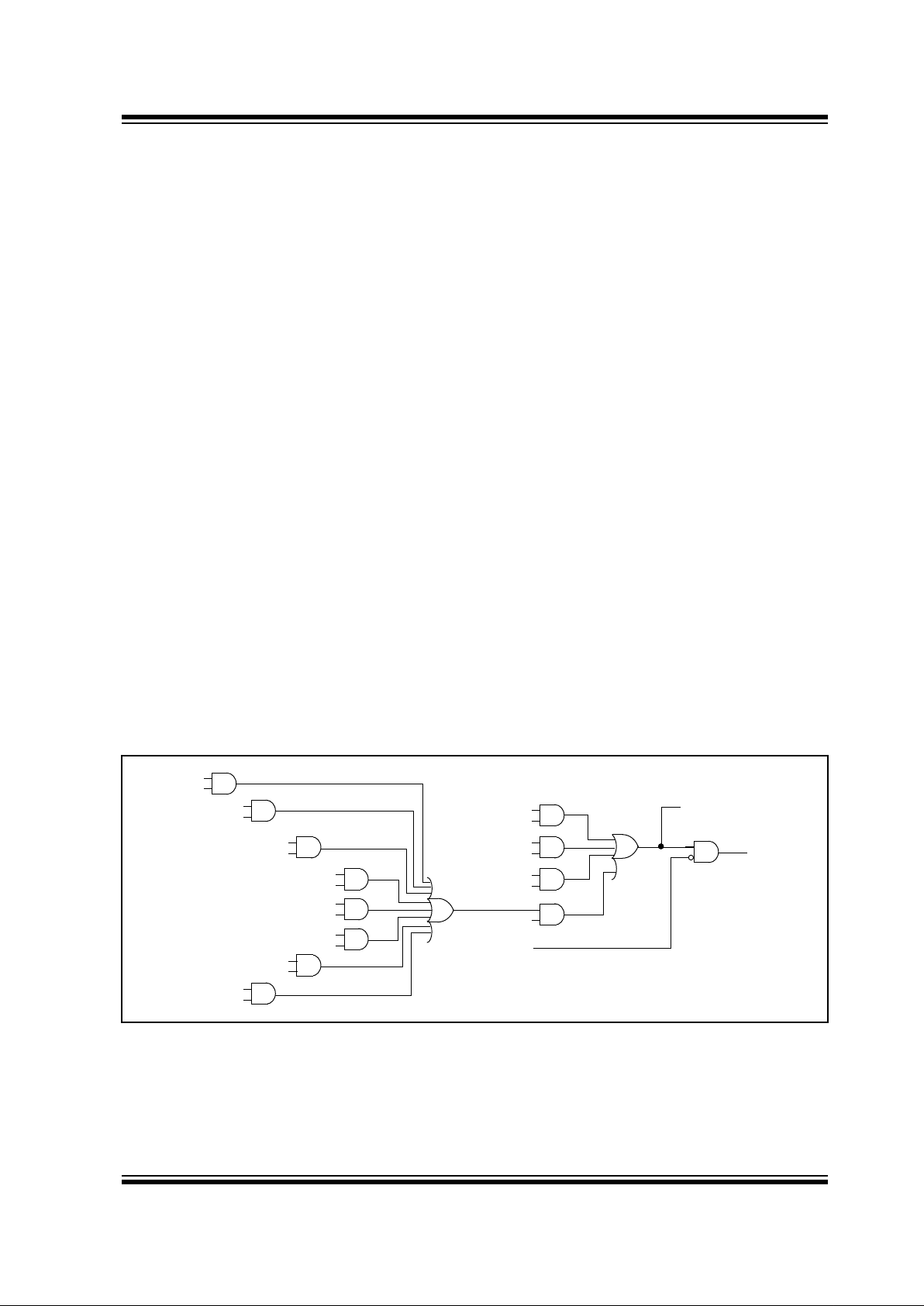
FIGURE 5-1: INTERRUPT LOGIC
TMR1IF
TMR1IE
TMR2IF
TMR2IE
TMR3IF
TMR3IE
CA1IF
CA1IE
CA2IF
CA2IE
TXIF
TXIE
RCIF
RCIE
RBIF
RBIE
T0IF
T0IE
INTF
INTE
T0CKIF
T0CKIE
GLINTD
PEIE
Wake-up (If in SLEEP mode)
or terminate long write
Interrupt to CPU
PEIF

PIC17C4X
DS30412C-page 22
1996 Microchip Technology Inc.
5.1 Interrupt
Status Register (INTSTA)
The Interrupt Status/Control register (INTSTA) records
the individual interrupt requests in flag bits, and contains the individual interrupt enable bits (not for the
peripherals).
The PEIF bit is a read only , bit wise OR of all the peripheral flag bits in the PIR register (Figure 5-4).
Care should be taken when clearing any of the INTSTA
register enable bits when interrupts are enabled
(GLINTD is clear). If any of the INTSTA flag bits (T0IF,
INTF, T0CKIF, or PEIF) are set in the same instruction
cycle as the corresponding interrupt enable bit is
cleared, the device will vector to the reset address
(0x00).
When disabling any of the INTSTA enable bits, the
GLINTD bit should be set (disabled).
Note: T0IF, INTF, T0CKIF, or PEIF will be set by
the specified condition, even if the corresponding interrupt enable bit is clear (interrupt disabled) or the GLINTD bit is set (all
interrupts disabled).
FIGURE 5-2: INTSTA REGISTER (ADDRESS: 07h, UNBANKED)
R - 0 R/W - 0 R/W - 0 R/W - 0 R/W - 0 R/W - 0 R/W - 0 R/W - 0
PEIF T0CKIF T0IF INTF PEIE T0CKIE T0IE INTE
R = Readable bit
W = Writable bit
- n = Value at POR reset
bit7 bit0
bit 7: PEIF : Peripheral Interrupt Flag bit
This bit is the OR of all peripheral interrupt flag bits AND’ed with their corresponding enable bits.
1 =A peripheral interrupt is pending
0 =No peripheral interrupt is pending
bit 6: T0CKIF : External Interrupt on T0CKI Pin Flag bit
This bit is cleared by hardware, when the interrupt logic forces program execution to vector (18h).
1 =The software specified edge occurred on the RA1/T0CKI pin
0 =The software specified edge did not occur on the RA1/T0CKI pin
bit 5: T0IF : TMR0 Overflow Interrupt Flag bit
This bit is cleared by hardware, when the interrupt logic forces program execution to vector (10h).
1 =TMR0 overflowed
0 =TMR0 did not overflow
bit 4: INTF : External Interrupt on INT Pin Flag bit
This bit is cleared by hardware, when the interrupt logic forces program execution to vector (08h).
1 =The software specified edge occurred on the RA0/INT pin
0 =The software specified edge did not occur on the RA0/INT pin
bit 3: PEIE : Peripheral Interrupt Enable bit
This bit enables all peripheral interrupts that have their corresponding enable bits set.
1 =Enable peripheral interrupts
0 =Disable peripheral interrupts
bit 2: T0CKIE : External Interrupt on T0CKI Pin Enable bit
1 =Enable software specified edge interrupt on the RA1/T0CKI pin
0 =Disable interrupt on the RA1/T0CKI pin
bit 1: T0IE : TMR0 Overflow Interrupt Enable bit
1 =Enable TMR0 overflow interrupt
0 =Disable TMR0 overflow interrupt
bit 0: INTE : External Interrupt on RA0/INT Pin Enable bit
1 =Enable software specified edge interrupt on the RA0/INT pin
0 =Disable software specified edge interrupt on the RA0/INT pin

1996 Microchip Technology Inc. DS30412C-page 23
PIC17C4X
5.2 P
eripheral Interrupt Enable Register
(PIE)
This register contains the individual flag bits for the
Peripheral interrupts.
FIGURE 5-3: PIE REGISTER (ADDRESS: 17h, BANK 1)
R/W - 0 R/W - 0 R/W - 0 R/W - 0 R/W - 0 R/W - 0 R/W - 0 R/W - 0
RBIE TMR3IE TMR2IE TMR1IE CA2IE CA1IE TXIE RCIE
R = Readable bit
W = Writable bit
-n = Value at POR reset
bit7 bit0
bit 7: RBIE : PORTB Interrupt on Change Enable bit
1 =Enable PORTB interrupt on change
0 =Disable PORTB interrupt on change
bit 6: TMR3IE : Timer3 Interrupt Enable bit
1 =Enable Timer3 interrupt
0 =Disable Timer3 interrupt
bit 5: TMR2IE : Timer2 Interrupt Enable bit
1 =Enable Timer2 interrupt
0 =Disable Timer2 interrupt
bit 4: TMR1IE : Timer1 Interrupt Enable bit
1 =Enable Timer1 interrupt
0 =Disable Timer1 interrupt
bit 3: CA2IE : Capture2 Interrupt Enable bit
1 =Enable Capture interrupt on RB1/CAP2 pin
0 =Disable Capture interrupt on RB1/CAP2 pin
bit 2: CA1IE : Capture1 Interrupt Enable bit
1 =Enable Capture interrupt on RB2/CAP1 pin
0 =Disable Capture interrupt on RB2/CAP1 pin
bit 1: TXIE : USART Transmit Interrupt Enable bit
1 =Enable Transmit buffer empty interrupt
0 =Disable Transmit buffer empty interrupt
bit 0: RCIE : USART Receive Interrupt Enable bit
1 =Enable Receive buffer full interrupt
0 =Disable Receive buffer full interrupt
PIC17C4X
DS30412C-page 24
1996 Microchip Technology Inc.
5.3 P
eripheral Interrupt Request Register
(PIR)
This register contains the individual flag bits for the
peripheral interrupts.
Note: These bits will be set by the specified con-
dition, even if the corresponding interrupt
enable bit is cleared (interrupt disabled), or
the GLINTD bit is set (all interrupts disabled). Before enabling an interrupt, the
user may wish to clear the interrupt flag to
ensure that the program does not immediately branch to the peripheral interrupt service routine.
FIGURE 5-4: PIR REGISTER (ADDRESS: 16h, BANK 1)
R/W - 0 R/W - 0 R/W - 0 R/W - 0 R/W - 0 R/W - 0 R - 1 R - 0
RBIF TMR3IF TMR2IF TMR1IF CA2IF CA1IF TXIF RCIF
R = Readable bit
W = Writable bit
-n = Value at POR reset
bit7 bit0
bit 7: RBIF : PORTB Interrupt on Change Flag bit
1 =One of the PORTB inputs changed (Software must end the mismatch condition)
0 =None of the PORTB inputs have changed
bit 6: TMR3IF : Timer3 Interrupt Flag bit
If Capture1 is enabled (CA1/PR
3 = 1)
1 =Timer3 overflowed
0 =Timer3 did not overflow
If Capture1 is disabled (CA1/PR
3 = 0)
1 =Timer3 value has rolled over to 0000h from equalling the period register (PR3H:PR3L) value
0 =Timer3 value has not rolled over to 0000h from equalling the period register (PR3H:PR3L) value
bit 5: TMR2IF : Timer2 Interrupt Flag bit
1 =Timer2 value has rolled over to 0000h from equalling the period register (PR2) value
0 =Timer2 value has not rolled over to 0000h from equalling the period register (PR2) value
bit 4: TMR1IF : Timer1 Interrupt Flag bit
If Timer1 is in 8-bit mode (T16 = 0)
1 =Timer1 value has rolled over to 0000h from equalling the period register (PR) value
0 =Timer1 value has not rolled over to 0000h from equalling the period register (PR2) value
If Timer1 is in 16-bit mode (T16 = 1)
1 =TMR1:TMR2 value has rolled over to 0000h from equalling the period register (PR1:PR2) value
0 =TMR1:TMR2 value has not rolled over to 0000h from equalling the period register (PR1:PR2) value
bit 3: CA2IF : Capture2 Interrupt Flag bit
1 =Capture event occurred on RB1/CAP2 pin
0 =Capture event did not occur on RB1/CAP2 pin
bit 2: CA1IF : Capture1 Interrupt Flag bit
1 =Capture event occurred on RB0/CAP1 pin
0 =Capture event did not occur on RB0/CAP1 pin
bit 1: TXIF : USART Transmit Interrupt Flag bit
1 =Transmit buffer is empty
0 =Transmit buffer is full
bit 0: RCIF : USART Receive Interrupt Flag bit
1 =Receive buffer is full
0 =Receive buffer is empty

1996 Microchip Technology Inc. DS30412C-page 25
PIC17C4X
5.4 Interrupt
Operation
Global Interrupt Disable bit, GLINTD (CPUSTA<4>),
enables all unmasked interrupts (if clear) or disables all
interrupts (if set). Individual interrupts can be disabled
through their corresponding enable bits in the INTSTA
register. Peripheral interrupts need either the global
peripheral enable PEIE bit disabled, or the specific
peripheral enable bit disabled. Disabling the peripherals via the global peripheral enable bit, disables all
peripheral interrupts. GLINTD is set on reset (interrupts
disabled).
The RETFIE instruction allows returning from interrupt
and re-enable interrupts at the same time.
When an interrupt is responded to, the GLINTD bit is
automatically set to disable any further interrupt, the
return address is pushed onto the stack and the PC is
loaded with interrupt vector. There are four interrupt
vectors to reduce interrupt latency.
The peripheral interrupt vector has multiple interrupt
sources. Once in the peripheral interrupt service routine, the source(s) of the interrupt can be determined by
polling the interrupt flag bits. The peripheral interr upt
flag bit(s) must be cleared in software before reenabling interrupts to avoid continuous interrupts.
The PIC17C4X devices have four interrupt vectors.
These vectors and their hardware priority are shown in
Table 5-1. If two enabled interrupts occur “at the same
time”, the interrupt of the highest priority will be serviced first. This means that the vector address of that
interrupt will be loaded into the program counter (PC).
TABLE 5-1: INTERRUPT VECTORS/
PRIORITIES
Address Vector Priority
0008h External Interrupt on RA0/
INT pin (INTF)
1 (Highest)
0010h TMR0 overflow interrupt
(T0IF)
2
0018h External Interrupt on T0CKI
(T0CKIF)
3
0020h Peripherals (PEIF) 4 (Lowest)
Note 1: Individual interrupt flag bits are set regard-
less of the status of their corresponding
mask bit or the GLINTD bit.
Note 2: When disabling any of the INTSTA enable
bits, the GLINTD bit should be set
(disabled).
Note 3: For the PIC17C42 only:
If an interrupt occurs while the Global Interrupt Disable (GLINTD) bit is being set, the
GLINTD bit may unintentionally be reenabled by the user’s Interrupt Service
Routine (the RETFIE instruction). The
events that would cause this to occur are:
1. An interrupt occurs simultaneously
with an instruction that sets the
GLINTD bit.
2. The program branches to the Interrupt
vector and executes the Interrupt Service Routine.
3. The Interrupt Service Routine completes with the execution of the RET-
FIE instruction. This causes the
GLINTD bit to be cleared (enables
interrupts), and the program returns to
the instruction after the one which was
meant to disable interrupts.
The method to ensure that interrupts are
globally disabled is:
1. Ensure that the GLINTD bit was set by
the instruction, as shown in the following code:
LOOP BSF CPUSTA, GLINTD ; Disable Global
; Interrupt
BTFSS CPUSTA, GLINTD ; Global Interrupt
; Disabled?
GOTO LOOP ; NO, try again
; YES, continue
; with program
; low
PIC17C4X
DS30412C-page 26
1996 Microchip Technology Inc.
5.5 RA0/
INT Interrupt
The external interrupt on the RA0/INT pin is edge triggered. Either the rising edge, if INTEDG bit
(T0STA<7>) is set, or the falling edge, if INTEDG bit is
clear. When a valid edge appears on the RA0/INT pin,
the INTF bit (INTSTA<4>) is set. This interrupt can be
disabled by clearing the INTE control bit (INTSTA<0>).
The INT interrupt can wake the processor from SLEEP.
See Section 14.4 for details on SLEEP operation.
5.6 TMR0
Interrupt
An overflow (FFFFh → 0000h) in TMR0 will set the
T0IF (INTSTA<5>) bit. The interrupt can be enabled/
disabled by setting/clearing the T0IE control bit
(INTSTA<1>). For operation of the Timer0 module, see
Section 11.0.
5.7 T0CK
I Interrupt
The external interrupt on the RA1/T0CKI pin is edge
triggered. Either the rising edge, if the T0SE bit
(T0STA<6>) is set, or the falling edge, if the T0SE bit is
clear. When a valid edge appears on the RA1/T0CKI
pin, the T0CKIF bit (INTSTA<6>) is set. This interrupt
can be disabled by clearing the T0CKIE control bit
(INTSTA<2>). The T0CKI interrupt can wake up the
processor from SLEEP. See Section 14.4 for details on
SLEEP operation.
5.8 P
eripheral Interrupt
The peripheral interrupt flag indicates that at least one
of the peripheral interrupts occurred (PEIF is set). The
PEIF bit is a read only bit, and is a bit wise OR of all the
flag bits in the PIR register AND’ed with the corresponding enable bits in the PIE register. Some of the
peripheral interrupts can wake the processor from
SLEEP. See Section 14.4 for details on SLEEP operation.
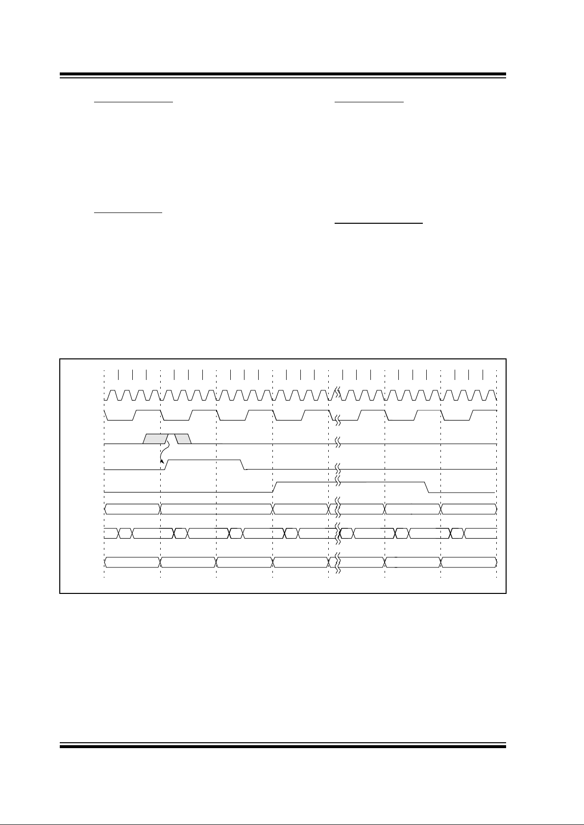
FIGURE 5-5: INT PIN / T0CKI PIN INTERRUPT TIMING
Q2Q1 Q3 Q4 Q2Q1 Q3 Q4 Q2Q1 Q3 Q4 Q2Q1 Q3 Q4 Q2Q1 Q3 Q4 Q2Q1 Q3 Q4 Q2Q1 Q3 Q4
OSC1
OSC2
RA0/INT or
RA1/T0CKI
INTF or
T0CKIF
GLINTD
PC
Instruction
executed
System Bus
Instruction
Fetched
PC PC + 1 Addr (Vector)
PC Inst (PC) Inst (PC+1)
Inst (PC) Dummy Dummy
YY YY + 1
RETFIE
RETFIE
Inst (PC+1)
Inst (Vector)
Addr
Addr
Addr
Addr Addr
Inst (YY + 1)
Dummy
PC + 1

1996 Microchip Technology Inc. DS30412C-page 27
PIC17C4X
5.9 Conte
xt Saving During Interrupts
During an interrupt, only the returned PC value is saved
on the stack. Typically, users may wish to save key registers during an interrupt; e.g. WREG, ALUSTA and the
BSR registers. This requires implementation in software.
Example 5-1 shows the saving and restoring of information for an interrupt service routine. The PUSH and
POP routines could either be in each interrupt service
routine or could be subroutines that were called.
Depending on the application, other registers may also
need to be saved, such as PCLATH.
EXAMPLE 5-1: SAVING STATUS AND WREG IN RAM
;
; The addresses that are used to store the CPUSTA and WREG values
; must be in the data memory address range of 18h - 1Fh. Up to
; 8 locations can be saved and restored using
; the MOVFP instruction. This instruction neither affects the status
; bits, nor corrupts the WREG register.
;
;
PUSH MOVFP WREG, TEMP_W ; Save WREG
MOVFP ALUSTA, TEMP_STATUS ; Save ALUSTA
MOVFP BSR, TEMP_BSR ; Save BSR
ISR : ; This is the interrupt service routine
:
POP MOVFP TEMP_W, WREG ; Restore WREG
MOVFP TEMP_STATUS, ALUSTA ; Restore ALUSTA
MOVFP TEMP_BSR, BSR ; Restore BSR
RETFIE ; Return from Interrupts enabled

PIC17C4X
DS30412C-page 28
1996 Microchip Technology Inc.
NOTES:
1996 Microchip Technology Inc. DS30412C-page 29
PIC17C4X
6.0 MEMORY ORGANIZATION
There are two memory blocks in the PIC17C4X; program memory and data memory. Each block has its
own bus, so that access to each bloc k can occur during
the same oscillator cycle.
The data memory can further be broken down into General Purpose RAM and the Special Function Registers
(SFRs). The operation of the SFRs that control the
“core” are described here. The SFRs used to control
the peripheral modules are described in the section discussing each individual peripheral module.
6.1 Pr
ogram Memory Organization
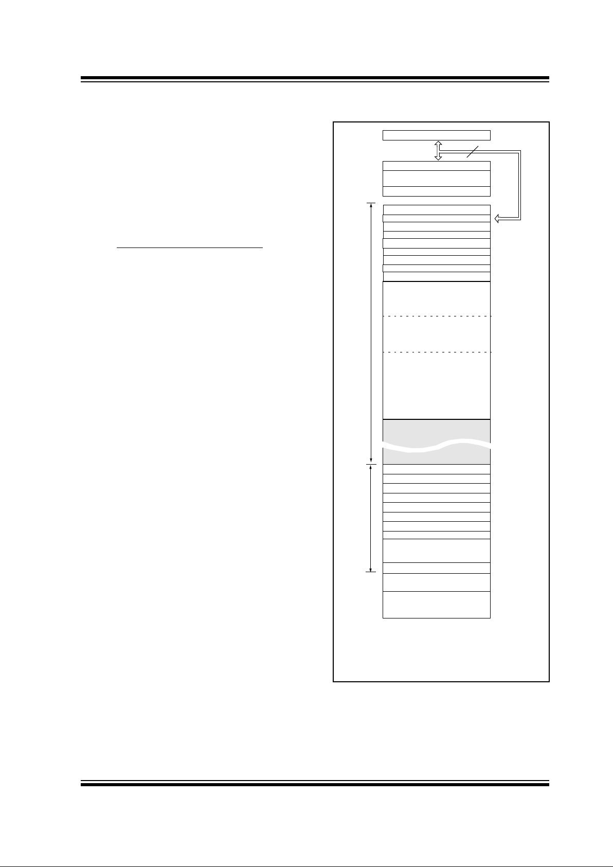
PIC17C4X devices have a 16-bit program counter
capable of addressing a 64K x 16 program memory
space. The reset vector is at 0000h and the interrupt
vectors are at 0008h, 0010h, 0018h, and 0020h
(Figure 6-1).
6.1.1 PROGRAM MEMORY OPERATION
The PIC17C4X can operate in one of four possible pro-
gram memory configurations. The configuration is
selected by two configuration bits. The possible modes
are:
• Microprocessor
• Microcontroller
• Extended Microcontroller
• Protected Microcontroller
The microcontroller and protected microcontroller
modes only allow internal execution. Any access
beyond the program memory reads unknown data.
The protected microcontroller mode also enables the
code protection feature.
The extended microcontroller mode accesses both the
internal program memory as well as external program
memory. Execution automatically switches between
internal and external memory. The 16-bits of address
allow a program memory range of 64K-words.
The microprocessor mode only accesses the external
program memory. The on-chip program memory is
ignored. The 16-bits of address allow a program memory range of 64K-words. Microprocessor mode is the
default mode of an unprogrammed device.
The different modes allow different access to the configuration bits, test memory, and boot ROM. Table 6-1
lists which modes can access which areas in memory.
Test Memory and Boot Memory are not required for
normal operation of the device. Care should be taken to
ensure that no unintended branches occur to these
areas.
FIGURE 6-1: PROGRAM MEMORY MAP
AND STACK
PC<15:0>
Stack Level 1
•
Stack Level 16
Reset Vector
INT Pin Interrupt Vector
Timer0 Interrupt Vector
T0CKI Pin Interrupt Vector
Peripheral Interrupt Vector
FOSC0
FOSC1
WDTPS0
WDTPS1
PM0
Reserved
PM1
Reserved
•
•
Configuration Memory
Space
User Memory
Space
(1)
CALL, RETURN
RETFIE, RETLW
16
0000h
0008h
0010h
0020h
0021h
0018h
7FFh
FDFFh
FE00h
FE01h
FE02h
FE03h
FE04h
FE05h
FE06h
FE07h
FE0Fh
Test EPROM
Boot ROM
FE10h
FF5Fh
FF60h
FFFFh
FFFh
1FFFh
(PIC17C42,
(PIC17C43
(PIC17C44)
Reserved
PM2
(2)
FE08h
PIC17CR42,
PIC17C42A)
PIC17CR43)
Note 1: User memory space may be internal, external, or
both. The memory configuration depends on the
processor mode.
2: This location is reserved on the PIC17C42.
FE0Eh
PIC17C4X
DS30412C-page 30
1996 Microchip Technology Inc.
TABLE 6-1: MODE MEMORY ACCESS
Operating
Mode
Internal
Program
Memory
Configuration Bits,
Test Memory,
Boot ROM
Microprocessor No Access No Access
Microcontroller Access Access
Extended
Microcontroller
Access No Access
Protected
Microcontroller
Access Access
The PIC17C4X can operate in modes where the program memory is off-chip. They are the microprocessor
and extended microcontroller modes. The microprocessor mode is the default for an unprogrammed
device.
Regardless of the processor mode, data memory is
always on-chip.
FIGURE 6-2: MEMORY MAP IN DIFFERENT MODES
Microprocessor
Mode
0000h
FFFFh
External
Program
Memory
External
Program
Memory
0800h
FFFFh
0000h
07FFh
On-chip
Program
Memory
Extended
Microcontroller
Mode
Microcontroller
Modes
0000h
07FFh
0800h
FE00h
FFFFh
OFF-CHIP ON-CHIP OFF-CHIP ON-CHIP OFF-CHIP ON-CHIP
00h
FFh
00h
FFh
00h
FFh
OFF-CHIP ON-CHIP OFF-CHIP ON-CHIP OFF-CHIP ON-CHIP
PROGRAM SPACEDATA SPACE
Config. Bits
Test Memory
Boot ROM
PIC17C42,
0000h
FFFFh
External
Program
Memory
External
Program
Memory
1000h/
FFFFh
0000h
0000h
0FFFh/1FFFh
1000h/2000h
FE00h
FFFFh
OFF-CHIP ON-CHIP OFF-CHIP ON-CHIP OFF-CHIP ON-CHIP
Config. Bits
Test Memory
Boot ROM
PROGRAM SPACEDATA SPACE
00h
FFh 1FFh
120h
OFF-CHIP ON-CHIP
00h
FFh 1FFh
120h
OFF-CHIP ON-CHIP
00h
FFh 1FFh
120h
OFF-CHIP ON-CHIP
0FFFh/1FFFh
2000h
PIC17CR42,
PIC17C42A
PIC17C43,
PIC17CR43,
PIC17C44
On-chip
Program
Memory
On-chip
Program
Memory
On-chip
Program
Memory
 Loading...