

Microchip Technology Inc PIC16HV540-04I-P, PIC16HV540-04I-SO, PIC16HV540-20I-P, PIC16HV540-20I-SO, PIC16HV540-20I-SS Datasheet
...
1998 Microchip Technology Inc.
Preliminary
DS40197A-page 1
PIC16HV540
High-Performance RISC CPU:
• Only 33 single word instructions to learn
• All instructions are single cycle (200 ns) except for
program branches which are two-cycle
• Operating speed: DC - 20 MHz clock input
DC - 200 ns instruction cycle
• 12-bit wide instructions
• 8-bit wide data path
• Seven special function hardware registers
• Four-level deep hardware stack
• Direct, indirect and relative addressing modes for
data and instructions
Peripheral Features:
• 8-bit real time clock/counter (TMR0) with 8-bit
programmable prescaler
• Power-On Reset (POR)
• Brown-Out Protection
• Device Reset Timer (DRT) with short
RC-oscillator start up time
• Programmable Watchdog Timer (WDT) with its
own on-chip RC oscillator for reliable operation
• Sleep Timer
• 8 High Voltage I/O
• 4 Regulated I/O
• Wake up from SLEEP on pin change
• Programmable code-protection
• Power saving SLEEP mode
• Selectable oscillator options:
- RC: Low-cost RC oscillator
- XT: Standard crystal/resonator
- HS: High speed crystal/resonator
- LP: Power saving, low frequency crystal
• Glitch filtering on MCLR
and pin change inputs
= Enhanced Features
Device Pins I/O EPROM RAM
PIC16HV540 18 12 512 25
CMOS Tec hnology:
• Selectable on-chip 3V/5V Regulator
• Low-power, high-speed CMOS EPROM
technology
• Fully static design
• Wide-operating voltage range:
- 3.5V to 15V
• Temperature range:
- Commercial: 0°C to 70°C
- Industrial: -40°C to 85°C
• Low-power consumption
- < 2 mA typical @ 5V, 4 MHz
- 15 µA typical @ 3V, 32 kHz
- < 4.5 µA typical standby current @ 15V (with
WDT disabled), 0°C to 70°C
Enhanced PIC16C54 EPROM-Based 8-Bit CMOS Microcontroller
With On-Chip Voltage Regulator
Pin Configurations
PDIP, SOIC, Windowed CERDIP
18
17
16
15
14
13
12
11
10
• 1
2
3
4
5
6
7
8
9
RA2
RA3
T0CKI
MCLR/VPP
VSS
RB0
RB1
RB2
RB3
RA1
RA0
OSC1/CLKIN
OSC2/CLKOUT
VDD
RB7
RB6
RB5
RB4
PIC16HV540
RA1
RA0
OSC1/CLKIN
OSC2/CLKOUT
V
DD
VDD
RB7
RB6
RB5
RB4
RA2
RA3
T0CKI
MCLR
/VPP
VSS
VSS
RB0
RB1
RB2
RB3
•1
2
3
4
5
6
7
8
9
10
20
19
18
17
16
15
14
13
12
11
SSOP
PIC16HV540
✯
✯
✯
✯
✯
✯
✯
✯
✯

PIC16HV540
DS40197A-page 2
Preliminary
1998 Microchip Technology Inc.
1.0 GENERAL DESCRIPTION
The PIC16HV540 from Microchip Technology is a
low-cost, high-performance, 8-bit, fully-static,
EPROM-based CMOS microcontroller. It is pin and software compatible with the PIC16C5X family of devices. It
employs a RISC architecture with only 33 single word/single cycle instructions. All instructions are single cycle
except for program branches which take two cycles. The
PIC16HV540 delivers performance an order of magnitude
higher than its competitors in the same price category. The
12-bit wide instructions are highly orthogonal resulting in
2:1 code compression over other 8-bit microcontrollers in
its class. The easy-to-use and easy-to-remember instruction set reduces development time significantly.
The PIC16HV540 is the first One-Time-Programmable
(OTP) microcontroller with an on-chip 3 Volt and 5 V olt regulator. This eliminates the need for an external regulator in
many applications powered from 9 Volt or 12 Volt batteries
or unregulated 6 Volt, 9 V olt or 12 Volt mains adapters. The
PIC16HV540 is ideally suited for applications that require
very low standby current at high voltages. These typically
require expensive low current regulators .
The PIC16HV540 is equipped with special features that
reduce system cost and power requirements. The
Power-On Reset (POR) and Device Reset Timer (DRT)
eliminate the need for external reset circuitry . There are f our
oscillator configurations to choose from, including the
power-saving LP (Low Power) oscillator, cost saving RC
oscillator, and XT and HS f or crystal oscillators. Power saving SLEEP mode, Watchdog Timer and code protection
features improve system cost, po wer and reliability.
The UV erasable CERDIP packaged versions are ideal for
code development, while the cost-eff ective OTP v ersions are
suitable for production in any v olume. The customer can take
full advantage of Microchip’s price leadership in O TP microcontrollers while benefiting from the OTP’ s fle xibility.
The PIC16HV540 will in future be supported by a
full-featured macro assembler, a software simulator, an
in-circuit emulator, a ‘C’ compiler, fuzzy logic support
tools, a low-cost dev elopment programmer , and a full f eatured programmer. All the tools are suppor ted on IBM
PC and compatible machines. Functions that correspond
to the PIC16C54 (such as assembly and programming)
can utilize existing tools.
1.1 Applications
The PIC16HV540 fits perfectly in low-power battery applications such as CO and smoke detection, toys, games,
security systems and automobile modules. The EPROM
technology makes customizing of application programs
(transmitter codes, receiver frequencies, etc.) extremely
fast and convenient. The small footprint package, for
through hole or surface mounting, make this microcontroller perfect for applications with space limitations.
Low-cost, low-power, high-performance, ease of use and
I/O flexibility make the PIC16HV540 very versatile e ven in
areas where no microcontroller use has been considered
before (e.g., timer functions, replacement of “glue” logic in
larger systems, coprocessor applications).
1.2 Enhanced Features
1.2.1 REGULATED I/O PORTA INDEPENDENT
OF CORE REGULATOR
PORTA I/O pads and OSC2 output are powered by the
regulated internal voltage VIO. A maximum of 10mA per
output is allowed, or a total of 40mA. The core itself is
powered from the independently regulated supply
V
REG
.
1.2.2 HIGH VOLTAGE I/O PORTB
All eight PORTB I/Os are high voltage I/O. The inputs
will tolerate input voltages as high as the VDD and outputs will swing from VSS to the VDD. The input threshold
voltages vary with supply voltage. (See DC characteristics.)
1.2.3 WAKE UP ON PIN CHANGE ON PORTB [0:3]
Four of the PORTB inputs latch the status of the pin at
the onset of sleep mode. A level change on the inputs
resets the device, implementing wak e up on pin change
(via warm reset). The PC bit in the status register is
reset to indicate that a pin change caused the reset
condition. Any pin change (glitch insensitive) of the
opposite level of the initial value wakes up the device.
This option can be enabled/disabled in OPTION2 register. (See OPTION2 register, Figure 4-3.)
1.2.4 WAKE UP ON PIN CHANGE WITH A
SLOWLY-RISING VOLTAGE ON PORTB [7]
PORTB [7] also implements wake up from sleep, however this input is specifically adapted so that a slowly
rising
voltage does not cause excessive power consumption. This input can be used with external RC circuits for long sleep periods without using the internal
timer and prescaler. This option is also enabled/disabled in OPTION2 register. (The enable/disable bit is
shared with the other 4 wake up inputs.) The ne w w ake
up status bit in the status register is also shared with
the other four wake up inputs.
1.2.5 LOW-VOLTAGE (BROWN-OUT)
DETECTION
A low voltage (Brown-out) detect circuit optionally
resets the device at a voltage level higher than that at
which Brown-out events occur. The nominal trip voltages are 3.1 Volt (for 5 Volt operation) and 2.2 Volt (for
3 Volt operation), respectively. The core remains in the
reset state as long as this condition holds (as if a MCLR
external reset was given). The Brown-out trip level is
user selectable, with built-in interlocks. The Brown-out
detector is disabled at power-up and is activated by
clearing the appropriate bit (BE) in OPTION2 register.
1.2.6 INCREASED STACK DEPTH
The stack depth is 4 levels to allow modular program
implementation by using functions and subroutines.
1998 Microchip Technology Inc.
Preliminary
DS40197A-page 3
PIC16HV540
1.2.7 ENHANCED WATCHDOG TIMER (WDT)
OPERATION
The WDT is enabled b y setting FUSE 2 in the configuration
word. The WDT setting is latched and the fuse disabled
during SLEEP mode to reduce current consumption.
If the WDT is disabled by FUSE 2, it can be enabled/disabled under program control using bit 4 in OPTION2
(SWE). The software WDT control is disab led at power-up .
The current consumption of the on-chip oscillator (used
for the watchdog, oscillator startup timer and sleep
timer) is less than 1µA (typical) at 3 Volt operation.
1.2.8 REDUCED EXTERNAL RC OSCILLATOR
STARTUP TIME
If the RC oscillator option is selected in the Configuration word (FOSC1=1 and FOSCO=1) the oscillator
startup time is 1.0 ms nominal instead of 18 ms nominal. This is applicable after power-up (POR), either
WDT interrupt or wake-up, external reset on MCLR
,
WPC (wake on pin change) and Brown-out.
1.2.9 LOW-VOLTAGE OPERATION OF THE
ENTIRE CPU DURING SLEEP
The voltage regulator can automatically lower the voltage to the core from 5 Volt to 3 V olt during sleep, resulting in reduced current consumption. This is an option
bit in OPTION2 register.
1.2.10 GLITCH FILTERS ON WAKEUP PINS AND
MCLR
Glitch sensitive inputs for wak eup on pin change are filtered to reduce susceptibility to interference. A similar
filter reduces false reset on MCLR.
1.2.11 PROGRAMMABLE CLOCK GENERATOR
When used in RC mode the CLKOUT pin can be used
as a programmable clock output. The output is connected to TMR0, bit 0 and by setting the prescaler,
clock out frequencies of CLKIN/8 to CLKIN/1024 can
be generated. The CLKOUT pin can also be used as a
general purpose output by modifying to TMR0, bit 0.
TABLE 1-1: PIC16HV540 DEVICE
PIC16HV540
Clock
Maximum Frequency (MHz) 20
Memory
EPROM Program Memory 512
RAM Data Memory (bytes) 25
Peripherals
Timer Module(s) TMR0
Packages
I/O Pins 12
Voltage Range (Volts) 3.5V-15V
Number of Instructions 33
Packages 18-pin DIP
SOIC
20-pin SSOP
All PICmicro
devices have Power-on Reset, selectable
WDT, selectable code protect and high I/O current capability.
2.0 PIC16HV540 DEVICE
VARIETIES
A variety of frequency ranges and packaging options
are available. When placing orders, please use the
PIC16HV540 Product Identification System at the back
of this data sheet to specify the correct part number.
2.1 UV Erasab
le Devices
The UV erasable versions, offered in CERDIP packages, are optimal for prototype development and pilot
programs.
UV erasable devices can be progr ammed for an y of the
four oscillator configurations. Microchip's PICSTART
and PRO MATE programmers both support programming of the PIC16HV540. Third party programmers
also are available; refer to Literature Number DS00104
for a list of sources.
2.2 One-Time-Pr
ogrammable (OTP)
Devices
The availability of OTP devices is especially useful for
customers expecting frequent code changes and
updates.
The OTP devices, packaged in plastic packages, permit the user to program them once. In addition to the
program memory, the configuration bits must be programmed.
2.3 Quic
k-Turnaround-Production (QTP)
Devices
Microchip offers a QTP Programming Service for factory production orders. This ser vice is made available
for users who choose not to program a medium to high
quantity of units and whose code patterns have stabilized. The devices are identical to the OTP devices but
with all EPROM locations and configuration bit options
already programmed by the factory. Certain code and
prototype verification procedures apply before production shipments are available. Please contact your
Microchip Technology sales office for more details.
2.4 Serializ
ed
Quick-Turnaround-Production
(SQTP) Devices
Microchip offers the unique programming service where
a few user-defined locations in each device are programmed with different serial numbers. The serial numbers may be random, pseudo-random or sequential.
Serial programming allows each device to have a
unique number which can serve as an entry code,
password or ID number.
PIC16HV540
DS40197A-page 4
Preliminary
1998 Microchip Technology Inc.
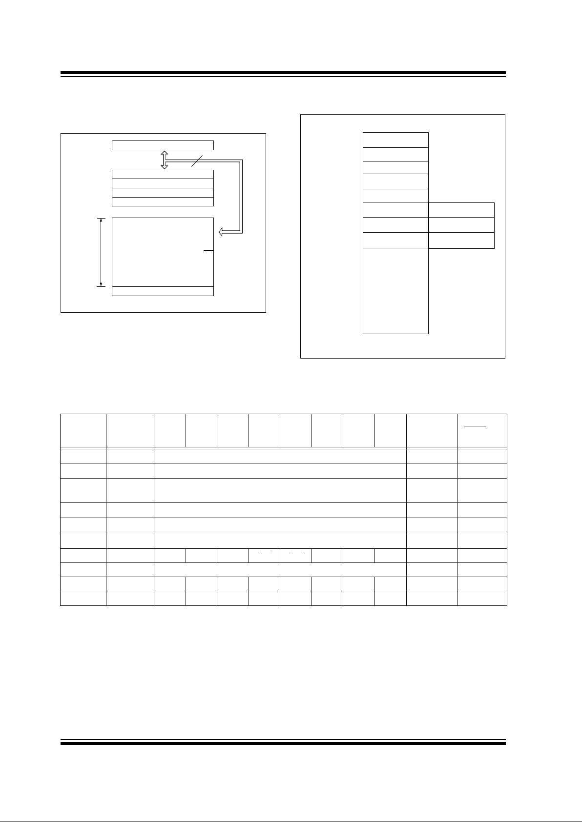
3.0 ARCHITECTURAL OVERVIEW
FIGURE 3-1: PIC16HV540 BLOCK DIAGRAM
This section provides information on the architecture of the PIC16HV540. For information on operation of the peripherals, electrical specifications, etc., please refer to the PIC16C5X data sheet (DS30453).
WDT
TIME
OUT
8
ST ACK 1
EPROM
512 X 12
INSTRUCTION
REGISTER
INSTRUCTION
DECODER
WA TCH-
DOG
CONFIGURA TION W ORD
OSCILLA T OR/
TIMING &
CONTROL
GENERAL
PURPOSE
REGISTER
FILE
(SRAM)
25 Bytes
WDT/TMR0
PRESCALER
OPTION
“OPTION”
“SLEEP”
“CODE
PROTECT”
“OSC
SELECT”
DIRECT ADDRESS
TMR0
FROM W
FROM W
“TRIS 5”
“TRIS 6”
FSR
TRISA PORTA
TRISB PORT
T0CKI
PIN
9-11
9-11
12
12
8
W
4
4
4
DATA BUS
8
8
8
8
ALU
STATUS
FROM W
CLKOUT
8
9
6
5
5-7
OSC1 OSC2 MCLR
LITERALS
PC
“DISABLE”
2
RA3:RA0
RB7:RB0
DIRECT RAM
ADDRESS
8
HIGH VOLTAGE
TRANSLA TION
VREG
3V/5V
Regulator
VDD
ST ACK 2
ST ACK 3
ST ACK 4
“TRIS 7”
FROM W
6
OPTION2
3V/5V
Regulator
BOD
BL/BE
RL/SL
VIO
PC
(PIN CHANGE)
WPC
4
RB3 : RB0
FILTER
RB7
SWE (OPTION2 REGISTER)
1998 Microchip Technology Inc.
Preliminary
DS40197A-page 5
PIC16HV540
TABLE 3-1: PINOUT DESCRIPTION - PIC16HV540
Name
DIP, SOIC
No.
SSOP
No.
I/O/P
Type
Input
Levels
Description
RA0
RA1
RA2
RA3
17
18
1
2
19
20
1
2
I/O
I/O
I/O
I/O
TTL
TTL
TTL
TTL
Independently regulated Bi-directional I/O port — V
IO
RB0
RB1
RB2
RB3
RB4
RB5
RB6
RB7
6
7
8
9
10
11
12
13
7
8
9
10
11
12
13
14
I/O
I/O
I/O
I/O
I/O
I/O
I/O
I/O
TTL
TTL
TTL
TTL
TTL
TTL
TTL
TTL
High-voltage Bi-directional I/O port.
Sourced from V
DD
.
T0CKI 3 3 I ST Clock input to Timer 0. Must be tied to VSS or V
DD,
if not in
use, to reduce current consumption.
MCLR/
V
PP
4 4 I ST Master clear (reset) input/programming voltage input. This
pin is an active low reset to the device. Voltage on the
MCLR
/V
PP
pin must not exceed VDD to avoid unintended
entering of programming mode.
OSC1/CLKIN 16 18 I ST Oscillator crystal input/external clock source input.
OSC2/CLKOUT 15 17 O — Oscillator crystal output. Connects to crystal or resonator in
crystal oscillator mode. In RC mode, OSC2 pin outputs
CLKOUT which has 1/4 the frequency of OSC1, and denotes
the instruction cycle rate.
V
DD
14 15,16 P — Positive supply.
V
SS
5 5,6 P — Ground reference.
Legend: I = input, O = output, I/O = input/output,
P = power, — = Not Used, TTL = TTL input,
ST = Schmitt Trigger input
Wake up on
pin change.
Wake up on SLOW
rising pin change.
PIC16HV540
DS40197A-page 6
Preliminary
1998 Microchip Technology Inc.
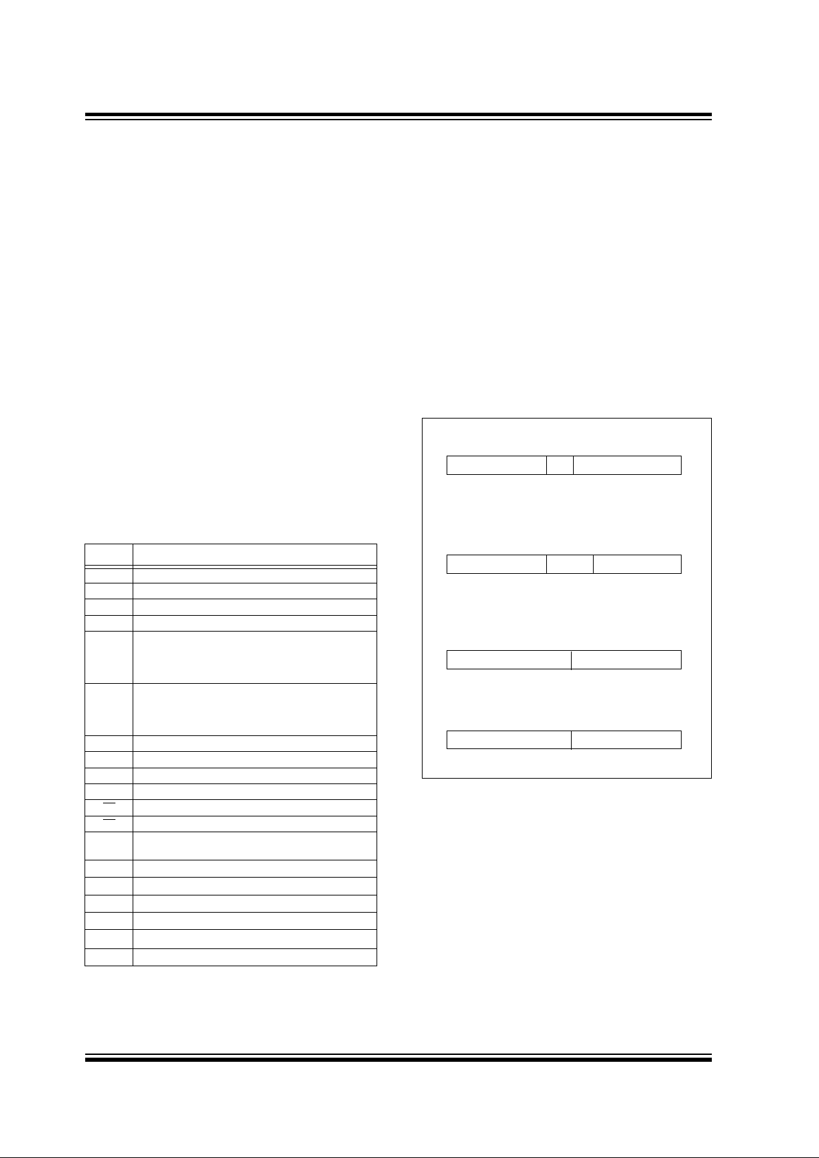
4.0 MEMORY ORGANIZATION
FIGURE 4-1: PIC16HV540 PROGRAM
MEMORY MAP AND STACK
PC<8:0>
Stack Level 1
Stack Level 2
User Memory
Space
CALL, RETLW
9
000h
1FFh
Reset Vector
0FFh
100h
On-chip
Program
Memory
Stack Level 3
Stack Level 4
FIGURE 4-2: PIC16HV540 REGISTER FILE
MAP
File Address
00h
01h
02h
03h
04h
05h
06h
07h
1Fh
INDF
(1)
TMR0
PCL
STATUS
FSR
PORTA
PORTB
General
Purpose
Registers
Note 1: Not a physical register.
0Fh
10h
08h
TRISA
TRISB
OPTION2
TABLE 4-1: SPECIAL FUNCTION REGISTER SUMMARY
Address Name Bit 7 Bit 6 Bit 5 Bit 4 Bit 3 Bit 2 Bit 1 Bit 0
Value on
Power-On
Reset
Value on
MCLR
and
WDT Reset
N/A TRIS I/O control registers (TRISA, TRISB)
1111 1111 1111 1111
N/A OPTION Contains control bits to configure Timer0 and Timer0/WDT prescaler
--11 1111 --11 1111
N/A OPTION2 Contains control bits to configure pin changes, software enabled WDT,
xx11 1111 xx11 1111
regulation and brown-out
00h INDF Uses contents of FSR to address data memory (not a physical register)
xxxx xxxx uuuu uuuu
01h TMR0 8-bit real-time clock/counter
xxxx xxxx uuuu uuuu
02h
(1)
PCL Low order 8 bits of PC
1111 1111 1111 1111
03h STATUS PCF PA1 PA0 T
O PD ZDCC
1001 1xxx 100q quuu
04h FSR Indirect data memory address pointer
1xxx xxxx 1uuu uuuu
05h PORTA ————RA3RA2RA1RA0
---- xxxx ---- uuuu
06h PORTB RB7 RB6 RB5 RB4 RB3 RB2 RB1 RB0
xxxx xxxx uuuu uuuu
Legend: Shaded boxes = unimplemented or unused, – = unimplemented, read as '0' (if applicable)
x
= unknown, u = unchanged, q = value depends on condition.
Note 1: The upper b yte of the Program Counter is not directly accessib le . See Section 4.5 of the PIC16C5X data sheet (DS30453)
for an explanation of how to access these bits.
2: File address 07h is a general purpose register on the PIC16HV540.
3: PCF This bit is set to 1 after power up-reset (POR) or sleep command.
4: PCF This bit is set to 0 after a wake up on pin change event.

1998 Microchip Technology Inc.
Preliminary
DS40197A-page 7
PIC16HV540
Figure 4-3: OPTION2 REGISTER (TRIS 07h)
U-0 U-0 W-1 W-1 W-1 W-1 W-1 W-1
- - WPC SWE RL SL BL BE W = Writable bit
U = Unimplemented bit
-n = Value at POR reset
bit7 6 5 4 3 2 1 0
bit 7-6:
Unimplemented.
bit 5:
WPC
: Wake up on pin change
1 = Disabled
0 = Enabled
bit 4:
SWE
: Software WDT enable
1 = Disabled
0 = Enabled
bit 3:
RL
: Regulated voltage level select bit
1 = 5 Volt
0 = 3 Volt
bit 2:
SL
: Sleep voltage level select bit
1 = RL bit setting
0 = 3 Volt
bit 1:
BL
: Brown-out voltage level select bit
1 = RL bit setting, but SL during sleep
0 = 3 Volt
bit 0:
BE
: Brown-out enabled
1 = Disabled
0 = Enabled
PIC16HV540
DS40197A-page 8
Preliminary
1998 Microchip Technology Inc.
5.0 INSTRUCTION SET SUMMARY
Each PIC16HV540 instruction is a 12-bit word divided into
an OPCODE, which specifies the instruction type, and one
or more operands which further specify the operation of
the instruction. The PIC16HV540 instruction set summary
in Table 5-2 groups the instructions into byte-oriented,
bit-oriented, and literal and control operations. Table 5-1
shows the opcode field descriptions.
For
byte-oriented
instructions, 'f' represents a file register
designator and 'd' represents a destination designator. The
file register designator is used to specify which one of the
32 file registers is to be used by the instruction.
The destination designator specifies where the result
of the operation is to be placed. If 'd' is '0', the result is
placed in the W register. If 'd' is '1', the result is placed
in the file register specified in the instruction.
For
bit-oriented
instructions, 'b' represents a bit field
designator which selects the number of the bit affected
by the operation, while 'f' represents the number of the
file in which the bit is located.
For
literal and control
operations, 'k' represents an
8 or 9-bit constant or literal value.
TABLE 5-1: OPCODE FIELD
DESCRIPTIONS
Field Description
f
Register file address (0x00 to 0x7F)
W
Working register (accumulator)
b
Bit address within an 8-bit file register
k
Literal field, constant data or label
x
Don't care location (= 0 or 1)
The assembler will generate code with x = 0. It is
the recommended form of use for compatibility
with all Microchip software tools.
d
Destination select;
d = 0 (store result in W)
d = 1 (store result in file register 'f')
Default is d = 1
label
Label name
TOS
Top of Stack
PC Program Counter
WDT Watchdog Timer Counter
TO
Time-Out bit
PD Power-Down bit
dest
Destination, either the W register or the specified
register file location
[ ]
Options
( )
Contents
→
Assigned to
< >
Register bit field
∈
In the set of
i
talics
User defined term (font is courier)
All instructions are executed within one single
instruction cycle, unless a conditional test is true or the
program counter is changed as a result of an
instruction. In this case, the execution takes two
instruction cycles. One instruction cycle consists of
four oscillator periods. Thus, for an oscillator frequency
of 4 MHz, the normal instruction execution time is 1 µs.
If a conditional test is true or the program counter is
changed as a result of an instruction, the instruction
execution time is 2 µs.
Figure 5-1 shows the three general formats that the
instructions can have. All examples in the figure use the
following format to represent a hexadecimal number:
0xhhh
where 'h' signifies a hexadecimal digit.
FIGURE 5-1: GENERAL FORMAT FOR
INSTRUCTIONS
Byte-oriented file register operations
11 6 5 4 0
d = 0 for destination W
OPCODE d f (FILE #)
d = 1 for destination f
f = 5-bit file register address
Bit-oriented file register operations
11 8 7 5 4 0
OPCODE b (BIT #) f (FILE #)
b = 3-bit bit address
f = 5-bit file register address
Literal and control operations (except GOTO)
11 8 7 0
OPCODE k (literal)
k = 8-bit immediate value
Literal and control operations - GOTO instruction
11 9 8 0
OPCODE k (literal)
k = 9-bit immediate value

1998 Microchip Technology Inc. Preliminary DS40197A-page 9
PIC16HV540
TABLE 5-2: INSTRUCTION SET SUMMARY
Mnemonic,
Operands Description Cycles
12-Bit Opcode
Status
Affected NotesMSb LSb
ADDWF
ANDWF
CLRF
CLRW
COMF
DECF
DECFSZ
INCF
INCFSZ
IORWF
MOVF
MOVWF
NOP
RLF
RRF
SUBWF
SWAPF
XORWF
f,d
f,d
f
–
f, d
f, d
f, d
f, d
f, d
f, d
f, d
f
–
f, d
f, d
f, d
f, d
f, d
Add W and f
AND W with f
Clear f
Clear W
Complement f
Decrement f
Decrement f, Skip if 0
Increment f
Increment f, Skip if 0
Inclusive OR W with f
Move f
Move W to f
No Operation
Rotate left f through Carry
Rotate right f through Carry
Subtract W from f
Swap f
Exclusive OR W with f
1
1
1
1
1
1
1(2)
1
1(2)
1
1
1
1
1
1
1
1
1
0001
0001
0000
0000
0010
0000
0010
0010
0011
0001
0010
0000
0000
0011
0011
0000
0011
0001
11df
01df
011f
0100
01df
11df
11df
10df
11df
00df
00df
001f
0000
01df
00df
10df
10df
10df
ffff
ffff
ffff
0000
ffff
ffff
ffff
ffff
ffff
ffff
ffff
ffff
0000
ffff
ffff
ffff
ffff
ffff
C,DC,Z
Z
Z
Z
Z
Z
None
Z
None
Z
Z
None
None
C
C
C,DC,Z
None
Z
1,2,4
2,4
4
2,4
2,4
2,4
2,4
2,4
2,4
1,4
2,4
2,4
1,2,4
2,4
2,4
BIT-ORIENTED FILE REGISTER OPERATIONS
BCF
BSF
BTFSC
BTFSS
f, b
f, b
f, b
f, b
Bit Clear f
Bit Set f
Bit Test f, Skip if Clear
Bit Test f, Skip if Set
1
1
1 (2)
1 (2)
0100
0101
0110
0111
bbbf
bbbf
bbbf
bbbf
ffff
ffff
ffff
ffff
None
None
None
None
2,4
2,4
LITERAL AND CONTROL OPERATIONS
ANDLW
CALL
CLRWDT
GOTO
IORLW
MOVLW
OPTION
RETLW
SLEEP
TRIS
XORLW
k
k
k
k
k
k
k
k
–
f
k
AND literal with W
Call subroutine
Clear Watchdog Timer
Unconditional branch
Inclusive OR Literal with W
Move Literal to W
Load OPTION register
Return, place Literal in W
Go into standby mode
Load TRIS register
Exclusive OR Literal to W
1
2
1
2
1
1
1
2
1
1
1
1110
1001
0000
101k
1101
1100
0000
1000
0000
0000
1111
kkkk
kkkk
0000
kkkk
kkkk
kkkk
0000
kkkk
0000
0000
kkkk
kkkk
kkkk
0100
kkkk
kkkk
kkkk
0010
kkkk
0011
0fff
kkkk
Z
None
T
O, PD
None
Z
None
None
None
T
O, PD
None
Z
1
3
Note 1: The 9th bit of the program counter will be forced to a '0' by any instruction that writes to the PC except for GOTO.
(See individual device data sheets, Memory Section/Indirect Data Addressing, INDF and FSR Registers)
2: When an I/O register is modified as a function of itself (e.g. MOVF PORTB, 1), the value used will be that value
present on the pins themselves. For example, if the data latch is '1' for a pin configured as input and is driven
low by an external device , the data will be written back with a '0'.
3: The instruction TRIS f, where f = 5 or 6 causes the contents of the W register to be written to the tristate
latches of PORTA or B respectively . A '1' forces the pin to a hi-impedance state and disables the output buffers .
4: If this instruction is executed on the TMR0 register (and, where applicable , d = 1), the prescaler will be cleared
(if assigned to TMR0).

PIC16HV540
DS40197A-page 10 Preliminary 1998 Microchip Technology Inc.
ADDWF Add W and f
Syntax: [
label
] ADDWF f,d
Operands: 0 ≤ f ≤ 31
d ∈ [0,1]
Operation: (W) + (f) → (dest)
Status Affected: C, DC, Z
Encoding:
0001 11df ffff
Description:
Add the contents of the W register and
register 'f'. If 'd' is 0 the result is stored
in the W register . If 'd' is '1' the result is
stored back in register 'f'
.
Words: 1
Cycles: 1
Example:
ADDWF FSR, 0
Before Instruction
W = 0x17
FSR = 0xC2
After Instruction
W = 0xD9
FSR = 0xC2
ANDLW And literal with W
Syntax: [
label
] ANDLW k
Operands: 0 ≤ k ≤ 255
Operation: (W).AND. (k) → (W)
Status Affected: Z
Encoding:
1110 kkkk kkkk
Description:
The contents of the W register are
AND’ed with the eight-bit literal 'k'. The
result is placed in the W register
.
Words: 1
Cycles: 1
Example:
ANDLW 0x5F
Before Instruction
W = 0xA3
After Instruction
W = 0x03
ANDWF AND W with f
Syntax: [
label
] ANDWF f,d
Operands: 0 ≤ f ≤ 31
d ∈ [0,1]
Operation: (W) .AND. (f) → (dest)
Status Affected: Z
Encoding:
0001 01df ffff
Description:
The contents of the W register are
AND’ed with register 'f'. If 'd' is 0 the
result is stored in the W register . If 'd' is
'1' the result is stored back in register 'f'
.
Words: 1
Cycles: 1
Example:
ANDWF FSR, 1
Before Instruction
W = 0x17
FSR = 0xC2
After Instruction
W = 0x17
FSR = 0x02
BCF Bit Clear f
Syntax: [
label
] BCF f,b
Operands: 0 ≤ f ≤ 31
0 ≤ b ≤ 7
Operation: 0 → (f<b>)
Status Affected: None
Encoding:
0100 bbbf ffff
Description:
Bit 'b' in register 'f' is cleared.
Words: 1
Cycles: 1
Example:
BCF FLAG_REG, 7
Before Instruction
FLAG_REG = 0xC7
After Instruction
FLAG_REG = 0x47

1998 Microchip Technology Inc. Preliminary DS40197A-page 11
PIC16HV540
BSF Bit Set f
Syntax: [
label
] BSF f,b
Operands: 0 ≤ f ≤ 31
0 ≤ b ≤ 7
Operation: 1 → (f<b>)
Status Affected: None
Encoding:
0101 bbbf ffff
Description:
Bit 'b' in register 'f' is set.
Words: 1
Cycles: 1
Example:
BSF FLAG_REG, 7
Before Instruction
FLAG_REG = 0x0A
After Instruction
FLAG_REG = 0x8A
BTFSC Bit Test f, Skip if Clear
Syntax: [
label
] BTFSC f,b
Operands: 0 ≤ f ≤ 31
0 ≤ b ≤ 7
Operation: skip if (f<b>) = 0
Status Affected: None
Encoding: 0110
bbbf ffff
Description:
If bit 'b' in register 'f' is 0 then the next
instruction is skipped.
If bit 'b' is 0 then the next instruction
fetched during the current instruction
execution is discarded, and an NOP is
executed instead, making this a 2 cycle
instruction.
Words: 1
Cycles: 1(2)
Example:
HERE
FALSE
TRUE
BTFSC
GOTO
•
•
•
FLAG,1
PROCESS_CODE
Before Instruction
PC = address (HERE)
After Instruction
if FLAG<1> = 0,
PC = address (TRUE);
if FLAG<1> = 1,
PC = address(FALSE)
BTFSS Bit Test f, Skip if Set
Syntax: [
label
] BTFSS f,b
Operands: 0 ≤ f ≤ 31
0 ≤ b < 7
Operation: skip if (f<b>) = 1
Status Affected: None
Encoding:
0111 bbbf ffff
Description:
If bit 'b' in register 'f' is '1' then the next
instruction is skipped.
If bit 'b' is '1', then the next instruction
fetched during the current instruction
execution, is discarded and an NOP is
executed instead, making this a 2 cycle
instruction.
Words: 1
Cycles: 1(2)
Example:
HERE BTFSS FLAG,1
FALSE GOTO PROCESS_CODE
TRUE •
•
•
Before Instruction
PC = address (HERE)
After Instruction
If FLAG<1> = 0,
PC = address (FALSE);
if FLAG<1> = 1,
PC = address (TRUE)

PIC16HV540
DS40197A-page 12 Preliminary 1998 Microchip Technology Inc.
CALL Subroutine Call
Syntax: [
label
] CALL k
Operands: 0 ≤ k ≤ 255
Operation: (PC) + 1→ Top of Stack;
k → PC<7:0>;
(STATUS<6:5>) → PC<10:9>;
0 → PC<8>
Status Affected: None
Encoding:
1001 kkkk kkkk
Description:
Subroutine call. First, return address
(PC+1) is pushed onto the stack. The
eight bit immediate address is loaded
into PC bits <7:0>. The upper bits
PC<10:9> are loaded from STA-
TUS<6:5>, PC<8> is cleared. CALL is
a two cycle instruction.
Words: 1
Cycles: 2
Example:
HERE CALL THERE
Before Instruction
PC = address (HERE)
After Instruction
PC = address (THERE)
TOS= address (HERE + 1)
CLRF Clear f
Syntax: [
label
] CLRF f
Operands: 0 ≤ f ≤ 31
Operation: 00h → (f);
1 → Z
Status Affected: Z
Encoding:
0000 011f ffff
Description:
The contents of register 'f' are cleared
and the Z bit is set.
Words: 1
Cycles: 1
Example:
CLRF FLAG_REG
Before Instruction
FLAG_REG = 0x5A
After Instruction
FLAG_REG = 0x00
Z=1
CLRW Clear W
Syntax: [
label
] CLRW
Operands: None
Operation: 00h → (W);
1 → Z
Status Affected: Z
Encoding:
0000 0100 0000
Description:
The W register is cleared. Zero bit (Z)
is set.
Words: 1
Cycles: 1
Example:
CLRW
Before Instruction
W = 0x5A
After Instruction
W = 0x00
Z=1
CLRWDT Clear Watchdog Timer
Syntax: [
label
] CLRWDT
Operands: None
Operation: 00h → WDT;
0 → WDT prescaler (if assigned);
1 → T
O;
1 → PD
Status Affected: TO, PD
Encoding:
0000 0000 0100
Description:
The CLRWDT instruction resets the
WDT. It also resets the prescaler, if the
prescaler is assigned to the WDT and
not Timer0. Status bits TO and PD are
set.
Words: 1
Cycles: 1
Example:
CLRWDT
Before Instruction
WDT counter = ?
After Instruction
WDT counter = 0x00
WDT prescale = 0
TO =1
PD =1

1998 Microchip Technology Inc. Preliminary DS40197A-page 13
PIC16HV540
COMF Complement f
Syntax: [
label
] COMF f,d
Operands: 0 ≤ f ≤ 31
d ∈ [0,1]
Operation: (f
) → (dest)
Status Affected: Z
Encoding:
0010 01df ffff
Description:
The contents of register 'f' are complemented. If 'd' is 0 the result is stored in
the W register. If 'd' is 1 the result is
stored back in register 'f'.
Words: 1
Cycles: 1
Example:
COMF REG1,0
Before Instruction
REG1 = 0x13
After Instruction
REG1 = 0x13
W = 0xEC
DECF Decrement f
Syntax: [
label
] DECF f,d
Operands: 0 ≤ f ≤ 31
d ∈ [0,1]
Operation: (f) – 1 → (dest)
Status Affected: Z
Encoding:
0000 11df ffff
Description:
Decrement register 'f'. If 'd' is 0 the
result is stored in the W register . If 'd' is
1 the result is stored back in register 'f'.
Words: 1
Cycles: 1
Example:
DECF CNT,
1
Before Instruction
CNT = 0x01
Z=0
After Instruction
CNT = 0x00
Z=1
DECFSZ Decrement f, Skip if 0
Syntax: [
label
] DECFSZ f,d
Operands: 0 ≤ f ≤ 31
d ∈ [0,1]
Operation: (f) – 1 → d; skip if result = 0
Status Affected: None
Encoding:
0010 11df ffff
Description:
The contents of register 'f' are decre-
mented. If 'd' is 0 the result is placed in
the W register. If 'd' is 1 the result is
placed back in register 'f'.
If the result is 0, the next instruction,
which is already fetched, is discarded
and an NOP is executed instead mak-
ing it a two cycle instruction.
Words: 1
Cycles: 1(2)
Example:
HERE DECFSZ CNT, 1
GOTO LOOP
CONTINUE •
•
•
Before Instruction
PC = address (HERE)
After Instruction
CNT = CNT - 1;
if CNT = 0,
PC = address (CONTINUE);
if CNT ≠ 0,
PC = address (HERE+1)
GOTO Unconditional Branch
Syntax: [
label
] GOTO k
Operands: 0 ≤ k ≤ 511
Operation: k → PC<8:0>;
STATUS<6:5> → PC<10:9>
Status Affected: None
Encoding:
101k kkkk kkkk
Description:
GOTO is an unconditional branch. The
9-bit immediate value is loaded into PC
bits <8:0>. The upper bits of PC are
loaded from STATUS<6:5>. GOTO is a
two cycle instruction.
Words: 1
Cycles: 2
Example:
GOTO THERE
After Instruction
PC = address (THERE)

PIC16HV540
DS40197A-page 14 Preliminary 1998 Microchip Technology Inc.
INCF Increment f
Syntax: [
label
] INCF f,d
Operands: 0 ≤ f ≤ 31
d ∈ [0,1]
Operation: (f) + 1 → (dest)
Status Affected: Z
Encoding:
0010 10df ffff
Description:
The contents of register 'f' are incre-
mented. If 'd' is 0 the result is placed in
the W register. If 'd' is 1 the result is
placed back in register 'f'.
Words: 1
Cycles: 1
Example:
INCF CNT,
1
Before Instruction
CNT = 0xFF
Z=0
After Instruction
CNT = 0x00
Z=1
INCFSZ Increment f, Skip if 0
Syntax: [
label
] INCFSZ f,d
Operands: 0 ≤ f ≤ 31
d ∈ [0,1]
Operation: (f) + 1 → (dest), skip if result = 0
Status Affected: None
Encoding:
0011 11df ffff
Description:
The contents of register 'f' are incre-
mented. If 'd' is 0 the result is placed in
the W register. If 'd' is 1 the result is
placed back in register 'f'.
If the result is 0, then the next instruc-
tion, which is already fetched, is dis-
carded and an NOP is executed
instead making it a two cycle instruc-
tion.
Words: 1
Cycles: 1(2)
Example:
HERE INCFSZ CNT, 1
GOTO LOOP
CONTINUE •
•
•
Before Instruction
PC = address (HERE)
After Instruction
CNT = CNT + 1;
if CNT = 0,
PC = address (CONTINUE);
if CNT ≠ 0,
PC = address (HERE +1)
IORLW Inclusive OR literal with W
Syntax: [
label
] IORLW k
Operands: 0 ≤ k ≤ 255
Operation: (W) .OR. (k) → (W)
Status Affected: Z
Encoding:
1101 kkkk kkkk
Description:
The contents of the W register are
OR’ed with the eight bit literal 'k'. The
result is placed in the W register.
Words: 1
Cycles: 1
Example:
IORLW 0x35
Before Instruction
W = 0x9A
After Instruction
W = 0xBF
Z=0
IORWF Inclusive OR W with f
Syntax: [
label
] IORWF f,d
Operands: 0 ≤ f ≤ 31
d ∈ [0,1]
Operation: (W).OR. (f) → (dest)
Status Affected: Z
Encoding:
0001 00df ffff
Description:
Inclusive OR the W register with regis-
ter 'f'. If 'd' is 0 the result is placed in
the W register. If 'd' is 1 the result is
placed back in register 'f'.
Words: 1
Cycles: 1
Example:
IORWF RESULT, 0
Before Instruction
RESULT = 0x13
W = 0x91
After Instruction
RESULT = 0x13
W = 0x93
Z=0

1998 Microchip Technology Inc. Preliminary DS40197A-page 15
PIC16HV540
MOVF Move f
Syntax: [
label
] MOVF f,d
Operands: 0 ≤ f ≤ 31
d ∈ [0,1]
Operation: (f) → (dest)
Status Affected: Z
Encoding:
0010 00df ffff
Description:
The contents of register 'f' is moved to
destination 'd'. If 'd' is 0, destination is
the W register . If 'd' is 1, the destination
is file register 'f'. 'd' is 1 is useful to test
a file register since status flag Z is
affected.
Words: 1
Cycles: 1
Example:
MOVF FSR, 0
After Instruction
W = value in FSR register
MOVLW Move Literal to W
Syntax: [
label
] MOVLW k
Operands: 0 ≤ k ≤ 255
Operation: k → (W)
Status Affected: None
Encoding:
1100 kkkk kkkk
Description:
The eight bit literal 'k' is loaded into the
W register. The don’t cares will assemble as 0s.
Words: 1
Cycles: 1
Example:
MOVLW 0x5A
After Instruction
W = 0x5A
MOVWF Move W to f
Syntax: [
label
] MOVWF f
Operands: 0 ≤ f ≤ 31
Operation: (W) → (f)
Status Affected: None
Encoding:
0000 001f ffff
Description:
Move data from the W register to register 'f'
.
Words: 1
Cycles: 1
Example:
MOVWF TEMP_REG
Before Instruction
TEMP_REG = 0xFF
W = 0x4F
After Instruction
TEMP_REG = 0x4F
W = 0x4F
NOP No Operation
Syntax: [
label
] NOP
Operands: None
Operation: No operation
Status Affected: None
Encoding:
0000 0000 0000
Description: No operation.
Words: 1
Cycles: 1
Example:
NOP

PIC16HV540
DS40197A-page 16 Preliminary 1998 Microchip Technology Inc.
OPTION Load OPTION Register
Syntax: [
label
] OPTION
Operands: None
Operation: (W) → OPTION
Status Affected: None
Encoding:
0000 0000 0010
Description:
The content of the W register is loaded
into the OPTION register.
Words: 1
Cycles: 1
Example
OPTION
Before Instruction
W = 0x07
After Instruction
OPTION = 0x07
RETLW Return with Literal in W
Syntax: [
label
] RETLW k
Operands: 0 ≤ k ≤ 255
Operation: k → (W);
TOS → PC
Status Affected: None
Encoding:
1000 kkkk kkkk
Description:
The W register is loaded with the eight
bit literal 'k'. The program counter is
loaded from the top of the stack (the
return address). This is a two cycle
instruction.
Words: 1
Cycles: 2
Example:
TABLE
CALL TABLE ;W contains
;table offset
;value.
• ;W now has table
• ;value.
•
ADDWF PC ;W = offset
RETLW k1 ;Begin table
RETLW k2 ;
•
•
•
RETLW kn ; End of table
Before Instruction
W = 0x07
After Instruction
W = value of k8
RLF Rotate Left f through Carry
Syntax: [
label
] RLF f,d
Operands: 0 ≤ f ≤ 31
d ∈ [0,1]
Operation: See description below
Status Affected: C
Encoding:
0011 01df ffff
Description:
The contents of register 'f' are rotated
one bit to the left through the Carry
Flag. If 'd' is 0 the result is placed in the
W register. If 'd' is 1 the result is stored
back in register 'f'.
Words: 1
Cycles: 1
Example:
RLF REG1,0
Before Instruction
REG1 = 1110 0110
C=0
After Instruction
REG1 = 1110 0110
W=1100 1100
C=1
RRF Rotate Right f through Carry
Syntax: [
label
] RRF f,d
Operands: 0 ≤ f ≤ 31
d ∈ [0,1]
Operation: See description below
Status Affected: C
Encoding:
0011 00df ffff
Description:
The contents of register 'f' are rotated
one bit to the right through the Carry
Flag. If 'd' is 0 the result is placed in the
W register. If 'd' is 1 the result is placed
back in register 'f'.
Words: 1
Cycles: 1
Example:
RRF REG1,0
Before Instruction
REG1 = 1110 0110
C=0
After Instruction
REG1 = 1110 0110
W=0111 0011
C=0
C
register 'f'
C
register 'f'

1998 Microchip Technology Inc. Preliminary DS40197A-page 17
PIC16HV540
SLEEP Enter SLEEP Mode
Syntax:
[
label
]
SLEEP
Operands: None
Operation: 00h → WDT;
0 → WDT prescaler;
1 → T
O;
0 → PD
Status Affected: TO, PD
Encoding:
0000 0000 0011
Description:
Time-out status bit (TO) is set. The
power down status bit (PD) is cleared.
The WDT and its prescaler are cleared.
The processor is put into SLEEP mode
with the oscillator stopped. See sec-
tion on SLEEP for more details.
Words: 1
Cycles: 1
Example: SLEEP
SUBWF Subtract W from f
Syntax:
[
label
] SUBWF f,d
Operands: 0 ≤ f ≤ 31
d ∈ [0,1]
Operation: (f) – (W) → (dest)
Status Affected: C, DC, Z
Encoding:
0000 10df ffff
Description:
Subtract (2’s complement method) the
W register from register 'f'. If 'd' is 0 the
result is stored in the W register . If 'd' is
1 the result is stored back in register 'f'.
Words: 1
Cycles: 1
Example 1
:
SUBWF REG1, 1
Before Instruction
REG1 = 3
W=2
C=?
After Instruction
REG1 = 1
W=2
C = 1 ; result is positive
Example 2:
Before Instruction
REG1 = 2
W=2
C=?
After Instruction
REG1 = 0
W=2
C = 1 ; result is zero
Example 3:
Before Instruction
REG1 = 1
W=2
C=?
After Instruction
REG1 = FF
W=2
C = 0 ; result is negative

PIC16HV540
DS40197A-page 18 Preliminary 1998 Microchip Technology Inc.
SWAPF Swap Nibbles in f
Syntax: [
label
] SWAPF f,d
Operands: 0 ≤ f ≤ 31
d ∈ [0,1]
Operation: (f<3:0>) → (dest<7:4>);
(f<7:4>) → (dest<3:0>)
Status Affected: None
Encoding:
0011 10df ffff
Description:
The upper and lower nibbles of register
'f' are exchanged. If 'd' is 0 the result is
placed in W register . If 'd' is 1 the result
is placed in register 'f'.
Words: 1
Cycles: 1
Example
SWAPF
REG1, 0
Before Instruction
REG1 = 0xA5
After Instruction
REG1 = 0xA5
W = 0X5A
TRIS Load TRIS Register
Syntax: [
label
] TRIS f
Operands: f = 5, 6 or 7
Operation: (W) → TRIS register f
Status Affected: None
Encoding:
0000 0000 0fff
Description:
TRIS register 'f' (f = 5, 6, or 7) is loaded
with the contents of the W register
Words: 1
Cycles: 1
Example
TRIS PORTA
Before Instruction
W = 0XA5
After Instruction
TRISA = 0XA5
XORLW Exclusive OR literal with W
Syntax:
[
label
] XORLW k
Operands: 0 ≤ k ≤ 255
Operation: (W) .XOR. k → (W)
Status Affected: Z
Encoding:
1111 kkkk kkkk
Description:
The contents of the W register are
XOR’ed with the eight bit literal 'k'. The
result is placed in the W register.
Words: 1
Cycles: 1
Example: XORLW 0xAF
Before Instruction
W = 0xB5
After Instruction
W = 0x1A
XORWF Exclusive OR W with f
Syntax: [
label
] XORWF f,d
Operands: 0 ≤ f ≤ 31
d ∈ [0,1]
Operation: (W) .XOR. (f) → (dest)
Status Affected: Z
Encoding:
0001 10df ffff
Description:
Exclusive OR the contents of the W
register with register 'f'. If 'd' is 0 the
result is stored in the W register . If 'd' is
1 the result is stored back in register 'f'.
Words: 1
Cycles: 1
Example XORWF
REG,1
Before Instruction
REG = 0xAF
W = 0xB5
After Instruction
REG = 0x1A
W = 0xB5

1998 Microchip Technology Inc. Preliminary DS40197A-page 19
PIC16HV540
6.0 PIC16HV540 DEVICE
VARIETIES
A variety of frequency ranges and packaging options
are available. Depending on application and
production requirements, the proper device option can
be selected using the information in this section. When
placing orders, please use the PIC16HV540 Product
Identification System at the back of this data sheet to
specify the correct part number.
For the PIC16HV540 family of devices, there is one
device type, as indicated in the device number:
1. HV, as in PIC16HV540A. Refer to PIC16C5X
data sheet (DS30453A) for an explanation of
how to access these bits. These devices have
EPROM program memory and operate over the
standard voltage range of 3.5 to 13 volts.
6.1 UV Erasable Devices
The UV erasable versions, offered in CERDIP
packages, are optimal for prototype development and
pilot programs
UV erasable devices can be programmed for any of
the four oscillator configurations. Microchip's
PICSTART
and PRO MATE programmers both
support programming of the PIC16HV540. Third party
programmers also are available; refer to the Third
Party Guide for a list of sources.
6.2 One-Time-Programmable (OTP)
Devices
The availability of OTP devices is especially useful for
customers expecting frequent code changes and
updates.
The OTP devices, packaged in plastic packages,
permit the user to program them once. In addition to
the program memory, the configuration bits must be
programmed.
6.3 Quick-Turnaround-Production (QTP)
Devices
Microchip offers a QTP Programming Service for
factory production orders. This service is made
available for users who choose not to program a
medium to high quantity of units and whose code
patterns have stabilized. The devices are identical to
the OTP devices but with all EPROM locations and
configuration bit options already programmed by the
factory. Certain code and prototype verification
procedures apply before production shipments are
available. Please contact your Microchip Technology
sales office for more details.
6.4 Serialized
Quick-Turnaround-Production
(SQTP ) Devices
Microchip offers the unique programming service
where a few user-defined locations in each device are
programmed with different serial numbers. The serial
numbers may be random, pseudo-random or
sequential.
Serial programming allows each device to have a
unique number which can serve as an entry code,
password or ID number.
SM

PIC16HV540
DS40197A-page 20 Preliminary 1998 Microchip Technology Inc.
7.0 ELECTRICAL CHARACTERISTICS - PIC16HV540
Absolute Maximum Ratings
†
Ambient temperature under bias...............................................................................................................-20˚C to +85˚C
Storage temperature ............................................................................................................................. - 65˚C to +150˚C
Voltage on V
DD with respect to VSS................................................................................................................... 0 to +16V
Voltage on MCLR
with respect to VSS
(2)
........................................................................................................... 0 to +14V
Voltage on all other pins with respect to V
SS...................................................................................-0.6V to (VDD + 0.6V)
Total power dissipation
(1)
..................................................................................................................................... 800 mW
Max. current out of V
SS pin................................................................................................................................... 150 mA
Max. current into V
DD pin...................................................................................................................................... 100 mA
Max. current into an input pin (T0CKI only)......................................................................................................................±500 µA
Input clamp current, I
IK (VI < 0 or VI > VDD)......................................................................................................................±20 mA
Output clamp current, I
OK (V0 < 0 or V0 > VDD)...............................................................................................................±20 mA
Max. output current sunk by any I/O pin................................................................................................................. 25 mA
Max. output current sourced by any I/O pin............................................................................................................ 10 mA
Max. output current sourced by a single I/O port (PORTA or B)............................................................................. 40 mA
Max. output current sunk by a single I/O port (PORTA or B).................................................................................. 50 mA
Note 1: Power dissipation is calculated as follows: Pdis = V
DD x {IDD - ∑ IOH} + ∑ {(VDD-VOH) x IOH} + ∑(VOL x IOL)
Note 2: Voltage spikes below V
SS at the MCLR pin, inducing currents greater than 80mA, may cause latch-up . Thus,
a series resistor of 50-100Ω should be used when applying a “low” level to the MCLR
pin rather than pulling
this pin directly to V
SS
†
NOTICE: Stresses above those listed under "Maximum Ratings" may cause permanent damage to the device.
This is a stress rating only and functional operation of the device at those or any other conditions above those
indicated in the operation listings of this specification is not implied. Exposure to maximum rating conditions for
extended periods may affect device reliability.

1998 Microchip Technology Inc. Preliminary DS40197A-page 21
PIC16HV540
7.1 DC Characteristics: PIC16HV540-04, 20 (Commercial)
PIC16HV540-04I, 20I (Industrial)
DC Characteristics
Power Supply Pins
Standard Operating Conditions (unless otherwise specified)
Operating Temperature 0°C ≤ T
A ≤ +70°C (commercial)
–40°C ≤ T
A ≤ +85°C (industrial)
Characteristic Sym Min Typ
(1)
Max Units Conditions
Supply V oltage
HS, XT, RC and LP options
V
DD
3.5 15 V
RAM Data Retention Voltage
(2)
VDR 1.5* V Device in SLEEP mode
V
DD start voltage to ensure
Power-On Reset
VPOR VSS V See section on Power-On Reset for details
V
DD rise rate to ensure
Power-On Reset
SVDD 0.05
V
DD
V/ms See section on Power-On Reset for details
Supply Current
(3)
HS, XT and RC
(4)
options
LP option, Commercial
I
DD
0.5
11 27mAµA
FOSC = 4.0 MHz, VDD = 15V
F
OSC = 32 kHz, VDD = 15V, WDT disabled
Power Down Current
(5)(6)
Commercial
Industrial
I
PD
4
0.25
5
0.3
12
4.0
14
5.0
µA
µA
µA
µA
V
DD = 15V, sleep timer enabled
V
DD = 15V, sleep timer disabled
V
DD = 15V, sleep timer enabled
V
DD = 15V, sleep timer disabled
Brown-Out Detector Threshold V 3.1 V 5V Core
Brown-Out Detector Threshold V 2.2 V 3V Core
* These parameters are characterized but not tested.
Note 1: Data in the Typical (“T yp”) column is based on characterization results at 25°C. This data is f or design guidance
only and is not tested.
2: This is the limit to which V
DD can be lowered in SLEEP mode without losing RAM data.
3: The supply current is mainly a function of the operating voltage and frequency. Other factors such as bus
loading, oscillator type, bus rate, internal code execution pattern, and temperature also have an impact on
the current consumption.
a) The test conditions for all I
DD measurements in active operation mode are:
OSC1 = external square wave, from rail-to-rail; all I/O pins tristated, pulled to
V
ss, T0CKI = VDD, MCLR = VDD; WDT enabled/disabled as specified.
b) For standby current measurements, the conditions are the same, except that
the device is in SLEEP mode.
4: Does not include current through Rext. The current through the resistor can be estimated by the
formula: I
R = VDD/2Rext (mA) with Rext in kΩ.
5: The power down current in SLEEP mode does not depend on the oscillator type. Power down current is
measured with the part in SLEEP mode, with all I/O pins in hi-impedance state and tied to V
DD or VSS.
6: The oscillator start-up time can be as much as 8 seconds for XT and LP oscillator selection, if the SLEEP
mode is exited or during initial power-up.

PIC16HV540
DS40197A-page 22 Preliminary 1998 Microchip Technology Inc.
7.2 DC Characteristics: PIC16HV540-04, 20 (Commercial)
PIC16HV540-04I, 20I (Industrial)
DC Characteristics
All Pins Except
Power Supply Pins
Standard Operating Conditions (unless otherwise specified)
Operating Temperature 0°C ≤ T
A ≤ +70°C (commercial)
–40°C ≤ T
A ≤ +85°C (industrial)
Characteristic Sym Min Typ
(1)
Max Units Conditions
Input Low Voltage
I/O Ports PORTA
MCLR
(Schmitt Trigger)
T0CKI (Schmitt Trigger)
OSC1 (Schmitt Trigger)
OSC1
I/O Ports PORTB
V
IL
VSS
VSS
VSS
VSS
VSS
VSS
0.15 VIO
0.15 VIO
0.15 VIO
0.15 VIO
0.3 VIO
TBD
V
V
V
V
V
V
Pin at hi-impedance
RC option only
(4)
HS, XT and LP options
Input High Voltage
I/O Ports PORTA
MCLR
(Schmitt T rigger)
T0CKI (Schmitt Trigger)
OSC1 (Schmitt Trigger)
OSC1
I/O Ports PORTB
V
IH
0.25 VIO+0.8V
0.85 V
IO
0.85 VIO
0.85 VIO
0.7 VIO
TBD
V
IO
VDD
VDD
VDD
VIO
TBD
V
V
V
V
V
V
For all V
IO
(5)
RC option only
(4)
XT and LP options
HS, XT and LP options
Hysteresis of Schmitt
Trigger inputs
V
HYS 0.15 VIO*V
Input Leakage Current
(3)
I/O Ports
MCLR
T0CKI
OSC1
RB7
I
IL
-1.0
-5.0
-3.0
-3.0
0.5
0.5
0.5
0.5
TBD
+1.0
+5.0
+3.0
+3.0
µA
µA
µA
µA
µA
V
SS ≤ VPIN ≤ VDD,
Pin at hi-impedance
V
PIN = VSS +0.25V
(2)
VPIN = VDD
(2)
VSS ≤ VPIN ≤ VDD
VSS ≤ VPIN ≤ VDD,
HS, XT and LP options
Sleep mode, WPC enabled
Output Low Voltage
I/O Ports PORTA
OSC2/CLKOUT
I/O ports PORT B
V
OL
0.6
0.6
0.6
V
V
V
VDD = 15V, VIO = 5V, IOL = 8.7 mA
V
DD = 15V, VIO = 5V, IOL = 5 mA
V
DD = 15V, VIO = 5V, IOL = 2.8 mA
V
DD = 15V, VIO = 5V, IOL = 1.5 mA
RC option only
V
DD = 15V, IOL = 8.7 mA, VIO = 5V
Output High Voltage
I/O Ports
(3)
PORTA
OSC2/CLKOUT
I/O Ports PORTB
V
OH
VIO-0.7
V
IO-0.7
V
DD-0.7
V
V
V
V
DD = 15V, VIO = 3V, IOH = -2 mA
V
DD = 15V, VIO = 5V, IOH = -5.4 mA
V
DD = 15V, VIO = 3V, IOH =-0.5 mA
V
DD = 15V, VIO = 5V, IOH = -1.0 mA
RC option only
V
DD = 15V, IOH = -8 mA, VIO = 5V
Threshold V oltage
I/O Ports PORTB [7] V
LEV TBD VDD-1.0 TBD V Slowly rising input detect level
* These parameters are characterized but not tested.
Note 1: Data in the Typical (“Typ”) column is based on characterization results at 25°C. This data is for design guidance
only and is not tested.
2: The leakage current on the MCLR
/VPP pin is strongly dependent on the applied voltage lev el. The specified lev-
els represent normal operating conditions. Higher leakage current may be measured at different input voltage.
3: Negative current is defined as coming out of the pin.
4: For the RC option, the OSC1/CLKIN pin is a Schmitt Trigger input. It is not recommended that the
PIC16HV540 be driven with external clock in RC mode.
5: The user may use the better of the two specifications.

1998 Microchip Technology Inc. Preliminary DS40197A-page 23
PIC16HV540
7.3 Timing Parameter Symbology and Load Conditions
The timing parameter symbols have been created following one of the following formats:
1. TppS2ppS
2. TppS
T
F Frequency T Time
Lowercase subscripts (pp) and their meanings:
pp
2 to mc MCLR
ck CLKOUT osc oscillator
cy cycle time os OSC1
drt device reset timer t0 T0CKI
io I/O port wdt watchdog timer
Uppercase letters and their meanings:
S
F Fall P Period
H High R Rise
I Invalid (Hi-impedance) V Valid
L Low Z Hi-impedance
FIGURE 7-1: LOAD CONDITIONS - PIC16HV540
CL
VSS
Pin
CL = 50 pF for all pins except OSC2
15 pF for OSC2 in XT, HS or LP
options when external clock
is used to drive OSC1

PIC16HV540
DS40197A-page 24 Preliminary 1998 Microchip Technology Inc.
7.4 Timing Diagrams and Specifications
FIGURE 7-2: EXTERNAL CLOCK TIMING - PIC16HV540
TABLE 7-1: EXTERNAL CLOCK TIMING REQUIREMENTS - PIC16HV540
AC Characteristics Standard Operating Conditions (unless otherwise specified)
Operating Temperature 0°C ≤ T
A ≤ +70°C (commercial),
–40°C ≤ T
A ≤ +85°C (industrial)
Parameter
No. Sym Characteristic Min Typ
(1)
Max Units Conditions
FOSC External CLKIN Frequency
(2)
DC — 4.0 MHz RC osc mode
DC — 20 MHz HS osc mode
DC — 4.0 MHz XT osc mode
DC — 200 kHz LP osc mode
Oscillator Frequency
(2)
DC — 4.0 MHz RC osc mode
0.1 — 20 MHz HS osc mode
0.1 — 4.0 MHz XT osc mode
5 — 200 kHz LP osc mode
1TOSC External CLKIN Period
(2)
250 — — ns RC osc mode
250 — — ns HS osc mode
250 — — ns XT osc mode
5.0 — — µs LP osc mode
Oscillator Period
(2)
250 — — ns RC osc mode
250 — 10,000 ns HS osc mode
250 — 10,000 ns XT osc mode
5.0 — 200 µs LP osc mode
2TCY Instruction Cycle Time
(3)
— 4/FOSC ——
3 TosL, TosH Clock in (OSC1) Low or High Time 50 — — ns HS osc mode
50* — — ns XT oscillator
2.0* — — µs LP oscillator
4 TosR, TosF Clock in (OSC1) Rise or Fall Time — — 25* ns HS osc mode
— — 25* ns XT oscillator
— — 50* ns LP oscillator
* These parameters are characterized but not tested.
Note 1: Data in the Typical (“Typ”) column is at VIO = 5V, VDD = 9V, 25˚C unless otherwise stated. These parameters are for design
guidance only and are not tested.
2: All specified values are based on characterization data for that particular oscillator type under standard operating condi-
tions with the device ex ecuting code . Exceeding these specified limits may result in an unstable oscillator operation and/or
higher than expected current consumption. When an external clock input is used, the “max” cycle time limit “DC” (no cloc k)
for all devices.
3: Instruction cycle period (TCY) equals four times the input oscillator time base period.
OSC1
CLKOUT
Q4
Q1 Q2
Q3 Q4 Q1
133
44
2

1998 Microchip Technology Inc. Preliminary DS40197A-page 25
PIC16HV540
FIGURE 7-3: CLKOUT AND I/O TIMING - PIC16HV540
TABLE 7-2: CLKOUT AND I/O TIMING REQUIREMENTS - PIC16HV540
AC Characteristics Standard Operating Conditions (unless otherwise specified)
Operating Temperature 0°C ≤ T
A ≤ +70°C (commercial),
–40°C ≤ T
A ≤ +85°C (industrial).
Parameter
No. Sym Characteristic Min Typ
(1)
Max Units
10 TosH2ckL OSC1↑ to CLKOUT↓
(2)
— 15 30** ns
11 TosH2ckH OSC1↑ to CLKOUT↑
(2)
— 15 30** ns
12 TckR CLKOUT rise time
(2)
— 5.0 15** ns
13 TckF CLKOUT fall time
(2)
— 5.0 15** ns
14 TckL2ioV CLKOUT↓ to Port out valid
(2)
— — 40** ns
15 TioV2ckH Port in valid before CLKOUT↑
(2)
0.25 TCY+30* — — ns
16 TckH2ioI Port in hold after CLKOUT↑
(2)
0* — — ns
17 TosH2ioV OSC1↑ (Q1 cycle) to Port out valid
(3)
— — 100* ns
18 TosH2ioI OSC1↑ (Q2 cycle) to Port input invalid (I/O in
hold time)
TBD — — ns
19 TioV2osH Port input valid to OSC1↑
(I/O in setup time)
TBD — — ns
20 TioR Port output rise time
(3)
— 10 25** ns
21 TioF Port output fall time
(3)
— 10 25** ns
* These parameters are characterized but not tested.
** These parameters are design targets and are not tested. No characterization data available at this time.
Note 1: Data in the Typical (“Typ”) column is at V
IO = 5V, VDD = 9V, 25˚C unless otherwise stated. These parameters are for design
guidance only and are not tested.
2: Measurements are taken in RC Mode where CLKOUT output is 4 x TOSC.
3: See Figure 7-1 for loading conditions.
OSC1
CLKOUT
I/O Pin
(input)
I/O Pin
(output)
Q4
Q1
Q2 Q3
10
13
14
17
20, 21
18
15
11
12
16
Old Value
New V alue
Note: All tests must be done with specified capacitive loads 50 pF on I/O pins and CLKOUT.
19

PIC16HV540
DS40197A-page 26 Preliminary 1998 Microchip Technology Inc.
FIGURE 7-4: RESET, WATCHDOG TIMER, AND
DEVICE RESET TIMER TIMING - PIC16HV540
TABLE 7-3: RESET, WATCHDOG TIMER, AND DEVICE RESET TIMER - PIC16HV540
AC Characteristics Standard Operating Conditions (unless otherwise specified)
Operating Temperature 0°C ≤ T
A ≤ +70°C (commercial)
–40°C ≤ T
A ≤ +85°C (industrial)
Parameter
No. Sym Characteristic Min Typ
(1)
Max Units Conditions
30
TmcL MCLR Pulse Width (low) — 2 — µsVDD = 15V, VIO = 5V
31
T wdt Watchdog Timer Time-out Period 9.0* 18* 40* ms VDD = 15V, VIO = 5V
32
TDRT Device Reset Timer Period 9.0*
0.55*
18*
1.1*
30*
2.5
ms VDD = 15V, VIO = 5V,
RC mode
34
TioZ I/O Hi-impedance from MCLR Low — — 100* ns
—
Tpc Pin Change Pulse Width — 2 — µs
* These parameters are characterized but not tested.
Note 1: Data in the Typical (“Typ”) column is at V
IO = 5V, VDD = 9V, 25°C unless otherwise stated. These parameters
are for design guidance only and are not tested.
VDD
MCLR
Internal
POR
DRT
Time-out
Internal
RESET
Watchdog
Timer
RESET
32
31
34
I/O pin
32
32
34
(Note 1)
Note 1: I/O pins must be taken out of hi-impedance mode by enabling the output drivers in software.
30

1998 Microchip Technology Inc. Preliminary DS40197A-page 27
PIC16HV540
FIGURE 7-5: TIMER0 CLOCK TIMINGS - PIC16HV540
TABLE 7-4: TIMER0 CLOCK REQUIREMENTS - PIC16HV540
AC Characteristics Standard Operating Conditions (unless otherwise specified)
Operating Temperature 0°C ≤ T
A ≤ +70°C (commercial)
–40°C ≤ T
A ≤ +85°C (industrial)
Parameter
No.
Sym Characteristic Min Typ
(1)
Max Units Conditions
40 Tt0H T0CKI High Pulse Width - No Prescaler 0.5 TCY + 20* — — ns
- With Prescaler 10* — — ns
41 Tt0L T0CKI Low Pulse Width - No Prescaler 0.5 T
CY + 20* — — ns
- With Prescaler 10* — — ns
42 Tt0P T0CKI Period 20 or T
CY + 40*
N
— — ns Whichever is greater.
N = Prescale Value
(1, 2, 4,..., 256)
* These parameters are characterized but not tested.
Note 1: Data in the Typical (“Typ”) column is at 3.8V, 25˚C unless otherwise stated. These parameters are for design guidance only
and are not tested.
T0CKI
40 41
42

PIC16HV540
DS40197A-page 28 Preliminary 1998 Microchip Technology Inc.
8.0 DC AND AC
CHARACTERISTICS PIC16HV540
The graphs and tables provided in this section are for
design guidance and are not tested or guaranteed. In
some graphs or tables the data presented are outside
specified operating range (e.g., outside specified V
DD
range). This is for information only and devices will
operate properly only within the specified range.
The data presented in this section is a statistical
summary of data collected on units from different lots
over a period of time. “Typical” represents the mean of
the distribution while “max” or “min” represents (mean
+ 3σ) and (mean – 3σ) respectively, where σ is
standard deviation.
Not available at this time.

1998 Microchip Technology Inc. Preliminary DS40197A-page 29
PIC16HV540
9.0 PACKAGING INFORMATION
Package Type: K04-007 18-Lead Plastic Dual In-line (P) – 300 mil
* Controlling Parameter.
†
Dimension “B1” does not include dam-bar protrusions. Dam-bar protrusions shall not exceed 0.003”
(0.076 mm) per side or 0.006” (0.152 mm) more than dimension “B1.”
‡
Dimensions “D” and “E” do not include mold flash or protrusions. Mold flash or protrusions shall not
exceed 0.010” (0.254 mm) per side or 0.020” (0.508 mm) more than dimensions “D” or “E.”
Units INCHES* MILLIMETERS
Dimension Limits MIN NOM MAX MIN NOM MAX
PCB Row Spacing 0.300 7.62
Number of Pins n 18 18
Pitch p 0.100 2.54
Lower Lead Width B 0.013 0.018 0.023 0.33 0.46 0.58
Upper Lead Width B1
†
0.055 0.060 0.065 1.40 1.52 1.65
Shoulder Radius R 0.000 0.005 0.010 0.00 0.13 0.25
Lead Thickness c 0.005 0.010 0.015 0.13 0.25 0.38
Top to Seating Plane A 0.110 0.155 0.155 2.79 3.94 3.94
Top of Lead to Seating Plane A1 0.075 0.095 0.115 1.91 2.41 2.92
Base to Seating Plane A2 0.000 0.020 0.020 0.00 0.51 0.51
Tip to Seating Plane L 0.125 0.130 0.135 3.18 3.30 3.43
Package Length D
‡
0.890 0.895 0.900 22.61 22.73 22.86
Molded Package Width E
‡
0.245 0.255 0.265 6.22 6.48 6.73
Radius to Radius Width E1 0.230 0.250 0.270 5.84 6.35 6.86
Overall Row Spacing eB 0.310 0.349 0.387 7.87 8.85 9.83
Mold Draft Angle Top
α
5 10 15 5 10 15
Mold Draft Angle Bottom
β
5 10 15 5 10 15
R
n
2
1
D
E
c
eB
β
E1
α
p
A1
L
B1
B
A
A2

PIC16HV540
DS40197A-page 30 Preliminary 1998 Microchip Technology Inc.
Package Type: K04-051 18-Lead Plastic Small Outline (SO) – Wide, 300 mil
0.014
0.009
0.010
0.011
0.005
0.005
0.010
0.394
0.292
0.450
0.004
0.048
0.093
MIN
nNumber of Pins
Mold Draft Angle Bottom
Mold Draft Angle Top
Lower Lead Width
Chamfer Distance
Outside Dimension
Molded Package Width
Molded Package Length
Overall Pack. Height
Lead Thickness
Radius Centerline
Foot Angle
Foot Length
Gull Wing Radius
Shoulder Radius
Standoff
Shoulder Height
β
α
R2
R1
E1
A2
A1
X
φ
B
†
c
L1
L
E
‡
D
‡
A
Dimension Limits
Pitch
Units
p
1818
0
0
12
12
15
15
4
0.020
0
0.017
0.011
0.015
0.016
0.005
0.005
0.407
0.296
0.456
0.008
0.058
0.099
0.029
0.019
0.012
0.020
0.021
0.010
0.010
8
0.419
0.299
0.462
0.011
0.068
0.104
0
0
12
12
15
15
0.42
0.27
0.38
0.41
0.13
0.13
0.50
10.33
7.51
11.58
0.19
1.47
2.50
0.25
0
0.36
0.23
0.25
0.28
0.13
0.13
10.01
7.42
11.43
0.10
1.22
2.36
0.74
48
0.48
0.30
0.51
0.53
0.25
0.25
10.64
7.59
11.73
0.28
1.73
2.64
INCHES*
0.050
NOM MAX
1.27
MILLIMETERS
MIN NOM MAX
n
2
1
R2
R1
L1
L
β
c
φ
X
45
°
D
p
B
E
E1
α
A1
A2
A
*
Controlling Parameter.
†
Dimension “B” does not include dam-bar protrusions. Dam-bar protrusions shall not exceed 0.003”
(0.076 mm) per side or 0.006” (0.152 mm) more than dimension “B.”
‡
Dimensions “D” and “E” do not include mold flash or protrusions. Mold flash or protrusions shall not
exceed 0.010” (0.254 mm) per side or 0.020” (0.508 mm) more than dimensions “D” or “E.”

1998 Microchip Technology Inc. Preliminary DS40197A-page 31
PIC16HV540
Package Type: K04-010 18-Lead Ceramic Dual In-line with Window (JW) – 300 mil
* Controlling Parameter.
n
2
1
R
MIN
Window Length
Window Width
Overall Row Spacing
Radius to Radius Width
Package Width
Package Length
Tip to Seating Plane
Base to Seating Plane
Top of Lead to Seating Plane
Top to Seating Plane
Lead Thickness
Shoulder Radius
Upper Lead Width
Lower Lead Width
Number of Pins
PCB Row Spacing
Dimension Limits
Pitch
Units
eB
W2
W1
L
E
E1
D
A1
A2
A
B
c
R
B1
n
p
0.15
7.24
7.87
0.76
3.33
4.83
0.30
0.38
1.52
0.53
2.59
0.200
0.140
0.385
0.270
0.298
0.900
0.138
0.023
0.111
0.183
0.190
0.130
0.345
0.125
0.255
0.285
0.880
0.015
0.091
0.175
0.210
0.150
0.425
0.150
0.285
0.310
0.920
0.030
0.131
0.190
0.010
0.013
0.055
0.019
0.100
0.300
NOM
0.016
0.008
0.010
0.050
0.098
INCHES*
MAX
18
0.021
0.012
0.015
0.060
0.102
22.86
0.19
0.13
8.76
6.48
7.24
22.35
3.18
0.00
2.31
4.45
0.2
0.14
9.78 10.80
0.21
3.49
6.86
7.56
0.57
2.82
4.64
3.81
23.37
NOM
MILLIMETERS
MIN
0.20
0.25
1.27
0.41
2.49
MAX
0.47
0.25
0.32
1.40
2.54
18
7.62
D
W2
E
W1
c
eB
E1
p
L
A1
B
B1
A
A2

PIC16HV540
DS40197A-page 32 Preliminary 1998 Microchip Technology Inc.
Package Type: K04-072 20-Lead Plastic Shrink Small Outine (SS) – 5.30 mm
MIN
pPitch
Mold Draft Angle Bottom
Mold Draft Angle Top
Lower Lead Width
Radius Centerline
Gull Wing Radius
Shoulder Radius
Outside Dimension
Molded Package Width
Molded Package Length
Shoulder Height
Overall Pack. Height
Lead Thickness
Foot Angle
Foot Length
Standoff
Number of Pins
β
α
c
φ
A2
A1
A
n
E1
B
†
L1
R2
L
R1
E
‡
D
‡
Dimension Limits
Units
0.650.026
8
0
0
5
510
10
0.012
0.007
0.005
0.020
0.005
0.005
0.306
0.208
0.283
0.005
0.036
0.073
20
0.301
0
0.010
0.005
0.000
0.015
0.005
0.005
0.205
0.278
0.002
0.026
0.068
0.311
0.015
0.009
0.010
0.025
0.010
0.010
48
0.212
0.289
0.008
0.046
0.078
0
05
510
10
7.65
0.25
0.13
0.00
0.38
0.13
0.13
0
5.20
7.07
0.05
0.66
1.73
7.907.78
4
0.32
0.18
0.13
0.13
0.51
0.13
0.38
0.22
0.25
0.25
0.64
0.25
5.29
7.20
0.13
20
1.86
0.91
5.38
7.33
0.21
1.99
1.17
NOM
INCHES
MAX NOM
MILLIMETERS*
MIN MAX
n
1
2
R1
R2
D
p
B
E1
E
L1
L
c
β
φ
α
A1
A
A2
*
Controlling Parameter.
†
Dimension “B” does not include dam-bar protrusions. Dam-bar protrusions shall not exceed 0.003”
(0.076 mm) per side or 0.006” (0.152 mm) more than dimension “B.”
‡
Dimensions “D” and “E” do not include mold flash or protrusions. Mold flash or protrusions shall not
exceed 0.010” (0.254 mm) per side or 0.020” (0.508 mm) more than dimensions “D” or “E.”

1998 Microchip Technology Inc. Preliminary DS40197A-page 33
PIC16HV540
9.1 Package Marking Information
MMMMMMMMMMMMMMMMM
MMMMMMMMMMMMMMMMM
AABBCDE
18-Lead PDIP
PIC16HV540
04I/P456
Example
18-Lead SOIC
MMMMMMMMMMMM
AABBCDE
Example
MMMMMMMMMMMM
MMMMMMMMMMMM
9823CBA
PIC16HV540
9818CDK
04I/S0218
20-Lead SSOP
AABBCDE
MMMMMMMMMMM
Example
04I/218
9820CBP
PIC16HV540
MMMMMMMMMMM
MMMMMMMM
MMMMMMMM
AABBCDE
18-Lead CERDIP Windowed Example
PIC16HV5
40MMMMMM
9801CBA
Legend: MM...M Microchip part number information
XX...X Customer specific information*
AA Year code (last 2 digits of calendar year)
BB Week code (week of January 1 is week ‘01’)
C Facility code of the plant at which wafer is manufactured
O = Outside Vendor
C = 5” Line
S = 6” Line
H = 8” Line
D Mask revision number
E Assembly code of the plant or country of origin in which
part was assembled
Note: In the event the full Microchip part number cannot be marked on one line, it will
be carried over to the next line thus limiting the number of available characters
for customer specific information.
* Standard OTP marking consists of Microchip part number, year code, week code, facility code, mask
rev#, and assembly code. For OTP marking beyond this, certain price adders apply. Please check with
your Microchip Sales Office. For QTP devices, any special marking adders are included in QTP price.

PIC16HV540
DS40197A-page 34 Preliminary 1998 Microchip Technology Inc.
ON-LINE SUPPORT
Microchip provides on-line support on the Microchip
World Wide Web (WWW) site.
The web site is used by Microchip as a means to make
files and information easily available to customers. To
view the site, the user must hav e access to the Internet
and a web browser, such as Netscape or Microsoft
Explorer. Files are also available for FTP download
from our FTP site.
Connecting to the Microchip Internet Web Site
The Microchip web site is available by using your
favorite Internet browser to attach to:
www.microchip.com
The file transfer site is available by using an FTP service to connect to:
ftp://ftp.futureone.com/pub/microchip
The web site and file transfer site provide a v ariety of
services. Users may download files for the latest
Development Tools, Data Sheets, Application Notes,
User's Guides, Articles and Sample Programs. A var iety of Microchip specific business information is also
available, including listings of Microchip sales offices,
distributors and factory representatives. Other data
available for consideration is:
• Latest Microchip Press Releases
• Technical Support Section with Frequently Asked
Questions
• Design Tips
• Device Errata
• Job Postings
• Microchip Consultant Program Member Listing
• Links to other useful web sites related to
Microchip Products
• Conferences for products, De v elopment Systems,
technical information and more
• Listing of seminars and events
Systems Information and Upgrade Hot Line
The Systems Information and Upgrade Line provides
system users a listing of the latest versions of all of
Microchip's development systems software products.
Plus, this line provides information on how customers
can receive any currently available upgrade kits.The
Hot Line Numbers are:
1-800-755-2345 for U.S. and most of Canada, and
1-602-786-7302 for the rest of the world.
Trademarks: The Microchip name, logo, PIC, PICSTART,
MPLAB, PICmicro and PRO MATE are registered trademarks of Microchip Technology Incorporated in the U.S.A.
and other countries. SQTP is a service mark of Microchip
in the U.S.A.
All other trademarks mentioned herein are the property of
their respective companies.

1998 Microchip Technology Inc. Preliminary DS40197A-page 35
PIC16HV540
PIC16HV540 Product Identification System
To order or to obtain information, e.g., on pricing or delivery, please use the listed part numbers, and refer to the factory or the listed
sales offices.
Sales and Support
Products supported by a preliminary Data Sheet may possibly have an errata sheet describing minor operational differences and recommended workarounds. To determine if an errata sheet exists for a particular device, please contact one of the following:
1.Your local Microchip sales office (see below)
2.The Microchip Corporate Literature Center U.S. FAX: (602) 786-7277
3.The Microchip Worldwide Web Site at www.microchip.com
Please specify which device, revision of silicon and Data Sheet (include Literature #) you are using.
For latest version information and upgrade kits for Microchip Development Tools, please call 1-800-755-2345 or 1-602-786-7302.
Pattern: 3-Digit Pattern Code for QTP (blank otherwise)
Package: P = PDIP
SO = SOIC (Gull Wing, 300 mil body)
SS = SSOP (209 mil)
JW = Windowed CERDIP
Temperature - = 0˚C to +70˚C
Range: I = –40˚C to +85˚C
Frequency 04 = 4 MHz (XT, RC and LP oscs)
Range: 20 = 20 MHz (HS osc)
Device: PIC16HV540: V
PICHV540: (Tape and Reel)
Examples:
a) PIC16HV540 - 04/P 301 =
Commercial temp., PDIP package, 4 MHz, QTP pattern #301
b) PIC16HV540 - 04I/SO =
Industrial temp., SOIC package,
4 MHz
PIC16HV540 -XX X /XX XXX

Information contained in this publication regarding device applications and the like is intended for suggestion only and may be superseded by updates. No representation or warranty is given and no
liability is assumed by Microchip Technology Incorporated with respect to the accuracy or use of such information, or infringement of patents or other intellectual property rights arising from such use
or otherwise. Use of Microchip’s products as critical components in life support systems is not authorized except with express written approval by Microchip. No licenses are conveyed, implicitly or
otherwise, under any intellectual property rights. The Microchip logo and name are registered trademarks of Microchip Technology Inc. in the U.S.A. and other countries. All rights reserved. All other
trademarks mentioned herein are the property of their respective companies.
DS40197A-page 36 1998 Microchip Technology Inc.
All rights reserved. © 1998 Microchip Technology Incorporated. Printed in the USA. 10/98 Printed on recycled paper.
M
AMERICAS
Corporate Office
Microchip T echnology Inc.
2355 West Chandler Blvd.
Chandler, AZ 85224-6199
Tel: 602-786-7200 Fax: 602-786-7277
Technical Support:
602 786-7627
Web:
http://www.microchip.com
Atlanta
Microchip T echnology Inc.
500 Sugar Mill Road, Suite 200B
Atlanta, GA 30350
Tel: 770-640-0034 Fax: 770-640-0307
Boston
Microchip T echnology Inc.
5 Mount Royal Avenue
Marlborough, MA 01752
Tel: 508-480-9990 Fax: 508-480-8575
Chicago
Microchip T echnology Inc.
333 Pierce Road, Suite 180
Itasca, IL 60143
Tel: 630-285-0071 Fax: 630-285-0075
Dallas
Microchip T echnology Inc.
14651 Dallas Parkway, Suite 816
Dallas, TX 75240-8809
Tel: 972-991-7177 Fax: 972-991-8588
Dayton
Microchip T echnology Inc.
Two Prestige Place, Suite 150
Miamisburg, OH 45342
Tel: 937-291-1654 Fax: 937-291-9175
Detroit
Microchip T echnology Inc.
42705 Grand River, Suite 201
Novi, MI 48375-1727
Tel: 248-374-1888 Fax: 248-374-2874
Los Angeles
Microchip T echnology Inc.
18201 Von Karman, Suite 1090
Irvine, CA 92612
Tel: 714-263-1888 Fax: 714-263-1338
New Y ork
Microchip T echnology Inc.
150 Motor Parkway, Suite 202
Hauppauge, NY 11788
Tel: 516-273-5305 Fax: 516-273-5335
San Jose
Microchip T echnology Inc.
2107 North First Street, Suite 590
San Jose, CA 95131
Tel: 408-436-7950 Fax: 408-436-7955
AMERICAS (continued)
Toronto
Microchip T echnology Inc.
5925 Airport Road, Suite 200
Mississauga, Ontario L4V 1W1, Canada
Tel: 905-405-6279 Fax: 905-405-6253
ASIA/PACIFIC
Hong Kong
Microchip Asia Pacific
RM 3801B, To wer Two
Metroplaza
223 Hing Fong Road
Kwai Fong, N.T., Hong Kong
Tel: 852-2-401-1200 Fax: 852-2-401-3431
India
Microchip T echnology Inc.
India Liaison Office
No. 6, Legacy, Convent Road
Bangalore 560 025, India
Tel: 91-80-229-0061 Fax: 91-80-229-0062
Japan
Microchip Technology Intl. Inc.
Benex S-1 6F
3-18-20, Shinyokohama
Kohoku-Ku, Yokohama-shi
Kanagawa 222-0033 Japan
Tel: 81-45-471- 6166 Fax: 81-45-471-6122
Korea
Microchip T echnology Korea
168-1, Youngbo Bldg. 3 Floor
Samsung-Dong, Kangnam-Ku
Seoul, Korea
Tel: 82-2-554-7200 Fax: 82-2-558-5934
Shanghai
Microchip T echnology
RM 406 Shanghai Golden Bridge Bldg.
2077 Yan’an Road West, Hong Qiao District
Shanghai, PRC 200335
Tel: 86-21-6275-5700 Fax: 86 21-6275-5060
ASIA/PACIFIC (continued)
Singapore
Microchip Technology Singapore Pte Ltd.
200 Middle Road
#07-02 Prime Centre
Singapore 188980
Tel: 65-334-8870 Fax: 65-334-8850
Taiwan, R.O.C
Microchip T echnology Taiwan
10F-1C 207
Tung Hua North Road
T aipei, Taiwan, ROC
Tel: 886-2-2717-7175 Fax: 886-2-2545-0139
EUROPE
United Kingdom
Arizona Microchip Technology Ltd.
505 Eskdale Road
Winnersh T riangle
Wokingham
Berkshire, England RG41 5TU
Tel: 44-1189-21-5858 Fax: 44-1189-21-5835
France
Arizona Microchip Technology SARL
Zone Industrielle de la Bonde
2 Rue du Buisson aux Fraises
91300 Massy, France
Tel: 33-1-69-53-63-20 Fax: 33-1-69-30-90-79
Germany
Arizona Microchip Technology GmbH
Gustav-Heinemann-Ring 125
D-81739 Müchen, Germany
Tel: 49-89-627-144 0 Fax: 49-89-627-144-44
Italy
Arizona Microchip Technology SRL
Centro Direzionale Colleoni
Palazzo Taurus 1 V. Le Colleoni 1
20041 Agrate Brianza
Milan, Italy
Tel: 39-39-6899939 Fax: 39-39-6899883
9/8/98
WORLDWIDE SALES AND SERVICE
Microchip received ISO 9001 Quality
System certification for its worldwide
headquarters, design, and wafer
fabrication facilities in January , 1997.
Our field-programmable PICmicro®
8-bit MCUs, Serial EEPROMs,
related specialty memory products
and development systems conform
to the stringent quality standards of
the International Standard
Organization (ISO).
 Loading...