

1999 Microchip Technology Inc. DS30292B-page 1
Devices Included in this Data Sheet:
Microcontroller Core Features:
• High-performance RISC CPU
• Only 35 single word instructions to learn
• All single cycle instructions except for program
branches which are two cycle
• Operating speed: DC - 20 MHz clock input
DC - 200 ns instruction cycle
• Up to 8K x 14 words of FLASH Progra m Me mo ry,
Up to 368 x 8 bytes of Data Memory (RAM)
Up to 256 x 8 bytes of EEPROM data memory
• Pinout compatible to the PIC16C73B/74B/76/77
• Interrupt capability (up to 14 sources)
• Eight level deep hardware stack
• Direct, indirect and relative addressing modes
• Power-on Reset (POR)
• Power-up Timer (PWRT) and
Oscillator Start-up Timer (OST)
• Watchdog Timer (WDT) with its own on-chip RC
oscillator for reliable operation
• Programmable code-protection
• Power saving SLEEP mode
• Selectable oscillator options
• Low-power, high-speed CMOS FLASH/EEPROM
technology
• Fully static design
• In-Circuit Serial Programming (ICSP) via two
pins
• Single 5V In-Circuit Serial Programming capability
• In-Circuit Debugging via two pins
• Processor read/write access to program memory
• Wide operating voltage range: 2.0V to 5.5V
• High Sink/Source Current: 25 mA
• Commercial and Industrial temperature ranges
• Low-power consumption:
- < 2 mA typical @ 5V, 4 MHz
-20 µA typical @ 3V, 32 kHz
-< 1 µA typical standby current
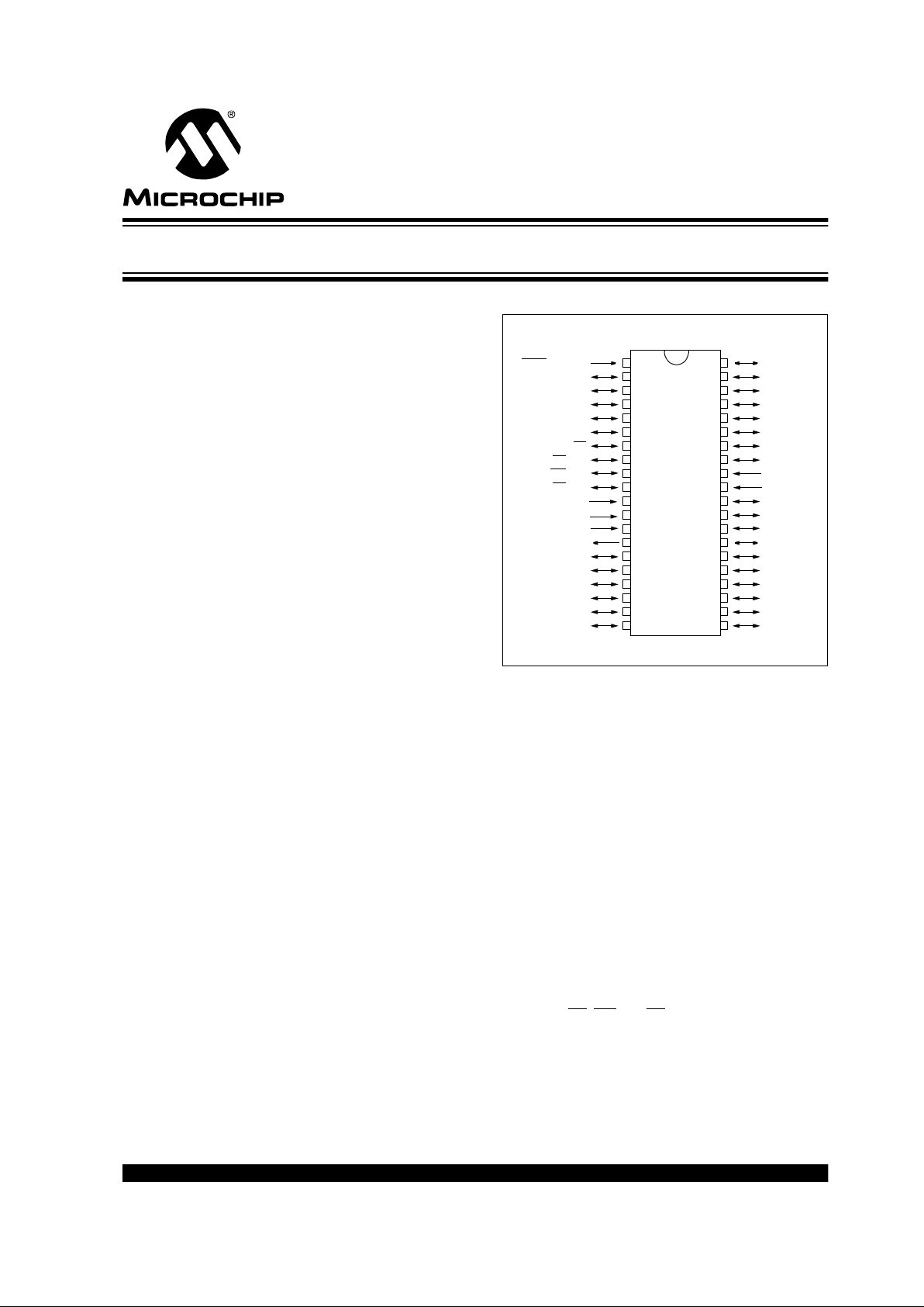
Pin Diagram
Peripheral Features:
• Timer0: 8-bit timer/counter with 8-bit prescaler
• Timer1: 16-bit timer/counter with prescaler,
can be incremented during sleep via external
crystal/clock
• Timer2: 8-bit timer/counter with 8-bit period
register, prescaler and postscaler
• Two Capture, Compare, PWM modules
- Capture is 16-bit, max. resolution is 12.5 ns
- Compare is 16-bit, max. resolution is 200 ns
- PWM max. resolution is 10-bit
• 10-bit multi-channel Analog-to-Digital converter
• Synchronous Serial Port (SSP) with SPI
(Master
Mode) and I
2C
(Master/Slave)
• Universal Synchronous Asynchronous Receiver
Transmitter (USART/SCI) with 9-bit address
detection
• Paralle l Slave P o rt (PSP) 8-bits wide, with
external RD
, WR and CS controls (40/44-pin only)
• Brown-out detection circuitry for
Brown-out Reset (BOR)
•PIC16F873
•PIC16F874
•PIC16F876
•PIC16F877
RB7/PGD
RB6/PGC
RB5
RB4
RB3/PGM
RB2
RB1
RB0/INT
VDD
VSS
RD7/PSP7
RD6/PSP6
RD5/PSP5
RD4/PSP4
RC7/RX/DT
RC6/TX/CK
RC5/SDO
RC4/SDI/SDA
RD3/PSP3
RD2/PSP2
MCLR/VPP/THV
RA0/AN0
RA1/AN1
RA2/AN2/VREF-
RA3/AN3/VREF+
RA4/T0CKI
RA5/AN4/SS
RE0/RD/AN5
RE1/WR/AN6
RE2/CS/AN7
VDD
VSS
OSC1/CLKIN
OSC2/CLKOUT
RC0/T1OSO/T1CKI
RC1/T1OSI/CCP2
RC2/CCP1
RC3/SCK/SCL
RD0/PSP0
RD1/PSP1
1
2
3
4
5
6
7
8
9
10
11
12
13
14
15
16
17
18
19
20
40
39
38
37
36
35
34
33
32
31
30
29
28
27
26
25
24
23
22
21
PIC16F877/874
PDIP
PIC16F87X
28/40-pin 8-Bit CMOS FLASH Microcontrollers
PIC16F87X
DS30292B-page 2
1999 Microchip Technology Inc.
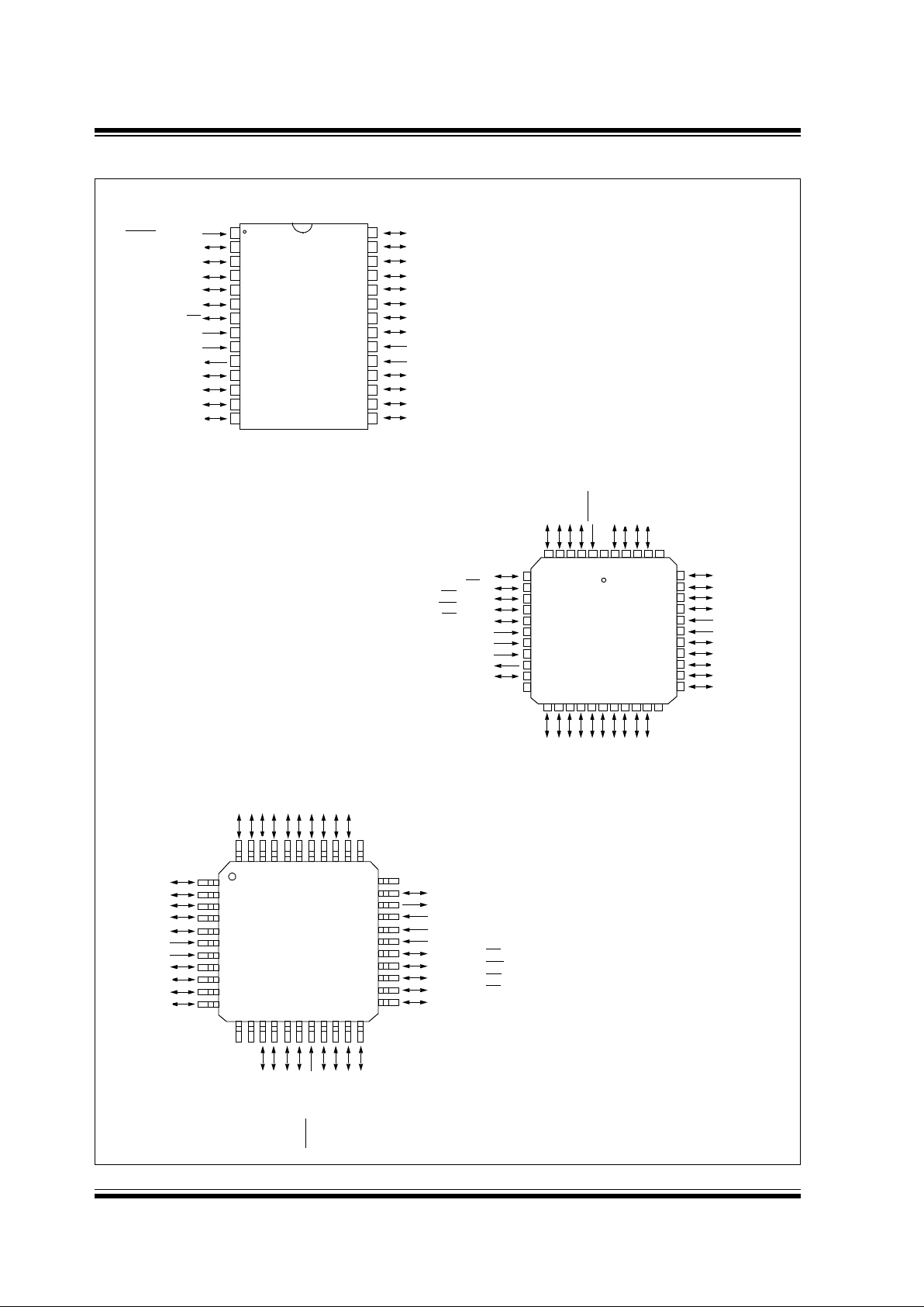
Pin Diagrams
PIC16F876/873
10
11
2
3
4
5
6
1
8
7
9
12
13
14
15
16
17
18
19
20
23
24
25
26
27
28
22
21
MCLR/VPP/THV
RA0/AN0
RA1/AN1
RA2/AN2/V
REF-
RA3/AN3/V
REF+
RA4/T0CKI
RA5/AN4/SS
VSS
OSC1/CLKIN
OSC2/CLKOUT
RC0/T1OSO/T1CKI
RC1/T1OSI/CCP2
RC2/CCP1
RC3/SCK/SCL
RB7/PGD
RB6/PGC
RB5
RB4
RB3/PGM
RB2
RB1
RB0/INT
V
DD
VSS
RC7/RX/DT
RC6/TX/CK
RC5/SDO
RC4/SDI/SDA
10
11
12
13
14
15
16
17
181920212223242526
44
8
7
65432
1
27
28
29
30
31
32
33
34
35
36
37
38
39
40
41
42
43
9
PIC16F877
RA4/T0CKI
RA5/AN4/SS
RE0/RD/AN5
OSC1/CLKIN
OSC2/CLKOUT
RC0/T1OSO/T1CK1
NC
RE1/WR
/AN6
RE2/CS
/AN7
V
DD
VSS
RB3/PGM
RB2
RB1
RB0/INT
V
DD
VSS
RD7/PSP7
RD6/PSP6
RD5/PSP5
RD4/PSP4
RC7/RX/DT
RA3/AN3/VREF+
RA2/AN2/V
REF-
RA1/AN1
RA0/AN0
MCLR
/VPP/THV
NC
RB7/PGD
RB6/PGC
RB5
RB4
NC
NC
RC6/TX/CK
RC5/SDO
RC4/SDI/SDA
RD3/PSP3
RD2/PSP2
RD1/PSP1
RD0/PSP0
RC3/SCK/SCL
RC2/CCP1
RC1/T1OSI/CCP2
10
11
2
3
4
5
6
1
1819202122
121314
15
38
8
7
4443424140
39
16
17
29
30
31
32
33
23
24
25
26
27
28
363435
9
PIC16F877
37
RA3/AN3/VREF+
RA2/AN2/V
REF-
RA1/AN1
RA0/AN0
MCLR
/VPP/THV
NC
RB7/PGD
RB6/PGC
RB5
RB4
NC
RC6/TX/CK
RC5/SDO
RC4/SDI/SDA
RD3/PSP3
RD2/PSP2
RD1/PSP1
RD0/PSP0
RC3/SCK/SCL
RC2/CCP1
RC1/T1OSI/CCP2
NC
NC
RC0/T1OSO/T1CKI
OSC2/CLKOUT
OSC1/CLKIN
V
SS
VDD
RE2/AN7/CS
RE1/AN6/WR
RE0/AN5/RD
RA5/AN4/SS
RA4/T0CKI
RC7/RX/DT
RD4/PSP4
RD5/PSP5
RD6/PSP6
RD7/PSP7
V
SS
VDD
RB0/INT
RB1
RB2
RB3/PGM
PLCC
QFP
DIP, SOIC
PIC16F874
PIC16F874
1999 Microchip Technology Inc. DS30292B-page 3
PIC16F87X
Key Features
PICmicro™ Mid-Range Reference
Manual (DS33023)
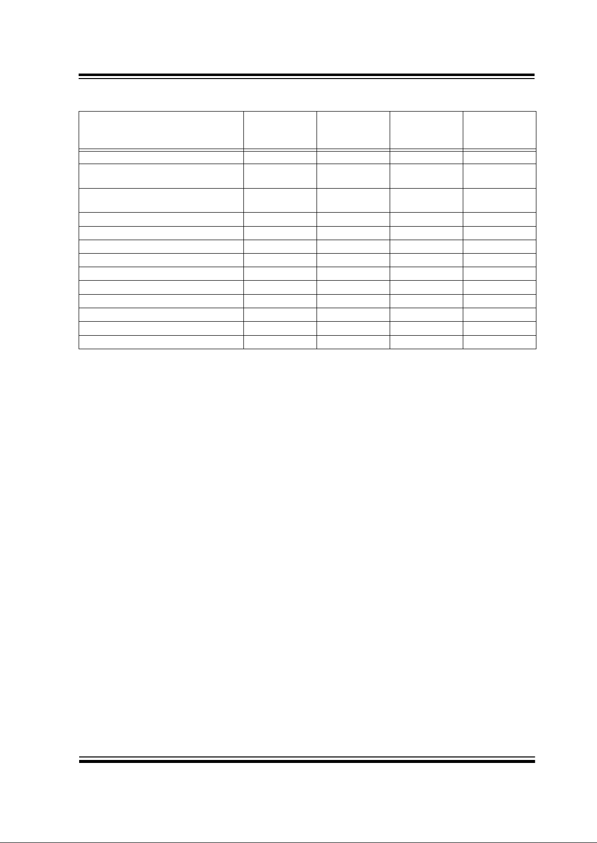
PIC16F873 PIC16F874 PIC16F876 PIC16F877
Operating Frequency DC - 20 MHz DC - 20 MHz DC - 20 MHz DC - 20 MHz
Resets (and Delays) POR, BOR
(PWRT, OST)
POR, BOR
(PWRT, OST)
POR, BOR
(PWRT, OST)
POR, BOR
(PWRT, OST)
FLASH Program Memory
(14-bit words)
4K 4K 8K 8K
Data Memory (bytes) 192 192 368 368
EEPROM Data Memory 128 128 256 256
Interrupts 13 14 13 14
I/O Ports Ports A,B,C Ports A,B,C,D,E Ports A,B,C Ports A,B,C,D,E
Timers 3333
Capture/Compare/PWM modules 2 2 2 2
Serial Communications MSSP, USART MSSP, USART MSSP, USART MSSP, USART
Parallel Communications — PSP — PSP
10-bit Analog-to-Digital Module 5 input channels 8 input channels 5 input channels 8 input channels
Instruction Set 35 Instructions 35 Instructions 35 Instructions 35 Instructions

PIC16F87X
DS30292B-page 4
1999 Microchip Technology Inc.
Table of Contents
1.0 Device Overview...........................................................................................................................................................................5
2.0 Memory Organization..................................................................................................................................................................11
3.0 I/O Ports.................... .......................... ......................... ...................................... ........................... ..............................................29
4.0 Data EEPROM and FLASH Program Memory ...........................................................................................................................41
5.0 Timer0 Module............................................................................................................................................................................47
6.0 Timer1 Module............................................................................................................................................................................51
7.0 Timer2 Module........................................................................................................................................................................... 55
8.0 Capture/Compare/PWM (CCP) Module(s)..................................................................................................................................57
9.0 Master Synchronous Serial Port (MSSP) Module.......................................................................................................................63
10.0 Universal Synchronous Asynchronous Receiver Transmitter (USART) .....................................................................................95
11.0 Analog-to-Digital Converter (A/D) Module................................................................................................................................. 111
12.0 Special Features of the CPU.....................................................................................................................................................121
13.0 Instruction Set Summary...........................................................................................................................................................137
14.0 Development Support ...............................................................................................................................................................145
15.0 Electrical Characteristics........................................................................................................................................................... 151
16.0 DC and AC Characteristics Graphs and Tables........................................................................................................................173
17.0 Packaging Infor mation............. ............................................................... ..................................................................................175
Appendix A: Revision History.........................................................................................................................................................183
Appendix B: Device Differences.....................................................................................................................................................183
Appendix C: Conversion Considerations............................................................ ....... .. .... .. .... .. ....... .. ..............................................183
Index ...................................... .. ....... .. .. .. .. .. .. .. ..... .. .. .. .... .. .. .. ..... .. .. .. .. .. .. .. .. ....... .. .. .. .. .. ...........................................................185
On-Line Support.................................................................... .... .... .. ......... .... .. .... .... ....... .... ................................................................. 191
Product Identification System............................................................................................................................................................. 193
To Our Valued Customers
Most Current Data Sheet
To obtain the most up-to-date version of this data sheet, please register at our Worldwide Web site at:
http://www.microchip.com
You can determine the version of a data sheet by examining its literature number found on the bottom outside corner of any page.
The last character of the literature number is the version number. e.g., DS30000A is version A of document DS30000.
New Customer Notification System
Register on our web site (www.microchip.com/cn) to receive the most current information on our products.
Errata
An errata sheet may exist for current devices, describing minor operational differences (from the data sheet) and recommended
workarounds. As device/documentation issues become known to us, we wil l pub lish an errata sheet. The errata will specify the revision of silicon and revision of document to which it applies.
To determine if an errata sheet exists for a particular device, please check with one of the following:
• Microchip’s Worldwide Web site; http://www.microchip.com
• Your local Microchip sales office (see last page)
• The Microchip Corporate Literature Center; U.S. FAX: (480) 786-7277
When contacting a sales office or the literature center, please specify which device, revision of silicon and data sheet (include liter-
ature number) you are using.
Corrections to this Data Sheet
We constantly strive to improve the quality of all our products and documentation. We have spent a great deal of time to ensure
that this document is correct. However , w e realize that we ma y have missed a few things. If you fi nd any inf ormation that is missin g
or appears in error, please:
• Fill out and mail in the reader response form in the back of this data sheet.
• E-mail us at webmaster@microchip.com.
We appreciate your assistance in making this a better document.
1999 Microchip Technology Inc. DS30292B-page 5
PIC16F87X
1.0 DEVICE OVERVIEW
This document contains device-specific information.
Additional information may be found in the PICmicro™
Mid-Range Reference Manual, (DS33023), which may
be obtained from your local Microchip Sales Representative or downloaded from the Microchip website. The
Reference Manual should be considered a complementary document to this data she et, and is high ly recommended reading for a better understanding of the
device architecture and operation of the peripheral
modules.
There are four devices (PIC16F873, PIC16F874,
PIC16F876 and PIC16F877) covered by this data
sheet. The PIC16F876/873 devices come in 28-pin
packages and th e PIC16F87 7/874 de vic es come in 40pin packages. The 28-pin devices do not have a Parallel Slave Port implemented.
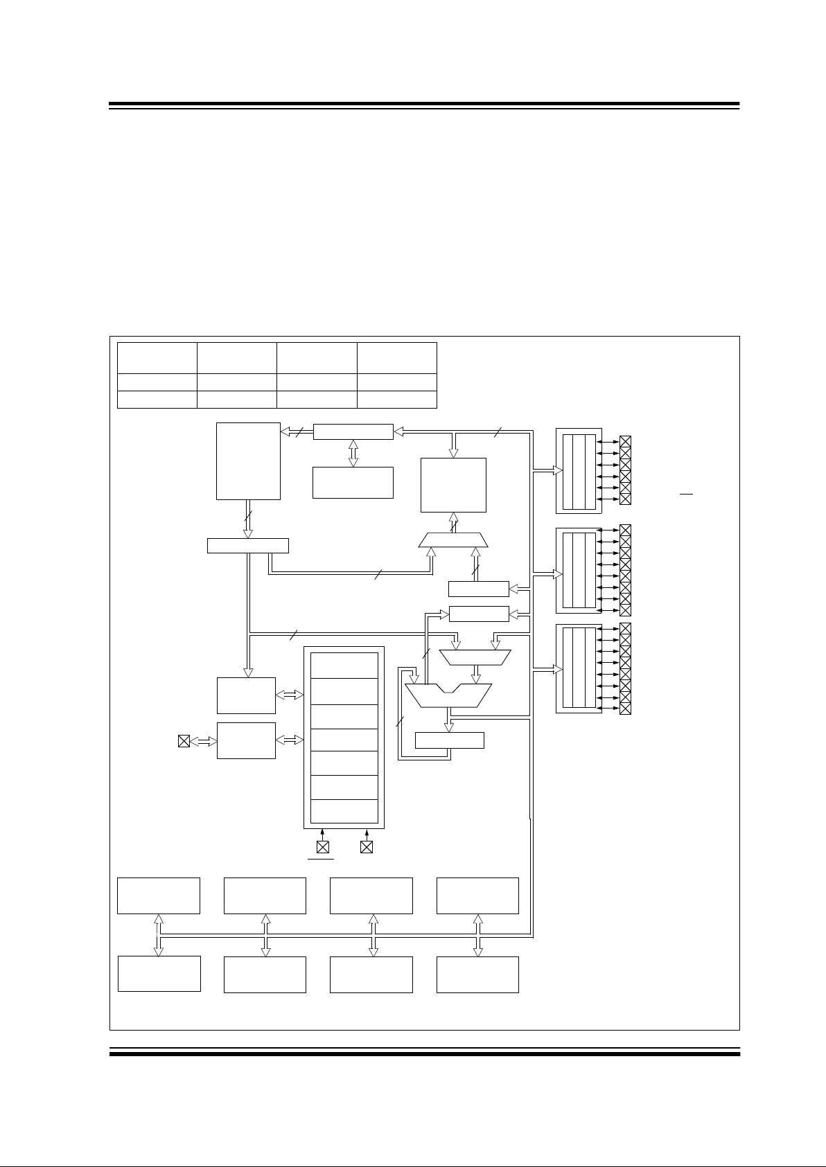
The following two figures are device block diagrams
sorted by pin number; 28-pin for Figure 1-1 and 40-pin
for Figure 1-2. The 28-pin and 40-pin pinouts are listed
in Table 1-1 and Table 1-2, respectively.
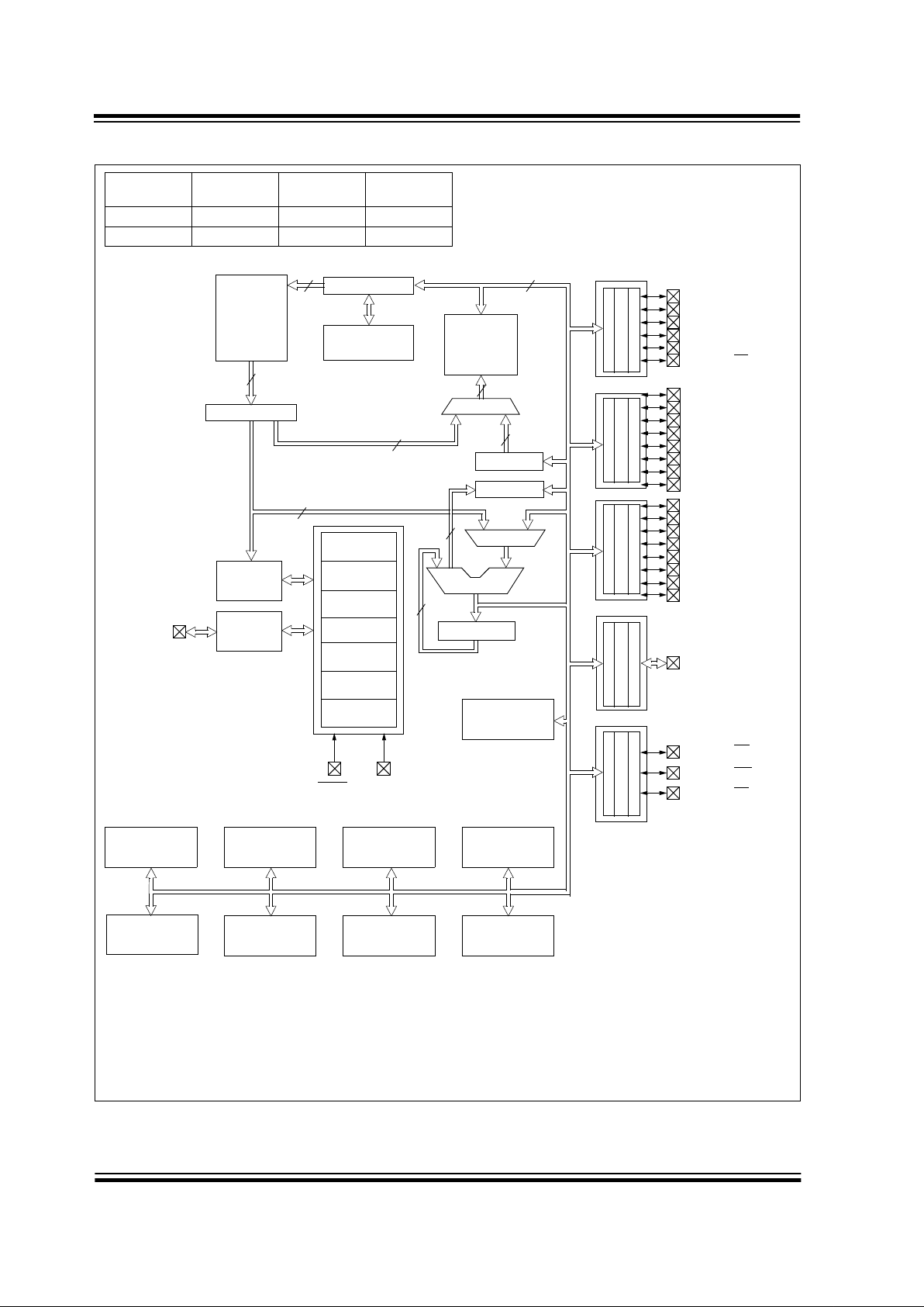
FIGURE 1-1: PIC16F873 AND PIC16F876 BLOCK DIAGRAM
FLASH
Program
Memory
13
Data Bus
8
14
Program
Bus
Instruction reg
Program Counter
8 Level Stack
(13-bit)
RAM
File
Registers
Direct Addr
7
RAM Addr (1)
9
Addr MUX
Indirect
Addr
FSR reg
STATUS reg
MUX
ALU
W reg
Power-up
Timer
Oscillator
Start-up Timer
Power-on
Reset
Watchdog
Timer
Instruction
Decode &
Control
Timing
Generation
OSC1/CLKIN
OSC2/CLKOUT
MCLR
VDD, VSS
PORTA
PORTB
PORTC
RA4/T0CKI
RA5/AN4/SS
RB0/INT
RC0/T1OSO/T1CKI
RC1/T1OSI/CCP2
RC2/CCP1
RC3/SCK/SCL
RC4/SDI/SDA
RC5/SDO
RC6/TX/CK
RC7/RX/DT
8
8
Brown-out
Reset
Note 1: Higher order bits are from the STATUS register.
USART
CCP1,2
Synchronous
10-bit A/DTimer0 Timer1 Timer2
Serial Port
RA3/AN3/VREF+
RA2/AN2/VREF-
RA1/AN1
RA0/AN0
8
3
Data EEPROM
RB1
RB2
RB3/PGM
RB4
RB5
RB6/PGC
RB7/PGD
Device Program
FLASH
Data Memory Data
EEPROM
PIC16F873 4K 192 Bytes 128 Bytes
PIC16F876 8K 368 Bytes 256 Bytes
In-Circuit
Debugger
Low-Voltage
Programming
PIC16F87X
DS30292B-page 6
1999 Microchip Technology Inc.
FIGURE 1-2: PIC16F874 AND PIC16F877 BLOCK DIAGRAM
FLASH
Program
Memory
13
Data Bus
8
14
Program
Bus
Instruction reg
Program Counter
8 Level Stack
(13-bit)
RAM
File
Registers
Direct Addr
7
RAM Addr (1)
9
Addr MUX
Indirect
Addr
FSR reg
STATUS reg
MUX
ALU
W reg
Power-up
Timer
Oscillator
Start-up Tim er
Power-on
Reset
Watchdog
Timer
Instruction
Decode &
Control
Timing
Generation
OSC1/CLKIN
OSC2/CLKOUT
MCLR
VDD, VSS
PORTA
PORTB
PORTC
PORTD
PORTE
RA4/T0CKI
RA5/AN4/SS
RC0/T1OSO/T1CKI
RC1/T1OSI/CCP2
RC2/CCP1
RC3/SCK/SCL
RC4/SDI/SDA
RC5/SDO
RC6/TX/CK
RC7/RX/DT
RD7/PSP7:RD0/PSP0
RE0/AN5/RD
RE1/AN6/WR
RE2/AN7/CS
8
8
Brown-out
Reset
Note 1: Higher order bits are from the STATUS register.
USART
CCP1,2
Synchronous
10-bit A/DTimer0 Timer1 Timer2
Serial Port
RA3/AN3/VREF+
RA2/AN2/VREF-
RA1/AN1
RA0/AN0
Parallel Slave Port
8
3
Data EEPROM
RB0/INT
RB1
RB2
RB3/PGM
RB4
RB5
RB6/PGC
RB7/PGD
Device Program
FLASH
Data Memory Data
EEPROM
PIC16F874 4K 192 Bytes 128 Bytes
PIC16F877 8K 368 Bytes 256 Bytes
In-Circuit
Debugger
Low-Voltage
Programming

1999 Microchip Technology Inc. DS30292B-page 7
PIC16F87X
TABLE 1-1: PIC16F873 AND PIC16F876 PINOUT DESCRIPTION
Pin Name
DIP
Pin#
SOIC
Pin#
I/O/P
Type
Buffer
Type
Description
OSC1/CLKIN 9 9 I
ST/CMOS
(3)
Oscillator crystal input/external clock source input.
OSC2/CLKOUT 10 10 O — Oscillator crystal output. Connects to crystal or resonator in crystal
oscillator mode. In RC mode, the OSC2 pin outputs CLKOUT
which has 1/4 the frequency of OSC1 , and denot es th e instruc tion
cycle rate.
MCLR
/VPP/THV 1 1 I/P ST Master clear (reset) input or programming vo ltage input or high
voltage test mode control. This pin is an active low reset to the
device.
PORTA is a bi-directional I/O port.
RA0/AN0 2 2 I/O TTL RA0 can also be analog input0
RA1/AN1 3 3 I/O TTL RA1 can also be analog input1
RA2/AN2/V
REF- 4 4 I/O TTL RA2 can also be analog input2 or negative analog reference
voltage
RA3/AN3/V
REF+ 5 5 I/O TTL RA3 can also be analog input3 or positive analog reference
voltage
RA4/T0CKI 6 6 I/O ST RA4 can also be the clock input to the Timer0 module. Output
is open drain type.
RA5/SS/
AN4 7 7 I/O TTL RA5 can also be analog input4 or the slave select for the
synchronous serial port.
PORTB is a bi-directi onal I/O port. PORTB can be software
programmed for internal weak pull-up on all inputs.
RB0/INT 21 21 I/O
TTL/ST
(1)
RB0 can also be the exte rnal interrupt pin.
RB1 22 22 I/O TTL
RB2 23 23 I/O TTL
RB3/PGM 24 24 I/ O TTL R B3 can also be t he low volt a g e programming in put
RB4 25 25 I/ O TT L Interrupt on chan g e pi n .
RB5 26 26 I/ O TT L Interrupt on chan g e pi n .
RB6/PGC 27 27 I/O
TTL/ST
(2)
Interrupt on change pin or In-Circuit Debugger pin. Serial
programming clock.
RB7/PGD 28 28 I/O
TTL/ST
(2)
Interrupt on change pin or In-Circuit Debugger pin. Serial
programming data.
PORTC is a bi-directional I/O port.
RC0/T1OSO /T 1 C K I 11 11 I/O ST RC0 can al s o be th e T i m e r1 oscillator ou tp u t or T i m er 1 cl ock
input.
RC1/T1OSI/CCP2 12 12 I/O ST RC1 can also be the Timer 1 oscillator input or Capt ure2 input/
Compare2 output/PWM2 output.
RC2/CCP1 13 13 I/O ST RC2 can also be the Capt ure1 input/ Compare1 output/ PWM1
output.
RC3/SCK/SCL 14 14 I/O ST RC3 can also be t he s ynchro nous s erial cl ock input/output for
both SPI and I
2
C modes.
RC4/SDI/SDA 15 15 I/O ST RC4 can also be the SPI Data In (SPI mode) or
data I/O (I
2
C mode).
RC5/SDO 16 16 I/O ST RC5 can also be the SPI Data Out (SPI mode).
RC6/TX/CK 17 17 I/O ST RC6 can also be the USART Asynchronous Transmit or
Synchron ou s C l ock.
RC7/RX/DT 18 18 I/O ST RC7 can also be the USART Asynchronous Receive or
Synchron ou s D at a.
V
SS 8, 19 8, 19 P — Ground reference for logic and I/ O pins.
V
DD 20 20 P — Positive supply for logic and I/O pins.
Legend: I = input O = output I/O = input/output P = power
— = Not used TTL = TTL input ST = Schmitt Trigger input
Note 1: This buffer is a Sc hmitt Trigger input when config ured as the external interrupt.
2: This buffer is a Schmitt Trigger input when used in serial programming mode.
3: This buffer is a Schmitt Trigger input when configured in RC oscillator mode and a CMOS input otherwise.

PIC16F87X
DS30292B-page 8
1999 Microchip Technology Inc.
TABLE 1-2: PIC16F874 AND PIC16F877 PINOUT DESCRIPTION
Pin Name
DIP
Pin#
PLCC
Pin#
QFP
Pin#
I/O/P
Type
Buffer
Type
Description
OSC1/CLKIN 13 14 30 I
ST/CMOS
(4)
Oscillator crystal input/external clock source input.
OSC2/CLKOUT 14 15 31 O — Oscillator crystal output. Connects to crystal or resonator in
crystal oscillator mode. In RC mode, OSC2 pin outputs CLKOUT which has 1/4 the frequency of OSC1, and denotes the
instruction cycle rate.
MCLR
/VPP/THV 1 2 18 I/P ST Master clear (reset) input or pr og ramming v olt ag e input o r hig h
voltage test mode control. This pin is an active low reset to the
device.
PORTA is a bi-directional I/O port.
RA0/AN0 2 3 19 I/O TTL RA0 can also be analog input0
RA1/AN1 3 4 20 I/O TTL RA1 can also be analog input1
RA2/AN2/V
REF- 4 5 21 I/O TTL RA2 can also be analog input2 or negative analog
reference voltage
RA3/AN3/V
REF+ 5 6 22 I/O TTL RA3 can also be analog input3 or positive analog
reference voltage
RA4/T0CKI 6 7 23 I/O ST RA4 can also be the clock input to the Timer0 timer/
counter. Output is open drain type.
RA5/SS/
AN4 7 8 24 I/O TTL RA5 can also be analog input4 or the slave select for the
synchronous serial port.
PORTB is a bi-directional I/O port. PORTB can be software
programmed for internal weak pull-up on all inputs.
RB0/INT 33 36 8 I/O
TTL/ST
(1)
RB0 can also be the exte rnal interrupt pin.
RB1 34 37 9 I/O TTL
RB2 35 38 10 I/O TTL
RB3/PGM 36 39 11 I/O TTL RB3 can also be the low v oltage programming inp ut
RB4 37 41 14 I/O TTL Interrupt on change pin.
RB5 38 42 15 I/O TTL Interrupt on change pin.
RB6/PGC 39 43 16 I/O
TTL/ST
(2)
Interrupt on change pin or In-Circuit Debugger pin. Serial
programming clock.
RB7/PGD 40 44 17 I/O
TTL/ST
(2)
Interrupt on change pin or In-Circuit Debugger pin. Serial
programming data.
PORTC is a bi-directional I/O port.
RC0/T1OSO/T1CKI 15 16 32 I/O ST RC0 can also be the Timer1 oscillator output or a Timer1
clock input.
RC1/T1OSI/CCP2 16 18 35 I/O ST RC1 can also be the Timer1 oscillator input or Capture2
input/Compare2 output/PWM2 output.
RC2/CCP1 17 19 36 I/O ST RC2 can also be the Capture1 input/Compare1 output/
PWM1 output.
RC3/SCK/SCL 18 20 37 I/O ST RC3 can also be the synchro nous seria l cloc k in put/out put
for both SPI and I
2
C modes.
RC4/SDI/SDA 23 25 42 I/O ST RC4 can also be the SPI Data In (SPI mode) or
data I/O (I
2
C mode).
RC5/SDO 24 26 43 I/O ST RC5 can also be th e SP I D at a Ou t
(SPI mode).
RC6/TX/CK 25 27 44 I/O ST RC6 can also be the USART Asynchronous Transmit or
Synchronous Clock.
RC7/RX/DT 26 29 1 I/O ST RC7 can also be the USART Asynchronous Receive or
Synchronous Data.
Legend: I = input O = output I/O = input/output P = power
— = Not used TTL = TTL input ST = Schmitt Trigger input
Note 1: This buffer is a Sc hmitt Trigger input when config ured as an external interrupt.
2: This buffer is a Schmitt Trigger input when used in serial programming mode.
3: This buffer is a Schmitt Trigger input when configured as general pu rpose I/O and a TTL input when used in the Parallel Slave
Port mode (for int erfacing to a microprocess o r bus ) .
4: This buffer is a Schmitt Trigger input when configured in RC oscillator mode and a CMOS input otherwise.
1999 Microchip Technology Inc. DS30292B-page 9
PIC16F87X
PORTD is a bi-directional I/O port or parallel slave port when
interfacing to a mi croprocessor bus.
RD0/PSP0 19 21 38 I/O
ST/TTL
(3)
RD1/PSP1 20 22 39 I/O
ST/TTL
(3)
RD2/PSP2 21 23 40 I/O
ST/TTL
(3)
RD3/PSP3 22 24 41 I/O
ST/TTL
(3)
RD4/PSP4 27 30 2 I/O
ST/TTL
(3)
RD5/PSP5 28 31 3 I/O
ST/TTL
(3)
RD6/PSP6 29 32 4 I/O
ST/TTL
(3)
RD7/PSP7 30 33 5 I/O
ST/TTL
(3)
PORTE is a bi-directional I/O port.
RE0/RD
/AN5 8 9 25 I/O
ST/TTL
(3)
RE0 can also be read control fo r the par alle l sla v e port, or
analog input5.
RE1/WR
/AN6 9 10 26 I/O
ST/TTL
(3)
RE1 can also be write control for the parallel slave port, or
analog input6.
RE2/CS
/AN7 10 11 27 I/O
ST/TTL
(3)
RE2 can also be select control for the parallel slave port,
or analog input7.
V
SS 12,31 13,34 6,29 P — Ground reference for logic and I/O pins.
V
DD 11,32 12,35 7,28 P — Positive supply for logic and I/O pins.
NC — 1,17,28,4012,13,
33,34
— These pins are not internally connect ed. These pins should be
left unconnected.
TABLE 1-2: PIC16F874 AND PIC16F877 PINOUT DESCRIPTION (CONTINUED)
Pin Name
DIP
Pin#
PLCC
Pin#
QFP
Pin#
I/O/P
Type
Buffer
Type
Description
Legend: I = input O = output I/O = input/output P = power
— = Not used TTL = TTL input ST = Schmitt Trigger input
Note 1: This buffer is a Sc hmitt Trigger input when config ured as an external interrupt.
2: This buffer is a Schmitt Trigger input when used in serial programming mode.
3: This buffer is a Schmitt Trigger input when configured as general pu rpose I/O and a TT L input when used in the Parallel Slave
Port mode (for int erfacing to a microprocess o r bus ) .
4: This buffer is a Schmitt Trigger input when configured in RC oscillator mode and a CMOS input otherwise.

PIC16F87X
DS30292B-page 10
1999 Microchip Technology Inc.
NOTES:
1999 Microchip Technology Inc. DS30292B-page 11
PIC16F87X
2.0 MEMORY ORGANIZATION
There are three memory blocks in each of these
PICmicro MCUs. The Program Memory and Data
Memory have separate buses so that concurrent
access can occur and is detailed in this section. The
EEPROM data memory block is detailed in
Section 4.0.
Additional inf ormation on de vice m emory may be f ound
in the PICmicro Mid-Range Reference Manual,
(DS33023).
2.1 Program Memory Organization
The PIC16F87X de vices ha ve a 13-bit prog ram coun ter
capable of addressing an 8K x 14 program memory
space. The PIC16F877/876 devices have 8K x 14
words of FLASH progr am memory and the PIC16F873/
874 devices have 4K x 14. Accessing a location above
the physically implemented address will cause a wraparound.
The reset vector is at 0000h and the interrupt vector is
at 0004h.
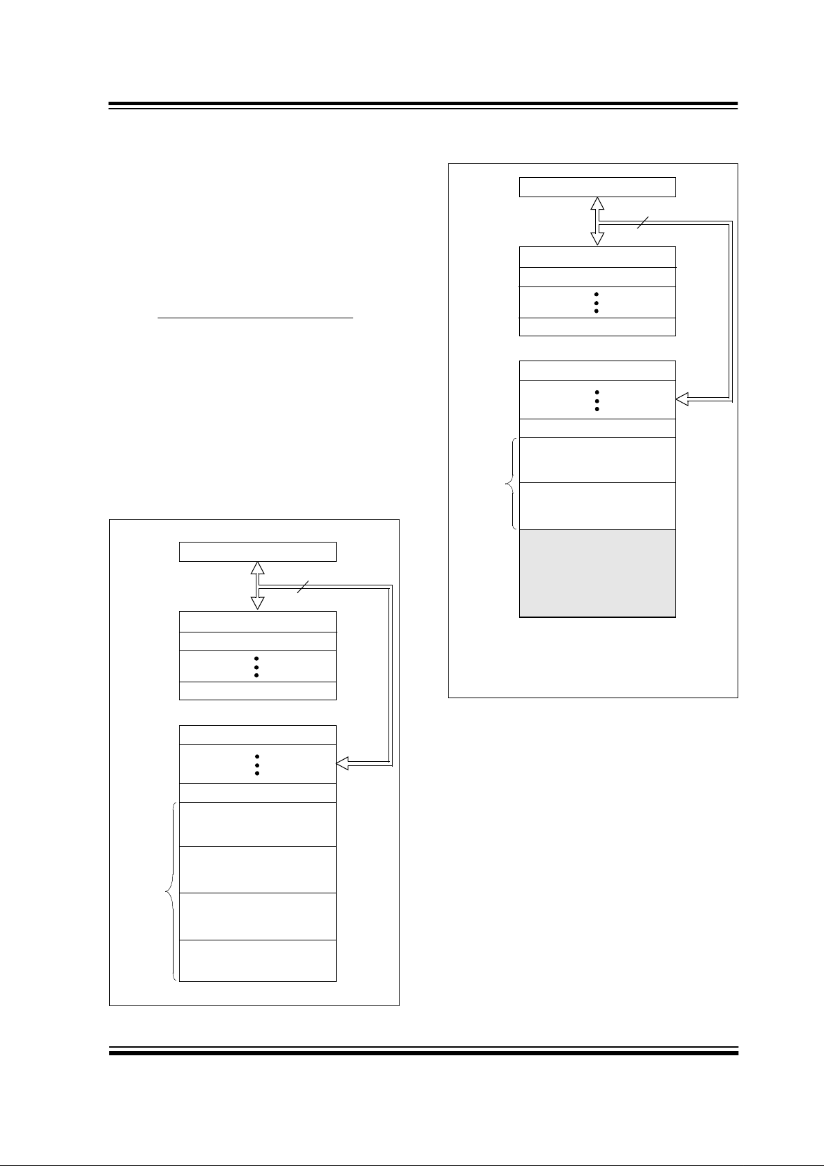
FIGURE 2-1: PIC16F877/876 PROGRAM
MEMORY MAP AND STACK
FIGURE 2-2: PIC16F874/873 PROGRAM
MEMORY MAP AND STACK
PC<12:0>
13
0000h
0004h
0005h
Stack Level 1
Stack Level 8
Reset Vector
Interrupt Vector
On-Chip
CALL, RETURN
RETFIE, RETLW
1FFFh
Stack Level 2
Program
Memory
Page 0
Page 1
Page 2
Page 3
07FFh
0800h
0FFFh
1000h
17FFh
1800h
PC<12:0>
13
0000h
0004h
0005h
Stack Level 1
Stack Level 8
Reset Vector
Interrupt Vector
On-Chip
CALL, RETURN
RETFIE, RETLW
1FFFh
Stack Level 2
Program
Memory
Page 0
Page 1
07FFh
0800h
0FFFh
1000h

PIC16F87X
DS30292B-page 12
1999 Microchip Technology Inc.
2.2 Data Memory Organization
The data memory is partitioned into multiple banks
which contain the General Purpose Registers and the
Special Function Regi sters. Bits RP1( STA TUS<6>) and
RP0 (STATUS<5>) are the bank select bits.
Each bank extends up to 7Fh (128 bytes). The lower
locations of each bank are reserved for the Special
Function Registers . Abo v e the Sp ecial Functi on Regi sters are General Purpose Registers, implemented as
static RAM. All implemented banks contain Special
Function Registers. Some “high use” Special Function
Registers from one bank may be mirrored in another
bank for code reduction and quicker access.
2.2.1 GENERAL PURPOSE REGISTER FILE
The register file can be accessed either directly, or indi-
rectly through the File Select Register FSR.
RP1:RP0 Bank
00 0
01 1
10 2
11 3
Note: EEPROM Data Memory description can b e
found in Section 4.0 of this Data Sheet
1999 Microchip Technology Inc. DS30292B-page 13
PIC16F87X
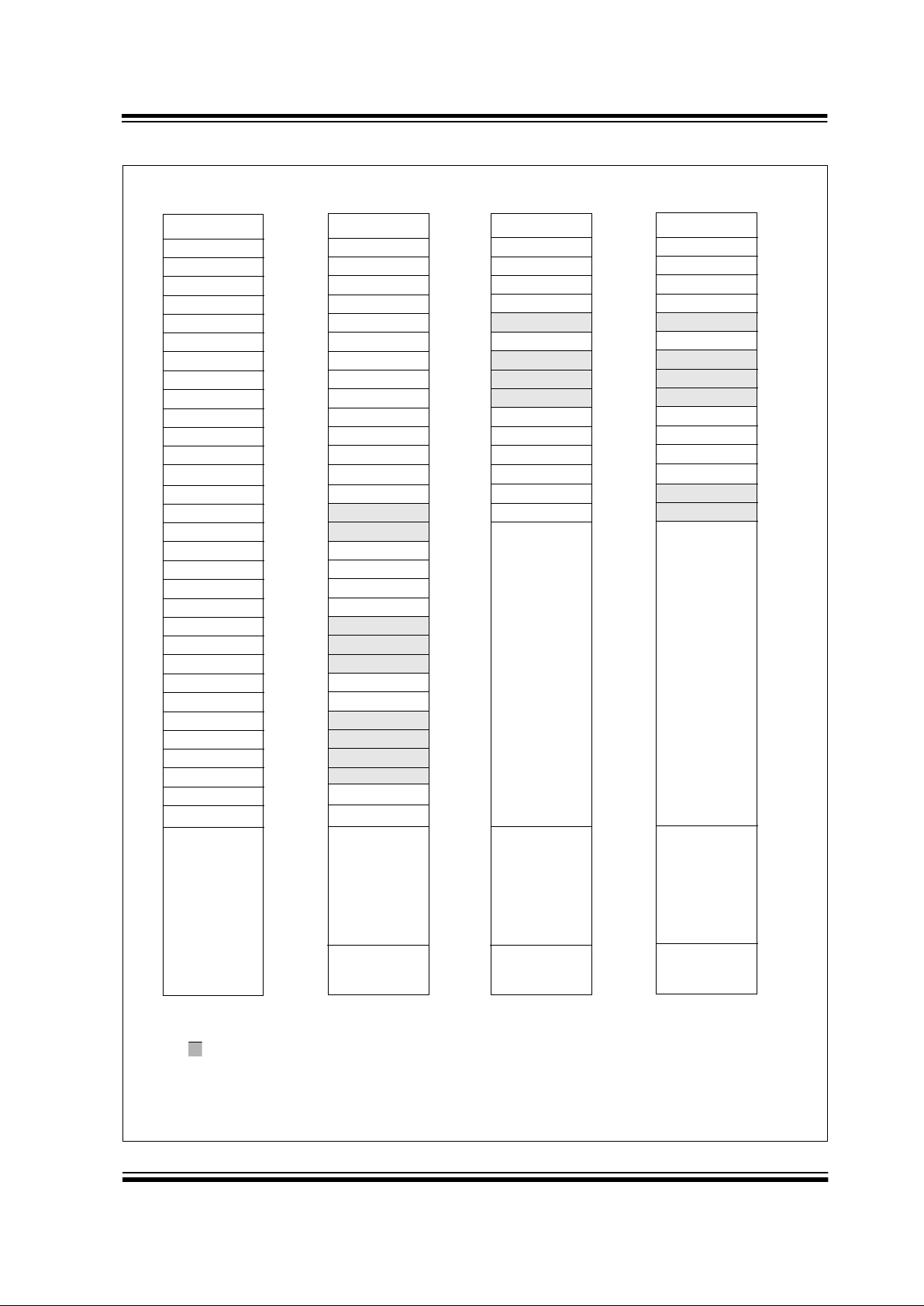
FIGURE 2-3: PIC16F877/876 REGISTER FILE MAP
Indirect addr.
(*)
TMR0
PCL
STATUS
FSR
PORTA
PORTB
PORTC
PCLATH
INTCON
PIR1
TMR1L
TMR1H
T1CON
TMR2
T2CON
SSPBUF
SSPCON
CCPR1L
CCPR1H
CCP1CON
OPTION_REG
PCL
STATUS
FSR
TRISA
TRISB
TRISC
PCLATH
INTCON
PIE1
PCON
PR2
SSPADD
SSPSTAT
00h
01h
02h
03h
04h
05h
06h
07h
08h
09h
0Ah
0Bh
0Ch
0Dh
0Eh
0Fh
10h
11h
12h
13h
14h
15h
16h
17h
18h
19h
1Ah
1Bh
1Ch
1Dh
1Eh
1Fh
80h
81h
82h
83h
84h
85h
86h
87h
88h
89h
8Ah
8Bh
8Ch
8Dh
8Eh
8Fh
90h
91h
92h
93h
94h
95h
96h
97h
98h
99h
9Ah
9Bh
9Ch
9Dh
9Eh
9Fh
20h
A0h
7Fh
FFh
Bank 0
Bank 1
Unimplemented data memory locations, read as ’0’.
* Not a physical register.
Note 1: These registers are not implemented on 28-pin devices.
2: These registers are reserved, maintain these registers clear.
File
Address
Indirect addr.
(*)
Indirect addr.
(*)
PCL
STATUS
FSR
PCLATH
INTCON
PCL
STATUS
FSR
PCLATH
INTCON
100h
101h
102h
103h
104h
105h
106h
107h
108h
109h
10Ah
10Bh
10Ch
10Dh
10Eh
10Fh
110h
111h
112h
113h
114h
115h
116h
117h
118h
119h
11Ah
11Bh
11Ch
11Dh
11Eh
11Fh
180h
181h
182h
183h
184h
185h
186h
187h
188h
189h
18Ah
18Bh
18Ch
18Dh
18Eh
18Fh
190h
191h
192h
193h
194h
195h
196h
197h
198h
199h
19Ah
19Bh
19Ch
19Dh
19Eh
19Fh
120h
1A0h
17Fh
1FFh
Bank 2
Bank 3
Indirect addr.
(*)
PORTD
PORTE
TRISD
ADRESL
TRISE
TMR0
OPTION_REG
PIR2
PIE2
RCSTA
TXREG
RCREG
CCPR2L
CCPR2H
CCP2CON
ADRESH
ADCON0
TXSTA
SPBRG
ADCON1
General
Purpose
Register
General
Purpose
Register
General
Purpose
Register
General
Purpose
Register
1EFh
1F0h
accesses
70h - 7Fh
EFh
F0h
accesses
70h-7Fh
16Fh
170h
accesses
70h-7Fh
General
Purpose
Register
General
Purpose
Register
TRISB
PORTB
96 Bytes
80 Bytes 80 Bytes 80 Bytes
16 Bytes
16 Bytes
(1)
(1)
(1)
(1)
SSPCON2
EEDATA
EEADR
EECON1
EECON2
EEDATH
EEADRH
Reserved
(2)
Reserved
(2)
PIC16F87X
DS30292B-page 14
1999 Microchip Technology Inc.
FIGURE 2-4: PIC16F874/873 REGISTER FILE MAP
Indirect addr.
(*)
TMR0
PCL
STATUS
FSR
PORTA
PORTB
PORTC
PCLATH
INTCON
PIR1
TMR1L
TMR1H
T1CON
TMR2
T2CON
SSPBUF
SSPCON
CCPR1L
CCPR1H
CCP1CON
OPTION_REG
PCL
STATUS
FSR
TRISA
TRISB
TRISC
PCLATH
INTCON
PIE1
PCON
PR2
SSPADD
SSPSTAT
00h
01h
02h
03h
04h
05h
06h
07h
08h
09h
0Ah
0Bh
0Ch
0Dh
0Eh
0Fh
10h
11h
12h
13h
14h
15h
16h
17h
18h
19h
1Ah
1Bh
1Ch
1Dh
1Eh
1Fh
80h
81h
82h
83h
84h
85h
86h
87h
88h
89h
8Ah
8Bh
8Ch
8Dh
8Eh
8Fh
90h
91h
92h
93h
94h
95h
96h
97h
98h
99h
9Ah
9Bh
9Ch
9Dh
9Eh
9Fh
20h
A0h
7Fh
FFh
Bank 0
Bank 1
File
Address
Indirect addr .
(*)
Indirect addr.
(*)
PCL
STATUS
FSR
PCLATH
INTCON
PCL
STATUS
FSR
PCLATH
INTCON
100h
101h
102h
103h
104h
105h
106h
107h
108h
109h
10Ah
10Bh
180h
181h
182h
183h
184h
185h
186h
187h
188h
189h
18Ah
18Bh
17Fh
1FFh
Bank 2
Bank 3
Indirect addr.
(*)
PORTD
PORTE
TRISD
ADRESL
TRISE
TMR0
OPTION_REG
PIR2
PIE2
RCSTA
TXREG
RCREG
CCPR2L
CCPR2H
CCP2CON
ADRESH
ADCON0
TXSTA
SPBRG
ADCON1
General
Purpose
Register
General
Purpose
Register
1EFh
1F0h
accesses
A0h - FFh
16Fh
170h
accesses
20h-7Fh
TRISB
PORTB
96 Bytes
96 Bytes
(1)
(1)
(1)
(1)
SSPCON2
10Ch
10Dh
10Eh
10Fh
110h
18Ch
18Dh
18Eh
18Fh
190h
EEDATA
EEADR
EECON1
EECON2
EEDATH
EEADRH
Reserved
(2)
Reserved
(2)
Unimplemented data memory locations, read as ’0’.
* Not a physical register.
Note 1: These registers are not implemented on 28-pin devices.
2: These registers are reserved, maintain these registers clear.
120h
1A0h
1999 Microchip Technology Inc. DS30292B-page 15
PIC16F87X
2.2.2 SPECIAL FUNCTION REGISTERS
The Special Function Registers are registers used by
the CPU and peripheral modules for controlling the
desired operation of the device. These registers are
implemented as static RAM. A list of these registers is
given in Table 2-1.
The Special Function Registers can be classified into
two sets; core (CPU) and peripheral. Those registers
associated with the core functions are described in
detail in this section. Those related to the operation of
the peripheral features are described in detail in the
peripheral feature section.
TABLE 2-1: SPECIAL FUNCTION REGISTER SUMMARY
Addres
s
Name Bit 7 Bit 6 Bit 5 Bit 4 Bit 3 Bit 2 Bit 1 Bit 0
Val ue on :
POR,
BOR
Value on
all other
resets
(2)
Bank 0
00h
(4)
INDF Addressing this location uses contents of FSR to address data memory (not a physical register) 0000 0000 0000 0000
01h TMR0 Timer0 module’s register xxxx xxxx uuuu uuuu
02h
(4)
PCL Program Counter's (PC) Least Significant Byte 0000 0000 0000 0000
03h
(4)
STAT US IRP RP1 RP0 TO PD ZDCC0001 1xxx 000q quuu
04h
(4)
FSR Indirect data memory address pointer xxxx xxxx uuuu uuuu
05h PORTA
— — PORTA Data Latch when written: PORT A pins when read --0x 0000 --0u 0000
06h PORTB PORTB Data Latch when written: PORTB pins when read xxxx xxxx uuuu uuuu
07h PORTC PORTC Data Latch when written: PORTC pins when read xxxx xxxx uuuu uuuu
08h
(5)
PORTD PORTD Data Latch when written: P ORTD pins when read xxxx xxxx uuuu uuuu
09h
(5)
PORTE — — — — —RE2RE1RE0---- -xxx ---- -uuu
0Ah
(1,4)
PCLATH — — — Write Buffer for the upper 5 bits of the Program Counter ---0 0000 ---0 0000
0Bh
(4)
INTCON GIE PEIE T0IE INTE RBIE T0IF INTF RBIF 0000 000x 0000 000u
0Ch PIR1
PSPIF
(3)
ADIF RCIF TXIF SSPIF CCP1IF TMR2IF TMR1IF 0000 0000 0000 0000
0Dh PIR2
— (6) — EEIF BCLIF — — CCP2IF -r-0 0--0 -r-0 0--0
0Eh TMR1L Holding register for the Least Significant Byte of the 16-bit TMR1 register xxxx xxxx uuuu uuuu
0Fh TMR1H Holding register for the Most Significant Byte of the 16-bit TMR1 register xxxx xxxx uuuu uuuu
10h T1CON
— — T1CKPS1 T1CKPS0 T1OSCEN T1SYNC TMR1CS TMR1ON --00 0000 --uu uuuu
11h TMR2 Timer2 module’s register 0000 0000 0000 0000
12h T2CON
— TOUTPS3 TOUTPS2 TOUTPS1 TOUTPS0 TMR2ON T2CKPS1 T2CKPS0 -000 0000 -000 0000
13h SSPBUF Synchronous Serial Port Receive Buffer/Transmit Register xxxx xxxx uuuu uuuu
14h SSPCON WCOL SSPOV SSPEN CKP SSPM3 SSPM2 SSPM1 SSPM0 0000 0000 0000 0000
15h CCPR1L Capture/Compare/PWM Register1 (LSB) xxxx xxxx uuuu uuuu
16h CCPR1H Capture/Compare/PWM Register1 (MSB) xxxx xxxx uuuu uuuu
17h CCP1CON
— — CCP1X CCP1Y CCP1M3 CCP1M2 CCP1M1 CCP1M0 --00 0000 --00 0000
18h RCSTA SPEN RX9 SREN CREN ADDEN FERR OERR RX9D 0000 000x 0000 000x
19h TXREG USART Transmit Data Register 0000 0000 0000 0000
1Ah RCREG USART Receive Data Register 0000 0000 0000 0000
1Bh CCPR2L Capture/Compare/PWM Register2 (LSB) xxxx xxxx uuuu uuuu
1Ch CCPR2H Capture/Compare/PWM Register2 (MSB) xxxx xxxx uuuu uuuu
1Dh CCP2CON
— — CCP2X CCP2Y CCP2M3 CCP2M2 CCP2M1 CCP2M0 --00 0000 --00 0000
1Eh ADRESH A/D Result Register High Byte xxxx xxxx uuuu uuuu
1Fh ADCON0 ADCS1 ADCS0 CHS2 CHS1 CHS0
GO/
DONE
—ADON0000 00-0 0000 00-0
Legend: x = unknown, u = unchanged, q = value depends on condition, - = unimplemented read as ’0’, r = reserved.
Shaded locations are unimplemented, read as ‘0’.
Note 1: The upper byte of the program counter is not directly accessible. PCLA TH is a holding register for the PC<12:8> whose
contents are transferred to the upper byte of the program counter.
2: Other (non power-up) resets include external reset through MCLR
and Watchdog Timer Reset.
3: Bits PSPIE and PSPIF are reserved on the 28-pin devices; always maintain these bits clear.
4: These registers can be addressed from any bank.
5: PORTD, PORTE, TRISD, and TRISE are not physically implemented on the 28-pin devices, read as ‘0’.
6: PIR2<6> and PIE2<6> are reser ved on these devices; always maintain these bits clear.
PIC16F87X
DS30292B-page 16
1999 Microchip Technology Inc.
Bank 1
80h
(4)
INDF Addressing this location uses contents of FSR to address data memory (not a physical register) 0000 0000 0000 0000
81h
OPTION_R
EG
RBPU
INTEDG T0CS T0SE PSA PS2 PS1 PS0 1111 1111 1111 1111
82h
(4)
PCL Program Counter’s (PC) Least Significant Byte 0000 0000 0000 0000
83h
(4)
STAT US IRP RP1 RP0 TO PD ZDCC0001 1xxx 000q quuu
84h
(4)
FSR Indirect data memory address pointer xxxx xxxx uuuu uuuu
85h TRISA
— — PORTA Data Direction Register --11 1111 --11 1111
86h TRISB PORTB Data Direction Register 1111 1111 1111 1111
87h TRISC PORTC Data Direction Register 1111 1111 1111 1111
88h
(5)
TRISD PORTD Data Direction Register 1111 1111 1111 1111
89h
(5)
TRISE IBF OBF IBOV PSPMODE — PORTE Data Direction Bits 0000 -111 0000 -111
8Ah
(1,4)
PCLATH — — — Write Buffer for the upper 5 bits of the Program Counter ---0 0000 ---0 0000
8Bh
(4)
INTCON GIE PEIE T0IE INTE RBIE T0IF INTF RBIF 0000 000x 0000 000u
8Ch PIE1
PSPIE
(3)
ADIE RCIE TXIE SSPIE CCP1IE TMR2IE TMR1IE 0000 0000 0000 0000
8Dh PIE2
— (6) —EEIEBCLIE— — CCP2IE -r-0 0--0 -r-0 0--0
8Eh PCON
— — — — — —PORBOR ---- --qq ---- --uu
8Fh — Unimplemented — —
90h — Unimplemented — —
91h SSPCON2 GCEN ACKSTAT ACKDT ACKEN RCEN PEN RSEN SEN 0000 0000 0000 0000
92h PR2 Timer2 Period Register 1111 1111 1111 1111
93h SSPADD
Synchronous Serial Port (I
2
C mode) Address Register
0000 0000 0000 0000
94h SSPSTAT SMP CKE D/A
PSR/WUA BF 0000 0000 0000 0000
95h — Unimplemented — —
96h — Unimplemented — —
97h — Unimplemented — —
98h TXSTA CSRC TX9 TXEN SYNC
— BRGH TRMT TX9D 0000 -010 0000 -010
99h SPBRG Baud Rate Generator Register 0000 0000 0000 0000
9Ah — Unimplemented — —
9Bh — Unimplemented — —
9Ch — Unimplemented — —
9Dh — Unimplemented — —
9Eh ADRESL A/D Result Register Low Byte xxxx xxxx uuuu uuuu
9Fh ADCON1 ADFM
— — — PCFG3 PCFG2 PCFG1 PCFG0 0--- 0000 0--- 0000
TABLE 2-1: SPECIAL FUNCTION REGISTER SUMMARY (CONTINUED)
Addres
s
Name Bit 7 Bit 6 Bit 5 Bit 4 Bit 3 Bit 2 Bit 1 Bit 0
Val ue on :
POR,
BOR
Value on
all other
resets
(2)
Legend: x = unknown, u = unchanged, q = value depends on condition, - = unimplemented read as ’0’, r = reserved.
Shaded locations are unimplemented, read as ‘0’.
Note 1: The upper byte of the program counter is not directly accessible. PCLAT H is a holding register for the PC<12:8> whose
contents are transferred to the upper byte of the program counter.
2: Other (non power-up) resets include external reset through MCLR
and Watchdog Timer Reset.
3: Bits PSPIE and PSPIF are reserved on the 28-pin devices; always maintain these bits clear.
4: These registers can be addressed from any bank.
5: PORTD, PORTE, TRISD, and TRISE are not physically implemented on the 28-pin devices, read as ‘0’.
6: PIR2<6> and PIE2<6> are reser ved on these devices; always maintain these bits clear.
1999 Microchip Technology Inc. DS30292B-page 17
PIC16F87X
Bank 2
100h
(4)
INDF Addressing this location uses contents of FSR to address data memory (not a physical register) 0000 0000 0000 0000
101h TMR0 Timer0 module’s register xxxx xxxx uuuu uuuu
102h
(4)
PCL Program Counter's (PC) Least Significant Byte 0000 0000 0000 0000
103h
(4)
STATUS IRP RP1 RP0 TO PD Z DC C 0001 1xxx 000q quuu
104h
(4)
FSR Indirect data memory address pointer xxxx xxxx uuuu uuuu
105h — Unimplemented — —
106h PORTB PORTB Data Latch when written: PORTB pins when read xxxx xxxx uuuu uuuu
107h — Unimplemented — —
108h — Unimplemented — —
109h — Unimplemented — —
10Ah
(1,4)
PCLATH — — — Write Buffer for the upper 5 bits of the Program Counter ---0 0000 ---0 0000
10Bh
(4)
INTCON GIE PEIE T0IE INTE RBIE T0IF INTF RBIF 0000 000x 0000 000u
10Ch EEDATA EEPROM data register xxxx xxxx uuuu uuuu
10Dh EEADR EEPROM address register xxxx xxxx uuuu uuuu
10Eh EEDATH
— — EEPROM data register high byte xxxx xxxx uuuu uuuu
10Fh EEADRH
— — — EEPROM address register high byte xxxx xxxx uuuu uuuu
Bank 3
180h
(4)
INDF Addressing this location uses contents of FSR to address data memory (not a physical register) 0000 0000 0000 0000
181h
OPTION_R
EG
RBPU
INTEDG T0CS T0SE PSA PS2 PS1 PS0 1111 1111 1111 1111
182h
(4)
PCL Program Counter's (PC) Least Significant Byte 0000 0000 0000 0000
183h
(4)
STATUS IRP RP1 RP0 TO PD Z DC C 0001 1xxx 000q quuu
184h
(4)
FSR Indirect data memory address pointer xxxx xxxx uuuu uuuu
185h — Unimplemented — —
186h TRISB PORTB Data Direction Register 1111 1111 1111 1111
187h — Unimplemented — —
188h — Unimplemented — —
189h — Unimplemented — —
18Ah
(1,4)
PCLATH — — —
Write Buffer for the upper 5 bits of the Program Counter
---0 0000 ---0 0000
18Bh
(4)
INTCON GIE PEIE T0IE INTE RBIE T0IF INTF RBIF 0000 000x 0000 000u
18Ch EECON1 EEPGD
— — — WRERR WREN WR RD x--- x000 x--- u000
18Dh EECON2 EEPROM control register2 (not a physical register) ---- ---- ---- ---18Eh — Reserved maintain clear 0000 0000 0000 0000
18Fh — Reserved maintain clear 0000 0000 0000 0000
TABLE 2-1: SPECIAL FUNCTION REGISTER SUMMARY (CONTINUED)
Addres
s
Name Bit 7 Bit 6 Bit 5 Bit 4 Bit 3 Bit 2 Bit 1 Bit 0
Val ue on :
POR,
BOR
Value on
all other
resets
(2)
Legend: x = unknown, u = unchanged, q = value depends on condition, - = unimplemented read as ’0’, r = reserved.
Shaded locations are unimplemented, read as ‘0’.
Note 1: The upper byte of the program counter is not directly accessible. PCLA TH is a holding register for the PC<12:8> whose
contents are transferred to the upper byte of the program counter.
2: Other (non power-up) resets include external reset through MCLR
and Watchdog Timer Reset.
3: Bits PSPIE and PSPIF are reserved on the 28-pin devices; always maintain these bits clear.
4: These registers can be addressed from any bank.
5: PORTD, PORTE, TRISD, and TRISE are not physically implemented on the 28-pin devices, read as ‘0’.
6: PIR2<6> and PIE2<6> are reser ved on these devices; always maintain these bits clear.

PIC16F87X
DS30292B-page 18
1999 Microchip Technology Inc.
2.2.2.1 STATUS REGISTER
The STATUS register contains the arithmetic status of
the ALU, the R ESET st atus an d the ba nk sel ect bi ts f or
data memory.
The STATUS register can be the destination for any
instruction, as with any other register. If the STATUS
register is the destination for an instruction that affects
the Z, DC or C bits, then the write to these three bits is
disabled. The se bi ts ar e set or c leared a ccordi ng to the
device logic. Fur th erm ore, the TO
and PD bits are not
writable, therefore, the result of an instruction with the
STATUS re gister as desti nation may be different t han
intended.
For example, CLRF STATUS will clear th e up p er -t h ree
bits and set the Z bi t. T his l ea v es the STATUS register
as 000u u1uu (where u = unchanged).
It is recommended, therefore, that only BCF, BSF,
SWAPF and MOVWF instructions are used to alter t he
STATUS register, because these instructions do not
affect the Z, C or DC b its from the STA TUS register. For
other instructions not affecting any status bits, see the
"Instruction Set Summary."
REGISTER 2-1: STATUS REGISTER (ADDRESS 03h, 83h, 103h, 183h)
Note 1: The C and DC bits operate as a borrow
and digit borrow bit, respectively, in subtraction. See the SUBLW and SUBWF
instructions for examples.
R/W-0 R/W-0 R/W-0 R-1 R-1 R/W-x R/W-x R/W-x
IRP RP1 RP0 TO PD Z DC C R = Readable bit
W = Writable bit
U = Unimplemented bit,
read as ‘0’
- n= Value at POR reset
bit7 bit0
bit 7: IRP: Register Bank Select bit (used for indirect addressing)
1 = Bank 2, 3 (100h - 1FFh)
0 = Bank 0, 1 (0 0h - FFh)
bit 6-5: RP1:RP0: Register Bank Select bits (used for direct addressing)
11 = Bank 3 (180h - 1FFh)
10 = Bank 2 (100h - 17Fh)
01 = Bank 1 (80h - FFh)
00 = Bank 0 (00h - 7Fh)
Each bank is 128 bytes
bit 4: TO
: Time-out bit
1 = After power-up, CLRWDT instruction, or SLEEP instruction
0 = A WDT time-out occurred
bit 3: PD
: Power-down bit
1 = After power-up or by the CLRWDT instruction
0 = By execution of the SLEEP in struction
bit 2: Z: Zero bit
1 = The result of an arithmetic or logic operation is zero
0 = The result of an arithmetic or logic operation is not zero
bit 1: DC: Digit carry/borrow
bit (ADDWF, ADDLW,SUBLW,SUBWF instructions)
(for borrow
the polarity is reversed)
1 = A carry-out from the 4th low order bit of the result occurred
0 = No carry-out from the 4th low order bit of the result
bit 0: C: Carry/borrow
bit (ADDWF, ADDLW,SUBLW,SUBWF instructions)
1 = A carry-out from the most significant bit of the result occurred
0 = No carry-out from the most significant bit of the result occurred
Note: For borrow
the polarity is reversed. A subtraction is executed by adding the two’s complement of
the second operand . For rotate (RRF, RLF) instructions , thi s b it is lo ade d wit h ei ther the high or low o rder
bit of the source register.

1999 Microchip Technology Inc. DS30292B-page 19
PIC16F87X
2.2.2.2 OPTION_REG REGISTER
The OPTION_REG Register i s a read ab le and writab le
register , which contai ns various c ontrol bits to c onfigure
the TMR0 prescaler/WDT postscaler (single assignable regist er kno wn also as the prescale r), the Ext ernal
INT Interrupt, TMR0 and the w eak pul l-ups on PO R TB .
REGISTER 2-2: OPTION_REG REGISTER (ADDRESS 81h, 181h)
Note: To achieve a 1:1 prescaler assign ment for
the TMR0 register, assign the prescaler to
the Watchdog Timer.
R/W-1 R/W-1 R/W-1 R/W-1 R/W-1 R/W-1 R/W-1 R/W-1
RBPU INTEDG T0CS T0SE PSA PS2 PS1 PS0 R = Readable bit
W = Writable bit
U = Unimplemented bit,
read as ‘0’
- n= Value at POR reset
bit7 bit0
bit 7: RBPU: PORTB Pull-up Enable bit
1 = PORTB pull-ups are disabled
0 = PORTB pull-ups are enabled by individual port latch values
bit 6: INTEDG: Interrupt Edge Select bit
1 = Interrupt on rising edge of RB0/INT pin
0 = Interrupt on falling edge of RB0/INT pin
bit 5: T0CS: TMR0 Clock Source Select bit
1 = Transition on RA4/T0CKI pin
0 = Internal instruction cycle clock (CLKOUT)
bit 4: T0SE: TMR0 Source Edge Select bit
1 = Increment on high-to-low transition on RA4/T0CKI pin
0 = Increment on low-to-high transition on RA4/T0CKI pin
bit 3: PSA: Prescaler Assignment bit
1 = Prescaler is assigned to the WDT
0 = Prescaler is assigned to the Timer0 module
bit 2-0: PS2:PS0: Prescaler Rate Select bits
Note: When using low voltage ICSP programming (LVP) and the pull-ups on PORTB are enabled, bit 3 in the
TRISB register must be clea red to disable the pull-up on RB3 and ens ure the proper operat ion of the dev ice.
000
001
010
011
100
101
110
111
1 : 2
1 : 4
1 : 8
1 : 16
1 : 32
1 : 64
1 : 128
1 : 256
1 : 1
1 : 2
1 : 4
1 : 8
1 : 16
1 : 32
1 : 64
1 : 128
Bit Value TMR0 Rate WDT Rate

PIC16F87X
DS30292B-page 20
1999 Microchip Technology Inc.
2.2.2.3 INTCON REGISTER
The INTCON Regi ster i s a rea dab le a nd w ritabl e regi s-
ter, which contains various enable and flag bits for the
TMR0 register overflow, RB Port change and External
RB0/INT pin interrupts.
REGISTER 2-3: INTCON REGISTER (ADDRESS 0Bh, 8Bh, 10Bh, 18Bh)
Note: Interrupt flag bits get set when an in terrupt
condition occurs , regardless of the state of
its corresponding enable bit or the global
enable bit, GIE (INTCON<7>). User software should ensure the appropriate interrupt flag bits are clear prior to enabling an
interrupt.
R/W-0 R/W-0 R/W-0 R/W-0 R/W-0 R/W-0 R/W-0 R/W-x
GIE PEIE T0IE INTE RBIE T0IF INTF RBIF R = Readable bit
W = Writable bit
U = Unimplement ed bit,
read as ‘0’
- n= Value at POR reset
bit7 bit0
bit 7: GIE: Global Interrupt Enable bit
1 = Enables all un-masked interrupts
0 = Disables all interrupts
bit 6: PEIE: Peripheral Interrupt Enable bit
1 = Enables all un-masked peripheral interrupts
0 = Disables all peripheral interrupts
bit 5: T0IE: TMR0 Overflow Interrupt Enable bit
1 = Enables the TMR0 interrupt
0 = Disables the TMR0 interrupt
bit 4: INTE: RB0/INT External Interrupt Enable bit
1 = Enables the RB0/INT external interrupt
0 = Disables the RB0/INT external interrupt
bit 3: RBIE: RB Port Change Interrupt Enable bit
1 = Enables the RB port change interrupt
0 = Disables the RB port change interrupt
bit 2: T0IF: TMR0 Overflow Interrupt Flag bit
1 = TMR0 register has overflowed (must be cleared in software)
0 = TMR0 register did not overflow
bit 1: INTF: RB0/INT External Interrupt Flag bit
1 = The RB0/INT external interrupt occurred (must be cleared in software)
0 = The RB0/INT external interrupt did not occur
bit 0: RBIF: RB Port Change Interrupt Flag bit
1 = At least one of the RB7:RB4 pins changed state (must be cleared in software)
0 = None of the RB7:RB4 pins have changed state

1999 Microchip Technology Inc. DS30292B-page 21
PIC16F87X
2.2.2.4 PIE1 RE GISTER
The PIE1 register contains the individual en able bits for
the peripheral interrupts.
REGISTER 2-4: PIE1 REGISTER (ADDRESS 8Ch)
Note: Bit PEIE (INTCON<6>) must be set to
enable any peripheral interrupt.
R/W-0 R/W-0 R/W-0 R/W-0 R/W-0 R/W-0 R/W-0 R/W-0
PSPIE
(1)
ADIE RCIE TXIE SSPIE CCP1IE TMR2IE TMR1IE R = Readable bit
W = Writable bit
U = Unimplemented bit,
read as ‘0’
- n= Value at POR reset
bit7 bit0
bit 7: PSPIE
(1)
: Parallel Slave Port Read/Write Interrupt Enable bit
1 = Enables the PSP read/write interrupt
0 = Disables the PSP read/write interrupt
bit 6: ADIE: A/D Converter Interrupt Enable bit
1 = Enables the A/D converter interrupt
0 = Disables the A/D converter interrupt
bit 5: RCIE: USART Receive Interrupt Enable bit
1 = Enables the USART receive interrupt
0 = Disables the USART receive interrupt
bit 4: TXIE: USART Transmit Interrupt Enable bit
1 = Enables the USART transmit interrupt
0 = Disables the USART transmit interrupt
bit 3: SSPIE: Synchronous Serial Port Interrupt Enable bit
1 = Enables the SSP interrupt
0 = Disables the SSP interrupt
bit 2: CCP1IE: CCP1 Interrupt Enable bit
1 = Enables the CCP1 interrupt
0 = Disables the CCP1 interrupt
bit 1: TMR2IE: TMR2 to PR2 Match Interrupt Enable bit
1 = Enables the TMR2 to PR2 match interrupt
0 = Disables the TMR2 to PR2 match interrupt
bit 0: TMR1IE: TMR1 Overflow Interrupt Enable bit
1 = Enables the TMR1 overflow interrupt
0 = Disables the TMR1 overflow interrupt
Note 1: PSPIE is reserved on 28-pin devices; always maintain this bit clear.
PIC16F87X
DS30292B-page 22
1999 Microchip Technology Inc.
2.2.2.5 PIR1 REGISTER
The PIR1 register contains the individual flag bits for
the peripheral interrupts.
REGISTER 2-5: PIR1 REGISTER (ADDRESS 0Ch)
Note: Interrupt flag bits get set when an in terrupt
condition occurs , regardless of the state of
its corresponding enable bit or the global
enable bit, GIE (INTCON<7>). User software should ensure the appropriate interrupt bits are clear prior to enabling an
interrupt.
R/W-0 R/W-0 R-0 R-0 R/W-0 R/W-0 R/W-0 R/W-0
PSPIF
(1)
ADIF RCIF TXIF SSPIF CCP1IF TMR2IF TMR1IF R = Readable bit
W = Writable bit
- n= Value at POR reset
bit7 bit0
bit 7: PSPIF
(1)
: Parallel Slave Port Read/Write Interrupt Flag bit
1 = A read or a write operation has taken place (must be cleared in software)
0 = No read or write has occurred
bit 6: ADIF: A/D Converter Interrupt Flag bit
1 = An A/D conversion completed
0 = The A/D conversion is not complete
bit 5: RCIF: USART Receive Interrupt Flag bit
1 = The USART receive buffer is full
0 = The USART receive buffer is empty
bit 4: TXIF: USART Transmit Interrupt Flag bit
1 = The USART transmit buffer is empty
0 = The USART transmit buffer is full
bit 7: SSPIF: Synchronous Serial Port (SSP) Interrupt Flag
1 = The SSP interrupt condition has occurred, and must be cleared in software before returning from the interrupt service routine. The conditions that will set this bit are:
SPI
A transmission/reception has taken place.
I
2
C Slave
A transmission/reception has taken place.
I
2
C Master
A transmission/reception has taken place.
The initiated start condition was completed by the SSP module.
The initiated stop condition was completed by the SSP module.
The initiated restart condition was completed by the SSP module.
The initiated acknowledge condition was completed by the SSP module.
A start condition occurred while the SSP module was idle (Multimaster system).
A stop condition occurred while the SSP module was idle (Multimaster system).
0 = No SSP interrupt condition has occurred.
bit 2: CCP1IF: CCP1 Interrupt Flag bit
Capture Mode
1 = A TMR1 register capture occurred (must be cleared in software)
0 = No TMR1 register capture occurred
Compare Mode
1 = A TMR1 register compare match occurred (must be cleared in software)
0 = No TMR1 register compare match occurred
PWM Mode
Unused in this mode
bit 1: TMR2IF: TMR2 to PR2 Match Interrupt Flag bit
1 = TMR2 to PR2 match occurred (must be cleared in software)
0 = No TMR2 to PR2 match occurred
bit 0: TMR1IF: TMR1 Overflow Interrupt Flag bit
1 = TMR1 register overflowed (must be cleared in software)
0 = TMR1 register did not overflow
Note 1: PSPIF is reserved on 28-pin devices; always maintain this bit clear.

1999 Microchip Technology Inc. DS30292B-page 23
PIC16F87X
2.2.2.6 PIE2 RE GISTER
The PIE2 register contains the individual en able bits for
the CCP2 peripheral interrupt, the SSP bus collision
interrupt, and the EEPROM write operation interrupt.
REGISTER 2-6: PIE2 REGISTER (ADDRESS 8Dh)
U-0 R/W-0 U-0 R/W-0 R/W-0 U-0 U-0 R/W-0
——— EEIE BCLIE — — CCP2IE R = Readable bit
W = Writable bit
U = Unimplement ed bit,
read as ‘0’
- n= Value at POR reset
bit7 bit0
bit 7: Unimplemented: Read as '0'
bit 6: Reserved: Always maintain this bit clear
bit 5: Unimplemented: Read as '0'
bit 4: EEIE: EEPROM Write Operation Interrupt Enable
1 = Enable EE Write Interrupt
0 = Disable EE Write Interrupt
bit 3: BCLIE: Bus Collision Interrupt Enable
1 = Enable Bus Collision Interrupt
0 = Disable Bus Collision Interrupt
bit 2-1: Unimplemented: Read as '0'
bit 0: CCP2IE: CCP2 Interrupt Enable bit
1 = Enables the CCP2 interrupt
0 = Disables the CCP2 interrupt

PIC16F87X
DS30292B-page 24
1999 Microchip Technology Inc.
2.2.2.7 PIR2 REGISTER
The PIR2 register contains the flag bits for the CCP2
interrupt, the SSP bus collision interrupt and the
EEPROM write operation interrupt.
.
REGISTER 2-7: PIR2 REGISTER (ADDRESS 0Dh)
Note: Interrupt flag bits get set when an in terrupt
condition occurs , regardless of the state of
its corresponding enable bit or the global
enable bit, GIE (INTCON<7>). User software should ensure the appropriate interrupt flag bits are clear prior to enabling an
interrupt.
U-0 R/W-0 U-0 R/W-0 R/W-0 U-0 U-0 R/W-0
——— EEIF BCLIF — — CCP2IF R = Readable bit
W = Writable bit
U = Unimplement ed bit,
read as ‘0’
- n= Value at POR reset
bit7 bit0
bit 7: Unimplemented: Read as '0'
bit 6: Reserved: Always maintain this bit clear
bit 5: Unimplemented: Read as '0'
bit 4: EEIF: EEPROM Write Operation Interrupt Flag bit
1 = The write operation completed (must be cleared in software)
0 = The write operation is not complete or has not been started
bit 3: BCLIF: Bus Collision Interrupt Flag
1 = A bus collision has occurred in the SSP, when configured for I
2
C master mode
0 = No bus collision has occurred
bit 2-1: Unimplemented: Read as '0'
bit 0: CCP2IF: CCP2 Interrupt Flag bit
Capture Mode
1 = A TMR1 register capture occurred (must be cleared in software)
0 = No TMR1 register capture occurred
Compare Mode
1 = A TMR1 register compare match occurred (must be cleared in software)
0 = No TMR1 register compare match occurred
PWM Mode
Unused
1999 Microchip Technology Inc. DS30292B-page 25
PIC16F87X
2.2.2.8 PCON REGISTER
The Power Control (PCON) Register contains flag bits
to allow differentiation between a Power-on Reset
(POR), a Brown-o ut Re set ( BOR) , a Watch-d og Re set
(WDT) and an external MCLR
Reset.
REGISTER 2-8: PCON REGISTER (ADDRESS 8Eh)
Note: BOR is unknown on POR. It must be set by
the user and c hecked on s ubs eq uent rests
to see if BOR is clear, indicating a brownout has occurred. The BOR status bit is a
don’t care and is not predictable if the
brown-out circuit is disabled (by clearing
the BODEN bit in the configuration word).
U-0 U-0 U-0 U-0 U-0 U-0 R/W-0 R/W-1
— — — — — —PORBOR R = Readable bit
W = Writable bit
U = Unimplement ed bit,
read as ‘0’
- n= Value at POR reset
bit7 bit0
bit 7-2: Unimplemented: Read as '0'
bit 1: POR
: Power-on Reset Status bit
1 = No Power-on Reset occurred
0 = A Power-on Reset occurred (must be set in software after a Power-on Reset occurs)
bit 0: BOR
: Brown-out Reset Status bit
1 = No Brown-out Reset occurred
0 = A Brown-out Reset occur red (must be set in software after a Brown-out Reset occurs)
PIC16F87X
DS30292B-page 26
1999 Microchip Technology Inc.
2.3 PCL and PCLATH
The program counter (PC ) is 13-bits wide . The low b yte
comes from the PCL register, which is a readable and
writable register. The upper bits (PC<12:8>) are not
readable, but are indirectly writable through the
PCLA TH register . On an y reset, the upp er bits of the PC
will be cleared. Figure2-5 shows the two situations for
the loading of the PC. The upper example in the figure
shows how the PC is loaded on a write to PCL
(PCLATH<4:0> → PCH). The lower example in the fig-
ure shows ho w the PC is loaded during a CALL or GOTO
instruction (PCLATH<4:3> → PCH).
FIGURE 2-5: LOADING OF PC IN
DIFFERENT SITUATIONS
2.3.1 COMPU TED GOTO
A computed GOTO is accompli shed by adding an o ffs et
to the program counter (ADDWF PCL). When doing a
table read using a computed GOTO method, care
should be exercised i f the table loc at ion c ros se s a PCL
memory boundary (each 256 byte block). Refer to the
application note,
“Implementing a Table Read"
(AN556).
2.3.2 STACK
The PIC16CXX f amily ha s an 8-le ve l deep x 13 -bit wide
hardware stack. T he stack space is not part of either
program or data space and the stack pointer is not
readable or writab le. The PC is PUSHed onto the stac k
when a CALL instruction is executed or an interrupt
causes a branch. The stack is POPed in the event of a
RETURN,RETLW or a RETFIE instruction execution.
PCLATH is not affected by a PUSH or POP operation.
The stack oper ates as a circular b uffer . This means that
after the stack has been PUSHed e ight ti mes , th e nin th
push overw rites th e value that w as s tored fro m the firs t
push. The tenth push overwrites the sec ond pus h (an d
so on).
2.4 Program Memory Paging
PIC16CXX devices are capabl e of addressing a co ntinuous 8K word bl ock of p rogram me mory . The CALL and
GOTO instructions provide only 11 bits of address to
allow branching within any 2K program memory page.
When doing a CALL or GOTO instruction, the upper 2
bits of the address are provided by PCLATH<4:3>.
When doing a CALL or GOTO instructio n, th e u ser m us t
ensure that the page select bits are programmed so
that the desired prog ram memory page is ad dressed. If
a return from a CALL instruction (or interrupt) is executed, the entire 13-bit PC is popped off the stack.
Therefore, manipulation of the PCLATH<4:3> bits are
not required for the return instructions (which POPs th e
address from the stack)
Example 2-1 shows the calling of a subroutine in
page 1 of the progr am memory. This example assume s
that PCLATH is saved and restore d by the in terrupt service routine
(if interrupts are used).
EXAMPLE 2-1: CALL OF A SUBROUTINE IN
PAGE 1 FROM PAGE 0
ORG 0x500
BCF PCLATH,4
BSF PCLATH,3 ;Select page 1 (800h-FFFh)
CALL SUB1_P1 ;Call subroutine in
: ;page 1 (800h-FFFh)
:
ORG 0x900 ;page 1 (800h-FFFh)
SUB1_P1
: ;called subroutine
: ;page 1 (800h-FFFh)
:
RETURN ;return to Call subroutine
;in page 0 (000h-7FFh)
PC
12 8 7 0
5
PCLATH<4:0>
PCLATH
Instruction with
ALU
GOTO,CALL
Opcode <10:0>
8
PC
12 11 10 0
11
PCLATH<4:3>
PCH PCL
87
2
PCLATH
PCH PCL
PCL as
Destination
Note 1: There are no status bits to indicate stack
overflow or stack underflow conditions.
2: There are no instructions/mnemonics
called PUSH or POP. These are a ctions that
occur from the execution of the CALL,
RETURN, RETLW and RETFIE instructions or the vectoring to an interrupt
address.
1999 Microchip Technology Inc. DS30292B-page 27
PIC16F87X
2.5 Indirect Addressing, INDF and FSR
Registers
The INDF register is not a ph ysi cal register . Add ressing
the INDF register will cause indirect addressing.
Indirect addressing is possible by using the INDF register. Any instruction using the INDF register actually
accesses the register p ointed to b y the File Sele ct Register, FSR. Reading the INDF register itself indirectly
(FSR = ’0’) will read 00h. Writing to the INDF register
indirectly results in a no-o pera tio n (althou gh statu s bits
may be affected). An effective 9-b it ad dress is obta ined
by concatena tin g the 8 -bit FSR register an d the I R P b it
(STATUS<7>), as shown in Figure2-6.
A simple program to clear RAM locations 20h-2Fh
using indirect addressing is shown in Example 2-2.
EXAMPLE 2-2: INDIRECT ADDRESSING
movlw 0x20 ;initialize pointer
movwf FSR ;to RAM
NEXT clrf INDF ;clear INDF register
incf FSR,F ;inc pointer
btfss FSR,4 ;all done?
goto NEXT ;no clear next
CONTINUE
: ;yes continue
FIGURE 2-6: DIRECT/INDIRECT ADDRESSING
Note 1: For register file map detail see Figure 2-3.
Data
Memory
(1)
Indirect AddressingDirect Addressing
bank select location select
RP1:RP0 6
0
from opcode
IRP FSR register
7
0
bank select
location select
00 01 10 11
Bank 0 Bank 1 Bank 2 Bank 3
FFh
80h
7Fh
00h
17Fh
100h
1FFh
180h

PIC16F87X
DS30292B-page 28
1999 Microchip Technology Inc.
NOTES:
1999 Microchip Technology Inc. DS30292B-page 29
PIC16F87X
3.0 I/O PORTS
Some pins for these I/O ports are multiplexed with an
alternate function for the peripheral features on the
device. In general, when a peripheral is enabled, that
pin may not be used as a general purpose I/O pin.
Additional information on I/O ports ma y b e found in the
PICmicro™ Mid-Range Reference Manual,
(DS33023).
3.1 PORTA and the TRISA Register
PORTA is a 6-bit wide bi-directional port. The corresponding data direction register is TRISA. Setting a
TRISA bit (=1) will m ak e the corresponding PO RTA pin
an input (i.e., put the corresponding output driver in a
hi-impedance mode). Clearing a TRISA bit (=0) will
make the corresp onding POR TA pin an output (i.e., p ut
the contents of the output latch on the selected pin).
Reading the PORTA register reads the status of the
pins, whereas writin g to it w i ll write t o th e p ort latch. All
write operations are read-modify-write operations.
Therefore , a write to a port implies that the port pins are
read, the value is modified and then written to the port
data latch.
Pin RA4 is multiplexed with the Timer0 module clock
input to become the RA4/T0CKI pin. The RA4/T0CKI
pin is a Schmitt Trigger input and an open drain output.
All other PORTA pins have TTL input levels and full
CMOS output drivers.
Other PORTA pins are multiplexed with analog inputs
and analog V
REF input. The operation of each pin is
selected by clearing/setting the control bits in the
ADCON1 register (A/D Control Register1).
The TRISA register controls the direction of the RA
pins, even when they are being used as analog inputs.
The user must ensure the bits in the TRISA register are
maintained set when using them as analog inputs.
EXAMPLE 3-1: INITIALIZING PORTA
BCF STATUS, RP0 ;
BCF STATUS, RP1 ; Bank0
CLRF PORTA ; Initialize PORTA by
; clearing output
; data latches
BSF STATUS, RP0 ; Select Bank 1
MOVLW 0x06 ; Configure all pins
MOVWF ADCON1 ; as digital inputs
MOVLW 0xCF ; Value used to
; initialize data
; direction
MOVWF TRISA ; Set RA<3:0> as inputs
; RA<5:4> as outputs
; TRISA<7:6> are always
; read as ’0’.
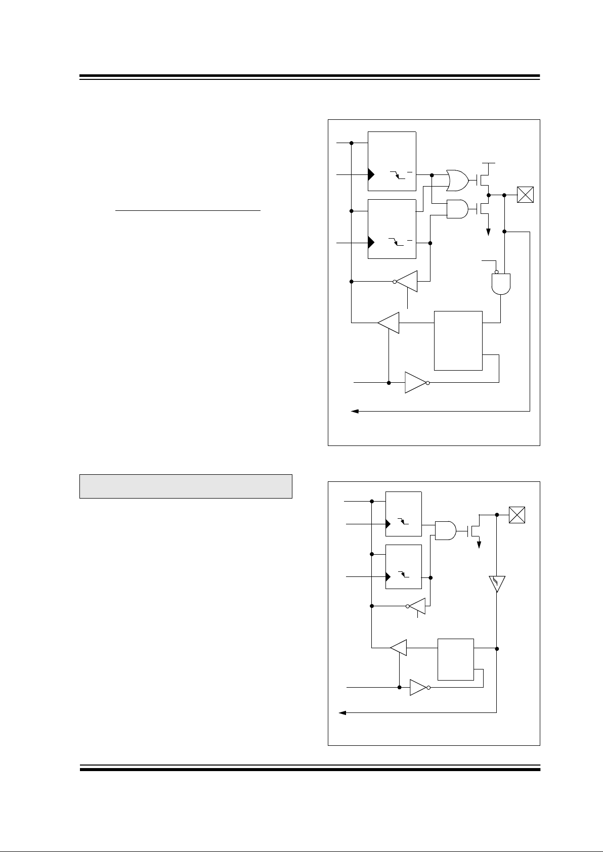
FIGURE 3-1: BLOCK DIAGRAM OF
RA3:RA0 AND RA5 PINS
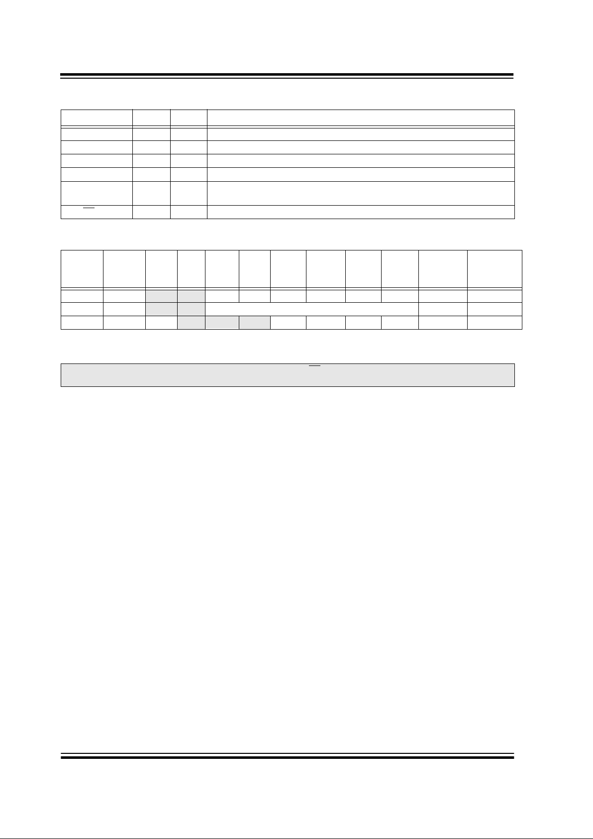
FIGURE 3-2: BLOCK DIAGRAM OF RA4/
T0CKI PIN
Note: On a Power-on Reset, these pins are con-
figured as analog inputs and read as '0'.
Data
Bus
QD
Q
CK
QD
Q
CK
QD
EN
P
N
WR
Port
WR
TRIS
Data Latch
TRIS Latch
RD TRIS
RD PORT
V
SS
VDD
I/O pin
(1)
Note 1: I/O pins have protection diodes to VDD and VSS.
Analog
Input
Mode
TTL
Input
Buffer
To A/D Converter
Data
Bus
WR
PORT
WR
TRIS
RD PORT
Data Latch
TRIS Latch
RD TRIS
Schmitt
Trigger
Input
Buffer
N
V
SS
I/O pin
(1)
TMR0 clock input
QD
Q
CK
QD
Q
CK
EN
QD
EN
Note 1: I/O pin has protection diodes to VSS only.
PIC16F87X
DS30292B-page 30
1999 Microchip Technology Inc.
TABLE 3-1: PORTA FUNCTIONS
TABLE 3-2: SUMMARY OF REGISTERS ASSOCIATED WITH PORTA
Name Bit# Buffer Function
RA0/AN0 bit0 TTL Input/output or analog inp ut
RA1/AN1 bit1 TTL Input/output or analog inp ut
RA2/AN2 bit2 TTL Input/output or analog inp ut
RA3/AN3/VREF bit3 TTL Input/output or analog input or VREF
RA4/T0CKI bit4 ST Input/output or external clock input for Timer0
Output is open drain type
RA5/SS
/AN4 bit5 TTL Input/output or slave select input for synchronous serial port or analog input
Legend: TTL = TTL input, ST = Schmitt Trigger input
Address Name Bit 7 Bit 6 Bit 5 Bit 4 Bit 3 Bit 2 Bit 1 Bit 0
Value on:
POR,
BOR
Value on all
other
resets
05h PORT A — — RA5 RA4 RA3 RA2 RA1 RA0
--0x 0000 --0u 0000
85h TRISA — — PORTA Data Direction Register
--11 1111 --11 1111
9Fh ADCON1 ADFM — — — PCFG3 PCFG2 PCFG1 PCFG0
--0- 0000 --0- 0000
Legend: x = unkno wn, u = unchanged, - = unimplemented locations read as '0'. Shaded cells are not used by PORTA.
Note: When using the SSP module in SPI slave mode and SS enabled, the A/D converter must be set to one of
the following modes where PCFG3:PCFG0 = 0100,0101, 011x, 1101, 1110, 1111.
 Loading...