

Datasheet PIC16F873-04-L, PIC16F873-04-P, PIC16F873-04-PQ, PIC16F873-04-PT, PIC16F873-04-SO Datasheet (Microchip Technology)
...
2001 Microchip Technology Inc. DS30292C
PIC16F87X
Data Sheet
28/40-Pin 8-Bit CMOS FLASH
Microcontrollers

DS30292C - page ii 2001 Microchip Technology Inc.
“All rights reserved. Copyright © 2001, Microchip Technology
Incorporated, USA. Information contained in this publication
regarding device applications and the like is intended through
suggestion only and may be superseded by updates. No representation or warranty is given and no liability is assumed by
Microchip Technology Incorporated with respect to the accuracy or use of such information, or infringement of patents or
other intellectual property rights arising from such use or ot herwise. Use of Microchip’s products as critical components in
life support systems is not authorized except with express
written approval by Microchip. No licenses are conveyed,
implicitly or otherwise, under any intellectual property rights.
The Microchip logo and name are registered trademarks of
Microchip Technology Inc. in the U.S.A. and other countries.
All rights reserved. All other trademarks mentioned herein are
the property of their respective companies. No licenses are
conveyed, implicitly or otherwise, under any intellectual property rights.”
Trademarks
The Microchip name, logo, PIC, PICmicro, PICMASTER, PICSTART, PRO MATE, K
EELOQ, SEEVAL, MPLAB and The
Embedded Control Solutions Company are registered trademarks of Microchip Technology Incorporated in the U.S.A. and
other countries.
Total Endurance, ICSP, In-Circuit Serial Programming, FilterLab, MXDEV, microID, FlexROM, fuzzyLAB, MPASM,
MPLINK, MPLIB, PICDEM, ICEPIC, Migratable Memory,
FanSense, ECONOMONITOR and SelectMode are trademarks of Microchip Technology Incorporated in the U.S.A.
Serialized Quick T erm Programming (SQTP) is a service mark
of Microchip Technology Incorporated in the U.S.A.
All other trademarks mentioned herein are property of their
respective companies.
© 2001, Microchip Technology Incorporated, Printed in the
U.S.A., All Rights Reserved.
Microchip received QS-9000 quality system
certification for its worldwide headquarters,
design and wafer fabrication facilities in
Chandler and Tempe, Arizona in July 1999. The
Company’s quality system processes and
procedures are QS-9000 compliant for its
PICmicro
®
8-bit MCUs, KEELOQ
®
code hoppin g
devices, Serial EEPROMs and microperipheral
products. In addition, Microchip’s quality
system for the design and manufacture of
development systems is ISO 9001 certified.
2001 Microchip Technology Inc. DS30292C-page 1
PIC16F87X
Devices Included in this Data Sheet:
Microcontroller Core Features:
• High performance RISC CPU
• Only 35 single word instructions to learn
• All single cycle instructions except for program
branches which are two cycle
• Operating speed: DC - 20 MHz clock input
DC - 200 ns instruction cycle
• Up to 8K x 14 words of FLASH Program M em ory,
Up to 368 x 8 bytes of Data Memory (RAM)
Up to 256 x 8 bytes of EEPROM Data Memory
• Pinout compatible to the PIC16C73B/74B/76/77
• Interrupt capability (up to 14 sources)
• Eight level deep hardware stack
• Direct, indirect and relative addressing modes
• Power-on Reset (POR)
• Power-up Timer (PWRT) and
Oscillator Start-up Timer (OST)
• Watchdog Timer (WDT) with its own on-chip RC
oscillator for reliable operation
• Programmable code protection
• Power saving SLEEP mode
• Selectable oscillator options
• Low power, high speed CMOS FLASH/EEPROM
technology
• Fully static design
• In-Circuit Serial Programming (ICSP) via two
pins
• Single 5V In-Circuit Seria l Programming capability
• In-Circuit Debugging via two pins
• Processor read/write access to program memory
• Wide operating voltage range: 2.0V to 5.5V
• High Sink/Source Current: 25 mA
• Commercial, Industria l and Extended temp erature
ranges
• Low-power consumption:
- < 0.6 mA typical @ 3V, 4 MHz
-20 µA typical @ 3V, 32 kHz
-< 1 µA typical standby current
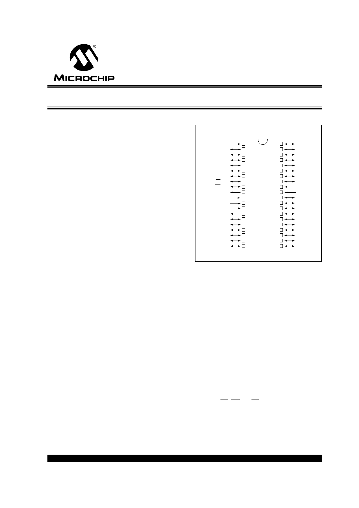
Pin Diagram
Peripheral Features:
• Timer0: 8-bit timer/counter with 8-bit prescaler
• Timer1: 16-bit timer/counter with prescaler,
can be incremented during SLEEP via external
crystal/clock
• Timer2: 8-bit timer/counter with 8-bit period
register, prescaler and postscaler
• Two Capture, Compare, PWM modules
- Capture is 16-bit, max. resolution is 12.5 ns
- Compare is 16-bit, max. resolution is 200 ns
- PWM max. resolution is 10-bit
• 10-bit multi-channel Analog-to-Digital converter
• Synchronous Serial Port (SSP) with SPI
(Master
mode) and I
2C
(Master/Slave)
• Universal Synchronous Asynchronous Receiver
Transmitter (USART/SCI) with 9-bit address
detection
• Parallel Slave Port (PSP) 8-bits wide, with
external RD
, WR and CS controls (40/44-pin only)
• Brown-out detection circuitry for
Brown-out Reset (BOR)
• PIC16F873
• PIC16F874
• PIC16F876
• PIC16F877
RB7/PGD
RB6/PGC
RB5
RB4
RB3/PGM
RB2
RB1
RB0/INT
VDD
VSS
RD7/PSP7
RD6/PSP6
RD5/PSP5
RD4/PSP4
RC7/RX/DT
RC6/TX/CK
RC5/SDO
RC4/SDI/SDA
RD3/PSP3
RD2/PSP2
MCLR/VPP
RA0/AN0
RA1/AN1
RA2/AN2/VREF-
RA3/AN3/VREF+
RA4/T0CKI
RA5/AN4/SS
RE0/RD/AN5
RE1/WR/AN6
RE2/CS/AN7
VDD
VSS
OSC1/CLKIN
OSC2/CLKOUT
RC0/T1OSO/T1CKI
RC1/T1OSI/CCP2
RC2/CCP1
RC3/SCK/SCL
RD0/PSP0
RD1/PSP1
1
2
3
4
5
6
7
8
9
10
11
12
13
14
15
16
17
18
19
20
40
39
38
37
36
35
34
33
32
31
30
29
28
27
26
25
24
23
22
21
PIC16F877/874
PDIP
28/40-Pin 8-Bit CMOS FLASH Microcontrollers
PIC16F87X
DS30292C-page 2 2001 Microchip Technology Inc.
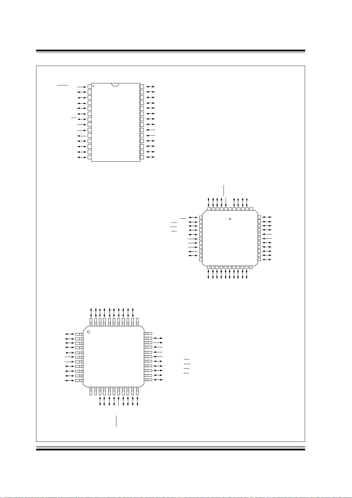
Pin Diagrams
PIC16F876/873
10
11
2
3
4
5
6
1
8
7
9
12
13
14
15
16
17
18
19
20
23
24
25
26
27
28
22
21
MCLR/VPP
RA0/AN0
RA1/AN1
RA2/AN2/V
REF-
RA3/AN3/V
REF+
RA4/T0CKI
RA5/AN4/SS
VSS
OSC1/CLKIN
OSC2/CLKOUT
RC0/T1OSO/T1CKI
RC1/T1OSI/CCP2
RC2/CCP1
RC3/SCK/SCL
RB7/PGD
RB6/PGC
RB5
RB4
RB3/PGM
RB2
RB1
RB0/INT
V
DD
VSS
RC7/RX/DT
RC6/TX/CK
RC5/SDO
RC4/SDI/SDA
10
11
12
13
14
15
16
17
181920212223242526
44
8
7
65432
1
27
28
29
30
31
32
33
34
35
36
37
38
39
40
41
42
43
9
PIC16F877
RA4/T0CKI
RA5/AN4/SS
RE0/RD/AN5
OSC1/CLKIN
OSC2/CLKOUT
RC0/T1OSO/T1CK1
NC
RE1/WR
/AN6
RE2/CS
/AN7
V
DD
VSS
RB3/PGM
RB2
RB1
RB0/INT
V
DD
VSS
RD7/PSP7
RD6/PSP6
RD5/PSP5
RD4/PSP4
RC7/RX/DT
RA3/AN3/VREF+
RA2/AN2/V
REF-
RA1/AN1
RA0/AN0
MCLR
/VPP
NC
RB7/PGD
RB6/PGC
RB5
RB4
NC
NC
RC6/TX/CK
RC5/SDO
RC4/SDI/SDA
RD3/PSP3
RD2/PSP2
RD1/PSP1
RD0/PSP0
RC3/SCK/SCL
RC2/CCP1
RC1/T1OSI/CCP2
10
11
2
3
4
5
6
1
1819202122
121314
15
38
8
7
4443424140
39
16
17
29
30
31
32
33
23
24
25
26
27
28
363435
9
PIC16F877
37
RA3/AN3/VREF+
RA2/AN2/V
REF-
RA1/AN1
RA0/AN0
MCLR
/VPP
NC
RB7/PGD
RB6/PGC
RB5
RB4
NC
RC6/TX/CK
RC5/SDO
RC4/SDI/SDA
RD3/PSP3
RD2/PSP2
RD1/PSP1
RD0/PSP0
RC3/SCK/SCL
RC2/CCP1
RC1/T1OSI/CCP2
NC
NC
RC0/T1OSO/T1CKI
OSC2/CLKOUT
OSC1/CLKIN
V
SS
VDD
RE2/AN7/CS
RE1/AN6/WR
RE0/AN5/RD
RA5/AN4/SS
RA4/T0CKI
RC7/RX/DT
RD4/PSP4
RD5/PSP5
RD6/PSP6
RD7/PSP7
V
SS
VDD
RB0/INT
RB1
RB2
RB3/PGM
PLCC
QFP
PDIP, SOIC
PIC16F874
PIC16F874

2001 Microchip Technology Inc. DS30292C-page 3
PIC16F87X
Key Features
PICmicro™ Mid-Range Reference
Manual (DS3 3023)
PIC16F873 PIC16F874 PIC16F876 PIC16F877
Operating Frequency DC - 20 MHz DC - 20 MHz DC - 20 MHz DC - 20 MHz
RESETS (and Delays) POR, BOR
(PWRT, OST)
POR, BOR
(PWRT, OST)
POR, BOR
(PWRT, OST)
POR, BOR
(PWRT, OST)
FLASH Program Memory
(14-bit words)
4K 4K 8K 8K
Data Memory (bytes) 192 192 368 368
EEPROM Data Memory 128 128 256 256
Interrupts 13 14 13 14
I/O Ports Ports A,B,C Ports A,B,C,D,E Ports A,B,C Ports A,B,C,D,E
Timers 3333
Capture/Compa re/PW M Mo dul es 2 2 2 2
Serial Communications MSSP, USART MSSP, USART MSSP, USART MSSP, USART
Parallel Communications — PSP — PSP
10-bit Analog-to-Digital Module 5 input channels 8 input channels 5 input channels 8 input channels
Instruction Set 35 instructions 35 instructions 35 instructions 35 instructions

PIC16F87X
DS30292C-page 4 2001 Microchip Technology Inc.
Table of Contents
1.0 Device Overview................................................................................................................................................... 5
2.0 Memory Organization.......................................................................................................................................... 11
3.0 I/O Ports.............................................................................................................................................................. 29
4.0 Data EEPROM and FLASH Program Memory.................................................................................................... 41
5.0 Timer0 Module.................................................................................................................................................... 47
6.0 Timer1 Module.................................................................................................................................................... 51
7.0 Timer2 Module.................................................................................................................................................... 55
8.0 Capture/Compare/PWM Modules....................................................................................................................... 57
9.0 Master Synchronous Serial Port (MSSP) Module............................................................................................... 65
10.0 Addressable Universal Synchronous Asynchronous Receiver Transmitter (USART) ........................................ 95
11.0 Analog-to-Digital Converter (A/D) Module......................................................................................................... 111
12.0 Special Features of the CPU............................................................................................................................. 119
13.0 Instruction Set Summary................................................................................................................................... 135
14.0 Development Support ....................................................... ...... ...... ..... ...... ......................................................... 143
15.0 Electrical Characteristics................................................................................................................................... 149
16.0 DC and AC Characteristics Graphs and Tables................................................................................................ 177
17.0 Packaging Information ...................................................................................................................................... 189
Appendix A: Revision History .................................................................................................................................... 197
Appendix B: Device Differences ................................................................................................................................ 197
Appendix C: Conversion Considerations................................................................................................................... 198
Index .......................................................................................................................................................................... 199
On-Line Support......................................................................................................................................................... 207
Reader Response...................................................................................................................................................... 208
PIC16F87X Product Identification System................................................................................................................. 209
TO OUR VALUED CUSTOMERS
It is our intention to provide our valued customers with the best documentation possible to ensure successful use of your Microchip
products. To this end, we will continue to improve our publications to better suit your needs. Our publications will be refined and
enhanced as new volumes and updates are introduced.
If you have any questions or co mm ents regarding this publication, please contact the Marketing Communications Department via
E-mail at docerrors@mail.microchip.com or fax the Reader Response Form in the back of this data sheet to (480) 792-4150.
We welcome your feedback.
Most Current Data Sheet
To obtain the most up-to-date version of this data sheet, please register at our Worldwide Web site at:
http://www.microchip.com
You can determine the version of a data sheet by examining its literature number found on the bottom outside corner of any page.
The last character of the literature number is the version number, (e.g., DS30000A is version A of document DS30000).
Errata
An errata sheet, describing minor operational differences from the data sheet and recommended workarounds, may exist for current
devices. As device/documentation issues become known to us, we will publish an errata sheet. The errata will specify the revision
of silicon and revision of document to which it applies.
To determine if an errata sheet exists for a particular device, please check with one of the following:
• Microchip’s Worldwide Web site; http://www.microchip.com
• Your local Microchip sales office (see last page)
• The Microchip Corporate Literature Center; U.S. FAX: (480) 792-7277
When contacting a sales office or the literature center, please specify which device, revision of silicon and data sheet (include literature number) you are using.
Customer Notification System
Register on our web site at www.microchip.com/cn to receive the most current information on all of our products.
2001 Microchip Technology Inc. DS30292C-page 5
PIC16F87X
1.0 DEVICE OVERVIEW
This document contains device specific information.
Additional information may be found in the PICmicro™
Mid-Range Reference Manual (DS33023), which may
be obtained from your local Microchip Sales Representative or downloaded from the Microchip website. The
Reference Manual should be considered a complementary document to this data sheet, and is highly recommended reading for a better understanding of the device
architecture and operation of the peripheral modules.
There are four devices (PIC16F873, PIC16F874,
PIC16F876 and PIC16F877) covered by this data
sheet. The PIC16F876/873 devices come in 28-pin
packages and the PIC16F877/874 devices come in
40-pin packages. The Parallel Slave Port is not
implemented on the 28-pin devic es .
The following device bloc k diagrams are s orted by pin
number; 28-pin for Figure 1-1 and 40-pin for Figure 1-2.
The 28-pin and 40-pin pin outs are listed in Table 1- 1
and Table 1-2, respectively.
FIGURE 1-1: PIC16F873 AND PIC16F876 BLOCK DIAGRAM
FLASH
Program
Memory
13
Data Bus
8
14
Program
Bus
Instruction reg
Program Counter
8 Level Stack
(13-bit)
RAM
File
Registers
Direct Addr
7
RAM Addr
(1)
9
Addr MUX
Indirect
Addr
FSR reg
STATUS reg
MUX
ALU
W reg
Power-up
Timer
Oscillator
Start-up Timer
Power-on
Reset
Watchdog
Timer
Instruction
Decode &
Control
Timing
Generation
OSC1/CLKIN
OSC2/CLKOUT
MCLR
VDD, VSS
PORTA
PORTB
PORTC
RA4/T0CKI
RA5/AN4/SS
RB0/INT
RC0/T1OSO/T1CKI
RC1/T1OSI/CCP2
RC2/CCP1
RC3/SCK/SCL
RC4/SDI/SDA
RC5/SDO
RC6/TX/CK
RC7/RX/DT
8
8
Brown-out
Reset
Note 1: Higher order bits are from the STATUS register.
USART
CCP1,2
Synchronous
10-bit A/DTimer0 Timer1 Timer2
Serial Port
RA3/AN3/VREF+
RA2/AN2/VREF-
RA1/AN1
RA0/AN0
8
3
Data EEPROM
RB1
RB2
RB3/PGM
RB4
RB5
RB6/PGC
RB7/PGD
Device
Program
FLASH
Data Memory
Data
EEPROM
PIC16F873 4K 192 Bytes 128 Bytes
PIC16F876 8K 368 Bytes 256 Bytes
In-Circuit
Debugger
Low Voltage
Programming
PIC16F87X
DS30292C-page 6 2001 Microchip Technology Inc.
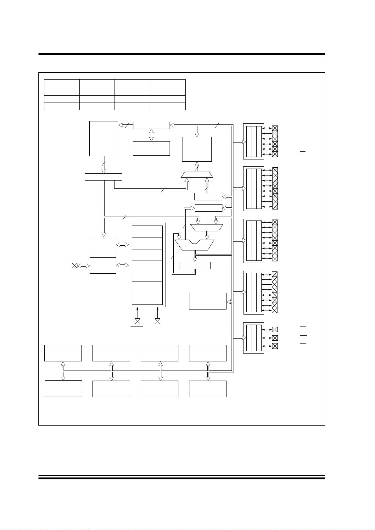
FIGURE 1-2: PIC16F874 AND PIC16F877 BLOCK DIAGRAM
FLASH
Program
Memory
13
Data Bus
8
14
Program
Bus
Instruction reg
Program Counter
8 Level Stack
(13-bit)
RAM
File
Registers
Direct Addr
7
RAM Addr
(1)
9
Addr MUX
Indirect
Addr
FSR reg
STATUS reg
MUX
ALU
W reg
Power-up
Timer
Oscillator
Start-up Timer
Power-on
Reset
Watchdog
Timer
Instruction
Decode &
Control
Timing
Generation
OSC1/CLKIN
OSC2/CLKOUT
MCLR
VDD, VSS
PORTA
PORTB
PORTC
PORTD
PORTE
RA4/T0CKI
RA5/AN4/SS
RC0/T1OSO/T1CKI
RC1/T1OSI/CCP2
RC2/CCP1
RC3/SCK/SCL
RC4/SDI/SDA
RC5/SDO
RC6/TX/CK
RC7/RX/DT
RE0/AN5/RD
RE1/AN6/WR
RE2/AN7/CS
8
8
Brown-out
Reset
Note 1: Higher order bits are from the STATUS register.
USART
CCP1,2
Synchronous
10-bit A/DTimer0 Timer1 Timer2
Serial Port
RA3/AN3/VREF+
RA2/AN2/VREF-
RA1/AN1
RA0/AN0
Parallel Slave Port
8
3
Data EEPROM
RB0/INT
RB1
RB2
RB3/PGM
RB4
RB5
RB6/PGC
RB7/PGD
Device
Program
FLASH
Data Memory
Data
EEPROM
PIC16F874 4K 192 Bytes 128 Bytes
PIC16F877 8K 368 Bytes 256 Bytes
In-Circuit
Debugger
Low-Voltage
Programming
RD0/PSP0
RD1/PSP1
RD2/PSP2
RD3/PSP3
RD4/PSP4
RD5/PSP5
RD6/PSP6
RD7/PSP7

2001 Microchip Technology Inc. DS30292C-page 7
PIC16F87X
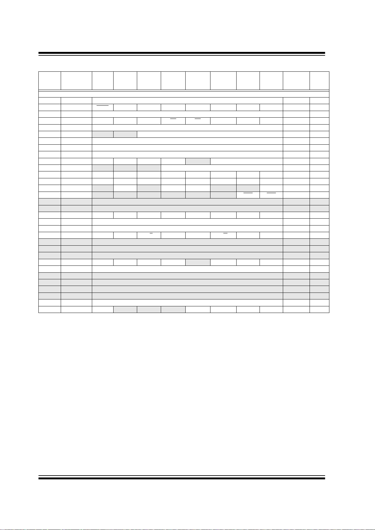
T ABLE 1-1: PIC16F873 AND PIC16F876 PINOUT DESCRIPTION
Pin Name
DIP
Pin#
SOIC
Pin#
I/O/P
Type
Buffer
Type
Description
OSC1/CLKIN 9 9 I ST/CMOS
(3)
Oscillator crystal input/external clock source input.
OSC2/CLKOUT 10 10 O — Oscillator crystal output. Connects to crystal or resonator in
crystal oscillator mode. In RC mode, the OSC2 pin outputs
CLKOUT which has 1/4 the frequency of OSC1, and denotes
the instruction cycle rate.
MCLR
/VPP 1 1 I/P ST Master Clear (Reset) input or programming voltage input. This
pin is an active low RESET to the device.
PORTA is a bi-directional I/O port.
RA0/AN0 2 2 I/O TTL RA0 can also be analog input0.
RA1/AN1 3 3 I/O TTL RA1 can also be analog input1.
RA2/AN2/V
REF- 4 4 I/O TTL RA2 can also be analog input2 or negative analog
reference voltage.
RA3/AN3/V
REF+ 5 5 I/O TTL RA3 can also be analog input3 or positive analog
reference voltage.
RA4/T0CKI 6 6 I/O ST RA4 can also be the clock input to the Timer0
module. Output is open drain type.
RA5/SS
/AN4 7 7 I/O TTL RA5 can also be analog input4 or the slave select
for the synchronous serial port.
PORTB is a bi-directional I/O port. PORTB can be software
programmed for internal weak pull-up on all inputs.
RB0/INT 21 21 I/O TTL/ST
(1)
RB0 can also be the external interrupt pin.
RB1 22 22 I/O TTL
RB2 23 23 I/O TTL
RB3/PGM 24 24 I/O TTL RB3 can also be the low voltage programming input.
RB4 25 25 I/O TTL Interrupt-on-change pin.
RB5 26 26 I/O TTL Interrupt-on-change pin.
RB6/PGC 27 27 I/O TTL/ ST
(2)
Interrupt-on-change pin or In-Circuit Debugger pin. Serial
programming clock.
RB7/PGD 28 28 I/O TTL/ ST
(2)
Interrupt-on-change pin or In-Circuit Debugger pin. Serial
programming data.
PORTC is a bi-directional I/O port.
RC0/T1OSO/T1CKI 11 11 I/O ST RC0 can also be the Timer1 oscillator output or Timer1
clock input.
RC1/T1OSI/CCP2 12 12 I/O ST RC1 can also be the Timer1 oscillator input or Capture2
input/Compare2 output/PWM2 output.
RC2/CCP1 13 13 I/O ST RC2 can also be the Capture1 input/Compare1 output/
PWM1 output.
RC3/SCK/SCL 14 14 I/O ST RC3 can also be the synchronous serial clock input/output
for both SPI and I
2
C modes.
RC4/SDI/SDA 15 15 I/O ST RC4 can also be the SPI Data In (SPI mode) or
data I/O (I
2
C mode).
RC5/SDO 16 16 I/O ST RC5 can also be the SPI Data Out (SPI mode).
RC6/TX/CK 17 17 I/O ST RC6 can also be the USART Asynchronous Transmit or
Synchronous Clock.
RC7/RX/DT 18 18 I/O ST RC7 can also be the USART Asynchronous Rece ive or
Synchronous Data.
V
SS 8, 19 8, 19 P — Ground reference for logic and I/O pins.
V
DD 20 20 P — Positive supply for logic and I/O pins.
Legend: I = input O = output I/O = input/output P = power
— = Not used TTL = TTL input ST = Schmitt Trigger input
Note 1: This buffer is a Schmitt Trigger input when configured as the external interrupt.
2: This buffer is a Schmitt Trigger input when used in Serial Programming mode.
3: This buffer is a Schmitt Trigger input when configured in RC oscillator mode and a CMOS input otherwise.

PIC16F87X
DS30292C-page 8 2001 Microchip Technology Inc.
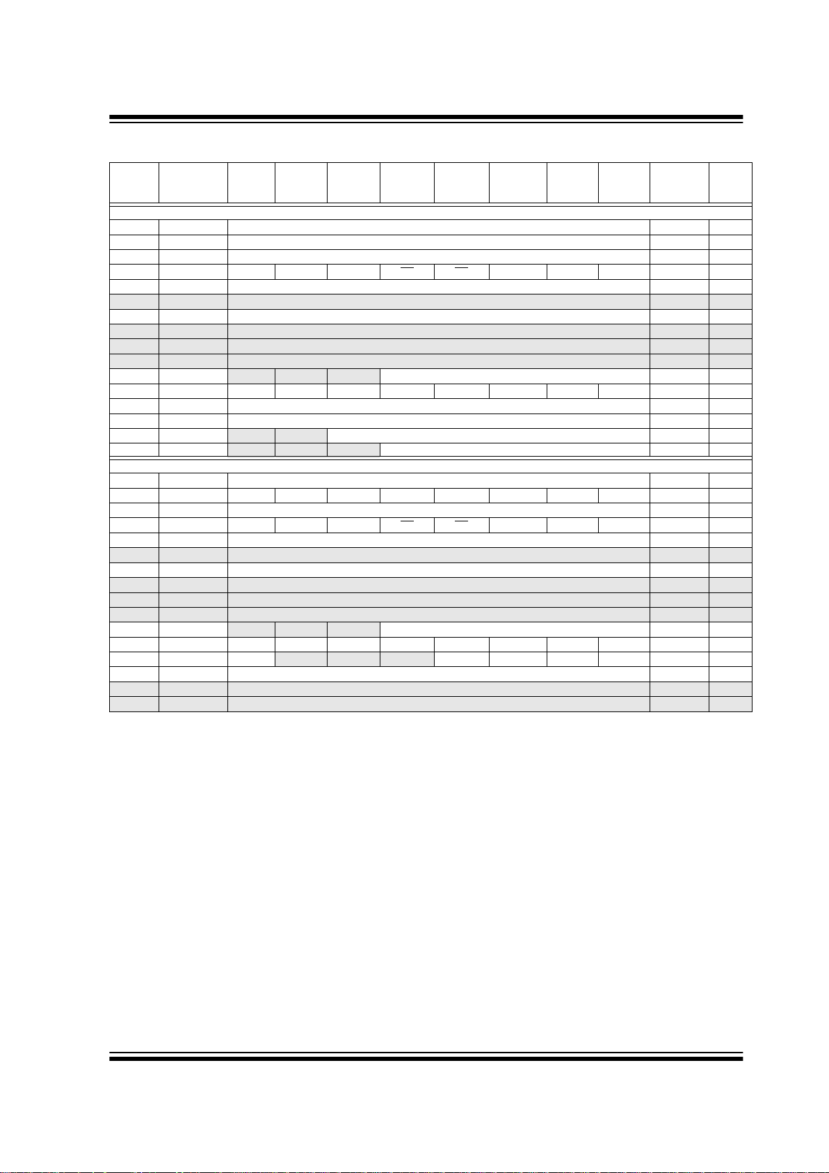
TABLE 1-2: PIC16F874 AND PIC16F877 PINOUT DESCRIPTION
Pin Name
DIP
Pin#
PLCC
Pin#
QFP
Pin#
I/O/P
Type
Buffer
Type
Description
OSC1/CLKIN 13 14 30 I ST/CMOS
(4)
Oscillator crystal input/external clock source input.
OSC2/CLKOUT 14 15 31 O — Oscillator crystal output. Connects to crystal or resonator
in crystal oscillator mode. In RC mode, OSC2 pin outputs
CLKOUT which has 1/4 the frequency of OSC1, and
denotes the instruction cycle rate.
MCLR
/VPP 1 2 18 I/P ST Master Clear (Reset) input or programming voltage input.
This pin is an active low RESET to the device.
PORTA is a bi-directional I/O port.
RA0/AN0 2 3 19 I/O TTL RA0 can also be analog input0.
RA1/AN1 3 4 20 I/O TTL RA1 can also be analog input1.
RA2/AN2/V
REF- 4 5 21 I/O TTL RA2 can also be analog input2 or negative
analog reference voltage.
RA3/AN3/V
REF+ 5 6 22 I/O TTL RA3 can also be analog input3 or positive
analog reference voltage.
RA4/T0CKI 6 7 23 I/O ST RA4 can also be the clock input to the Timer0 timer/
counter. Output is open drain type.
RA5/SS/
AN4 7 8 2 4 I/O TTL RA5 can also be analog input4 or the slave select for
the synchronous serial port.
PORTB is a bi-directional I/O port. PORTB can be soft-
ware programmed for internal weak pull-up on all inputs.
RB0/INT 33 36 8 I/O TTL/ST
(1)
RB0 can also be the external interrupt pin.
RB1 34 37 9 I/O TTL
RB2 35 38 10 I/O TTL
RB3/PGM 36 39 11 I/O TTL RB3 can also be the low voltage programming input.
RB4 37 41 14 I/O TTL Interrupt-on-change pin.
RB5 38 42 15 I/O TTL Interrupt-on-change pin.
RB6/PGC 39 43 16 I/O TTL/ST
(2)
Interrupt-on-change pin or In-Circuit Debugger pin.
Serial programming clock.
RB7/PGD 40 44 17 I/O TTL/ST
(2)
Interrupt-on-change pin or In-Circuit Debugger pin.
Serial programming data.
Legend: I = input O = output I/O = input/output P = power
— = Not used TTL = TTL input ST = Schmitt Trigger input
Note 1: This buffer is a Schmitt Trigger input when configured as an external interrupt.
2: This buffer is a Schmitt Trigger input when used in Serial Programming mode.
3: This buffer is a Schmitt Trigger input when configured as general purpose I/O and a TTL input when used in the Parallel
Slave Port mode (for interfacing to a microprocessor bus).
4: This buffer is a Schmitt Trigger input when configured in RC oscillator mode and a CMOS input otherwise.

2001 Microchip Technology Inc. DS30292C-page 9
PIC16F87X
PORTC is a bi-directional I/O port.
RC0/T1OSO/T1CKI 15 16 32 I/O ST RC0 can also be the Timer1 oscillator output or a
Timer1 clock input.
RC1/T1OSI/CCP2 16 18 35 I/O ST RC1 can also be the Timer1 oscillator input or
Capture2 input/Compare2 output/PWM2 output.
RC2/CCP1 17 19 36 I/O ST RC2 can also be the Capture1 input/Compare1
output/PWM1 output.
RC3/SCK/SCL 18 20 37 I/O ST RC3 can also be the synchronous serial clock input/
output for both SPI and I
2
C modes.
RC4/SDI/SDA 23 25 42 I/O ST RC4 can also be the SPI Data In (SPI mode) or
data I/O (I
2
C mode).
RC5/SDO 24 26 43 I/O ST RC5 can also be the SPI Data Out (SPI mode).
RC6/TX/CK 25 27 44 I/O ST RC6 can also be the USART Asynchronous Transmit
or Synchronous Clock.
RC7/RX/DT 26 29 1 I/O S T RC7 can also be the USART Asynchronous Receive
or Synchronous Data.
PORTD is a bi-directional I/O port or parallel slave port
when interfacing to a microprocessor bus.
RD0/PSP0 19 21 38 I/O ST/TTL
(3)
RD1/PSP1 20 22 39 I/O ST/TTL
(3)
RD2/PSP2 21 23 40 I/O ST/TTL
(3)
RD3/PSP3 22 24 41 I/O ST/TTL
(3)
RD4/PSP4 27 30 2 I/O ST/TTL
(3)
RD5/PSP5 28 31 3 I/O ST/TTL
(3)
RD6/PSP6 29 32 4 I/O ST/TTL
(3)
RD7/PSP7 30 33 5 I/O ST/TTL
(3)
PORTE is a bi-directional I/O port.
RE0/RD
/AN5 8 9 25 I/O ST/TTL
(3)
RE0 can also be read control for the parallel slave
port, or analog input5.
RE1/WR
/AN6 9 10 26 I/O ST/TTL
(3)
RE1 can also be write control for the parallel slave
port, or analog input6.
RE2/CS
/AN7 10 11 27 I/O ST/TTL
(3)
RE2 can also be select control for the parallel slave
port, or analog input7.
V
SS 12,31 13,34 6,29 P — Ground reference for logic and I/O pins.
V
DD 11,32 12,35 7,28 P — Positive supply for logic and I/O pins.
NC — 1,17,28,4012,13,
33,34
— These pins are not internally connected. These pins
should be left unconnected.
T ABLE 1-2: PIC16F874 AND PIC16F877 PINOUT DESCRIPTION (CONTINUED)
Pin Name
DIP
Pin#
PLCC
Pin#
QFP
Pin#
I/O/P
Type
Buffer
Type
Description
Legend: I = input O = output I/O = input/output P = power
— = Not used TTL = TTL input ST = Schmitt Trigger input
Note 1: This buffer is a Schmitt Trigger input when configured as an external interrupt.
2: This buffer is a Schmitt Trigger input when used in Serial Programming mode.
3: This buffer is a Schmitt Trigger input when configured as general purpose I/O and a TTL input when used in the Parallel
Slave Port mode (for interfacing to a microprocessor bus).
4: This buffer is a Schmitt Trigger input when configured in RC oscillator mode and a CMOS input otherwise.

PIC16F87X
DS30292C-page 10 2001 Microchip Technology Inc.
NOTES:
2001 Microchip Technology Inc. DS30292C-page 11
PIC16F87X
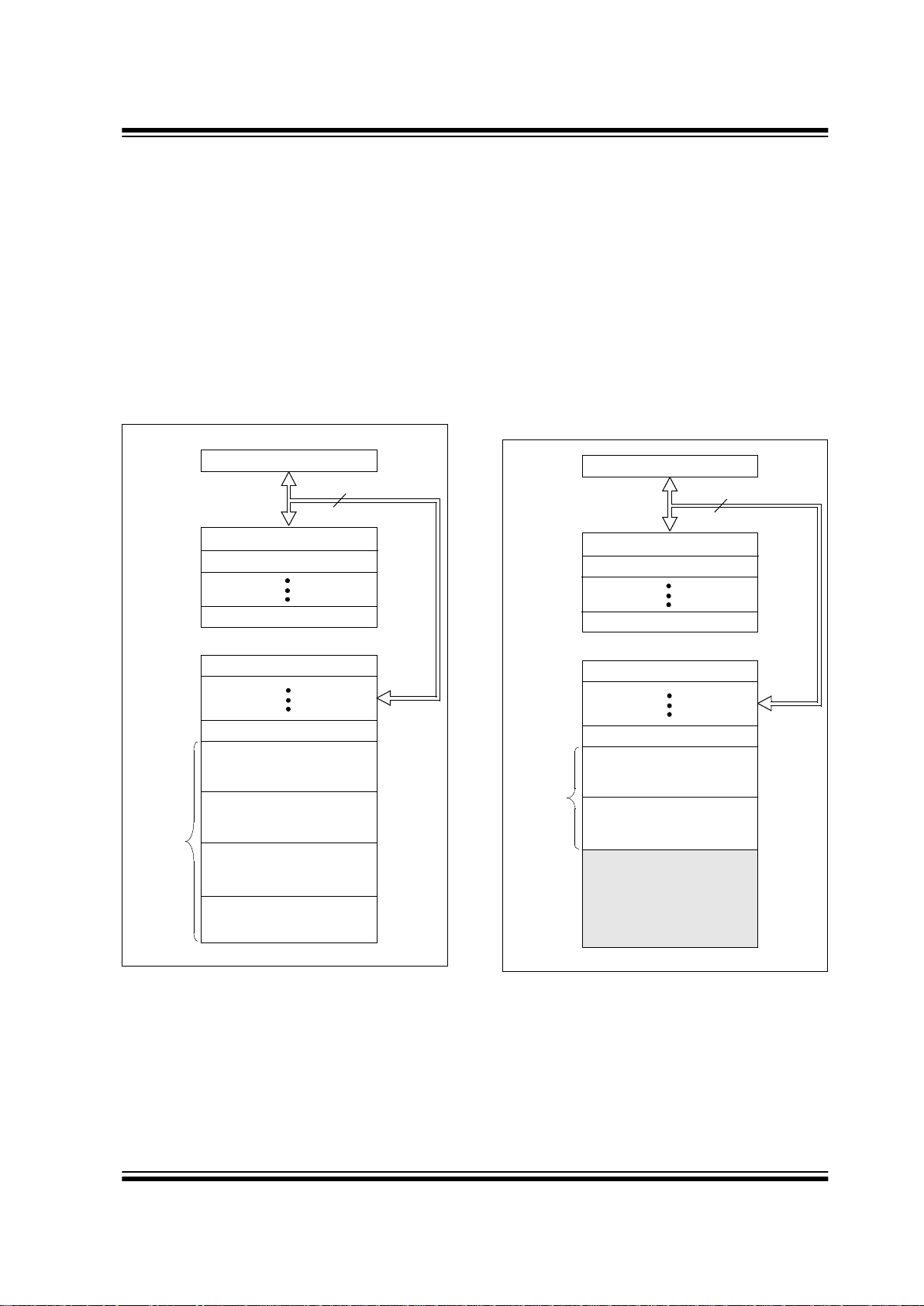
2.0 MEMORY ORGANIZATION
There are three memory blocks in each of the
PIC16F87X MCUs. The Program Memory and Data
Memory have separate buses so that concurrent
access can oc cur and is detailed in this section. T he
EEPROM data memory block is detailed in Se ction 4.0.
Additional informa tion on devi ce memory may be found
in the PICmicro Mid-Range Reference Manual,
(DS33023).
FIGURE 2-1: PIC16F877/876 PROGRAM
MEMORY MAP AND
STACK
2.1 Program Memory Organization
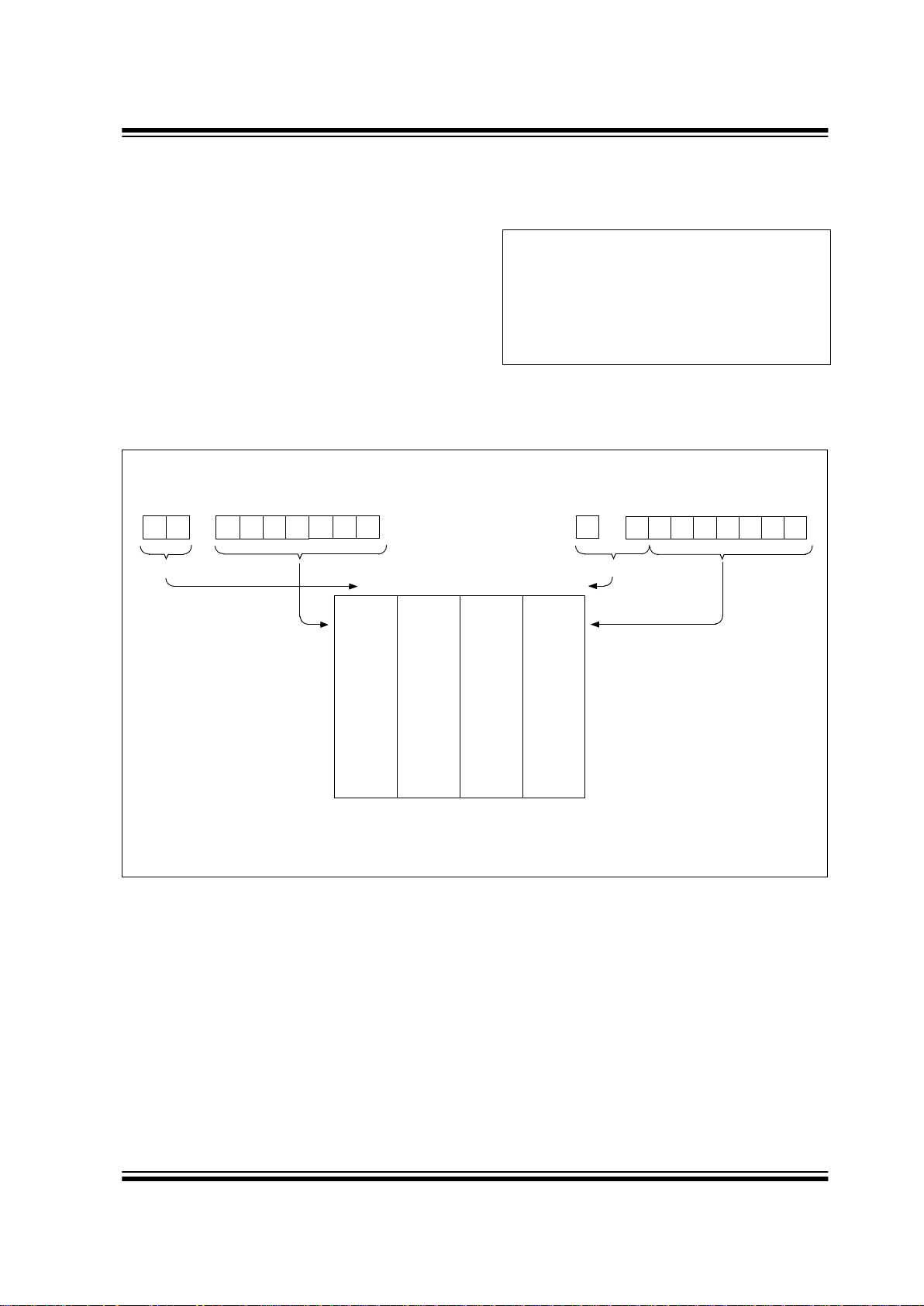
The PIC16F87X devic es have a 13-bit p rogram counter
capable of addressing an 8K x 14 program memory
space. The PIC16F877/876 devices have 8K x 14
words of FLASH program memory, and the
PIC16F873/874 devices have 4K x 14. Accessing a
location above the ph ysicall y implemente d address w ill
cause a wraparound.
The RESET vector is at 0000h and the interrupt vector
is at 0004h.
FIGURE 2-2: PIC16F874/873 PROGRAM
MEMORY MAP AND
STACK
PC<12:0>
13
0000h
0004h
0005h
Stack Level 1
Stack Level 8
RESET Vector
Interrupt Vector
On-Chip
CALL, RETURN
RETFIE, RETLW
1FFFh
Stack Level 2
Program
Memory
Page 0
Page 1
Page 2
Page 3
07FFh
0800h
0FFFh
1000h
17FFh
1800h
PC<12:0>
13
0000h
0004h
0005h
Stack Level 1
Stack Level 8
RESET Vector
Interrupt Vector
On-Chip
CALL, RETURN
RETFIE, RETLW
1FFFh
Stack Level 2
Program
Memory
Page 0
Page 1
07FFh
0800h
0FFFh
1000h

PIC16F87X
DS30292C-page 12 2001 Microchip Technology Inc.
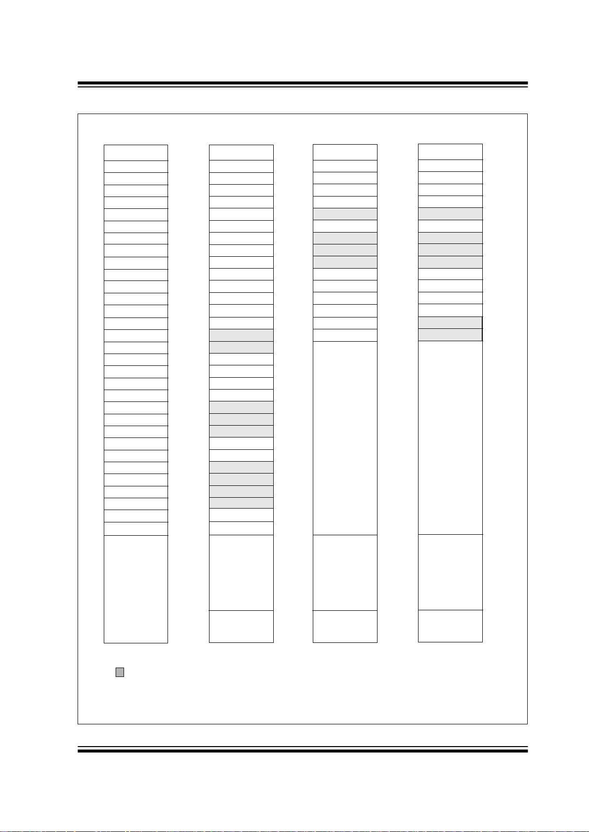
2.2 Data Memory Organization
The data memory is partitioned into multiple banks
which contain the General Purpose Registers and the
Special Function Registers. Bits RP1 (STATUS<6>)
and RP0 (STATUS<5>) are the bank select bits.
Each bank extends up to 7Fh (128 bytes). The lower
locations of each bank are reserved for the Special
Function Registers. Above the Special Function Registers are General Purpose Registers, implemented as
static RAM. All implemented banks contain Special
Function Registers. Some frequently used Special
Function Registers from one bank may be mirrored in
another bank for code reduction and quicker access.
2.2.1 GENERAL PURPOSE REGISTER
FILE
The register file can be acces sed either directly, or indirectly through the File Select Register (FSR).
RP1:RP0 Bank
00 0
01 1
10 2
11 3
Note: EEPROM Data Memory de scription can b e
found in Section 4.0 of this data sheet.
2001 Microchip Technology Inc. DS30292C-page 13
PIC16F87X
FIGURE 2-3: PIC16F877/876 REGISTER FILE MAP
Indirect addr.
(*)
TMR0
PCL
STATUS
FSR
PORTA
PORTB
PORTC
PCLATH
INTCON
PIR1
TMR1L
TMR1H
T1CON
TMR2
T2CON
SSPBUF
SSPCON
CCPR1L
CCPR1H
CCP1CON
OPTION_REG
PCL
ST ATUS
FSR
TRISA
TRISB
TRISC
PCLATH
INTCON
PIE1
PCON
PR2
SSPADD
SSPSTAT
00h
01h
02h
03h
04h
05h
06h
07h
08h
09h
0Ah
0Bh
0Ch
0Dh
0Eh
0Fh
10h
11h
12h
13h
14h
15h
16h
17h
18h
19h
1Ah
1Bh
1Ch
1Dh
1Eh
1Fh
80h
81h
82h
83h
84h
85h
86h
87h
88h
89h
8Ah
8Bh
8Ch
8Dh
8Eh
8Fh
90h
91h
92h
93h
94h
95h
96h
97h
98h
99h
9Ah
9Bh
9Ch
9Dh
9Eh
9Fh
20h
A0h
7Fh
FFh
Bank 0
Bank 1
Unimplemented data memory locations, read as ’0’.
* Not a physical register.
Note 1: These registers are not implemented on the PIC16F876.
2: These registers are reserved, maintain these registers clear.
File
Address
Indirect addr.
(*)
Indirect addr.
(*)
PCL
ST ATUS
FSR
PCLATH
INTCON
PCL
ST ATUS
FSR
PCLATH
INTCON
100h
101h
102h
103h
104h
105h
106h
107h
108h
109h
10Ah
10Bh
10Ch
10Dh
10Eh
10Fh
110h
111h
112h
113h
114h
115h
116h
117h
118h
119h
11Ah
11Bh
11Ch
11Dh
11Eh
11Fh
180h
181h
182h
183h
184h
185h
186h
187h
188h
189h
18Ah
18Bh
18Ch
18Dh
18Eh
18Fh
190h
191h
192h
193h
194h
195h
196h
197h
198h
199h
19Ah
19Bh
19Ch
19Dh
19Eh
19Fh
120h
1A0h
17Fh
1FFh
Bank 2
Bank 3
Indirect addr.
(*)
PORTD
(1)
PORTE
(1)
TRISD
(1)
ADRESL
TRISE
(1)
TMR0
OPTION_REG
PIR2
PIE2
RCST A
TXREG
RCREG
CCPR2L
CCPR2H
CCP2CON
ADRESH
ADCON0
TXSTA
SPBRG
ADCON1
General
Purpose
Register
General
Purpose
Register
General
Purpose
Register
General
Purpose
Register
1EFh
1F0h
accesses
70h - 7Fh
EFh
F0h
accesses
70h-7Fh
16Fh
170h
accesses
70h-7Fh
General
Purpose
Register
General
Purpose
Register
TRISB
PORTB
96 Bytes
80 Bytes 80 Bytes 80 Bytes
16 Bytes
16 Bytes
SSPCON2
EEDATA
EEADR
EECON1
EECON2
EEDATH
EEADRH
Reserved
(2)
Reserved
(2)
File
Address
File
Address
File
Address
File
Address
PIC16F87X
DS30292C-page 14 2001 Microchip Technology Inc.
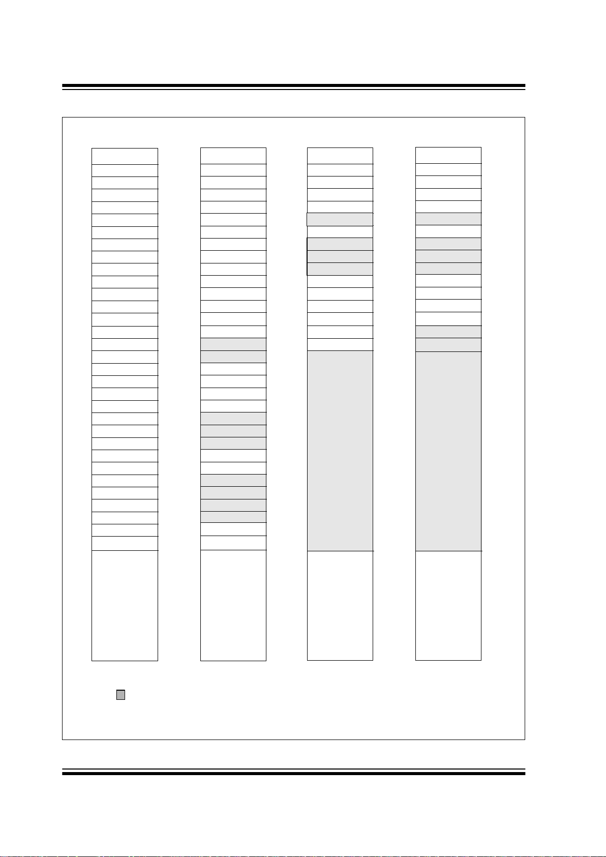
FIGURE 2-4: PIC16F874/873 REGISTER FILE MAP
Indirect addr.
(*)
TMR0
PCL
ST ATUS
FSR
PORTA
PORTB
PORTC
PCLATH
INTCON
PIR1
TMR1L
TMR1H
T1CON
TMR2
T2CON
SSPBUF
SSPCON
CCPR1L
CCPR1H
CCP1CON
OPTION_REG
PCL
ST ATUS
FSR
TRISA
TRISB
TRISC
PCLATH
INTCON
PIE1
PCON
PR2
SSPADD
SSPSTAT
00h
01h
02h
03h
04h
05h
06h
07h
08h
09h
0Ah
0Bh
0Ch
0Dh
0Eh
0Fh
10h
11h
12h
13h
14h
15h
16h
17h
18h
19h
1Ah
1Bh
1Ch
1Dh
1Eh
1Fh
80h
81h
82h
83h
84h
85h
86h
87h
88h
89h
8Ah
8Bh
8Ch
8Dh
8Eh
8Fh
90h
91h
92h
93h
94h
95h
96h
97h
98h
99h
9Ah
9Bh
9Ch
9Dh
9Eh
9Fh
20h
A0h
7Fh
FFh
Bank 0
Bank 1
Indirect addr.
(*)
Indirect addr.
(*)
PCL
STATUS
FSR
PCLATH
INTCON
PCL
STATUS
FSR
PCLATH
INTCON
100h
101h
102h
103h
104h
105h
106h
107h
108h
109h
10Ah
10Bh
180h
181h
182h
183h
184h
185h
186h
187h
188h
189h
18Ah
18Bh
17Fh
1FFh
Bank 2
Bank 3
Indirect addr.
(*)
PORTD
(1)
PORTE
(1)
TRISD
(1)
ADRESL
TRISE
(1)
TMR0
OPTION_REG
PIR2
PIE2
RCST A
TXREG
RCREG
CCPR2L
CCPR2H
CCP2CON
ADRESH
ADCON0
TXSTA
SPBRG
ADCON1
General
Purpose
Register
General
Purpose
Register
1EFh
1F0h
accesses
A0h - FFh
16Fh
170h
accesses
20h-7Fh
TRISB
PORTB
96 Bytes
96 Bytes
SSPCON2
10Ch
10Dh
10Eh
10Fh
110h
18Ch
18Dh
18Eh
18Fh
190h
EEDATA
EEADR
EECON1
EECON2
EEDATH
EEADRH
Reserved
(2)
Reserved
(2)
Unimplemented data memory locations, read as ’0’.
* Not a physical register.
Note 1: These registers are not implemented on the PIC16F873.
2: These registers are reserved, maintain these registers clear.
120h
1A0h
File
Address
File
Address
File
Address
File
Address
2001 Microchip Technology Inc. DS30292C-page 15
PIC16F87X
2.2.2 SPECIAL FUNCTION REGISTERS
The Special Function Registers are registers used by
the CPU and peripheral modules for controlling the
desired operation of the device. These registers are
implemented as static RAM. A list of these registers is
given in Table 2-1.
The Special Function Registers can be classified into
two sets: core (CPU) and peripheral. Those registers
associated with the core functions are described in
detail in this section. Those related to the operation of
the peripheral features are described in detail in the
peripheral features section.
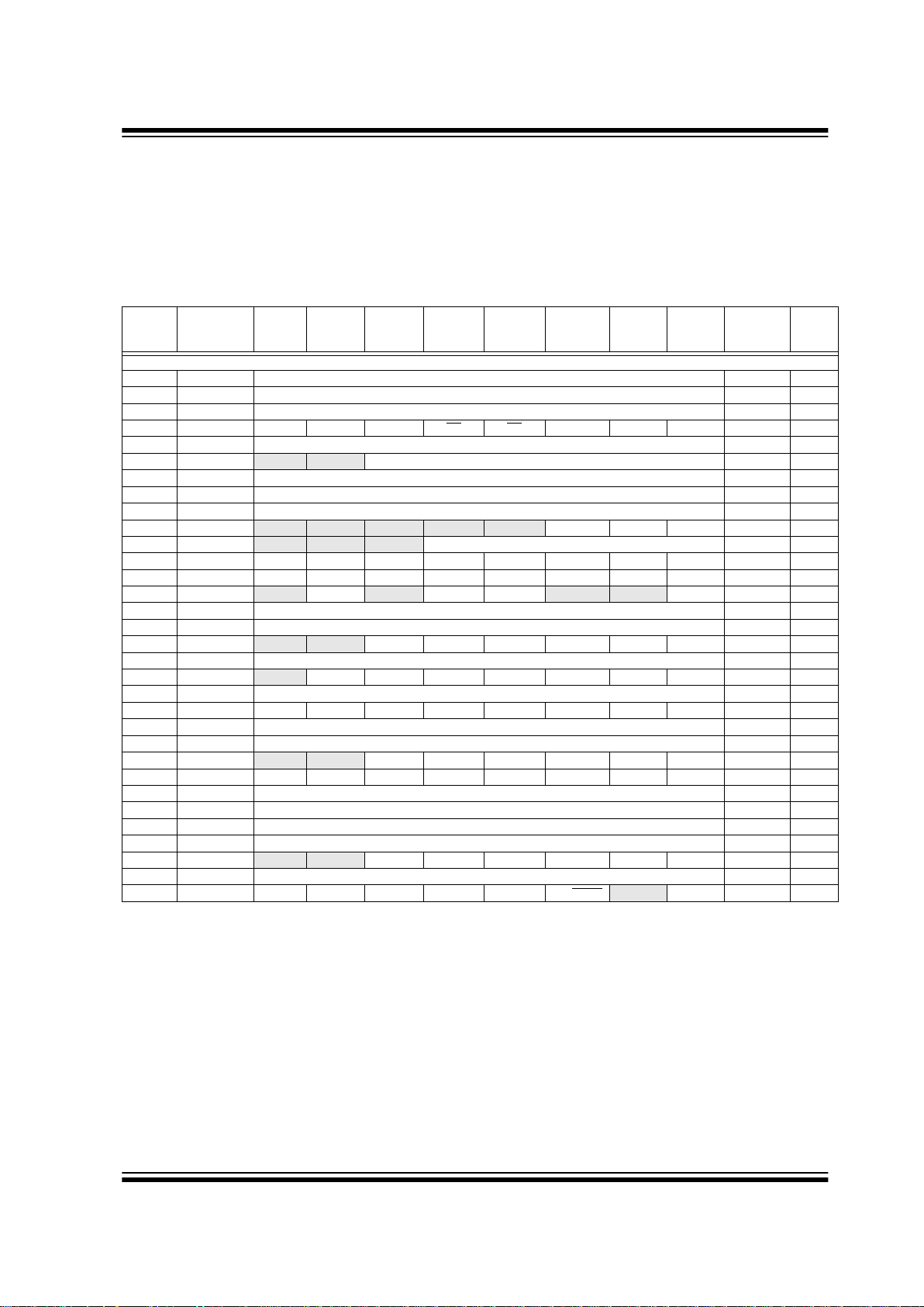
TABLE 2-1: SPECIAL FUNCTION REGISTER SUMMARY
Address Name Bit 7 Bit 6 Bit 5 Bit 4 Bit 3 Bit 2 Bit 1 Bit 0
Value on:
POR,
BOR
Details
on
page:
Bank 0
00h
(3)
INDF Addressing this location uses contents of FSR to address data memory (not a physical register) 0000 0000 27
01h TMR0 Timer0 Module Register
xxxx xxxx 47
02h
(3)
PCL Program Counter (PC) Least Significant Byte 0000 0000 26
03h
(3)
STATUS IRP RP1 RP0 TO PD ZDCC0001 1xxx 18
04h
(3)
FSR Indirect Data Memory Address Pointer xxxx xxxx 27
05h PORTA
— — PORTA Data Latch when written: PORTA pins when read --0x 0000 29
06h PORTB PORTB Data Latch when written: PORTB pins when read
xxxx xxxx 31
07h PORTC PORTC Data Latch when written: PORTC pins when read
xxxx xxxx 33
08h
(4)
PORTD PORTD Data Latch when written: PORTD pins when read xxxx xxxx 35
09h
(4)
PORTE — — — — — RE2 RE1 RE0 ---- -xxx 36
0Ah
(1,3)
PCLATH — — — Write Buffer for the upper 5 bits of the Program Counter ---0 0000 26
0Bh
(3)
INTCON GIE PEIE T0IE INTE RBIE T0IF INTF RBIF 0000 000x 20
0Ch PIR1 PSPIF
(3)
ADIF RCIF TXIF SSPIF CCP1IF TMR2IF TMR1IF 0000 0000 22
0Dh PIR2
— (5) — EEIF BCLIF — — CCP2IF -r-0 0--0 24
0Eh TMR1L Holding register for the Least Significant Byte of the 16-bit TMR1 Register
xxxx xxxx 52
0Fh TMR1H Holding register for the Most Significant Byte of the 16-bit TMR1 Register
xxxx xxxx 52
10h T1CON
— — T1CKPS1 T1CKPS0 T1OSCEN T1SYNC TMR1CS TMR1ON --00 0000 51
11h TMR2 Timer 2 Module Register
0000 0000 55
12h T2CON
— TOUTPS3 TOUTPS2 TOUTPS1 TOUTPS0 TMR2ON T2CKPS1 T2CKPS0 -000 0000 55
13h SSPBUF Synchronous Serial Port Rece i ve Buffer/Transmit Registe r
xxxx xxxx 70, 73
14h SSPCON WCOL SSPOV SSPEN CKP SSPM3 SSPM2 SSPM1 SSPM0
0000 0000 67
15h CCPR1L Capture/Compare/PWM Register1 (LSB)
xxxx xxxx 57
16h CCPR1H Capture/Compare/PWM Register1 (MSB)
xxxx xxxx 57
17h CCP1CON
— — CCP1X CCP1Y CCP1M3 CCP1M2 CCP1M1 CCP1M0 --00 0000 58
18h RCSTA SPEN RX9 SREN CREN ADDEN FERR OERR RX9D
0000 000x 96
19h TXREG USART Transmit Data Register
0000 0000 99
1Ah RCREG USART Receive Data Register
0000 0000 101
1Bh CCPR2L Capture/Compare/PWM Register2 (LSB)
xxxx xxxx 57
1Ch CCPR2H Capture/Compare/PWM Register2 (MSB)
xxxx xxxx 57
1Dh CCP2CON
— — CCP2X CCP2Y CCP2M3 CCP2M2 CCP2M1 CCP2M0 --00 0000 58
1Eh ADRESH A/D Result Register High Byte
xxxx xxxx 116
1Fh ADCON0 ADCS1 ADCS0 CHS2 CHS1 CHS0 GO/DONE
— ADON 0000 00-0 111
Legend:
x = unknown, u = unchanged, q = value depends on condition, - = unimplemented, read as '0', r = reserved.
Shaded locations are unimplemented, read as ‘0’.
Note 1: The upper byte of the program counter is not directly accessible. PCLATH is a holding register for the PC<12:8> whose
contents are transferred to the upper byte of the program counter.
2: Bits PSPIE and PSPIF are reserved on PIC16F873/876 devices; always maintain these bits clear.
3: These registers can be addressed from any bank.
4: PORTD, PORTE, TRISD, and TRISE are not physically implemented on PIC16F873/876 devices; read as ‘0’.
5: PIR2<6> and PIE2<6> are reserved on these devices; always maintain these bits clear.
PIC16F87X
DS30292C-page 16 2001 Microchip Technology Inc.
Bank 1
80h
(3)
INDF Addressing this location uses contents of FSR to address data memory (not a physical register) 0000 0000 27
81h OPTION_REG RBPU
INTEDG T0CS T0SE PSA PS2 PS1 PS0 1111 1111 19
82h
(3)
PCL Program Counter (PC) Least Significant Byte 0000 0000 26
83h
(3)
STATUS IRP RP1 RP0 TO PD ZDCC0001 1xxx 18
84h
(3)
FSR Indirect Data Memory Address Pointer xxxx xxxx 27
85h TRISA
— — PORTA Data Direction Register --11 1111 29
86h TRISB PORTB Data Direction Register
1111 1111 31
87h TRISC PORTC Data Direction Register
1111 1111 33
88h
(4)
TRISD PORTD Data Direction Register 1111 1111 35
89h
(4)
TRISE IBF OBF IBOV PSPMODE — PORTE Data Direction Bits 0000 -111 37
8Ah
(1,3)
PCLATH — — — Write Buffer for the upper 5 bits of the Program Counter ---0 0000 26
8Bh
(3)
INTCON GIE PEIE T0IE INTE RBIE T0IF INTF RBIF 0000 000x 20
8Ch PIE1 PSPIE
(2)
ADIE RCIE TXIE SSPIE CCP1IE TMR2IE TMR1IE 0000 0000 21
8Dh PIE2
— (5) — EEIE BCLIE — — CCP2IE -r-0 0--0 23
8Eh PCON
— — — — — — POR BOR ---- --qq 25
8Fh — Unimplemented — —
90h — Unimplemented — —
91h SSPCON2 GCEN ACKSTAT ACKDT ACKEN RCEN PEN RSEN SEN
0000 0000 68
92h PR2 Timer2 Period Register
1111 1111 55
93h SSPADD Synchronous Serial Port (I
2
C mode) Address Register 0000 0000 73, 74
94h SSPSTAT SMP CKE D/A
PSR/WUA BF 0000 0000 66
95h — Unimplemented — —
96h — Unimplemented — —
97h — Unimplemented — —
98h TXSTA CSRC TX9 TXEN SYNC
— BRGH TRMT TX9D 0000 -010 95
99h SPBRG Baud Rate Generator Register
0000 0000 97
9Ah — Unimplemented — —
9Bh — Unimplemented — —
9Ch — Unimplemented — —
9Dh — Unimplemented — —
9Eh ADRESL A/D Result Register Low Byte
xxxx xxxx 116
9Fh ADCON1 ADFM
— — — PCFG3 PCFG2 PCFG1 PCFG0 0--- 0000 112
TABLE 2-1: SPECIAL FUNCTION REGISTER SUMMARY (CONTINUED)
Address Name Bit 7 Bit 6 Bit 5 Bit 4 Bit 3 Bit 2 Bit 1 Bit 0
Value on:
POR,
BOR
Details
on
page:
Legend: x = unknown, u = unchanged, q = value depends on condition, - = unimplemented, read as '0', r = reserved.
Shaded locations are unimplemented, read as ‘0’.
Note 1: The upper byte of the program counter is not directly accessible. PCLATH is a holding register for the PC<12:8> whose
contents are transferred to the upper byte of the program counter.
2: Bits PSPIE and PSPIF are reserved on PIC16F873/876 devices; always maintain these bits clear.
3: These registers can be addressed from any bank.
4: PORTD, PORTE, TRISD, and TRISE are not physically implemented on PIC16F873/876 devices; read as ‘0’.
5: PIR2<6> and PIE2<6> are reserved on these devices; always maintain these bits clear.
2001 Microchip Technology Inc. DS30292C-page 17
PIC16F87X
Bank 2
100h
(3)
INDF Addressing this location uses contents of FSR to address data memory (not a physical register) 0000 0000 27
101h TMR0 Timer0 Module Register
xxxx xxxx 47
102h
(3)
PCL Program C ounter’s (PC) Least Significant Byte 0000 0000 26
103h
(3)
STATUS IRP RP1 RP0 TO PD ZDCC0001 1xxx 18
104h
(3)
FSR Indirect Data Memory Address Pointer xxxx xxxx 27
105h — Unimplemented — —
106h PORTB PORTB Data Latch when written: PORTB pins when read
xxxx xxxx 31
107h — Unimplemented — —
108h — Unimplemented — —
109h — Unimplemented — —
10Ah
(1,3)
PCLATH — — — Write Buffer for the upper 5 bits of the Program Counter ---0 0000 26
10Bh
(3)
INTCON GIE PEIE T0IE INTE RBIE T0IF INTF RBIF 0000 000x 20
10Ch EEDATA EEPROM Data Regist er Low Byte
xxxx xxxx 41
10Dh EEADR EEPROM Address Register Low Byte
xxxx xxxx 41
10Eh EEDATH
— — EEPROM Data Register High Byte xxxx xxxx 41
10Fh EEADRH
— — — EEPROM Address Register High Byte xxxx xxxx 41
Bank 3
180h
(3)
INDF Addressing this location uses contents of FSR to address data memory (not a physical register) 0000 0000 27
181h OPTION_REG RBPU INTEDG T0CS T0SE PSA PS2 PS1 PS0
1111 1111 19
182h
(3)
PCL Program Counter (PC) Least Significant Byte 0000 0000 26
183h
(3)
STATUS IRP RP1 RP0 TO PD ZDCC0001 1xxx 18
184h
(3)
FSR Indirect Data Memory Address Pointer xxxx xxxx 27
185h — Unimplemented — —
186h TRISB PORTB Data Direction Register
1111 1111 31
187h — Unimplemented — —
188h — Unimplemented — —
189h — Unimplemented — —
18Ah
(1,3)
PCLATH — — — Write Buffer for the upper 5 bits of the Program Counter ---0 0000 26
18Bh
(3)
INTCON GIE PEIE T0IE INTE RBIE T0IF INTF RBIF 0000 000x 20
18Ch EECON1 EEPGD
— — — WRERR WREN WR RD x--- x000 41, 42
18Dh EECON2 EEPROM Control Register2 (not a physical register)
---- ---- 41
18Eh — Reserved maintain clear 0000 0000 —
18Fh — Reserved maintain clear 0000 0000 —
TABLE 2-1: SPECIAL FUNCTION REGISTER SUMMARY (CONTINUED)
Address Name Bit 7 Bit 6 Bit 5 Bit 4 Bit 3 Bit 2 Bit 1 Bit 0
Value on:
POR,
BOR
Details
on
page:
Legend:
x = unknown, u = unchanged, q = value depends on condition, - = unimplemented, read as '0', r = reserved.
Shaded locations are unimplemented, read as ‘0’.
Note 1: The upper byte of the program counter is not directly accessible. PCLATH is a holding register for the PC<12:8> whose
contents are transferred to the upper byte of the program counter.
2: Bits PSPIE and PSPIF are reserved on PIC16F873/876 devices; always maintain these bits clear.
3: These registers can be addressed from any bank.
4: PORTD, PORTE, TRISD, and TRISE are not physically implemented on PIC16F873/876 devices; read as ‘0’.
5: PIR2<6> and PIE2<6> are reserved on these devices; always maintain these bits clear.

PIC16F87X
DS30292C-page 18 2001 Microchip Technology Inc.
2.2.2.1 STATUS Register
The STATUS register contains the arithmetic status of
the ALU, the RESET statu s and the b ank sele ct bit s for
data memory.
The STATUS register can be the destination for any
instruction, as with any other register. If the STATUS
register is the destination for an instruction that affects
the Z, DC or C bits, then the write to these three bits is
disabled. These bit s are set or cleared ac cording to the
device logic. Furthermore, the TO
and PD bits are not
writable, therefore, the result of an instruction with the
STAT US register as destinatio n may be different th an
intended.
For example, CLRF STATUS will clear the upper three
bits and set the Z bit. T his leaves the STATUS register
as 000u u1uu (where u = unchanged).
It is recommended, therefore, that only BCF, BSF,
SWAPF and MOVWF instructions are used to alter the
STATUS register, because these instructions do not
affect the Z, C or D C bits from the ST ATUS register. For
other instructions not affecting any status bits, see the
“Instruction Set Summary."
REGISTER 2-1: STATUS REGISTER (ADDRESS 03h, 83h, 103h, 183h)
Note: The C and DC bits operate as a borrow
and digit borrow bit, respectively, in subtraction. See the SUBLW and SUBWF
instructions for examples.
R/W-0 R/W-0 R/W-0 R-1 R-1 R/W-x R/W-x R/W-x
IRP RP1 RP0 TO
PD ZDCC
bit 7 bit 0
bit 7 IRP: Register Bank Select bit (used for indirect addressing)
1 = Bank 2, 3 (100h - 1FFh)
0 = Bank 0, 1 (00h - FFh)
bit 6-5 RP1:RP0: Register Bank Select bits (used for direct addressing)
11 = Bank 3 (180h - 1FFh)
10 = Bank 2 (100h - 17Fh)
01 = Bank 1 (80h - FFh)
00 = Bank 0 (00h - 7Fh)
Each bank is 128 bytes
bit 4 TO
: Time-out bit
1 = After power-up, CLRWDT instruction, or SLEEP instruction
0 = A WDT time-out occurred
bit 3 PD
: Power-down bit
1 = After power-up or by the CLRWDT instruction
0 = By execution of the SLEEP instruction
bit 2 Z: Zero bit
1 = The result of an arithmetic or logic operation is zero
0 = The result of an arithmetic or logic operation is not zero
bit 1 DC: Digit carry/borrow
bit (ADDWF, ADDLW,SUBLW,SUBWF instructions)
(for borrow, the polarity is reversed)
1 = A carry-out from the 4th low order bit of the result occurred
0 = No carry-out from the 4th low order bit of the result
bit 0 C: Carry/borrow
bit (ADDWF, ADDLW,SUBLW,SUBWF instructions)
1 = A carry-out from the Most Significant bit of the result occurred
0 = No carry-out from the Most Significant bit of the result occurred
Note: For borrow
, the polarity is reversed. A subtraction is executed by adding the two’s
complement of the second operand. For rotate (RRF, RLF) instructions, this bit is
loaded with either the high, or low order bit of the source register.
Legend:
R = Readable bit W = Writable bit U = Unimplemented bit, read as ‘0’
- n = Value at POR ’1’ = Bit is set ’0’ = Bit is cleared x = Bit is unknown

2001 Microchip Technology Inc. DS30292C-page 19
PIC16F87X
2.2.2.2 OPTION_REG Register
The OPTION_R EG Regis ter is a readabl e and w rit able
register , which cont ains various contr ol bits to conf igure
the TMR0 prescaler/WDT postscaler (single assignable register k nown als o as th e presca ler), the Externa l
INT Interrupt, TMR0 and the w eak pul l-up s on POR TB.
REGISTER 2-2: OPTION_REG REGISTER (ADDRESS 81h, 181h)
Note: To achieve a 1:1 prescaler assignment for
the TMR0 register, assign the prescaler to
the Watchdog Timer.
R/W-1 R/W-1 R/W-1 R/W-1 R/W-1 R/W-1 R/W-1 R/W-1
RBPU INTEDG T0CS T0SE PSA PS2 PS1 PS0
bit 7 bit 0
bit 7 RBPU
: PORTB Pull-up Enable bit
1 = PORTB pull-ups are disabled
0 = PORTB pull-ups are enabled by individual port latch values
bit 6 INTEDG: Interrupt Edge Select bit
1 = Interrupt on rising edge of RB0/INT pin
0 = Interrupt on falling edge of RB0/INT pin
bit 5 T0CS: TMR0 Clock Source Select bit
1 = Transition on RA4/T0CKI pin
0 = Internal instruction cycle clock (CLKOUT)
bit 4 T0SE: TMR0 Source Edge Select bit
1 = Increment on high-to-low transition on RA4/T0CKI pin
0 = Increment on low-to-high transition on RA4/T0CKI pin
bit 3 PSA: Prescaler Assignment bit
1 = Prescaler is assigned to the WDT
0 = Prescaler is assigned to the Timer0 module
bit 2-0 PS2:PS0: Prescaler Rate Select bits
Legend:
R = Readable bit W = Writable bit U = Unimplemented bit, read as ‘0’
- n = Value at POR ’1’ = Bit is set ’0’ = Bit is cleared x = Bit is unknown
Note: When using low volt age ICSP p rogramming (LVP) and the pull-ups on PORTB are enabled, bit3
in the TRISB register m ust be c leared to disa ble th e pull -up on R B3 and ensu re the p roper op eration of the device
000
001
010
011
100
101
110
111
1 : 2
1 : 4
1 : 8
1 : 16
1 : 32
1 : 64
1 : 128
1 : 256
1 : 1
1 : 2
1 : 4
1 : 8
1 : 16
1 : 32
1 : 64
1 : 128
Bit Value TMR0 Rate WDT Rate

PIC16F87X
DS30292C-page 20 2001 Microchip Technology Inc.
2.2.2.3 INTCON Register
The INTCON Register is a readabl e and writ able register, which contains various enable and flag bits for the
TMR0 register overflow, RB Port change and External
RB0/INT pin interrupts.
REGISTER 2-3: INTCON REGISTER (ADDRESS 0Bh, 8Bh, 10Bh, 18Bh)
Note: Interrupt flag bits are set when an interru pt
condition occurs, re gar dless of the state of
its corresponding enable bit or the global
enable bit, GIE (INTCON<7>). User software should ensure the appropriate interrupt flag bits are clear prior to enabling an
interrupt.
R/W-0 R/W-0 R/W-0 R/W-0 R/W-0 R/W-0 R/W-0 R/W-x
GIE PEIE T0IE INTE RBIE T0IF INTF RBIF
bit 7 bit 0
bit 7 GIE: Global Interrupt Enable bit
1 = Enables all unmasked interrupts
0 = Disables all interrupts
bit 6 PEIE: Peripheral Interrupt Enable bit
1 = Enables all unmasked peripheral interrupts
0 = Disables all peripheral interrupts
bit 5 T0IE: TMR0 Overflow Inte rrupt Enable bit
1 = Enables the TMR0 interrupt
0 = Disables the TMR0 inte rrupt
bit 4 INTE: RB0/INT External Interrupt Enable bit
1 = Enables the RB0/INT external interrupt
0 = Disables the RB0/INT external interrupt
bit 3 RBIE: RB Port Change Interrupt Enable bit
1 = Enables the RB port change interrupt
0 = Disables the RB port change interrupt
bit 2 T0IF: TMR0 Overflow Interrupt Flag bit
1 = TMR0 register has overflowed (must be cleared i n software)
0 = TMR0 register did not overflow
bit 1 INTF: RB0/INT External Interrupt Flag bit
1 = The RB0/INT external interrupt occurred (m ust be cleared in software)
0 = The RB0/INT external interrupt did not occur
bit 0 RBIF: RB Port Change Interrupt Flag bit
1 = At least one of the RB7:R B4 pins changed state; a m is m atc h condition will continue t o se t
the bit. Reading PORTB will end the mismatch condition and allow the bit to be cleared
(must be cleared in software).
0 = None of the RB7:RB4 pins have changed state
Legend:
R = Readable bit W = Writable bit U = Unimplemented bit, read as ‘0’
- n = Value at POR ’1’ = Bit is set ’0’ = Bit is cleared x = Bit is unknown

2001 Microchip Technology Inc. DS30292C-page 21
PIC16F87X
2.2.2.4 PIE1 Register
The PIE1 register cont ains the ind ividual enable b its for
the peripheral interrupts.
REGISTER 2-4: PIE1 REGISTER (ADDRESS 8Ch)
Note: Bit PEIE (INTCON<6>) must be set to
enable any peripheral interrupt.
R/W-0 R/W-0 R/W-0 R/W-0 R/W-0 R/W-0 R/W-0 R/W-0
PSPIE
(1)
ADIE RCIE TXIE SSPIE CCP1IE TMR2IE TMR1IE
bit 7 bit 0
bit 7 PSPIE
(1)
: Parallel Slave Port Read/Write Interrupt Enable bit
1 = Enables the PSP read/write interrupt
0 = Disables the PSP read/write interrupt
bit 6 ADIE: A/D Converter Interrupt Enable bit
1 = Enables the A/D converter interrupt
0 = Disables the A/D converter interrupt
bit 5 RCIE: USART Receive Interrupt Enable bit
1 = Enables the USART receive interrupt
0 = Disables the USART receive interrupt
bit 4 TXIE: USART Transmit Interrupt Enable bit
1 = Enables the USART transmit interrupt
0 = Disables the USART transmit interrupt
bit 3 SSPIE: Synchronous Serial Port Interrupt Enable bit
1 = Enables the SSP interrupt
0 = Disables the SSP interrupt
bit 2 CCP1IE: CCP1 Interrupt Enable bit
1 = Enables the CCP1 interrupt
0 = Disables t he CCP1 interrupt
bit 1 TMR2IE: TMR2 to PR2 Match Interrupt Enable bit
1 = Enables the TMR2 to PR2 match interrupt
0 = Disables the TMR2 to PR2 match interrupt
bit 0 TMR1IE: TMR1 Overflow Interrupt Enable bit
1 = Enables the TMR1 overflow interrupt
0 = Disables the TMR1 overflow interrupt
Note 1: PSPIE is reserved on PIC16F873/876 devices; always maintain this bit clear.
Legend:
R = Readable bit W = Writable bit U = Unimplemented bit, read as ‘0’
- n = Value at POR ’1’ = Bit is set ’0’ = Bit is cleared x = Bit is unknown

PIC16F87X
DS30292C-page 22 2001 Microchip Technology Inc.
2.2.2.5 PIR1 Register
The PIR1 register contains the individual flag bits for
the peripheral interrupts.
Note: Interrupt flag bits are set when an interrupt
condition occurs, regardless of the state of
its corresponding enable bit or the global
enable bit, GIE (INTCON<7>). User software should en sure the approp riate interrup t
bits are cle ar pri or to en ab li ng an i nte rru pt.
REGISTER 2-5: PIR1 REGISTER (ADDRESS 0Ch)
R/W-0 R/W-0 R-0 R-0 R/W-0 R/W-0 R/W-0 R/W-0
PSPIF
(1)
ADIF RCIF TXIF SSPIF CCP1IF TMR2IF TMR1IF
bit 7 bit 0
bit 7 PSPIF
(1)
: Parallel Slave Port Read/Write Interrupt Flag bit
1 = A read or a write operation has taken place (must be cleared in software)
0 = No read or write has occurred
bit 6 ADIF: A/D Converter Interrupt Flag bit
1 = An A/D conversion completed
0 = The A/D conv ersion is not complete
bit 5 RCIF: USART Receive Interrupt Flag bit
1 = The USART receive buffer is full
0 = The USART receive buffer is empty
bit 4 TXIF: USART Transmit Interrupt Flag bit
1 = The USART transmit buffer is empty
0 = The USART transmit buffer is full
bit 3 SSPIF: Synchronous Serial Port (SSP) Interrupt Flag
1 = The SSP interrupt condition has occurred, and must be cle ared in software b efore returning
from the Interrupt Service Routine. The conditions that will set this bit are:
• SPI
- A transmission/reception has taken place.
• I
2
C Slave
- A transmission/reception has taken place.
• I
2
C Master
- A transmission/reception has taken place.
- The initiated START condition was completed by the SSP module.
- The initiated STOP condition was completed by the SSP module.
- The initiated Restart condition was completed by the SSP module.
- The initiated Acknowledge condition was completed by the SSP module.
- A START condition occ urred whil e the SSP module was idle (Mul ti-Master sy stem).
- A STOP condition occurred while the SSP m odu le w as i dle (M ult i-M as ter sy ste m).
0 = No SSP interrupt condition has occurred.
bit 2 CCP1IF: CCP1 Interrupt Flag bit
Capture mode:
1 = A TMR1 register capture occurred (must be cleared in software)
0 = No TMR1 register capture occurred
Compare mode:
1 = A TMR1 register compare m a tch occurred (must be cl eared in software)
0 = No TMR1 register compare match occurred
PWM mode:
Unused in this mode
bit 1 TMR2IF: TMR2 to PR2 Match Interrupt Flag bit
1 = TMR2 to PR2 match occurred (must be cleared in software)
0 = No TMR2 to PR2 match occurred
bit 0 TMR1IF: TMR1 Overflow Interrupt Flag bit
1 = TMR1 register overflowed (must be cleared in software)
0 = TMR1 register did not overflow
Note 1: PSPIF is reserved on PIC16F873/876 devices; always maintain this bit clear.
Legend:
R = Readable bit W = Writable bit U = Unimplemented bit, read as ‘0’
- n = Value at POR ’1’ = Bit is set ’0’ = Bit is cleared x = Bit is unknown

2001 Microchip Technology Inc. DS30292C-page 23
PIC16F87X
2.2.2.6 PIE2 Register
The PIE2 register cont ains the ind ividual enable b its for
the CCP2 peripheral interrupt, the SSP bus collision
interrupt, and the EEPROM write operation interrupt.
REGISTER 2-6: PIE2 REGISTER (ADDRESS 8Dh)
U-0 R/W-0 U-0 R/W-0 R/W-0 U-0 U-0 R/W-0
— Reserved — EEIE BCLIE — — CCP2IE
bit 7 bit 0
bit 7 Unimplemented: Read as '0'
bit 6 Reserved: Always maintain this bit clear
bit 5 Unimplemented: Read as '0'
bit 4 EEIE: EEPROM Write Operation Interrupt Enable
1 = Enable EE Write Interrupt
0 = Disable EE Write Interru pt
bit 3 BCLIE: Bus Collision Interrupt Enable
1 = Enable Bus Collision Interrupt
0 = Disable Bus Collision Interrupt
bit 2-1 Unimplemented: Read as '0'
bit 0 CCP2IE: CCP2 Interrupt Enable bit
1 = Enables the CCP2 interrupt
0 = Disables t he CCP2 interrupt
Legend:
R = Readable bit W = Writable bit U = Unimplemented bit, read as ‘0’
- n = Value at POR ’1’ = Bit is set ’0’ = Bit is cleared x = Bit is unknown

PIC16F87X
DS30292C-page 24 2001 Microchip Technology Inc.
2.2.2.7 PIR2 Register
The PIR2 register contains the flag bits for the CCP2
interrupt, the SSP bus collision interrupt and the
EEPROM write operation interrupt.
.
REGISTER 2-7: PIR2 REGISTER (ADDRESS 0Dh)
Note: Interrupt flag bits are set when an interru pt
condition occurs, re gar dless of the state of
its corresponding enable bit or the global
enable bit, GIE (INTCON<7>). User software should ensure the appropriate interrupt flag bits are clear prior to enabling an
interrupt.
U-0 R/W-0 U-0 R/W-0 R/W-0 U-0 U-0 R/W-0
— Reserved — EEIF BCLIF — — CCP2IF
bit 7 bit 0
bit 7 Unimplemented: Read as '0'
bit 6 Reserved: Always maintain this bit clear
bit 5 Unimplemented: Read as '0'
bit 4 EEIF: EEPROM Write Operation Interrupt Flag bit
1 = The write operation completed (must be cleared in software)
0 = The write operation is not complete or has not been started
bit 3 BCLIF: Bus Collision Interrupt Flag bit
1 = A bus collision has occurred in the SSP, when configured for I2C Master mode
0 = No bus collision has occurred
bit 2-1 Unimplemented: Read as '0'
bit 0 CCP2IF: CCP2 Interrupt Flag bit
Capture mode:
1 = A TMR1 register capture occurred (must be cleared in software)
0 = No TMR1 register capture occurred
Compare mode:
1 = A TMR1 register compare match occurred (must be cleared in software)
0 = No TMR1 register compare match occurred
PWM mode:
Unused
Legend:
R = Readable bit W = Writable bit U = Unimplemented bit, read as ‘0’
- n = Value at POR ’1’ = Bit is set ’0’ = Bit is cleared x = Bit is unknown
2001 Microchip Technology Inc. DS30292C-page 25
PIC16F87X
2.2.2.8 PCON Register
The Power Control (PCON) Register contains flag bits
to allow differentiation between a Power-on Reset
(POR), a Brown-out Reset (BOR), a Watchdog Reset
(WDT), and an external MCLR
Reset.
REGISTER 2-8: PCON REGISTER (ADDRESS 8Eh)
Note: BOR is unknown on P OR. It mus t be set by
the user and checked on subsequent
RESETS to see if BOR is clear, indicating
a brown-out has occurre d. The BOR st atus
bit is a “don’t care” and is not pre dic t able if
the brown-out circuit is disabled (by clearing the BODEN bit in the configuration
word).
U-0 U-0 U-0 U-0 U-0 U-0 R/W-0 R/W-1
— — — — — —PORBOR
bit 7 bit 0
bit 7-2 Unimplemented: Read as '0'
bit 1 POR
: Power-on Reset Status bit
1 = No Power-on Reset occurred
0 = A Power-on Reset occurred (must be set in software after a Power-on Reset occurs)
bit 0 BOR
: Brown-out Reset Status bit
1 = No Brown-out Reset occurred
0 = A Brown-out Reset occurred (must be set in software after a Brown-out Reset occurs)
Legend:
R = Readable bit W = Writable bit U = Unimplemented bit, read as ‘0’
- n = Value at POR ’1’ = Bit is set ’0’ = Bit is cleared x = Bit is unknown
PIC16F87X
DS30292C-page 26 2001 Microchip Technology Inc.
2.3 PCL and PCLATH
The program counter (PC) is 13-bits wid e. The low byte
comes from the PCL register, which is a readable and
writable register. The upper bits (PC<12:8>) are not
readable, but are indirectly writable through the
PCLA TH reg ister. On any RESET, the upper bits of the
PC will be cleared. Fig ure2-5 shows the two situations
for the loading of th e PC. The up per ex ample in the fi gure shows how the PC is loaded on a write to PCL
(PCLATH<4:0> → PCH). The lower exampl e i n th e fi gure shows how the PC is load ed during a CALL or GOTO
instruction (PCLATH<4:3> → PCH).
FIGURE 2-5: LOADING OF PC IN
DIFFERENT SITUATIONS
2.3.1 COMPUTED GOTO
A computed GOTO is accomplish ed b y a dding an offset
to the progr am counter (ADDWF PCL). When doing a
table read using a computed GOTO method, care
should be exercise d if the t able loca tion c rosse s a PCL
memory boundary (each 256 byte block). Refer to the
application note, “Implementing a Table Read"
(AN556).
2.3.2 STACK
The PIC16F87X family has an 8-level deep x 13-bit wide
hardware stack. The stack sp ace is not part of either program or data space and the stack pointer is not readable
or writable. The PC is PUSHed onto the stack when a
CALL instruction is executed, or an interrupt causes a
branch. The stack is POPed in the event of a
RETURN,RETLW or a RETFIE instruction execution.
PCLATH is not affected by a PUSH or POP operation.
The stack operates as a circular buf fer . This means that
after the st ack h as be en PU SHed ei ght ti mes, th e nin th
push overwrites the v alue tha t was stor ed fro m the first
push. The tenth push ov erw ri tes the second push (and
so on).
2.4 Program Memory Paging
All PIC16F87X devices are capable of addressing a
continuous 8K word block of program memory. The
CALL and GOTO instructions provide only 11 bits of
address to allow branching within any 2K program
memory page. When doing a CALL or GOTO instruction,
the upper 2 bits of the address are provided by
PCLATH<4:3>. When doing a CALL or GOTO instruction, the user must ensu re tha t the p a ge s ele ct bits are
programmed so that the desired program memory
page is addressed. If a return from a CALL instruction
(or interrupt) is execute d, the entire 13-bit PC is popped
off the stack. Therefore, manipulation of the
PCLA TH<4:3> bits is not required for the return instructions (which POPs the address from the stack).
Example 2-1 shows the calling of a subroutine in
page 1 of the program memory . Thi s example as sumes
that PCLATH is saved and restored by the Interrupt
Service Routine
(if interrupts are used).
EXAMPLE 2-1: CALL OF A SUBROUTINE
IN PAGE 1 FROM PAGE 0
PC
12 8 7 0
5
PCLATH<4:0>
PCLATH
Instruction with
ALU
GOTO,CALL
Opcode <10:0>
8
PC
12 11 10 0
11
PCLATH<4:3>
PCH PCL
87
2
PCLATH
PCH PCL
PCL as
Destination
Note 1: There are no status bits to indicate stack
overflow or stack underflow conditions.
2: There are no instructions/mnemonics
called PUSH or POP. These are actions
that occur from the execution of the
CALL, RETURN, RETLW and RETFIE
instructions, or the vectoring to an interrupt address.
Note: The contents of the PCLATH register are
unchanged after a RETURN or RETFIE
instruction is executed. The user must
rewrite the contents of the PCLATH register for any subsequent subroutine calls or
GOTO instructions.
ORG 0x500
BCF PCLATH,4
BSF PCLATH,3 ;Select page 1
;(800h-FFFh)
CALL SUB1_P1 ;Call subroutine in
: ;page 1 (800h-FFFh)
:
ORG 0x900 ;page 1 (800h-FFFh)
SUB1_P1
: ;called subroutine
;page 1 (800h-FFFh)
:
RETURN ;return to
;Call subroutine
;in page 0
;(000h-7FFh)
2001 Microchip Technology Inc. DS30292C-page 27
PIC16F87X
2.5 Indirect Addressing, INDF and
FSR Registers
The INDF register is not a physica l register. Addressing
the INDF register will cause indirect addressing.
Indirect addressing is possible by using the INDF register. Any instruc tion using the INDF register actual ly
accesses the register pointed to by the File Sele ct Register, FSR. Reading the INDF register itself, indirectly
(FSR = ’0’) will read 00h. Writing to the INDF register
indirectly result s in a no operation (although st atus bits
may be affected ). An eff ective 9- bit add ress is obt ained
by concatenating the 8 -bit FSR regi ster and the IRP bit
(STATUS<7>), as shown in Figure 2-6.
A simple program to clear RAM locations 20h-2Fh
using indirect addressing is shown in Example 2-2.
EXAMPLE 2-2: INDIRECT ADDRESSING
FIGURE 2-6: DIRECT/INDI RECT ADDRESS ING
MOVLW 0x20 ;initialize pointer
MOVWF FSR ;to RAM
NEXT CLRF INDF ;clear INDF register
INCF FSR,F ;inc pointer
BTFSS FSR,4 ;all done?
GOTO NEXT ;no clear next
CONTINUE
: ;yes continue
Note 1: For register file map detail, see Figure 2-3.
Data
Memory
(1)
Indirect AddressingDirect Addressing
Bank Select Location Select
RP1:RP0 6
0
From Opcode
IRP F SR register
7
0
Bank Select
Location Select
00 01 10 11
Bank 0 Bank 1 Bank 2 Bank 3
FFh
80h
7Fh
00h
17Fh
100h
1FFh
180h

PIC16F87X
DS30292C-page 28 2001 Microchip Technology Inc.
NOTES:

2001 Microchip Technology Inc. DS30292C-page 29
PIC16F87X
3.0 I/O PORTS
Some pins for th ese I/O ports are mul tiplexed with an
alternate function for the peripheral features on the
device. In general, when a peripheral is enabled, that
pin may not be used as a general purpose I/O pin.
Additional inform atio n o n I / O ports may be foun d i n th e
PICmicro™ Mid-Range Reference Manual, (DS33023).
3.1 PORTA and the TRISA Register
PORTA is a 6-bit wide, bi-directional port. The corresponding data direction register is TRISA. Setting a
TRISA bit (= 1) will make the correspondin g PORTA pin
an input (i.e., put the corresponding output driver in a
Hi-Impedance mode). Clearing a TRISA bit (= 0) will
make the correspondin g PORTA pin an output (i.e., put
the contents of the output latch on the selected pin).
Reading the PORTA register reads the status of the
pins, whereas writing to i t will wri te to th e po rt lat ch. All
write operations are read-modify-write operations.
Therefore, a write to a port implies that the port pins are
read, the value is modified and then written to the port
data latch.
Pin RA4 is multiplexed with the Timer0 module clock
input to become the RA4/T0CKI pin. The RA4/T0CKI
pin is a Schmitt Trigger input and an open d rain o utput.
All other PORTA pins have TTL input levels and full
CMOS output drivers.
Other PORTA pins are multiplexed with analog inputs
and analog V
REF input. The operation of each pin is
selected by clearing/setting the control bits in the
ADCON1 register (A/D Control Register1).
The TRISA register controls the direction of the RA
pins, even when they ar e be ing us ed as ana lo g inp uts.
The user must ensure the bit s in the TRISA regi ster are
maintained se t when using th em as analog inputs.
EXAMPLE 3-1: INITIALIZING PORTA
FIGURE 3-1: BLOCK DIAGRAM OF
RA3:RA0 AND RA5 PINS
FIGURE 3-2: BLOCK DIAGRAM OF
RA4/T0CKI PIN
Note: On a Power-on Reset, these pi ns are con-
figured as analog inputs and read as '0'.
BCF STATUS, RP0 ;
BCF STATUS, RP1 ; Bank0
CLRF PORTA ; Initialize PORTA by
; clearing output
; data latches
BSF STATUS, RP0 ; Select Bank 1
MOVLW 0x06 ; Configure all pins
MOVWF ADCON1 ; as digital inputs
MOVLW 0xCF ; Value used to
; initialize data
; direction
MOVWF TRISA ; Set RA<3:0> as inputs
; RA<5:4> as outputs
; TRISA<7:6>are always
; read as ’0’.
Data
Bus
QD
Q
CK
QD
Q
CK
QD
EN
P
N
WR
Port
WR
TRIS
Data Latch
TRIS Latch
RD
RD Port
V
SS
VDD
I/O pin
(1)
Note 1: I/O pins have protection diodes to VDD and VSS.
Analog
Input
Mode
TTL
Input
Buffer
To A/D Converter
TRIS
Data
Bus
WR
Port
WR
TRIS
RD Port
Data Latch
TRIS Latch
RD
Schmitt
Trigger
Input
Buffer
N
V
SS
I/O pin
(1)
TMR0 Clock Input
QD
Q
CK
QD
Q
CK
EN
QD
EN
Note 1: I/O pin has protection diodes to VSS only.
TRIS

PIC16F87X
DS30292C-page 30 2001 Microchip Technology Inc.
TABLE 3-1: PORTA FUNCTIONS
TABLE 3-2: SUMMARY OF REGISTERS ASSOCIATED WITH PORTA
Name Bit# Buffer Function
RA0/AN0 bit0 TTL Input/output or analog input.
RA1/AN1 bit1 TTL Input/output or analog input.
RA2/AN2 bit2 TTL Input/output or analog input.
RA3/AN3/V
REF bit3 TTL Input/output or analog input or VREF.
RA4/T0CKI bit4 ST Input/output or external clock input for Timer0. Output is open drain type.
RA5/SS
/AN4 bit5 TTL Input/output or slave select input for synchronous serial port or analog input.
Legend: TTL = TTL input, ST = Schmitt Trigger input
Address Name Bit 7 Bit 6 Bit 5 Bit 4 Bit 3 Bit 2 Bit 1 Bit 0
Value on:
POR,
BOR
Value on al l
other
RESETS
05h PORTA
— — RA5 RA4 RA3 RA2 RA1 RA0
--0x 0000 --0u 0000
85h TRISA — — PORT A Dat a Di rec tio n Regis ter
--11 1111 --11 1111
9Fh ADCON1 ADFM — — — PCFG3 PCFG2 PCFG1 PCFG0
--0- 0000 --0- 0000
Legend: x = unknown, u = unchanged, - = unimplemented locations read as '0'.
Shaded cells are not used by PORTA.
Note: When using the SSP module in SPI Slave mode and SS enabled, the A/D converter must be set to one of
the following modes, where PCFG3:PCFG0 = 0100,0101, 011x, 1101, 1110, 1111.

2001 Microchip Technology Inc. DS30292C-page 31
PIC16F87X
3.2 PORTB and the TRISB Register
PORTB is an 8-bit wide, bi-directional port. The corresponding data direction register is TRISB. Setting a
TRISB bit (= 1) will mak e the corresponding PORTB pin
an input (i.e., put the corresponding output driver in a
Hi-Impedance mode). Clearing a TRISB bit (= 0) will
make the corresponding POR TB pin an output (i.e., put
the contents of the output latch on the selected pin).
Three pins of PORTB are multiplexed with the Low
Voltage Programming function: RB3/PGM, RB6/PGC
and RB7/PGD. The alternate functions of these pins
are described in the S p ec ial Features Section.
Each of the PORTB pins has a we ak inte rnal pul l-up. A
single control bit can turn on all the pull-ups. This is performed by clearing bit RBPU
(OPTION_REG<7>). The
weak pull-up is automatically turned off when the port
pin is configured as an output. The pull-ups are disabled on a Power-on Reset.
FIGURE 3-3: BLOCK DIAGRAM OF
RB3:RB0 PINS
Four of the PORTB pins, RB7:RB4, have an interrupton-change feature. Only pins configured as inputs can
cause this interrupt to occur (i.e., any RB7:RB4 pin
configured as an output is excluded from the interrupton-change comparison). The input pins (of RB7:RB4)
are compared with the old value latched on the last
read of PORTB. The “mismatch” outputs of RB7:RB4
are OR’ed together to generate the RB Port Change
Interrupt with flag bit RBIF (INTCON<0>).
This interrupt can wake the device from SLEEP. The
user, in the Interrupt Service Routine, can clear the
interrupt in the following manner:
a) Any read or write of PORTB. This will end the
mismatch condition.
b) Clear flag bit RBIF.
A mismatch c ond it i on w i ll cont i n ue t o s et fl ag bi t RB IF.
Reading PORTB will end the mismatch condition and
allow flag bit RBIF to be cleared.
The interrupt-on-change feature is recommended for
wake-up on key depression operation and operations
where PORTB is only used for the interrupt-on-change
feature. Polling of PORTB is not recommended while
using the interrupt-on-change feature.
This interrupt-on-mismatch feature, together with software configureable pull-ups on these four pins, allow
easy interface to a keypad and make it possible for
wake-up on key depression. Refer to the Embedded
Control Handbook, “Implementing Wake-up on Key
Strokes” (AN552).
RB0/INT is an ext ernal i nterrupt input pin a nd is confi gured using the INTEDG bit (OPTION_REG<6>).
RB0/INT is discussed in detail in Section 12.10.1.
FIGURE 3-4: BLOCK DIAGRAM OF
RB7:RB4 PINS
Data Latch
RBPU
(2)
P
V
DD
QD
CK
QD
CK
QD
EN
Data Bus
WR Port
WR TRIS
RD TRIS
RD Port
Weak
Pull-up
RD Port
RB0/INT
I/O
pin
(1)
TTL
Input
Buffer
Schmitt Trigger
Buffer
TRIS Latch
Note 1: I/O pins have diode protection to V
DD and VSS.
2: To enable weak pull-ups, set the appropriate TRIS
bit(s) and clear the RBPU
bit (OPTION_REG<7>).
RB3/PGM
Data Latch
From other
RBPU
(2)
P
V
DD
I/O
QD
CK
QD
CK
QD
EN
QD
EN
Data Bus
WR Port
WR TRIS
Set RBIF
TRIS Latch
RD TRIS
RD Port
RB7:RB4 pins
Weak
Pull-up
RD Port
Latch
TTL
Input
Buffer
pin
(1)
ST
Buffer
RB7:RB6
Q3
Q1
Note 1: I/O pins have diode protection to V
DD and VSS.
2: To enable weak pull-u ps, set the appropriate TRIS
bit(s) and clear the RBPU
bit (OPTION_REG<7>).
In Serial Programming Mode

PIC16F87X
DS30292C-page 32 2001 Microchip Technology Inc.
TABLE 3-3: PORTB FUNCTIONS
TABLE 3-4: SUMMARY OF REGISTERS ASSOCIATED WITH PORTB
Name Bit# Buffer Function
RB0/INT bit0 TTL/ST
(1)
Input/output pin or external interrupt input. Internal software
programmable weak pull- up.
RB1 bit1 TTL Input/output pin. Internal software programmable weak pull-up.
RB2 bit2 TTL Input/output pin. Internal software programmable weak pull-up.
RB3/PGM
(3)
bit3 TTL Input/output pin or programming pin in LVP mode. Internal software
programmable weak pull- up.
RB4 bit4 TTL Input/output pin (wit h interru pt-on-change) . Inter nal sof tware pro grammabl e
weak pull-up.
RB5 bit5 TTL Input/output pin (wit h interru pt-on-change) . Inter nal sof tware pro grammabl e
weak pull-up.
RB6/PGC bit6 TTL/ST
(2)
Input/output pin (with interrupt-on-change) or In-Circuit Debugger pin.
Internal software programmable weak pull-up. Serial programming clock.
RB7/PGD bit7 TTL/ST
(2)
Input/output pin (with interrupt-on-change) or In-Circuit Debugger pin.
Internal software programmable weak pull-up. Serial programming data.
Legend: TTL = TTL input, ST = Schmitt Trigger input
Note 1: This buffer is a Schmitt Trigger input when configured as the external interrupt.
2: This buffer is a Schmitt Trigger input when used in Serial Programming mode.
3: Low Voltage ICSP Programming (LVP) is enabled by default, which disables the RB3 I/O function. LVP
must be disabled to enable RB3 as an I/O pin and allow maximum compatibility to the other 28-pin and
40-pin mid-range devices.
Address Name Bit 7 Bit 6 Bit 5 Bit 4 Bit 3 Bit 2 Bit 1 Bit 0
Value on:
POR,
BOR
Value on
all other
RESETS
06h, 106h PORTB RB7 RB6 RB5 RB4 RB3 RB2 RB1 RB0
xxxx xxxx uuuu uuuu
86h, 186h TRISB PO RTB Data Direction Register
1111 1111 1111 1111
81h, 181h OPTION_REG RBPU INTEDG T0CS T0SE PSA PS2 PS1 PS0
1111 1111 1111 1111
Legend: x = unknown, u = unchanged. Shaded cells are not used by PORTB.

2001 Microchip Technology Inc. DS30292C-page 33
PIC16F87X
3.3 PORTC and the TRISC Register
PORTC is an 8-bit wide, bi-directional port. The corresponding data direction register is TRISC. Setting a
TRISC bit (= 1) will make the corresponding PORTC
pin an input (i.e., put the corresponding output driver in
a Hi-Impedance mode). Clearing a TRISC bit (= 0) will
make the corresponding PO RTC pin an output (i.e., p ut
the contents of the output latch on the selected pin).
PORTC is multip lexed with s everal periphe ral function s
(Table 3-5). PORTC pins have Schmitt Trigger input
buffers.
When the I
2
C module is enabled, the PORTC<4:3>
pins can be configured with normal I
2
C levels, or with
SMBus levels by using the CKE bit (SSPSTAT<6>).
When enabling peripheral functions, care should be
taken in defining TRIS bit s fo r each POR T C pi n. Som e
peripherals override the TRIS bit to make a pin an output, while other peripherals override the TRIS bit to
make a pin an input. Since the TRIS bit override is in
effect while the peripheral is enabled, read-modifywrite instru ctions (BSF, BCF, XORWF) with TRISC as
destination, should be avoided. The user should refer
to the corresponding peripheral section for the correct
TRIS bit settings.
FIGURE 3-5: PORTC BLOCK DIAGRAM
(PERIPHERAL OUTPUT
OVERRIDE) RC<2:0>,
RC<7:5>
FIGURE 3-6: PORTC BLOCK DIAGRAM
(PERIPHERAL OUTPUT
OVERRIDE) RC<4:3>
Port/Peripheral Select
(2)
Data Bus
WR
Port
WR
TRIS
RD
Data Latch
TRIS Latch
RD
Schmitt
Trigger
QD
Q
CK
QD
EN
Peripheral Data Out
0
1
QD
Q
CK
P
N
V
DD
VSS
Port
Peripheral
OE
(3)
Peripheral Input
I/O
pin
(1)
Note 1: I/O pins have diode protection to VDD and VSS.
2: Port/Peripheral select signal selects between port
data and peripheral output.
3: Peripheral OE (output enable) is only activated if
peripheral select is active.
TRIS
Port/Peripheral Select
(2)
Data Bus
WR
Port
WR
TRIS
RD
Data Latch
TRIS Latch
RD
Schmitt
Trigger
QD
Q
CK
QD
EN
Peripheral Data Out
0
1
QD
Q
CK
P
N
V
DD
Vss
Port
Peripheral
OE
(3)
SSPl Input
I/O
pin
(1)
Note 1: I/O pins have diode protection to VDD and VSS.
2: Port/Peripheral select signal selects between port data
and periph eral output.
3: Peripheral OE (output enable) is only activated if
peripheral select is active.
0
1
CKE
SSPSTAT<6>
Schmitt
Trigger
with
SMBus
levels
TRIS

PIC16F87X
DS30292C-page 34 2001 Microchip Technology Inc.
TABLE 3-5: PORTC FUNCTIONS
TABLE 3-6: SUMMARY OF REGISTERS ASSOCIATED WITH PORTC
Name Bit# Buffer Type Function
RC0/T1OSO/T1CKI bit0 ST Input/output port pin or Timer1 oscillator output/Timer1 clock input.
RC1/T1OSI/CCP2 bit1 ST Input/output port pin or Timer1 oscillator input or Capture2 input/
Compare2 output/PWM2 output.
RC2/CCP1 bit2 ST Input/output port pin or Capture1 input/Compare1 output/
PWM1 output.
RC3/SCK/SCL bit3 ST RC3 can also be the synchronous serial clock for both SPI
and I
2
C modes.
RC4/SDI/SDA bit4 ST RC4 can also be the SPI Data In (SPI mode) or data I/O (I
2
C mode).
RC5/SDO bit5 ST Input/output port pin or Synchronous Serial Port data output.
RC6/TX/CK bit6 ST Input/output port pin or USART Asynchronous Transmit or
Synchronous Clock.
RC7/RX/DT bit7 ST Input/output port pin or USART Asynchronous Receive or
Synchronous Data.
Legend: ST = Schmitt Trigger input
Address Name Bit 7 Bit 6 Bit 5 Bit 4 Bit 3 Bit 2 B it 1 Bit 0
Value on:
POR,
BOR
Value on all
other
RESETS
07h PORTC RC7 RC6 RC5 RC4 RC3 RC2 RC1 RC0
xxxx xxxx uuuu uuuu
87h TRISC PORTC Data Direction Register
1111 1111 1111 1111
Legend: x = unknown, u = unchanged

2001 Microchip Technology Inc. DS30292C-page 35
PIC16F87X
3.4 PORTD and TRISD Registers
PORTD and TRISD are not implemented on the
PIC16F873 or PIC16F876.
PORTD is an 8-bit port with Schmitt Trigger input buffers. Each pin is in dividually co nfigureable as an in put or
output.
PORTD can be configured as an 8-bit wide microprocessor port (parallel slave p ort) by setting c ontrol bit
PSPMODE (TRISE<4>). In this mode, the input buf fers
are TTL.
FIGURE 3-7: PORTD BLOCK DIAGRAM
(IN I/O PORT MODE)
TABLE 3-7: PORTD FUNCTIONS
TABLE 3-8: SUMMARY OF REGISTERS ASSOCIATED WITH PORTD
Data
Bus
WR
Port
WR
TRIS
RD Port
Data Latch
TRIS Latch
RD
Schmitt
Trigger
Input
Buffer
I/O pin
(1)
Note 1: I/O pins have protection diodes to VDD and VSS.
QD
CK
QD
CK
EN
QD
EN
TRIS
Name Bit# Buffer Type Function
RD0/PSP0 bit0 ST/TTL
(1)
Input/output port pin or parallel slave port bit0.
RD1/PSP1 bit1 ST/TTL
(1)
Input/output port pin or parallel slave port bit1.
RD2/PSP2 bit2 ST/TTL
(1)
Input/output port pin or parallel slave port bit2.
RD3/PSP3 bit3 ST/TTL
(1)
Input/output port pin or parallel slave port bit3.
RD4/PSP4 bit4 ST/TTL
(1)
Input/output port pin or parallel slave port bit4.
RD5/PSP5 bit5 ST/TTL
(1)
Input/output port pin or parallel slave port bit5.
RD6/PSP6 bit6 ST/TTL
(1)
Input/output port pin or parallel slave port bit6.
RD7/PSP7 bit7 ST/TTL
(1)
Input/output port pin or parallel slave port bit7.
Legend: ST = Schmitt Trigger input, TTL = TTL input
Note 1: Input buffers are Schmitt Triggers when in I/O mode and TTL buffers when in Parallel Slave Port mode.
Address Name Bit 7 Bit 6 Bit 5 Bit 4 Bit 3 Bit 2 Bit 1 Bit 0
Value on:
POR,
BOR
Value on
all other
RESETS
08h PORTD RD7 RD6 RD5 RD4 RD3 RD2 RD1 RD0
xxxx xxxx uuuu uuuu
88h T RISD PORTD Data Direction Register
1111 1111 1111 1111
89h TRISE IBF OBF IBOV PSPMODE — POR T E Dat a Di rect ion Bits
0000 -111 0000 -111
Legend: x = unknown, u = unchanged, - = unimplemented, read as '0'. Shaded cells are not used by PORTD.

PIC16F87X
DS30292C-page 36 2001 Microchip Technology Inc.
3.5 PORTE and TRISE Register
PORTE and TRISE are not implemented on the
PIC16F873 or PIC16F876.
PORTE has three pins (RE0/RD
/AN5, RE1/WR/AN6,
and RE2/CS
/AN7) which are ind iv idu all y co nfi gure abl e
as inputs or outputs. These pins have Schmitt Trigger
input buffers.
The PORTE pins become the I/O control inputs for the
microprocessor port when bit PSPMODE (TRISE<4>) is
set. In this mode, the user must make certain that the
TRISE<2:0> bits are set, and that the pins are configured
as digital input s. Also ensure that ADCON1 is co nfigured
for digital I/O. In this mode, the input buffers are T TL.
Register 3-1 shows the TRISE register, wh ich also controls the parallel slave port operation .
PORTE pins are multiplexed with analog inputs. When
selected for analog input, these pin s will read as ’0’s.
TRISE controls the direction of the RE pins, even when
they are being used as analog inputs. The user must
make sure to keep the pins configured as inputs when
using them as analog inputs.
FIGURE 3-8: PORTE BLOCK DIAGRAM
(IN I/O PORT MODE)
TABLE 3-9: PORTE FUNCTIONS
TABLE 3-10: SUMMARY OF REGISTERS ASSOCIATED WITH PORTE
Note: On a Power-on Reset, these pi ns are con-
figured as analog inputs, and read as ‘0’.
Data
Bus
WR
Port
WR
TRIS
RD Port
Data Latch
TRIS Latch
RD
Schmitt
Trigger
Input
Buffer
QD
CK
QD
CK
EN
QD
EN
I/O pin
(1)
Note 1: I/O pins have pr otection diodes to VDD and VSS.
TRIS
Name Bit# Buffer Ty pe Function
RE0/RD
/AN5 bit0 ST/TTL
(1)
I/O port pin or read control input in Parallel Slave Port mode or analog input:
RD
1 =Idle
0 = Read operation. Contents of PORTD register are output to PORTD
I/O pins (if chip selected)
RE1/WR
/AN6 bit1 ST/TTL
(1)
I/O port pin or write contr ol input in Parallel Slave Port mode or analog input:
WR
1 =Idle
0 = Write operation. Value of PORTD I/O pins is latched into PORTD
register (if chip selected)
RE2/CS
/AN7 bit2 ST/TTL
(1)
I/O port pin or ch ip sele ct co ntrol in put in Para llel Sl ave Port mod e or an alog in put:
CS
1 = Device is not selected
0 = Device is selected
Legend: ST = Schmitt Trigger input, TTL = TTL input
Note 1: Input buffers are Schmitt Triggers when in I/O mode and TTL buffers when in Parallel Slave Port mode.
Address Name Bit 7 Bit 6 Bit 5 Bit 4 Bit 3 Bit 2 Bit 1 Bit 0
Val ue on:
POR, BOR
Value on
all other
RESETS
09h PORTE
— — — — — RE2 RE1 RE0 ---- -xxx ---- -uuu
89h TRISE IBF OBF IBOV PSPMODE — PORTE Data Direction Bits 0000 -111 0000 -111
9Fh ADCON1 ADFM — — — PCFG3 PCFG2 PCFG1 PCFG0 --0- 0000 --0- 0000
Legend: x = unknown, u = unchanged, - = unimplemented, read as ’0’. Shaded cells are not used by PORTE.

2001 Microchip Technology Inc. DS30292C-page 37
PIC16F87X
REGISTER 3-1: TRISE REGISTER (ADDRESS 89h)
R-0 R-0 R/W-0 R/W-0 U-0 R/W-1 R/W-1 R/W-1
IBF OBF IBOV PSPMODE
— Bit2 Bit1 Bit0
bit 7 bit 0
Parallel Slave Port Status/Control Bits:
bit 7 IBF: Input Buffer Full Status bit
1 = A word has been received and is waiting to be read by the CPU
0 = No word has been received
bit 6 OBF: Output Buffer Full Status bit
1 = The output buffer still holds a previously written word
0 = The output buffer has been read
bit 5 IBOV: Input Buffer Overflow Detect bit (in Microprocessor mode)
1 = A write occurred when a previously input word has not been read (must be cleared in
software)
0 = No overflow occurred
bit 4 PSPMODE: Parallel Slave Port Mode Select bit
1 = PORTD functions in Parallel Slave Port mode
0 = PORTD functions in general purpose I/O mode
bit 3 Unimplemented: Read as '0'
PORTE Data Direction Bits:
bit 2 Bit2: Direction Control bit for pin RE2/CS/AN7
1 = Input
0 = Output
bit 1 Bit1: Direction Control bit for pin RE1/WR
/AN6
1 = Input
0 = Output
bit 0 Bit0: Direction Control bit for pin RE0/RD
/AN5
1 = Input
0 = Output
Legend:
R = Readable bit W = Writable bit U = Unimplemented bit, read as ‘0’
- n = Value at POR ’1’ = Bit is set ’0’ = Bit is cleared x = Bit is unknown

PIC16F87X
DS30292C-page 38 2001 Microchip Technology Inc.
3.6 Parallel Slave Port
The Parallel Slave Port (PSP) is not implemented on
the PIC16F873 or PIC16F876.
PORTD operates as an 8 -bit wide Parallel Slav e Port or
microprocessor port, when control bit PSPMODE
(TRISE<4>) is set. I n Sl av e mo de, it is asynchronously
readable and writa ble by the ex ternal world throu gh RD
control input pin RE0/RD and WR control input pin
RE1/WR
.
The PSP can directly interfac e to an 8-bit micr oproce ssor data bus. The external microprocessor can read or
write the PORTD latch as an 8-bit latch. Setting bit
PSPMODE enables port pin RE0/RD
to be the RD
input, RE1/WR to be the WR input and RE2/CS to be
the CS
(chip select) input. Fo r this function ality , th e corresponding data direction bits of the TRISE register
(TRISE<2:0>) must be configured as inputs (set). The
A/D port configuration bits PCFG3:PCFG0
(ADCON1<3:0>) must be set to configure pins
RE2:RE0 as digital I/O.
There are actually two 8-bit latches: one for data output, and one for data input. The user writes 8-bit data
to the PORTD data latch and reads data from the port
pin latch (note that they have the same address). In thi s
mode, the TRISD registe r is ignore d, since the externa l
device is controlling the direction of data flow.
A write to the PSP occurs when both the CS
and WR
lines are first detected low. When either the CS or WR
lines become high (l evel triggered) , the Input Buffe r Full
(IBF) status flag bit (TRISE<7>) is set on the Q4 clock
cycle, following the next Q2 cycle, to signal the write is
complete (Figure 3-10). The interrupt flag bit PSPIF
(PIR1<7>) is also set on the same Q4 clock cycle. IBF
can only be cleare d by reading the PORTD i npu t l atc h.
The Input Buffer Overflow (IBOV) status flag bit
(TRISE<5>) is set if a second write to the PSP is
attempted w hen the pre vious byte has not bee n read
out of the b uffer.
A read from the PSP occurs when both the CS
and RD
lines are first detected low. The Output Buffer Full
(OBF) status flag bit (TRISE<6>) is cleared immediately (Figure 3-11), indicating that the PORTD latch is
waiting to be read by the ext ernal bus. Whe n eithe r the
CS
or RD pin becomes high ( level triggered), the interrupt flag bit PSPIF is set on the Q4 clock cycle, following the next Q2 cycle, indicating that the read is
complete. OBF remains low until data is written to
PORTD by the user firmware.
When not in PSP mode, the I B F an d OBF b it s are hel d
clear. However, if flag bit IBOV was previously set, it
must be cleared in firmware.
An interrupt is generated and latched into flag bit
PSPIF when a read or write operation is completed.
PSPIF must be cleared by the user in fi rmware and th e
interrupt can be disabled by clearing the interrupt
enable bit PSPIE (PIE1<7>).
FIGURE 3-9: PORTD AND PORTE
BLOCK DIAGRAM
(PARALLEL SLAVE
PORT)
Data Bus
WR
Port
RD
RDx
QD
CK
EN
QD
EN
Port
pin
One bit of PORTD
Set Interrupt Flag
PSPIF(PIR1<7>)
Read
Chip Select
Write
RD
CS
WR
TTL
TTL
TTL
TTL
Note 1: I/O pins have protection diodes to V
DD and VSS.

2001 Microchip Technology Inc. DS30292C-page 39
PIC16F87X
FIGURE 3-10: PARALLEL SLAVE PORT WRITE WAVEFORMS
FIGURE 3-11: PARALLEL SLAVE PORT READ WAVEFORMS
TABLE 3-11: REGISTERS ASSOCIATED WITH PARALLEL SLAVE PORT
Q1 Q2 Q3 Q4CSQ1 Q2 Q3 Q4 Q1 Q2 Q3 Q4
WR
RD
IBF
OBF
PSPIF
PORTD<7:0>
Q1 Q2 Q3 Q4CSQ1 Q2 Q3 Q4 Q1 Q2 Q3 Q4
WR
IBF
PSPIF
RD
OBF
PORTD<7:0>
Address Name Bit 7 Bit 6 Bit 5 Bit 4 Bit 3 Bit 2 Bit 1 Bit 0
Value on :
POR, BOR
Value on
all other
RESETS
08h PORTD Port Data Latch when written: Port pins when read
xxxx xxxx uuuu uuuu
09h PORTE — — — — — RE2 RE1 RE0 ---- -xxx ---- -uuu
89h TRISE IBF OBF IBOV PSPMODE — PORTE Data Direction Bits 0000 -111 0000 -111
0Ch PIR1 PSPIF
(1)
ADIF RCIF TXIF SSPIF CCP1IF TMR2IF TMR1IF 0000 0000 0000 0000
8Ch PIE1 PSPIE
(1)
ADIE RCIE TXIE SSPIE CCP1IE TMR2IE TMR1IE 0000 0000 0000 0000
9Fh ADCON1 ADFM — — — PCFG3 PCFG2 PCFG1 PCFG0 --0- 0000 --0- 0000
Legend: x = unknown, u = unchanged, - = unimplemented, read as '0'. Shaded cells are not used by the Parallel Slave Port.
Note 1: Bits PSPIE and PSPIF are reserved on the PIC16F873/876; always maintain these bits clear.

PIC16F87X
DS30292C-page 40 2001 Microchip Technology Inc.
NOTES:

2001 Microchip Technology Inc. DS30292C-page 41
PIC16F87X
4.0 DATA EEPROM AND FLASH
PROGRAM MEMORY
The Data EEPROM and FLASH Program Memory are
readable and writab le during no rmal operati on over the
entire V
DD range. These operat ions take place on a sin-
gle byte for Data EEPROM memory and a single word
for Program memory. A write operation causes an
erase-then-write operation to take place on the specified byte or word. A bulk erase operation may not be
issued from user code (which includes removing code
protection).
Access to program memory all ows for che cksum calc ulation. The values written to program memory do not
need to be valid instructions. Therefore, up to 14-bit
numbers can be stored in memory for use as calibration parameters, serial numbers, packed 7-bit ASCII,
etc. Executing a program memory location containing
data that form an invalid instruction, results in the execution of a NOP instruction.
The EEPROM Data memory is rated for high erase/
write cycles (specification D120). The FLASH program
memory is rated much lower (specification D130),
because EEPROM data memory can be used to store
frequently updated valu es. An on-chip timer controls
the write time and it w ill vary w ith v olt age and tempe rature, as well as from chip to chip. Please refer to the
specifications for exact limits (specifications D122 and
D133).
A byte or word write automatically erases the location
and writes the new value (erase before write). Writing
to EEPROM data memory does not impact the operation of the device. Writing to program memory will
cease the execution of instructions until the write is
complete. The program memory cannot be accessed
during the write. During the write operation, the oscillator continues to run, the peripherals continue to function and interrupt events will be detected and
essentially “queued” until the write is complete. When
the write completes, the next instruction in the pipeline
is executed and the branch to the interrupt vector will
take place, i f the i nte rrupt is enabled and oc cu rred during the write.
Read and write access to both memories take place
indirectly through a set of Special Function Registers
(SFR). The six SFRs used are:
• EEDATA
• EEDATH
• EEADR
• EEADRH
• EECON1
• EECON2
The EEPROM data memory allows byte read and write
operations without interfering with the normal operation
of the microcontroller. When interfacing to EEPROM
data memory, the EEADR register holds the address to
be accessed. Depending on the operation, the EEDATA
register holds the data to be written, or the data read, at
the address in EEADR. The PIC16F873/874 devices
have 128 bytes of EEPROM data memory and therefore, require that the MSb of EEADR remain clear. The
EEPROM data memory on these devices do not wrap
around to 0, i.e., 0x80 in the EEADR does not map to
0x00. The PIC16F876/877 devices have 256 bytes of
EEPROM data memory and therefore, uses all 8-bits of
the EEADR.
The FLASH program memory allows non-intrusive
read access, but write operations cause the device to
stop executing instructions, until the write completes.
When interfacing to the program memory, the
EEADRH:EEADR registers form a two-byte word,
which holds the 13-bit address of the memory location
being accessed. The register combination of
EEDATH:EEDATA holds the 14-bit data for writes, or
reflects the val ue of program m emory after a read operation. Just as in EEPROM data memory accesses, the
value of the EEADRH:EEADR registers must be within
the valid range of program memory, depending on the
device: 0000h to 1FFFh for the PIC16F873/874, or
0000h to 3FFFh for the PIC16F876/877. Addresses
outside of this ran ge do no t wrap around t o 0000h (i.e.,
4000h does not map to 0000h on the PIC16F877).
4.1 EECON1 and EECON2 Registers
The EECON1 register is the control register for configuring and initiatin g the access. The EECON2 reg ister is
not a physically implemented register, but is used
exclusively in the memory write sequence to prevent
inadvertent writes.
There are many bits used to control the read and write
operations to EEPROM data and FLASH program
memory. The EEPGD bit determines if the access will
be a program or data memory access. When clear, any
subsequent operations will work on the EEPROM data
memory. When set, all subsequent operations will
operate in the program memory.
Read operations only us e one additio nal bit, RD, whic h
initiates the read operation from the desired memory
location. Once this bit is set, the value of the desired
memory location will be available in the data registers.
This bit cannot be cleared by firmware. It is automatically cleared at the end of the read operation. For
EEPROM data memory reads, the data will be available in the EEDATA register in the very next i nstruc tion
cycle after the RD bit is set. For program memory
reads, the data will be loaded into the
EEDATH:EEDATA registers, following the second
instruction after the RD bit is set.

PIC16F87X
DS30292C-page 42 2001 Microchip Technology Inc.
Write operations hav e two control bit s, WR and WREN,
and two status bits, WRERR and EEIF. The WREN bit
is used to enable or disable the write operation. When
WREN is clear, the write operation will be disabled.
Therefore, the WREN bit must be set befo re ex ec utin g
a write operation. The WR bit is used to initi ate the write
operation. It also is automatically cleared at the end of
the write operation. The interrupt flag EEIF is used to
determine when the memory write comple tes. Th is fla g
must be cleared in software before setting the WR bit.
For EEPROM data memory, once the WREN bit and
the WR bit have been set, the desired memory addres s
in EEADR will be erased, followed by a write of the da ta
in EEDATA. This operation takes place in parallel with
the microcontroller continuing to execute normally.
When the write is c omplete, the EEIF flag bit will be set.
For program memory, once the WREN bit and the WR
bit have been set, the m icrocontr oller will cease to ex e-
cute instructions. T he de sired mem ory loca tion poi nted
to by EEADRH:EEADR will be erased. Then, the data
value in EEDATH:EEDATA will be programmed. When
complete, the EEIF flag bi t will be set and the microcontroller will continue to execute code.
The WRERR bit is used to indicate when the
PIC16F87X device has be en re se t during a write operation. WRERR should be cleared after Power-on
Reset. Thereafter, it should be checked on any other
RESET. The WRERR bit is set when a write operation
is interrupted by a MCLR
Reset, or a WDT Time-out
Reset, during normal oper ation. In these situati ons, following a RESET , the user should check the WRERR bit
and rewrite the memory locati on, if set. The c ontents of
the data registers, address registers and EEPGD bit
are not affected by either MCLR
Reset, or WDT Time-
out Reset, during normal operation.
REGISTER 4-1: EECON1 REGISTER (ADDRESS 18Ch)
R/W-x U-0 U-0 U-0 R/W-x R/W-0 R/S-0 R/S-0
EEPGD — — — WRERR WREN WR RD
bit 7 bit 0
bit 7 EEPGD: Program/Data EEPROM Select bit
1 = Accesses program memory
0 = Accesses data memory
(This bit cannot be changed while a read or write operati on is in prog res s)
bit 6-4 Unimplemented: Read as '0'
bit 3 WRERR: EEPROM Error Flag bit
1 = A write operation is prematurely termina ted
(any MCLR
Reset or any WDT Reset during normal operation)
0 = The write operation completed
bit 2 WREN: EEPROM Write Enable bit
1 = Allows write cycles
0 = Inhibits write to the EEPROM
bit 1 WR: Write Control bit
1 = Initiates a write cycle. (The bit is cleared by hardware once write is complete. The WR bit
can only be set (not cleared) in software.)
0 = Write cycle to the EEPROM is complete
bit 0 RD: Read Control bit
1 = Initiates an EEPROM read. (RD is cleared in hardware. The RD bit can only be set (not
cleared) in software.)
0 = Does not initiate an EEPROM read
Legend:
R = Readable bit W = Writable bit U = Unimplemented bit, read as ‘0’
- n = Value at POR ’1’ = Bit is set ’0’ = Bit is cleared x = Bit is unknown

2001 Microchip Technology Inc. DS30292C-page 43
PIC16F87X
4.2 Reading the EEPROM Data
Memory
Reading EEPROM data memory only requires that the
desired address to access be written to the EEADR
register and clear the EEPGD bit. After the RD bit is set,
data will be av ailable in the EEDATA register on the
very next instruction cycle. EEDATA will hold this value
until another read ope ration is initiated or unt il it is written by firmware.
The steps to reading the EEPROM data memory are:
1. Write the address to EEDATA. Make sure that
the address is not larger than the memory size
of the PIC16F87X device.
2. Clear the EEPGD bit to point to EEPROM data
memory.
3. Set the RD bit to start the read operation.
4. Read the data from the EEDATA register.
EXAMPLE 4-1: EEPROM DATA READ
4.3 Writing to the EEPROM Data
Memory
There are many steps in writing to the EEPROM data
memory . Both address and dat a valu es must be writte n
to the SFRs. The EEPGD bit must be cleared, and the
WREN bit must be set, t o enab le wr ites. The WREN b it
should be kept clear at all times, ex cept when writing to
the EEPROM data. The WR bit can only be set if the
WREN bit wa s set in a previous operation, i.e., they
both cannot be set in the same operation. The WREN
bit should then be cleared by firmware after the write.
Clearing the WREN bit before the write actually completes will not terminate the write in progress.
Writes to EEPROM data memory must also be prefaced with a special sequence of instructions, that prevent inadvertent wri te operations . This is a s equence of
five instructions that mus t be executed without in terruptions. The firmware should verify that a write is not in
progress, before starting another cycle.
The steps to write to EEPROM data memory are:
1. If step 10 is not implemented, check the WR bit
to see if a write is in progress.
2. Write the address to EEADR. Make sure that the
address is not larger than the memory size of
the PIC16F87X device.
3. Write the 8-bit data value to be programmed in
the EEDATA register.
4. Clear the EEPGD bit to point to EEPROM data
memory.
5. Set the WREN bit to enable program operati ons.
6. Disable interrupts (if enabled).
7. Execute the special five instruction sequence:
• Write 55h to EECON2 in two step s (first to W ,
then to EECON2)
• Write AAh to EECON2 in two steps (first to
W, then to EECON2)
• Set the WR bit
8. Enable interrupts (if using interrupts).
9. Clear the WREN bit to disable program operations.
10. At the completion of the write cycle, the WR bit
is cleared and the EEIF interrupt flag bit is set.
(EEIF must be cleared by firmware.) If step 1 is
not implemented, then firmware should check
for EEIF to be set, or WR to clear , to indica te the
end of the program cycle.
EXAMPLE 4-2: EEPROM DATA WRITE
BSF STATUS, RP1 ;
BCF STATUS, RP0 ;Bank 2
MOVF ADDR, W ;Write address
MOVWF EEADR ;to read from
BSF STATUS, RP0 ;Bank 3
BCF EECON1, EEPGD ;Point to Data memory
BSF EECON1, RD ;Start read operation
BCF STATUS, RP0 ;Bank 2
MOVF EEDATA, W ;W = EEDATA
BSF STATUS, RP1 ;
BSF STATUS, RP0 ;Bank 3
BTFSC EECON1, WR ;Wait for
GOTO $-1 ;write to finish
BCF STATUS, RP0 ;Bank 2
MOVF ADDR, W ;Address to
MOVWF EEADR ;write to
MOVF VALUE, W ;Data to
MOVWF EEDATA ;write
BSF STATUS, RP0 ;Bank 3
BCF EECON1, EEPGD ;Point to Data memory
BSF EECON1, WREN ;Enable writes
;Only disable interrupts
BCF INTCON, GIE ;if already enabled,
;otherwise discard
MOVLW 0x55 ;Write 55h to
MOVWF EECON2 ;EECON2
MOVLW 0xAA ;Write AAh to
MOVWF EECON2 ;EECON2
BSF EECON1, WR ;Start write operation
;Only enable interrupts
BSF INTCON, GIE ;if using interrupts,
;otherwise discard
BCF EECON1, WREN ;Disable writes

PIC16F87X
DS30292C-page 44 2001 Microchip Technology Inc.
4.4 Reading the FLASH Program
Memory
Reading FLASH program memory is much like that of
EEPROM data memory , only two NOP instructions must
be inserted afte r the RD bit is se t. These two i nstruction
cycles that t he NOP instructions execute, will be used
by the micro contr olle r to r ead th e data out of prog ram
memory and insert the value into the
EEDATH:EEDATA registers. Data will be available following the second NOP instruction. EEDATH and
EEDATA will hold their value until another read operation is initiated, or until they are written by firmware.
The steps to rea din g t he FLASH pro gram m emory a re:
1. Write the address to EEADRH:EEADR. Make
sure that the address is not larger than the memory size of the PIC16F87X device.
2. Set the EEPGD bit to point to FLASH program
memory.
3. Set the RD bit to start the read operation.
4. Execute two NOP instructions to allow the micro-
controller to read out of program memory.
5. Read the data from the EEDATH:EEDATA
registers.
EXAMPLE 4-3: FLASH PROGRAM READ
4.5 Writing to the FLASH Program
Memory
Writing to FLASH program memory is unique, in that
the microcontroller does not execute instructions while
programming is taking place. The oscillator continues
to run and all peripherals continue to operate and
queue interrupts, if enabled. Once the write operation
completes (specification D133), the processor begins
executing code from where it left off. The other important difference when writing to FLASH program memory, is that the WRT configuration bit, when clear,
prevents any writes to program memory (see Table 4-1).
Just like EEPROM data memory, there are many steps
in writing to the FLASH program mem ory . Bot h address
and data values must be written to the SFRs. The
EEPGD bit must be set, and the WREN bit must be set
to enable writes. The WREN bit shou ld be k ept cl ear at
all times, except when writing to the FLASH Program
memory. The WR bit can only be set if the WREN bit
was set in a previous operation, i.e., they both cannot
be set in the same operation. The WREN bit should
then be cleared by firmwa re after the writ e. Clearing the
WREN bit before the write actually completes will not
terminate the write in progress.
Writes to program memory must also be prefaced with
a special sequence of instructions that prevent inadvertent write operations. This is a sequence of five
instructio ns t hat mu st be e xe cu t ed w ith ou t i nte r ru pt i on
for each byte w ritte n. Th ese ins tructi ons m ust then be
followed by two NOP instructions to allow the microcontroller to setup for th e write op eratio n. Onc e the wri te is
complete, the execution of instructions starts with the
instruction after the second NOP.
The steps to write to program memory are:
1. Write the address to EEADRH:EEADR. Make
sure that the address i s not larger than the m emory size of the PIC16F87X device.
2. Write the 14-bit data value to be prog ram med i n
the EEDATH:EEDATA registers.
3. Set the EEPGD bit to point to FLASH program
memory.
4. Set the WREN bit to enable program operati ons.
5. Disable interrupts (if enabled).
6. Execute the special five instruction sequence:
• Write 55h to EECON2 in two step s (fir st to W ,
then to EECON2)
• Write AAh to EECON2 in two steps (first to W ,
then to EECON2)
• Set the WR bit
7. Execute two NOP instruction s to allow the mic rocontroller to setup for write operation.
8. Enable interrupts (if using interrupts).
9. Clear the WREN bit to disable program
operations.
BSF STATUS, RP1 ;
BCF STATUS, RP0 ;Bank 2
MOVF ADDRL, W ;Write the
MOVWF EEADR ;address bytes
MOVF ADDRH,W ;for the desired
MOVWF EEADRH ;address to read
BSF STATUS, RP0 ;Bank 3
BSF EECON1, EEPGD ;Point to Program memor
y
BSF EECON1, RD ;Start read operation
NOP ;Required two NOPs
NOP ;
BCF STATUS, RP0 ;Bank 2
MOVF EEDATA, W ;DATAL = EEDATA
MOVWF DATAL ;
MOVF EEDATH,W ;DATAH = EEDATH
MOVWF DATAH ;

2001 Microchip Technology Inc. DS30292C-page 45
PIC16F87X
At the completion of the write cycle, the WR bit is
cleared and the EEIF interrupt flag bit is set. (EEIF
must be cleared by firmware. ) Since the microcont roller
does not execute in structions duri ng the write cy cle, the
firmware does not necessarily have to check either
EEIF, or WR, to determine if the write had finished.
EXAMPLE 4-4: FLASH PROGRAM WRI TE
4.6 Write Verify
The PIC16F87X device s do not automaticall y verify the
value written during a write operation. Depending on
the application, good programming practice may dictate that the value written to memory b e verified against
the original value. This should be used in applications
where excessive writes can stress bits near the specified endurance limit s.
4.7 Protection Against Spurious
Writes
There are conditions when the device may not want to
write to the EEPROM data memory or FL ASH program
memory. To protect against these spurious write conditions, various mechanisms have been built into the
PIC16F87X devices. On power-up, the WREN bit is
cleared and the Power-up Timer (if enabled) prevents
writes.
The write initiate sequence, and the WREN bit
together, help prevent any accidental writes during
brown-out, power glitches, or firmware malfunction.
4.8 Operation While Code Protected
The PIC16F87 X de vi ce s ha ve t w o c ode pr o tec t mec ha nisms, one bit for EEPROM dat a memory and two bit s for
FLASH program memory. Data can be read and written
to the EEPROM data memory, regardless of the state of
the code protection bit, CPD. When code protection is
enabled and CPD cleared, external access via ICSP is
disabled, regardless of the sta te of the prog ram memory
code protect bits. This prevents the contents of EEPROM
data memory fro m bei ng rea d o ut of the de vice.
The state of the program memory code protect bits,
CP0 and CP1, do not affect the execution of instructions out of program mem ory. The PIC16F87X devices
can always read the values in program memory,
regardless of the state of the code protect bits. However , the st a te of th e c ode prote ct bit s an d the WRT bit
will have diffe rent effects on wr iting to prog ram memory. Table 4-1 shows the effect of the code protect bits
and the WRT bit on program memory.
Once code protection has been enabled for either
EEPROM data memory or FLASH program memory,
only a full erase of the entire device will disable code
protection.
BSF STATUS, RP1 ;
BCF STATUS, RP0 ;Bank 2
MOVF ADDRL, W ;Write address
MOVWF EEADR ;of desired
MOVF ADDRH, W ;program memory
MOVWF EEADRH ;location
MOVF VALUEL, W ;Write value to
MOVWF EEDATA ;program at
MOVF VALUEH, W ;desired memory
MOVWF EEDATH ;location
BSF STATUS, RP0 ;Bank 3
BSF EECON1, EEPGD ;Point to Program memory
BSF EECON1, WREN ;Enable writes
;Only disable interrupts
BCF INTCON, GIE ;if already enabled,
;otherwise discard
MOVLW 0x55 ;Write 55h to
MOVWF EECON2 ;EECON2
MOVLW 0xAA ;Write AAh to
MOVWF EECON2 ;EECON2
BSF EECON1, WR ;Start write operation
NOP ;Two NOPs to allow micro
NOP ;to setup for write
;Only enable interrupts
BSF INTCON, GIE ;if using interrupts,
;otherwise discard
BCF EECON1, WREN ;Disable writes

PIC16F87X
DS30292C-page 46 2001 Microchip Technology Inc.
4.9 FLASH Program Memory Write
Protection
The configuration word contains a bit that write protects
the FLASH program memory, called WRT. This bit can
only be accessed when programming the PIC16F87X
device via ICSP. Once write protection is enabled, only
an erase of the entire device will disable it. When
enabled, write protec tion prevent s any writes to FLASH
program memory. Write protection does not affect program memory reads.
TABLE 4-1: READ/WRITE STATE OF INTERNAL FLASH PROGRAM MEMORY
TABLE 4-2: REGISTERS ASSOCIATED WITH DATA EEPROM/PROGRAM FLASH
Configuration Bits
Memory Location
Internal
Read
Internal
Write
ICSP Read ICSP Write
CP1 CP0 WRT
00x All program mem ory Yes No No No
010 Unprotected areas Yes No Yes No
010 Protected areas Yes No No No
011 Unprotected areas Yes Yes Yes No
011 Protected areas Yes No No No
100 Unprotected areas Yes No Yes No
100 Protected areas Yes No No No
101 Unprotected areas Yes Yes Yes No
101 Protected areas Yes No No No
110 All program memory Yes No Yes Yes
111 All program mem o ry Yes Yes Yes Yes
Address Name Bit 7 Bit 6 Bit 5 Bit 4 Bit 3 Bit 2 Bit 1 Bit 0
Value on:
POR,
BOR
Val ue on
all other
RESETS
0Bh, 8Bh,
10Bh, 18Bh
INTCON GIE PEIE
T0IE INTE RBIE T0IF INTF RBIF
0000 000x 0000 000u
10Dh EEADR EEPROM Addr ess Register, Low Byte
xxxx xxxx uuuu uuuu
10Fh EEADRH — — — EEPROM Address, High Byte
xxxx xxxx uuuu uuuu
10Ch EEDATA EEPROM Data Register, Low Byte
xxxx xxxx uuuu uuuu
10Eh EEDATH — — EEPROM Data Register, High Byte
xxxx xxxx uuuu uuuu
18Ch EECON1 EEPGD — — — WRERR WREN WR RD
x--- x000 x--- u000
18Dh EECON2 EEPROM Control Register2 (not a physical register)
——
8Dh PIE2
— (1) — EEIE BCLIE — — CCP2IE
-r-0 0--0 -r-0 0--0
0Dh PIR2 — (1) — EEIF BCLIF — — CCP2IF
-r-0 0--0 -r-0 0--0
Legend: x = unknown, u = unchanged, r = reserved, - = unimplemented, read as '0'.
Shaded cells are not used during FLASH/EEPROM access.
Note 1: These bits are reserved; always maintain these bits clear.

2001 Microchip Technology Inc. DS30292C-page 47
PIC16F87X
5.0 TIMER0 MODULE
The Timer0 module timer/co unter has the followi ng features:
• 8-bit timer/counter
• Readable and writable
• 8-bit software programmable prescaler
• Internal or external clock select
• Interrupt on overflow from FFh to 00h
• Edge select for external clock
Figure 5-1 is a block diagram of the T imer0 m odule and
the prescaler shared with the WDT.
Additional information on the Timer0 module is available in the PICmicro™ Mid-Range MCU Family Reference Manual (DS33023).
Timer mode is selected by clearing bit T0CS
(OPTION_REG<5>). In Timer mode, the Timer0 module will increment ev ery ins tru cti on c y cle (without prescaler). If the TMR0 register is written, the increment is
inhibited for the following two instruction cycles. The
user can work around this by writing an adjusted value
to the TMR0 register.
Counter mode is selected by setting bit T0CS
(OPTION_REG<5>). In Counter mode, Timer0 will
increment either on every rising, or falling edge of pin
RA4/T0CKI. The incrementing edge is determined by
the Timer0 Source Edge Select bit, T0SE
(OPTION_REG<4>). Clearing bit T0SE selects the rising edge. Restrictions on the external clock input are
discussed in detail in Section 5.2.
The prescaler is mutually exclusively shared between
the Timer0 mo du le and t he W a tchdo g Timer. The prescaler is not readabl e or w rit able. Sectio n 5.3 details the
operation of the prescaler.
5.1 Timer0 Interrupt
The TMR0 interrupt is generated when the TMR0 register overflows from FFh to 00h. This overflow sets bit
T0IF (INTCON<2>). The interrupt can be masked by
clearing bit T0IE (INTCON<5>). Bit T0IF must be
cleared in softw are by the T imer0 mo dule Interrupt Service Routine before re-enabling this interrupt. The
TMR0 interrupt cannot awaken the processor from
SLEEP, since the timer is shut-off during SLEEP.
FIGURE 5-1: BLOCK DIAGRAM OF THE TIMER0/WDT PRESCALER
RA4/T0CKI
T0SE
pin
M
U
X
CLKOUT (= F
OSC/4)
SYNC
2
Cycles
TMR0 Reg
8-bit Prescaler
8 - to - 1MUX
M
U
X
M U X
Watchdog
Timer
PSA
0
1
0
1
WDT
Time-out
PS2:PS0
8
Note: T0CS, T0SE, PSA, PS2:PS0 are (OPTION_REG<5:0>).
PSA
WDT Enable bit
M
U
X
0
1
0
1
Data Bus
Set Flag Bit T0IF
on Overflow
8
PSA
T0CS
PRESCALER

PIC16F87X
DS30292C-page 48 2001 Microchip Technology Inc.
5.2 Using Timer0 with an External
Clock
When no pres caler is us ed, t he ex ternal clock inpu t is
the same as the prescaler outp ut. Th e synch ron iz atio n
of T0CKI with the internal phase clocks is accomplished by sampli ng the prescale r output on the Q2 and
Q4 cycles of the internal phase clocks. Therefore, it is
necessary f or T 0 CK I t o be hi g h f or a t le as t 2Tosc (and
a small RC delay of 20 ns) and low for at least 2Tosc
(and a small RC delay of 20 ns). Refer to the electrical
specification of the desired device.
5.3 Prescaler
There is only on e presca ler avai lable, w hich i s mutuall y
exclusively sha red between the T imer0 mod ule and the
Watchdog Timer. A prescaler assignment for the
Timer0 m odule means that t here is no presc aler fo r the
Watchdog Timer, and vice-versa. This prescaler is not
readable or writable (see Figure 5-1).
The PSA and PS2:PS0 bits (OPTION_REG<3:0>)
determine the prescaler assignment and pre scale ratio.
When assigned to the Timer0 module, all instructions
writing to the TMR0 register ( e.g. CLRF
1, MOVWF 1,
BSF
1,x.. ..etc.) will clear the pre scaler . When assi gned
to WDT, a CLRWDT instruction will clea r the prescaler
along with the Watchdog Timer. The prescaler is not
readable or writable.
REGISTER 5-1: OPTION_REG REGISTER
Note: Writing to TMR0, when the prescaler is
assigned to T imer0, will clear the pre scaler
count, but will not change the prescaler
assignment.
R/W-1 R/W-1 R/W-1 R/W-1 R/W-1 R/W-1 R/W-1 R/W-1
RBPU
INTEDG T0CS T0SE PSA PS2 PS1 PS0
bit 7 bit 0
bit 7 RBPU
bit 6 INTEDG
bit 5 T0CS: TMR0 Clock Source Select bit
1 = Transition on T0CKI pin
0 = Internal instruction cycle clock (CLKOUT)
bit 4 T0SE: TMR0 Source Edge Select bit
1 = Increment on high-to-low transition on T0CKI pin
0 = Increment on low-to-high transition on T0CKI pin
bit 3 PSA: Prescaler Assignment bit
1 = Prescaler is assigned to the WDT
0 = Prescaler is assigned to the Timer0 module
bit 2-0 PS2:PS0: Prescaler Rate Select bits
Legend:
R = Readable bit W = Writable bit U = Unimplemented bit, read as ‘0’
- n = Value at POR ’1’ = Bit is set ’0’ = Bit is cleared x = Bit is unknown
000
001
010
011
100
101
110
111
1 : 2
1 : 4
1 : 8
1 : 16
1 : 32
1 : 64
1 : 128
1 : 256
1 : 1
1 : 2
1 : 4
1 : 8
1 : 16
1 : 32
1 : 64
1 : 128
Bit Value TMR0 Rate WDT Rate
Note: To avoid an unintended device RESET, the instruction sequence shown in the PICmicro™ Mid-Ra nge MCU
Family Reference Manual (DS33023) must be executed when changing the prescaler assignment from
Timer0 to the WDT. This sequence must be followed even if the WDT is disabled.

2001 Microchip Technology Inc. DS30292C-page 49
PIC16F87X
T ABLE 5-1: REGISTERS ASSOCIATED WITH TIMER0
Address Name Bit 7 Bit 6 Bit 5 Bit 4 Bit 3 Bit 2 Bit 1 Bit 0
Value on:
POR,
BOR
Value on
all other
RESETS
01h,101h TMR0 Timer0 Module’s Register
xxxx xxxx uuuu uuuu
0Bh,8Bh,
10Bh,18Bh
INTCON GIE PEIE T0IE INTE RBIE T0IF INTF RBIF
0000 000x 0000 000u
81h,181h OPTION_REG RBPU INTEDG T0CS T0SE PSA PS2 PS1 PS0
1111 1111 1111 1111
Legend: x = unknown, u = unchanged, - = unimplemented locations read as '0'.
Shaded cells are not used by T ime r0.

PIC16F87X
DS30292C-page 50 2001 Microchip Technology Inc.
NOTES:

2001 Microchip Technology Inc. DS30292C-page 51
PIC16F87X
6.0 TIMER1 MODULE
The Timer1 mod ule is a 16-bi t tim er/c ou nter c onsis tin g
of two 8-bit registers (TMR1H and TMR1L), which are
readable and writable. The TMR1 Register pair
(TMR1H:TMR1L) increments from 0000h to FFFFh
and rolls over to 0000 h. The TMR1 Interrupt , if enabled,
is generated on overflow, which is latched in interrupt
flag bit TMR1IF (PIR1<0>). This interrupt can be
enabled/disabled by setting/clearing TMR1 interrupt
enable bit TMR1IE (PIE1<0>).
Timer1 can operate in one of two modes:
• As a timer
• As a counter
The operating mode is determined by the clock select
bit, TMR1CS (T1CON<1>).
In Timer mode, Timer1 increments every instruction
cycle. In Counter mode, it increments on every rising
edge of the external clock input.
Timer1 can be enabled/disabled by setting/clearing
control bit TMR1ON (T1CON<0> ) .
Timer1 also has an internal “RESET input”. This
RESET can be generated by either of the two CCP
modules (Section 8.0). Register 6-1 shows the Timer1
control register.
When the Timer1 oscillator is enabled (T1OSCEN is
set), the RC1/T1OSI/CCP2 and RC0/T1OSO/T1CKI
pins become inputs. That is, the TRISC<1:0> value is
ignored, and these pins read as ‘0’.
Additional information on timer modules is available in
the PICmicro™ Mid-Range MCU Family Reference
Manual (DS33023).
REGISTER 6-1: T1CON: TIMER1 CONTROL REGISTER (ADDRESS 10h)
U-0 U-0 R/W-0 R/W-0 R/W-0 R/W-0 R/W-0 R/W-0
— — T1CKPS1 T1CKPS0 T1OSCEN T1SYNC TMR1CS TMR1ON
bit 7 bit 0
bit 7-6 Unimplemented: Read as '0'
bit 5-4 T1CKPS1:T1CKPS0: Timer1 Input Clock Prescale Select bits
11 = 1:8 Prescale value
10 = 1:4 Prescale value
01 = 1:2 Prescale value
00 = 1:1 Prescale value
bit 3 T1OSCEN: Timer1 Oscillator Enable Control bit
1 = Oscillator is enabled
0 = Oscillator is shut-off (the oscillator i nverter is turned off to eliminate power drain)
bit 2 T1SYNC
: Timer1 External Clock Input Synchronization Control bit
When TMR1CS = 1:
1 = Do not synchronize external clock input
0 = Synchronize external clo ck input
When TMR1CS = 0
:
This bit is ignored. Timer1 uses the internal clock when TMR1CS = 0.
bit 1 TMR1CS: Timer1 Clock Source Select bit
1 = External clock from pin RC0/T1OSO/T1CKI (on the rising edge)
0 = Internal clock (FOSC/4)
bit 0 TMR1ON: Timer1 On bit
1 = Enables Timer1
0 = Stops Timer1
Legend:
R = Readable bit W = Writable bit U = Unimplemented bit, read as ‘0’
- n = Value at POR ’1’ = Bit is set ’0’ = Bit is cleared x = Bit is unknown

PIC16F87X
DS30292C-page 52 2001 Microchip Technology Inc.
6.1 Timer1 Operation in Timer Mode
Timer mode is selected by clearing the TMR1CS
(T1CON<1>) bit. In this mode, the input clock to the
timer is F
OSC/4. The synchronize control bit T1SYNC
(T1CON<2>) has no effect, since the internal clock is
always in sync.
6.2 Timer1 Counter Operation
Timer1 may operate in either a Synchronous, or an
Asynchronous mode, depending on the setting of the
TMR1CS bit.
When Timer1 is being incremented via an external
source, increment s occur on a rising edg e. After T imer1
is enabled in Coun ter mode, the module must fi rst have
a falling edge before the counter begins to increment.
FIGURE 6-1: TIMER1 INCREMENTING EDGE
6.3 Timer1 Operation in Synchronized
Counter Mode
Counter mode is selected by setting bit TMR1CS. In
this mode, the timer increm ents on every rising edg e of
clock input on pin RC1/T1OSI/CCP2, when bit
T1OSCEN is set, or on pin R C0/T1 OSO/T 1CKI, w hen
bit T1OSCEN is cleared.
If T1SYNC is cleared, the n the external cl ock input is
synchronized with internal phase clocks. The synchronization is done after the prescaler stage. The
prescaler stage is an asynchronous ripple-counter.
In this configuration, during SLEEP mode, Timer1 will
not increment even if the external clock is present,
since the synchronization circuit is shut-off. The
prescaler, however, will continue to increment.
FIGURE 6-2: TIMER1 BLOCK DIAGRAM
T1CKI
(Default High)
T1CKI
(Default Low)
Note: Arrows indicate counter increments.
TMR1H
TMR1L
T1OSC
T1SYNC
TMR1CS
T1CKPS1:T1CKPS0
Q Clock
T1OSCEN
Enable
Oscillator
(1)
FOSC/4
Internal
Clock
TMR1ON
On/Off
Prescaler
1, 2, 4, 8
Synchronize
det
1
0
0
1
Synchronized
Clock Input
2
RC0/T1OSO/T1CKI
RC1/T1OSI/CCP2
(2)
Note 1: When the T1OSCEN bit is cleared, the inverter is turned off. This eliminates power drain.
Set Flag bit
TMR1IF on
Overflow
TMR1

2001 Microchip Technology Inc. DS30292C-page 53
PIC16F87X
6.4 Timer1 Operation in
Asynchronous Counter Mode
If control bit T1SYNC (T1CON<2>) is set, the external
clock input is not synchronized. The timer continues to
increment asynchronous to the internal phase clocks.
The timer will continue to run during SLEEP and can
generate an interrupt-on-overflow, which will wake-up
the processor. However, special precautions in software are needed to read/write the time r (Section 6.4.1).
In Asynchronous Counter mode, Timer1 cannot be
used as a time-base for capture or compare operations.
6.4.1 READING AND WRITING TIMER1 IN
ASYNCHRONOUS COUNTER
MODE
Reading TMR1H or TMR1L while the timer is running
from an external asynchronous clock, will guarantee a
valid read (taken care of in hardware). However, the
user should keep i n mind that r eadin g the 16-bit time r
in two 8-bit values it se lf, poses certain problem s, s inc e
the timer may overflow between the reads.
For writes, it is recomm ended that the us er simply stop
the timer and write the desired values. A write contention may occur by writing to the timer registers, while
the register is incrementing. This may produce an
unpredictable value in t he timer register.
Reading the 16-bit value requires some care. Examples 12-2 and 12-3 i n the PICmicro™ Mid-R ang e MCU
Family Reference Manual (DS33023) show how to
read and write Timer1 when it is running in Asynchronous mode.
6.5 Timer1 Oscillator
A crystal oscillator ci rcuit is built-in betwee n pins T1OSI
(input) and T1OSO (amplifier output). It is enabled by
setting control bit T1OSCEN (T 1CON<3>). The oscill ator is a low power oscillator, rated up to 200 kHz. It will
continue to run during SLEEP. It is primarily intended
for use with a 32 kHz crystal. Table 6-1 shows the
capacitor selection for the Timer1 oscillator.
The Timer1 oscillator is identical to the LP oscillator.
The user must provide a so f tw ar e tim e de lay to en sure
proper oscillator start-up.
T ABLE 6-1: CAPACITOR SELECTION FOR
THE TIMER1 OSCILLATOR
6.6 Resetting Timer1 using a CCP
Trigger Output
If the CCP1 or CCP2 module is config ured in C omp are
mode to generate a “special event trigger”
(CCP1M3:CCP1M0 = 1011), this signal will reset
Timer1.
Timer1 mu st be confi gured fo r either T ime r or Synchr onized Counter mode to take advantage of this feature.
If Timer1 is running in Asynchronous Counter mode,
this RESET operation may not work.
In the event that a write to Timer1 coincide s with a special event trigger from CCP1 or CCP2, the write will
take precedence.
In this mode of ope ration, the CCPRxH:C CPRx L regis ter pair effectively becomes the period register for
Timer1.
Osc Type Freq. C1 C2
LP 32 kHz 33 pF 33 pF
100 kHz 15 pF 15 pF
200 kHz 15 pF 15 pF
These values are for design guidance only.
Crystals Tested:
32.768 kHz Epson C-001R32.768K-A ± 20 PPM
100 kHz Epson C-2 100.00 KC-P ± 20 PPM
200 kHz STD XTL 200.000 kHz ± 20 PPM
Note 1: Higher capacitance increases the stability
of oscillator , b ut also inc reases th e start-u p
time.
2: Since each resonat or/crystal has its own
characteristics, the u ser shoul d consult th e
resonator/crystal manufacturer for appropriate values of external components.
Note: The special event triggers from the CCP1
and CCP2 modules will not set interrupt
flag bit TMR1IF (PIR1<0>).

PIC16F87X
DS30292C-page 54 2001 Microchip Technology Inc.
6.7 Resetting of Timer1 Register Pair
(TMR1H, TMR1L)
TMR1H and TMR1L registers are not rese t to 00h on a
POR, or any other RESET, except by the CCP1 and
CCP2 special event triggers.
T1CON register is reset to 00h on a Power-on Reset,
or a Brown-out Reset, which shuts off the timer and
leaves a 1:1 prescale. In all other RESETS, the register
is unaffected.
6.8 Timer1 Prescaler
The prescaler counter is cleared on writes to the
TMR1H or TMR1L registers.
TABLE 6-2: REGISTERS ASSOCIATED WITH TIMER1 AS A TIMER/COUNTER
Address Name Bit 7 Bit 6 Bit 5 B it 4 Bit 3 Bit 2 Bit 1 Bit 0
Value on:
POR,
BOR
Value on
all other
RESETS
0Bh,8Bh,
10Bh, 18Bh
INTCON GIE PEIE
T0IE INTE RBIE T0IF INTF RBIF
0000 000x 0000 000u
0Ch PIR1 PSPIF
(1)
ADIF RCIF TXIF SSPIF CCP1IF TMR2IF TMR1IF
0000 0000 0000 0000
8Ch PIE1 PSPIE
(1)
ADIE RCIE TXIE SSPIE CCP1IE TMR2IE TMR1IE
0000 0000 0000 0000
0Eh TMR1L Holding Register for the Least Significant Byte of the 16-bit TMR1 Register
xxxx xxxx uuuu uuuu
0Fh TMR1H Holding Register for the Most Significant Byte of the 16-bit TMR1 Register
xxxx xxxx uuuu uuuu
10h T1CON — — T1CKPS1 T1CKPS0 T1OSCEN T1SYNC TMR1CS TMR1ON
--00 0000 --uu uuuu
Legend: x = unknown, u = unchanged, - = unimplemented, read as '0'. Shaded cells are not used by the Timer1 module.
Note 1: Bits PSPIE and PSPIF are reserved on the PIC16F873/876; always maintain these bits clear.

2001 Microchip Technology Inc. DS30292C-page 55
PIC16F87X
7.0 TIMER2 MODULE
Timer2 is an 8-bit timer with a prescaler and a
postscaler. It can be used as the PW M time-base fo r
the PWM mode of the CCP module (s). The TMR2 register is readable and writable, and is cleared on any
device RESET.
The input clock (F
OSC/4) has a prescale option of 1:1,
1:4, or 1:16, selected by control bits
T2CKPS1:T2CKPS0 (T2CON<1:0>).
The Timer2 module has an 8-bit period register, PR2.
Timer2 increments from 00h until it matches PR2 and
then resets to 00h on the next increment cycle. PR2 is
a readable and writable register. The PR2 register is
initialized to FFh upon RESET.
The match output of TMR2 goes through a 4-bit
postscaler (which gives a 1:1 to 1:16 scaling inclusive)
to generate a TMR2 interrupt (latched in flag bit
TMR2IF, (PIR1<1>)).
Timer2 c an b e s hu t-off by clearing c ont rol bi t TMR2ON
(T2CON<2>), to minimize power consumption.
Register 7-1 shows the Timer2 control register.
Additional information on timer modules is available in
the PICmicro™ Mid-Range MCU Family Reference
Manual (DS33023).
FIGURE 7-1: TIMER2 BLOCK DIAGRAM
REGISTER 7-1: T2CON: TIMER2 CONTROL REGISTER (ADDRESS 12h)
Comparator
TMR2
Sets Flag
TMR2 Reg
Output
(1)
RESET
Postscaler
Prescaler
PR2 Reg
2
F
OSC/4
1:1 1:16
1:1, 1:4, 1:16
EQ
4
bit TMR2IF
Note 1:TMR2 register output can be software selected by the
SSP module as a baud clock.
to
T2OUTPS3:
T2OUTPS0
T2CKPS1:
T2CKPS0
U-0 R/W-0 R/W-0 R/W-0 R/W-0 R/W-0 R/W-0 R/W-0
— TOUTPS3 TOUTPS2 TOUTPS1 TOUTPS0 TMR2ON T2CKPS1 T2CKPS0
bit 7 bit 0
bit 7 Unimplemented: Read as '0'
bit 6-3 TOUTPS3:TOUTPS0: Timer2 Output Postscale Select bits
0000 = 1:1 Postscale
0001 = 1:2 Postscale
0010 = 1:3 Postscale
•
•
•
1111 = 1:16 Postscale
bit 2 TMR2ON: Timer2 On bit
1 = Timer2 is on
0 = Timer2 is off
bit 1-0 T2CKPS1:T2CKPS0: Timer2 Clock Prescale Select bits
00 = Prescaler is 1
01 = Prescaler is 4
1x = Prescaler is 16
Legend:
R = Readable bit W = Writable bit U = Unimplemented bit, read as ‘0’
- n = Value at POR ’1’ = Bit is set ’0’ = Bit is cleared x = Bit is unknown

PIC16F87X
DS30292C-page 56 2001 Microchip Technology Inc.
7.1 Timer2 Prescaler and Postscaler
The prescaler and postscaler counters are cleared
when any of the following occurs:
• a write to the TMR2 register
• a write to the T2CON register
• any device RESET (POR, MCLR
Reset, WDT
Reset, or BOR)
TMR2 is not cleared when T2CON is written.
7.2 Output of TMR2
The output of TMR2 (before the post scaler) is fed to the
SSP module, which optionally uses it to generate shift
clock.
TABLE 7-1: REGISTERS ASSOCIATED WITH TIMER2 AS A TIMER/COUNTER
Address Name Bit 7 Bit 6 Bit 5 Bit 4 Bit 3 Bit 2 Bit 1 Bit 0
Value on:
POR,
BOR
Value on
all other
RESETS
0Bh,8Bh,
10Bh,18Bh
INTCON GIE PEIE
T0IE INTE RBIE T0IF INTF RBIF 0000 000x 0000 000u
0Ch PIR1 PSPIF
(1)
ADIF RCIF TXIF SSPIF CCP1IF TMR2IF TMR1IF 0000 0000 0000 0000
8Ch PIE1 PSPIE
(1)
ADIE RCIE TXIE SSPIE CCP1IE TMR2IE TMR1IE 0000 0000 0000 0000
11h TMR2 Timer2 Module’s Register 0000 0000 0000 0000
12h T2CON — TOUTPS3 TOUTPS2 TOUTPS1 TOUTPS0 TMR2ON T2CKPS1 T2CKPS0 -000 0000 -000 0000
92h PR2 Timer2 Period Register 1111 1111 1111 1111
Legend: x = unknown, u = unchanged, - = unimplemented, read as '0'. Shaded cells are not used by the Timer2 module.
Note 1: Bits PSPIE and PSPIF are reserved on the PIC16F 873/876; always maintain these bits clear.

2001 Microchip Technology Inc. DS30292C-page 57
PIC16F87X
8.0 CAPTURE/COMPARE/PWM
MODULES
Each Capture/Compare/PWM (CCP) module contains
a 16-bit register which can operate as a:
• 16-bit Capture register
• 16-bit Compare register
• PWM Master/Slave Duty Cycle register
Both the CCP1 and CCP2 modules are identical in
operation, with the e xception being the operation of the
special event trigg er. Table 8-1 and Ta ble 8-2 show the
resources and interactions of the CCP module(s). In
the following sections, the operation of a CCP module
is described with respect to CCP1. CCP2 operates the
same as CCP1, except where noted.
CCP1 Module:
Capture/Compare/PWM Register1 (CCPR1) is com-
prised of two 8-bit registers: CCPR1L (low byte) and
CCPR1H (high byte). The CCP1CON register controls
the operation of CCP1. The special event trigger is
generated by a compare match and will reset Timer1.
CCP2 Module:
Capture/Compare/PWM Register2 (CCPR2) is com-
prised of tw o 8-bit registers: CCPR2L (low byte) a nd
CCPR2H (high byte). The CCP2CON register controls
the operation of CCP2. The special event trigger is
generated by a compare match and will reset Timer1
and start an A/D conversion (if the A/D module is
enabled).
Additional information on CCP modules is available in
the PICmicro™ Mid-Range MCU Family Reference
Manual (DS33023) and in application note AN594,
“Using the CCP Modules” (DS00594).
TABLE 8-1: CCP MODE - TIMER
RESOURCES REQUIRED
TABLE 8-2: INTERACTION OF TWO CCP MODULES
CCP Mode Timer Resource
Capture
Compare
PWM
Timer1
Timer1
Timer2
CCPx Mode CCPy Mode Interaction
Capture Capture Same TMR1 time-base
Capture Compare The compare should be configured for the special event trigger, which clears TMR1
Compare Compare The compare(s) should be configured for the special event trigger, which clears TMR1
PWM PWM The PWMs will have the same frequency and update rate (TMR2 interrupt)
PWM Capture None
PWM Compare None

PIC16F87X
DS30292C-page 58 2001 Microchip Technology Inc.
REGISTER 8-1: CCP1CON REGISTER/CCP2CON REGISTER (ADDRESS: 17h/1Dh)
U-0 U-0 R/W-0 R/W-0 R/W-0 R/W-0 R/W-0 R/W-0
— — CCPxX CCPxY CCPxM3 CCPxM2 CCPxM1 CCPxM0
bit 7 bit 0
bit 7-6 Unimplemented: Read as '0'
bit 5-4 CCPxX:CCPxY: PWM Least Significant bits
Capture mode
:
Unused
Compare mode:
Unused
PWM mode:
These bits are the two LSbs of the PWM duty cycle. The eight MSbs are found in CCPRxL.
bit 3-0 CCPxM3:CCPxM0: CCPx Mode Select bits
0000 =Capture/Compare/PWM disabled (resets CCPx module)
0100 =Capture mode, every falling edge
0101 =Capture mode, every rising edge
0110 =Capture mode, every 4th rising edge
0111 =Capture mode, every 16th rising edge
1000 =Compare mode, set output on match (CCPxIF bit is set)
1001 =Compare mode, clear output on match (CCPxIF bit is set)
1010 =Compare mode, generate software interrupt on match (CCPxIF bit is set, CCPx pin is
unaffected)
1011 = Compare mode, trigger spe cial event (CCPxIF bit i s set, CCPx pin is unaf fected); CCP1
resets TMR1; CCP2 resets TMR1 and starts an A/D conv ersion (if A/D module is
enabled)
11xx =PWM mode
Legend:
R = Readable bit W = Writable bit U = Unimplemented bit, read as ‘0’
- n = Value at POR ’1’ = Bit is set ’0’ = Bit is cleared x = Bit is unknown

2001 Microchip Technology Inc. DS30292C-page 59
PIC16F87X
8.1 Capture Mode
In Capture mode, CCPR1H:CCPR1L captures the
16-bit value of the TMR1 r egister wh en an eve nt occurs
on pin RC2/CCP1. An even t is defined as on e of the following:
• Every falling edge
• Every rising edge
• Every 4th rising edge
• Every 16th rising edge
The type of event is configured by control bits
CCP1M3:CCP1M0 (CCPxCON<3:0>). When a capture is made, the interrupt request flag bit CCP1IF
(PIR1<2>) is set. The interrupt flag must be cleared in
software. If another capture occurs before the value in
register CCPR1 is read, th e old ca ptured v alue is overwritten by the new value.
8.1.1 CCP PIN CONFIGURATION
In Capture mode, the RC 2/ CCP 1 pin sh oul d b e co nfi gured as an in put by setting the TRISC<2> bit.
FIGURE 8-1: CAPTURE MODE
OPERATION BLOCK
DIAGRAM
8.1.2 TIMER1 MODE SELECTION
Timer1 must be running in Timer mode, or Synchronized Counter mode, for the CCP module to use the
capture feature. In Asynchronous Counter mode, the
capture operation may not work.
8.1.3 SOFTWARE INTERRUPT
When the Capture mode is changed, a false capture
interrupt may be generated. The user should keep bit
CCP1IE (PIE1<2>) clear to avoid false interrupts and
should clear the flag bit CCP1IF, following any such
change in operating mode.
8.1.4 CCP PRESCALER
There are four prescaler settings, specified by bits
CCP1M3:CCP1M0. Whenever the CCP module is
turned off, or the CCP module is not in Capture mode,
the prescaler counter is cleared. Any RESET will clear
the prescaler counter.
Switching from one capture prescaler to another may
generate an interrupt. Also, the prescaler counter will
not be cleared, therefore, the first cap ture may be from
a non-zero prescaler. Example8-1 shows the recommended method for switching between capture prescalers. This example also clears the prescaler counter
and will not generate the “false” interrupt.
EXAMPLE 8-1: CHANGING BETWEEN
CAPTURE PRESCALERS
Note: If the RC2/CCP1 pin is configured as an
output, a write t o the port c an cau se a capture condition.
CCPR1H CCPR1L
TMR1H TMR1L
Set Flag bit CCP1IF
(PIR1<2>)
Capture
Enable
Qs
CCP1CON<3:0>
RC2/CCP1
Prescaler
÷ 1, 4, 16
and
edge detect
pin
CLRF CCP1CON ; Turn CCP module off
MOVLW NEW_CAPT_PS ; Load the W reg with
; the new prescaler
; move value and CCP ON
MOVWF CCP1CON ; Load CCP1CON with this
; value

PIC16F87X
DS30292C-page 60 2001 Microchip Technology Inc.
8.2 Compare Mode
In Compare mo de, th e 16- bit CCP R1 re gist er valu e is
constantly compared against the TMR1 register pair
value. When a match occurs, the RC2/C CP 1 pin is:
• Driven high
• Driven low
• Remains unchanged
The action on the pin is based on the value of control
bits CCP1M3:CCP1M0 (CCP1CON<3:0>). At the
same time, interrupt flag bit CCP1IF is set.
FIGURE 8-2: COMPARE MODE
OPERATION BLOCK
DIAGRAM
8.2.1 CCP PIN CONFIGURATION
The user must configure the RC2/CCP1 pin as an output by clearing the TRISC<2> bit.
8.2.2 TIMER1 MODE SELECTION
Timer1 must be running in Timer mode, or Synchronized Counter mode, if the CCP module is using the
compare feature. In Asynchronous Counter mode, the
compare operation may not work.
8.2.3 SOFTWARE INTERRUPT MODE
When Generate Sof tware Interrupt mod e is chosen, the
CCP1 pin is not affecte d. The CCPIF bit is set, caus ing
a CCP interrupt (if enabled).
8.2.4 SPEC IAL EVENT TRIGGER
In this mode, an internal hardware trigger is gene rated,
which may be used to initiate an action.
The special event trigger output of CCP1 resets the
TMR1 regist er pai r. This al lows the CCPR 1 re gis ter t o
effectively be a 16-b it programm able period registe r for
Timer1.
The special event trigger output of CCP2 resets the
TMR1 register pai r and starts an A/D conversion (if the
A/D module is enabled).
Note: Clearing the CCP1CON register will force
the RC2/CCP1 compare output latch to the
default low level. This is not the PORTC I/O
data latch.
CCPR1H CCPR1L
TMR1H TMR1L
Comparator
QS
R
Output
Logic
Special Event Trigger
Set Flag bit CCP1IF
(PIR1<2>)
Match
RC2/CCP1
TRISC<2>
CCP1CON<3:0>
Mode Select
Output Enable
pin
Special event trigger will:
reset Timer1, but not set interrupt flag bit TMR1IF (PIR1<0>),
and set bit GO/DONE (ADCON0<2>).
Note: The special event trigger from the
CCP1and CCP2 modul es w ill not set int errupt flag bit TMR1IF (PIR1<0>).

2001 Microchip Technology Inc. DS30292C-page 61
PIC16F87X
8.3 PWM Mode (PWM)
In Pulse Width Mo dulation mode, the CCPx pin produces up to a 10-bit resolution PWM output. Since the
CCP1 pin is multiplexed with the PORTC data latch,
the TRISC<2> bit must be cleared to make the CCP1
pin an output.
Figure 8-3 shows a simplified block diagram of the
CCP module in PWM mode.
For a step-by-step proc edure on how to set up the C CP
module for PWM operation, see Section 8.3.3.
FIGURE 8-3: SIMPLIFIED PWM BLOCK
DIAGRAM
A PWM output (Figure 8-4) has a time-base (period)
and a time that the output stays high (duty cycle). The
frequency of the PWM is the inverse of the period
(1/period).
FIGURE 8-4: PWM OUTPUT
8.3.1 PWM PERIO D
The PWM period is specifi ed by writin g to the PR2 register. The PWM period can be calculated using the following formula:
PWM period = [(PR2) + 1] • 4 • T
OSC •
(TMR2 prescal e va lu e)
PWM frequency is defined as 1 / [PWM period].
When TMR2 is equal to PR2, t he following three event s
occur on the next increment cy cle:
• TMR2 is cleared
• The CCP1 pin is set (exception: if PWM duty
cycle = 0%, the CCP1 pin will not be set)
• The PWM duty cycle is latc hed from CCP R1L into
CCPR1H
8.3.2 PWM DUTY CYCLE
The PWM duty cycle is specified by writing to the
CCPR1L register and to the CCP1CON<5:4> bits. Up
to 10-bit re sol ut i on is av ai l abl e. T he CCP R1 L c on tai ns
the eight MSbs and the CCP1CON<5:4> contains the
two LSbs. This 10-bit value is represented by
CCPR1L:CCP1CON<5:4>. The following equation is
used to calculate the PWM duty cycle in time:
PWM duty cycle =(CCPR1L:CCP1CON<5:4>) •
T
OSC • (TMR2 prescale value)
CCPR1L and CCP1CON<5:4> can be written to at any
time, but the duty cycle value is not latched into
CCPR1H until after a match between PR2 and TMR2
occurs (i.e., the period is complete). In PWM mode,
CCPR1H is a read-only register.
The CCPR1H register and a 2-bit internal latch are
used to double buffer th e PWM duty cycle. Thi s doubl e
buffering is essential for glitch-free PWM operation.
When the CCPR 1H and 2 -bit latch match T MR2, con catenated with an internal 2-b it Q clo ck, or 2 bits of the
TMR2 presc aler, the CCP1 pin is cl eared.
The maximum PWM resolution (bits) for a given PWM
frequency is given by the formula:
Note: Clearing the CCP1CON register will force
the CCP1 PWM output latch to the default
low level. This is not the PORTC I/O data
latch.
CCPR1L
CCPR1H (Slave)
Comparator
TMR2
Comparator
PR2
(Note 1)
R
Q
S
Duty Cycle Registers
CCP1CON<5:4>
Clear Timer,
CCP1 pin and
latch D.C.
TRISC<2>
RC2/CCP1
Note 1: The 8-bit timer is concatenated w ith 2-bit internal Q
clock, or 2 bits of the prescaler, to create 10-bit timebase.
Period
Duty Cycle
TMR2 = PR2
TMR2 = Duty Cycle
TMR2 = PR2
Note: The Timer2 pos t sc al er (s ee Sec ti on 7.1) is
not used in the determination of the PWM
frequency. The pos tscaler co uld be used
to have a servo update rate at a different
frequency than the PWM output.
Note: If the PWM duty cycle value is longer than
the PWM period, the CCP1 pin will not be
cleared.
log(
FPWM
log(2)
F
OSC
)
bits
=
Resolution

PIC16F87X
DS30292C-page 62 2001 Microchip Technology Inc.
8.3.3 SETUP FOR PWM OPERATION
The following steps should be taken when configuring
the CCP module for PWM operation:
1. Set the PWM period by writing to the PR2
register.
2. Set the PWM duty cycle by writing to the
CCPR1L register and CCP1CON<5:4> bits.
3. Make the CCP1 pin an output by clearing the
TRISC<2> bit.
4. Set the TMR2 prescale value a nd enable T imer2
by writing to T2CON.
5. Configure the CCP1 module for PWM o peration.
TABLE 8-3: EXAMPLE PWM FREQUENCIES AND RESOLUTIONS AT 20 MHz
TABLE 8-4: REGISTERS ASSOCIATED WITH CAPTURE, COMPARE, AND TIMER1
PWM Frequency 1.22 kHz 4.88 kHz 19.53 kHz 78.12kHz 156.3 kHz 208.3 kHz
Timer Prescaler (1, 4, 16) 16 4 1 1 1 1
PR2 Value 0xFFh 0xFFh 0xFFh 0x3Fh 0x1Fh 0x17h
Maximum Resolution (bits) 10 10 10 8 7 5.5
Address Name Bit 7 Bit 6 Bit 5 Bit 4 Bit 3 Bit 2 Bit 1 Bit 0
Value on :
POR,
BOR
Value on
all other
RESETS
0Bh,8Bh,
10Bh, 18Bh
INTCON GIE PEIE
T0IE INTE RBIE T0IF INTF RBIF 0000 000x 0000 000u
0Ch PIR1 PSPIF
(1)
ADIF RCIF TXIF SSPIF CCP1IF TMR2IF TMR1IF 0000 0000 0000 0000
0Dh PIR2 — — — — — — — CCP2IF ---- ---0 ---- ---0
8Ch PIE1 PSPIE
(1)
ADIE RCIE TXIE SSPIE CCP1IE TMR2IE TMR1IE 0000 0000 0000 0000
8Dh PIE2 — — — — — — — CCP2IE ---- ---0 ---- ---0
87h TRISC PORTC Data Direction Register 1111 1111 1111 1111
0Eh TMR1L Holding Register for the Least Significant Byte of the 16-bit TMR1 Register xxxx xxxx uuuu uuuu
0Fh TMR1H Holding Register for the Most Significant Byte of the 16-bit TMR1 Register xxxx xxxx uuuu uuuu
10h T1CON — — T1CKPS1 T1CKPS0 T1OSCEN T1SYNC TMR1CS TMR1ON --00 0000 --uu uuuu
15h CCPR1L Capture/Compare/PWM Register1 (LSB) xxxx xxxx uuuu uuuu
16h CCPR1H Capture/Compare/PWM Register1 (MSB) xxxx xxxx uuuu uuuu
17h CCP1CON — — CCP1X CCP1Y CCP1M3 CCP1M2 CCP1M1 CCP1M0 --00 0000 --00 0000
1Bh CCPR2L Capture/Compare/PWM Register2 (LSB) xxxx xxxx uuuu uuuu
1Ch CCPR2H Capture/Compare/PWM Register2 (MSB) xxxx xxxx uuuu uuuu
1Dh CCP2CON — — CCP2X CCP2Y CCP2M3 CCP2M2 CCP2M1 CCP2M0 --00 0000 --00 0000
Legend: x = unknown, u = unchanged, - = unimplemented, read as '0'. Shaded cells are not used by Capture and Timer1.
Note 1: The PSP is not implemented on the PIC16F873/876; always maintain these bits clear.

2001 Microchip Technology Inc. DS30292C-page 63
PIC16F87X
TABLE 8-5: REGISTERS ASSOCIATED WITH PWM AND TIMER2
Address Name Bit 7 Bit 6 Bit 5 Bit 4 Bit 3 Bit 2 Bit 1 Bit 0
Value on:
POR,
BOR
Value on
all other
RESETS
0Bh,8Bh,
10Bh, 18Bh
INTCON GIE PEIE
T0IE INTE RBIE T0IF INTF RBIF 0000 000x 0000 000u
0Ch PIR1 PSPIF
(1)
ADIF RCIF TXIF SSPIF CCP1IF TMR2IF TMR1IF 0000 0000 0000 0000
0Dh PIR2 — — — — — — — CCP2IF ---- ---0 ---- ---0
8Ch PIE1 PSPIE
(1)
ADIE RCIE TXIE SSPIE CCP1IE TMR2IE TMR1IE 0000 0000 0000 0000
8Dh PIE2 — — — — — — — CCP2IE ---- ---0 ---- ---0
87h TRISC PORTC Data Direct i on Re gi s ter 1111 1111 1111 1111
11h TMR2 Timer2 Module’s Register 0000 0000 0000 0000
92h PR2 Timer2 Modul e’s Period Register 1111 1111 1111 1111
12h T2CON — TOUTPS3 TOUTPS2 TOUTPS1 TOUTPS0 TMR2ON T2CKPS1 T2CKPS0 -000 0000 -000 0000
15h CCPR1L Captur e /Co mp ar e/P WM Re gis ter 1 (L SB) xxxx xxxx uuuu uuuu
16h CCPR1H Capt ur e/ Compare/PWM Reg is ter 1 (MS B) xxxx xxxx uuuu uuuu
17h CCP1CON — — CCP1X CCP1Y CCP1M3 CCP1M2 CCP1M1 CCP1M0 --00 0000 --00 0000
1Bh CCPR2L Capture/Co mp ar e/ P WM Re gis t er2 (L SB) xxxx xxxx uuuu uuuu
1Ch CCPR2H Capture/Compare/PWM Reg is ter 2 (MS B) xxxx xxxx uuuu uuuu
1Dh CCP2CON — — CCP2X CCP2Y CCP2M3 CCP2M2 CCP2M1 CCP2M0 --00 0000 --00 0000
Legend: x = unknown, u = unchanged, - = unimplemented, read as '0'. Shaded cells are not used by PWM and Timer2.
Note 1: Bits PSPIE and PSPIF are reserved on the PIC16F873/876; always maintain these bits clear.

PIC16F87X
DS30292C-page 64 2001 Microchip Technology Inc.
NOTES:

2001 Microchip Technology Inc. DS30292C-page 65
PIC16F87X
9.0 MASTER SYNCHRONOUS
SERIAL PORT (MSSP)
MODULE
The Master Synchronous Serial Port (MSSP) module is
a serial interface, useful for communicating with other
peripheral or microc ontroll er dev ices. Th ese p eriphera l
devices may be serial EEPROMs, shift registers, display drivers, A/D converters, etc. The MSSP module
can operate in one of two modes:
• Serial Peripheral Interface (SPI)
• Inter-Integrated Circuit (I
2
C)
Figure 9-1 shows a block diagram for the SPI mode,
while Figure 9-5 and Figure 9-9 show the block diagrams for the two different I
2
C modes of operation.
The Application Note AN734, “Using the PICmicro
®
SSP for Slave I2CTM Communication” describes the
slave operation of the MSSP module on the
PIC16F87X devices. AN735, “Using the PICmicro
®
MSSP Module for I2CTM Communications” describes
the master operation of the MSSP module on the
PIC16F87X devices.

PIC16F87X
DS30292C-page 66 2001 Microchip Technology Inc.
REGISTER 9-1: SSPSTAT: SYNC SERIAL PORT STATUS REGISTER (ADDRESS: 94h)
R/W-0 R/W-0 R-0 R-0 R-0 R-0 R-0 R-0
SMP CKE D/A
PSR/WUA BF
bit 7 bit 0
bit 7 SMP
: Sample bi t
SPI Master mode:
1 = Input data sampled at end of data output time
0 = Input data sampled at middle of data output time
SPI Slave mode:
SMP must be cleared when SPI is used in slave mode
In I
2
C Master or Slave mode:
1 = Slew rate control disabled for standard speed mode (100 kHz and 1 MHz)
0 = Slew rate control enabled for high speed mode (400 kHz)
bit 6 CKE: SPI Clock Edge Select (Figure 9-2, Figure 9-3 and Figure 9-4)
SPI mode:
For CKP = 0
1 = Data transmitted on rising edge of SCK
0 = Data transmitted on falling edge of SCK
For CKP = 1
1 = Data transmitted on falling edge of SCK
0 = Data transmitted on rising edge of SCK
In I
2
C Master or Slave mode:
1 = Input levels conform to SMBus spec
0 = Input levels conform to I
2
C specs
bit 5 D/A: Data/Address
bit (I2C mode only)
1 = Indicates that the last byte received or transmitted was data
0 = Indicates that the last byte received or transmitted was address
bit 4 P: STOP bit
(I
2
C mode only. This bit is cleared when the MSSP module is disabled, SSPEN is cleared.)
1 = Indicates that a STOP bit has been detected last (this bit is ’0’ on RESET)
0 = STOP bit was not detected last
bit 3 S: START bit
(I
2
C mode only. This bit is cleared when the MSSP module is disabled, SSPEN is cleared.)
1 = Indicates that a START bit has been detected last (this bit is ’0’ on RESET)
0 = START bit was not detected last
bit 2 R/W: Read/Write bit Information (I
2
C mode only)
This bit holds the R/W bit information following the last address match. This bit is only valid from the
address match to the next START bit, STOP bit or not ACK
bit.
In I
2
C Slave mode:
1 = Read
0 = Write
In I
2
C Master mode:
1 = Transmit is in progress
0 = Transmit is not in progress
Logical OR of this bit with SEN, RSEN, PEN, RCEN, or ACKEN will indicate if the MSSP is in I DLE mode.
bit 1 UA: Update Address (10-bit I
2
C mode only)
1 = Indicates that the user needs to update the address in the SSPADD register
0 = Address does not need to be updated
bit BF: Buffer Full Status bit
Receive (SPI and I
2
C modes):
1 = Receive complete, SSPBUF is full
0 = Receive not complete, SSPBUF is empty
Transmit (I
2
C mode only):
1 = Data transmit in progress (does not include the ACK and STOP bits), SSPBUF is full
0 = Data transmit complete (does not include the ACK and STOP bits), SSPBUF is empty
Legend:
R = Readable bit W = Writable bit U = Unimplemented bit, read as ‘0’
- n = Value at POR ’1’ = Bit is set ’0’ = Bit is cleared x = Bit is unknown

2001 Microchip Technology Inc. DS30292C-page 67
PIC16F87X
REGISTER 9-2: SSPCON: SYNC SERIAL PORT CONTROL REGISTER (ADDRESS 14h)
R/W-0 R/W-0 R/W-0 R/W-0 R/W-0 R/W-0 R/W-0 R/W-0
WCOL SSPOV SSPEN CKP SSPM3 SSPM2 SSPM1 SSPM0
bit 7 bit 0
bit 7 WCOL: Write Collision Detect bit
Master mode:
1 = A write to SSPBUF was attempted while the I2C conditions were not valid
0 = No collision
Slave mode:
1 = SSPBUF register is written while still transmitting the previous word (must be cleared in
software)
0 = No collision
bit 6 SSPOV: Receive Overflow Indicator bit
In SPI mode:
1 = A new byte is received while SSPBUF holds previous data. Data in SSPSR is lost on overflow. In Slave
mode, the user must read the SSPBUF, even if only transmitting data, to avoid overflows. In Master
mode, the overflow bit is not set, since each operation is initiated by writing to the SSPBUF register.
(Must be cleared in software.)
0 = No overflow
In I
2
C mode:
1 = A byte is received while the SSPBUF is holding the previous byte. SSPOV is a "don’t care" in Transmit
mode. (Must be cleared in software.)
0 = No overflow
bit 5 SSPEN: Sy nchronous Serial Port Enable bit
In SPI mode
,
When enabled, these pins must be properly configured as input or output
1 = Enables serial port and configures SCK, SDO, SDI, and SS as the source of the serial port pins
0 = Disables serial port and configures these pins as I/O port pins
In I
2
C mode,
When enabled, these pins must be properly configured as input or output
1 = Enables the serial port and configures the SDA and SCL pins as the source of the serial port pins
0 = Disables serial port and configures these pins as I/O port pins
bit 4 CKP: Clock Polarity Select bit
In SPI mode:
1 = Idle state for clock is a high level
0 = Idle state for clock is a low level
In I
2
C Slave mode:
SCK release control
1 = Enable clock
0 = Holds clock low (clock stretch). (Used to ensure data setup time.)
In I
2
C Master mode:
Unused in this mode
bit 3-0
SSPM3:SSPM0: Synchronous Serial Port Mode Select bits
0000 = SPI Master mode, clock = FOSC/4
0001 = SPI Master mode, clock = FOSC/16
0010 = SPI Master mode, clock = FOSC/64
0011 = SPI Master mode, clock = TMR2 output/2
0100 = SPI Slave mode, clock = SCK pin. SS pin control enabled.
0101 = SPI Slave mode, clock = SCK pin. SS pin control disabled. SS can be used as I/O pin.
0110 = I
2
C Slave mode, 7-bit address
0111 = I
2
C Slave mode, 10-bit address
1000 = I
2
C Master mode, clock = FOSC / (4 * (SSPADD+1))
1011 = I
2
C Firmware Controlled Master mode (slave idle)
1110 = I
2
C Firmware Controlled Master mode, 7-bit address with STAR T and STOP bit interrupts enabled
1111 = I
2
C Firmware Controlled Master mode, 10-bit address with START and STOP bit interrupts enabled
1001, 1010, 1100, 1101 = Reserved
Legend:
R = Readable bit W = Writable bit U = Unimplemented bit, read as ‘0’
- n = Value at POR ’1’ = Bit is set ’0’ = Bit is cleared x = Bit is unknown

PIC16F87X
DS30292C-page 68 2001 Microchip Technology Inc.
REGISTER 9-3: SSPCON2: SYNC SERIAL PORT CONTROL REGISTER2 (ADDRESS 91h)
R/W-0 R/W-0 R/W-0 R/W-0 R/W-0 R/W-0 R/W-0 R/W-0
GCEN ACKSTAT ACKDT ACKEN RCEN PEN RSEN SEN
bit 7 bit 0
bit 7 GCEN: General Call Enable bit (In I
2
C Slave mode only)
1 = Enable interrupt when a general call address (0000h) is received in the SSPSR
0 = General call address disabled
bit 6 ACKSTAT: Acknowledge Status bit (In I
2
C Master mode only)
In Master Transmit mode:
1 = Acknowledge was not received from slave
0 = Acknowledge was received from slave
bit 5 ACKDT: Acknowledge Data bit (In I
2
C Master mode only)
In Master Receive mode:
Value that will be transmitted when the user initiates an Acknowledge sequence at the
end of a receive.
1 = Not Acknowledge
0 = Acknowledge
bit 4 ACKEN: Acknowledge Sequence Enable bit (In I
2
C Master mode only)
In Master Receive mode:
1 = Initiate Acknowledge sequence on SDA and SCL pins and transmit ACKDT data bit.
Automatically cleared by hardware.
0 = Acknowledge sequence idle
bit 3 RCEN: Receive Enable bit (In I
2
C Master mode only)
1 = Enables Receive mode for I
2
C
0 = Receive idle
bit 2 PEN: STOP Condition Enable bit (In I
2
C Master mode only)
SCK Release Control:
1 = Initiate STOP condition on SDA and SCL pins. Automatically cleared by hardware.
0 = STOP condition idle
bit 1 RSEN: Repeated START Condition Enable bit (In I
2
C Master mode only)
1 = Initiate Repeated START cond ition on SDA and SCL pins. Automatically cleared by hardware.
0 = Repeated START condition idle
bit 0 SEN: START Conditi on Enab le bit (In I2C Master mode only)
1 = Initiate START condition on SDA and SCL pins. Automatically cleared by hardware.
0 = START condition idle
Note: For bits ACKEN, RCEN, PEN, RSEN, SEN: If the I
2
C module is not in the IDLE
mode, this bit may no t b e s et (no s poo lin g), an d the SSPBUF may not be writte n (or
writes to the SSPBUF are disabled).
Legend:
R = Readable bit W = Writable bit U = Unimplemented bit, read as ‘0’
- n = Value at POR ’1’ = Bit is set ’0’ = Bit is cleared x = Bit is unknown

2001 Microchip Technology Inc. DS30292C-page 69
PIC16F87X
9.1 SPI Mode
The SPI mode allow s 8 bits of data to be sync hronously
transmitted and received simultaneously. All four
modes of SPI are supported. To accomplish communication, typically three pins are used:
• Serial Data Out (SDO)
• Serial Data In (SDI)
• Serial Clock (SCK)
Additionally, a fourth pin may be used when in a Slave
mode of operation:
• Slave Select (SS
)
When initializing the SPI, several options need to be
specified. This is done by pro gramming the ap propriate
control bits (SSPCON<5:0> and SSPSTAT<7:6>).
These control bits allow the following to be specified:
• Master mode (SCK is the clock output)
• Slave mode (SCK is the clock input)
• Clock Polarity (Idle state of SCK)
• Data input sample phase
(middle or end of data output time)
• Clock edge
(output data on rising/falling edge of SCK)
• Clock Rate (Master mode only)
• Slave Select mode (Slave mode only)
Figure 9-4 shows the block diagram of the MSSP module when in SPI mode.
To enable the serial port, MSSP Enable bit, SSPEN
(SSPCON<5>) must be set. T o reset or rec onfigure SPI
mode, clear bit SSPEN, re-initialize the SSPCON registers, and then set bit SSPEN. This configures the
SDI, SDO, SCK and SS
pins as serial port pins. Fo r the
pins to behave as the serial port function, some must
have their data direction bits (in the TRIS register)
appropriately programmed. That is:
• SDI is automatically c on trolled by the SPI module
• SDO must have TRISC<5> cleared
• SCK (Master mode) must have TRISC<3>
cleared
• SCK (Slave mode) must have TRISC<3> set
• SS
must have TRISA<5> set and register
ADCON1 (see Section11.0: A/D Mo dule) must be
set in a way that pin RA5 is confi gured a s a dig it al
I/O
Any serial port function that is not desired may be
overridden by programming the corresponding data
direction (TRIS) register to the opposite value.
FIGURE 9-1: MSSP BLOCK DIAGRAM
(SPI MODE)
Read Write
Internal
Data Bus
SSPSR Reg
SSPM3:SSPM0
bit0
Shift
Clock
SS
Control
Enable
Edge
Select
Clock Select
TMR2 Output
T
OSC
Prescaler
4, 16, 64
2
Edge
Select
2
4
Data to TX/RX in SSPSR
Data Direction bit
2
SMP:CKE
SDI
SDO
SS
SCK
SSPBUF Reg

PIC16F87X
DS30292C-page 70 2001 Microchip Technology Inc.
9.1.1 MASTER MODE
The master can initiate the data transfer at any time
because it controls the SCK. The master determines
when the slave (Processor 2, Figure 9-5) is to broadcast data by the software protoc ol.
In Master mode, the data is transmitted/received as
soon as the SSPBUF register is written to. If the SPI
module is only going to receive, the SDO output could
be disabled (programmed as an input). The SSPSR
register will conti nue to shif t in the signa l present on th e
SDI pin at the programmed clock rate. As each byte is
received, it will be loaded into the SSPBUF register as
if a normal received byte (interrupts and status bits
appropriately set). This could be useful in receiver
applications as a “line activity monitor”.
The clock polarity is selected by appropriately programming bit CKP (SSPCON<4>). This then, would give
waveforms for SPI communication as shown in
Figure 9-6, Figure 9-8 and Figure 9-9, where the MSb is
transmitted first. In Master mode, the SPI clock rate (bit
rate) is user programmable to be one of the following:
• F
OSC/4 (or TCY)
• F
OSC/16 (or 4 • TCY)
• FOSC/64 (or 16 • TCY)
• Timer2 output/2
This allows a maximu m bit clock freq uency (at 20 MHz)
of 5.0 MHz.
Figure 9-6 shows the waveforms for Master mode.
When CKE = 1, the SDO data is valid before there is a
clock edge on SCK. The change of the input sample is
shown based on the state of the SMP bit. The time
when the SSPBUF is loaded with the received data is
shown.
FIGURE 9-2: SPI MODE TIMING, MASTER MODE
SCK (CKP = 0,
SDI (SMP = 0)
SSPIF
bit7 bit6 bit5
bit4
bit3
bit2
bit1 bit0
SDI (SMP = 1)
SCK (CKP = 0,
SCK (CKP = 1,
SCK (CKP = 1,
SDO
bit7
bit7 bit0
bit0
CKE = 0)
CKE = 1)
CKE = 0)
CKE = 1)

2001 Microchip Technology Inc. DS30292C-page 71
PIC16F87X
9.1.2 SLAVE MODE
In Slave mode, t he data is transmi tted and r eceived as
the external clock pulses ap pea r on SCK . When th e last
bit is latched, the interrupt flag bit SSPIF (PIR1<3>) is set.
While in Slave mode, the external clock is supplied by
the external clock source on the SCK pin. This external
clock must meet the minimum high and low times as
specified in the electrical specifications.
While in SLEEP mode, the slave can transmit/receive
data. When a byte is received, the device will wake-up
from SLEEP.
FIGURE 9-3: SPI MODE TIMING (SLAVE MODE WITH CKE = 0)
FIGURE 9-4: SPI MODE TIMING (SLAVE MODE WITH CKE = 1)
Note 1: When the SPI module is in Slave
mode with SS
pin control enabled
(SSPCON<3:0> = 0100), the SPI module
will reset if the SS pin is set to VDD.
2: If the SPI is used in Slave mode with
CKE = ’1’, then SS
pin control must be
enabled.
SCK (CKP = 0)
SDI (SMP = 0)
SSPIF
bit7
bit6 bit5
bit4
bit3
bit2
bit1 bit0
SCK (CKP = 1)
SDO
bit7 bit0
SS (optional)
SCK (CKP = 0)
SDI (SMP = 0)
SSPIF
bit7
bit6 bit5
bit4
bit3
bit2
bit1 bit0
SCK (CKP = 1)
SDO
bit7 bit0
SS

PIC16F87X
DS30292C-page 72 2001 Microchip Technology Inc.
TABLE 9-1: REGISTERS ASSOCIATED WITH SPI OPERATION
Address Name Bit 7 Bit 6 Bit 5 Bit 4 Bit 3 Bit 2 Bit 1 Bit 0
Value on:
POR, BOR
Value on:
MCLR
, WDT
0Bh, 8Bh,
10Bh,18Bh
INTCON GIE PEIE
T0IE INTE RBIE T0IF INTF RBIF 0000 000x 0000 000u
0Ch PIR1 PSPIF
(1)
ADIF RCIF TXIF SSPIF CCP1IF TMR2IF TMR1IF 0000 0000 0000 0000
8Ch PIE1 PSPIE
(1)
ADIE RCIE TXIE SSPIE CCP1IE TMR2IE TMR1IE 0000 0000 0000 0000
13h SSPBUF Synchronous Serial Port Receive Buffer/Transmit Register xxxx xxxx uuuu uuuu
14h SSPCON WCOL SSPOV SSPEN CKP SSPM3 SSPM2 SSPM1 SSPM0 0000 0000 0000 0000
94h SSPSTA T SMP CKE D/A P S R/W UA BF 0000 0000 0000 0000
Legend: x = unknown, u = unchanged, - = unimplemented, read as ’0’. Shaded cells are not used by the SSP in SPI mode.
Note 1: These bits are reserved on PCI16F873/876 devices; always maintain these bits clear.

2001 Microchip Technology Inc. DS30292C-page 73
PIC16F87X
9.2 MSSP I2C Operation
The MSSP module in I2C mode, fully implements all
master and slav e functions (incl uding general call support) and provides int errupts on ST AR T and STO P bits in
hardware, to determine a free bus (multi-master function). The MSSP modul e impl emen ts the st and ard m ode
specification s, as wel l as 7-bit and 10 -bit addre ssing.
Refer to Application Note AN578, "Use of the SSP
Module in the I
2
C Multi-Master Environment."
A "glitch" filter is on the SCL and SDA pins when the pin
is an input. This fil ter operates in both the 100 kH z an d
400 kHz modes. In the 10 0 kHz mode, whe n these pins
are an output, there is a sle w rate control of the pin that
is independent of device frequency.
FIGURE 9-5: I2C SLAVE MODE BLOCK
DIAGRAM
Two p ins a re use d for dat a tra nsfer. These a re the SCL
pin, which is the clock, and the SDA pin, which is the
data. The SDA and SCL pins are automatically configured when the I
2
C mode is enabled. The SSP module
functions are enabled by setting SSP Enable bit
SSPEN (SSPCON<5>).
The MSSP module has six registers for I
2
C operation.
They are the:
• SSP Control Register (SSPCON)
• SSP Control Register2 (SSPCON2)
• SSP Status Register (SSPSTAT)
• Serial Receive/Transmit Buffer (SSPBUF)
• SSP Shift Register (SSPSR) - Not directly
accessible
• SSP Address Register (SSPADD)
The SSPCON register allows control of the I
2
C operation. Four mode selection bits (SSPCON<3:0>) allow
one of the following I
2
C modes to be selected:
• I
2
C Slave mode (7-bit address)
• I
2
C Slave mode (10-bit address)
• I2C Master mode, clock = OSC/4 (SSPADD +1)
• I
2
C firmware modes (provided for compatibility to
other mid-range product s)
Before selecting any I
2
C mode, the SCL and SDA pins
must be programmed to inputs by setting the appropriate TRIS bits. Selecting an I
2
C mode by setting the
SSPEN bit, enables the SCL and SDA pins to be used
as the clock and data lines in I
2
C mode. Pu ll- u p res i stors must be provided externally to the SCL and SDA
pins for the proper operation of the I2C module.
The CKE bit (SSPSTAT<6:7>) sets the levels of the
SDA and SCL pins in either Master or Slave mode.
When CKE = 1, the levels will conform to the SMBus
specification. W hen C KE = 0 , th e le ve ls w ill co nfo r m to
the I
2
C specification.
The SSPSTAT register gives the status of the data
transfer. This information includes detection of a
START (S) or STOP (P) bit, specifies if the received
byte was data or address, if the next byte is the completion of 10-bit address, and if this will be a read or
write data transfer.
SSPBUF is the register to which the transfer data is
written to, or read from. The SSPSR register shifts the
data in or ou t of the de vice. In re ceive oper ations , the
SSPBUF and SSPSR create a doubled buffered
receiver . This allo ws reception of the next by te to begin
before reading the last by te of receiv ed data. Wh en the
complete byte is received, it is transferred to the
SSPBUF register and flag bit SSPIF is set. If another
complete byte is received before the SSPBUF register
is read, a receiver overflow has occurred and bit
SSPOV (SSPCON<6>) is set and the byte in the
SSPSR is lost.
The SSPADD register holds the slave address. In
10-bit mode, the use r needs to write the hi gh byte of the
address (1111 0 A9 A8 0). Following the high byte
address match, the l ow byte of the address needs to be
loaded (A7:A0).
Read Write
SSPSR Reg
Match Detect
SSPADD Reg
START and
STOP bit Detect
SSPBUF Reg
Internal
Data Bus
Addr Match
Set, Reset
S, P bits
(SSPSTAT Reg)
SCL
Shift
Clock
MSb
LSb
SDA

PIC16F87X
DS30292C-page 74 2001 Microchip Technology Inc.
9.2.1 SLAVE MODE
In Slave mode, the SCL and SDA pins must be confi gured as inputs. The MSSP module will override the
input state with the output data, when required (slavetransmitter).
When an address is matched, or the data transfer af ter
an address m atch i s re ceiv ed, the ha rd ware autom ati cally will generate the Acknowledge (ACK
) pulse, and
then load the SSPBUF register with th e re ce ived v alu e
currently in the SSPSR register.
There are certain conditions that will cause the MSSP
module not to give thi s ACK
pulse. These are if either
(or both):
a) The buffer full bit BF (SSPSTAT<0>) was set
before the transfer was received.
b) The overflow bit SS POV (SSPCON<6>) was set
before the transfer was received.
If the BF bit is set, the SSPSR register value is not
loaded into the SSPBUF, but bit SSPIF and SSPOV are
set. Table 9-2 shows what happens when a data transfer byte is received, given the status of bits BF and
SSPOV. The shaded cells show the condition where
user software d id no t prope rly c lear th e ove rflow cond ition. Flag bit BF is cleared by read ing the SSPBUF register, while bit SSPOV is cleared through software.
The SCL clock input must have a minimum high and
low time for proper operation. The high and low times
of the I
2
C specification, as well as the requirement of
the MSSP module, is shown in timing parameter #100
and parameter #101 of the electrical specifications.
9.2.1.1 Addressing
Once the MSSP module has been enabled, it waits for
a ST AR T condi tion to o ccur. Following the START co ndition, the 8-bits are shif ted into the SSPSR register. All
incoming bits are sampled with the rising edge of the
clock (SCL) line. The value of register SSPSR<7:1> is
compared to the value of the SSPADD register. The
address is compared on the falling edge of the eighth
clock (SCL) pulse. If the addresses match, and the BF
and SSPOV bits are clear, the following events occur:
a) The SSPSR register value is loaded into the
SSPBUF register on the falling edge of the 8th
SCL pulse.
b) The buffer full bit, BF, is set on the falling edge
of the 8th SCL pulse.
c) An ACK pulse is generated.
d) SSP interrupt flag bit, SSPIF (PIR1<3>), is set
(interrupt is generated if enabled) on the falling
edge of the 9th SCL pulse.
In 10-bit address mode, two address bytes need to be
received by the slave. The five Most Significant bits
(MSbs) of the first address byte specify if this is a 10-bit
address. Bit R/W
(SSPSTA T<2>) must specify a write so
the slave device will receive the second address byte.
For a 10-bit address, the first byte would equal
‘1111 0 A9 A8 0’, where A9 and A8 are the two MSbs
of the address. The sequence of events for a 10-bit
address is as follows, with steps 7-9 for slave-transmitter:
1. Receive first (high) byte of Address (bits SSPIF,
BF and UA (SSPSTAT<1>) are set).
2. Update the SSPADD register with the second
(low) byte of Address (clears bit UA and
releases the SCL line).
3. Read the SSPBUF register (clears bit BF) and
clear flag bit SSPIF.
4. Receive second (low) byte of Address (bits
SSPIF, BF and UA are set).
5. Update the SSPADD register wi th the firs t (hig h)
byte of Address. This will clear bit UA and
release th e SCL line.
6. Read the SSPBUF register (clears bit BF) and
clear flag bit SSPIF.
7. Receive Repeated Start condition.
8. Receive first (high) byte of Address (bits SSPIF
and BF are set).
9. Read the SSPBUF register (clears bit BF) and
clear flag bit SSPIF.
9.2.1.2 Slave Reception
When the R/W bit of the address byte is clear and an
address match occurs, the R/W
bit of the SSPSTAT
register is cleared. Th e receive d addre ss is loa ded in to
the SSPBUF register.
When the address byte overflow condition exists, then
no Acknowledge (ACK
) pulse is given. An overflow
condition is defined as either bit BF (SSPSTAT<0>) is
set, or bit SSPOV (SSPCON<6>) is set. This i s an error
condition due to user firmware.
An SSP interrupt is generated for each data transfer
byte. Flag bit SSPIF (PIR1<3>) must be cleared in sof tware. The SSPSTAT register is used to determine the
status of the received byte.
Note: Following the Repeated START condition
(step 7) in 10-bit mode, the user only
needs to match the fi rst 7-bit ad dress. The
user does not update the SSPADD for the
second half of the address.
Note: The SSPBUF will be loaded if the SSPOV
bit is set and the BF flag is cleared. If a
read of the SSPBUF was performed, but
the user did not clear the state of the
SSPOV bit before the next receive
occurred, the ACK
is not sent and the
SSPBUF is updated.

2001 Microchip Technology Inc. DS30292C-page 75
PIC16F87X
T ABLE 9-2: DATA TRANSFER RECEIVED BYTE ACTIONS
9.2.1.3 Slave Transmission
When the R/W bit of the incoming address byte is set
and an address match occurs, the R/W
bit of the
SSPSTAT register is set. The received address is
loaded into the SSPBUF register. The ACK
pulse will
be sent on the ninth bit, and the SCL pin is held low.
The transmit data must be loaded into the SSPBUF
register, which also loads the SSPSR register. Then,
the SCL pin should be enabled by setting bit CKP
(SSPCON<4>). The master must monitor the SCL pin
prior to asserting another clock pulse. The slave
devices may be holding off the master by stretching the
clock. The eight data bits are shifted out on the falling
edge of the SCL input. This ensures that the SDA signal is valid during the SCL high time (Figure 9- 7).
An SSP interrupt is generated for each data transfer
byte. The SSPIF flag bit must be cleared in software
and the SSPST AT register is used to determine the st atus of the byte tran sf er. The SSPIF fl ag bit is set on the
falling edge of the ninth clock pulse.
As a slave-transmitter, the ACK
pulse from the master
receiver is latched on the rising edge of the ninth SCL
input pulse. If the SDA line is high (not ACK), then the
data transfer is c omple te. Whe n the n ot ACK
is latched
by the slave, the sl av e logic is reset and t he s la ve the n
monitors for another occ urrence of the START bit. If the
SDA line was low (ACK
), the transmit data must be
loaded into the SSPBUF register, which also loads the
SSPSR register. Then the SCL pin should be enabled
by setting the CKP bit.
FIGURE 9-6: I2C WAVEFORMS FOR RECEPTION (7-BIT ADDRESS)
Status Bits as Data
Transfer is Received
SSPSR
→ SSPBUF
Generate ACK
Pulse
Set bit SSPIF
(SSP Interrupt occurs
if enabled)
BF SSPOV
0 0 Yes Yes Yes
1 0 No No Yes
1 1 No No Yes
0 1 Yes No Yes
Note: Shaded cells show the conditions where the user software did not properly clear the overflow condition.
P
9
8
7
6
5
D0
D1
D2
D3D4
D5
D6D7
S
A7 A6 A5 A4
A3 A2 A1SDA
SCL
1234
5
6
7
8
9
1234
56
7
89
123
4
Bus Master
Terminates
Transfer
Bit SSPOV is set because the SSPBUF register is still full.
Cleared in software
SSPBUF register is read
ACK
Receiving Data
Receiving Data
D0
D1
D2
D3D4
D5
D6D7
ACK
R/W=0
Receiving Address
SSPIF
BF (SSPSTAT<0>)
SSPOV (SSPCON<6>)
ACK
ACK is not sent.
Not

PIC16F87X
DS30292C-page 76 2001 Microchip Technology Inc.
FIGURE 9-7: I2C WAVEFORMS FOR TRANSMISSION (7-BIT ADDRESS)
9.2.2 GENERAL CALL ADDRESS
SUPPORT
The addressing procedure for the I2C bus is such that
the first byte after the START condition usually determines which device will be the slave addressed by the
master. The exception is the gene ral call address, which
can address all devices. When this address is used, all
devices should, in theory , respond with an acknowledge.
The general call address is one of eight addresses
reserved for specific purposes by the I
2
C protocol. It
consists of all 0’s with R/W
= 0.
The general call address is recognized when the General Call Enable bit (GCEN) is enabled (SSPCON2<7>
is set). Following a START bit detect, 8 bits are shifted
into SSPSR and the address is compared against
SSPADD. It is also compared to the general call
address and fixed in hardware.
If the general call address matches, the SSPSR is
transferred to the SSPBUF, the BF flag is set (eighth
bit), and on the falling edge of the ninth bit (ACK
bit),
the SSPIF flag is set.
When the interrupt is serv ic ed, the s ou rce for the inter-
rupt can be checked by reading the contents of the
SSPBUF to determine if the address was device specific, or a general call address.
In 10-bit mode, the SSPADD is required to be updated
for the second half of the address to match , and the UA
bit is set (SSPSTAT<1>). If the general call address is
sampled when GCEN is set, while the slave is configured in 10-bit address mode, then the second half of
the address is not ne ce ss ary, the UA bit will not be se t,
and the slave will begin receiving data after the
Acknowledge (Figure9-8).
FIGURE 9-8: SLAVE MODE GENERAL CALL ADDRESS SEQUENCE (7 OR 10-BIT MODE)
SDA
SCL
SSPIF
BF (SSPSTAT<0>)
CKP (SSPCON<4>)
A7 A6 A5 A4 A3 A2 A1
ACK
D7 D6 D5 D4 D3 D2 D1 D0
Not ACK
Transmitting Data
R/W
= 1
Receiving Address
123456789 123456789
P
Cleared in software
SSPBUF is written in software
From SSP Interrupt
Service Routine
Set bit after writing to SSPBUF
S
Data in
sampled
SCL held low
while CPU
responds to SSPIF
(the SSPBUF must be written to,
before the CKP bit can be set)
R/W
= 0
SDA
SCL
S
SSPIF
BF
SSPOV
Cleared in software
SSPBUF is read
R/W
= 0
ACK
General Call Address
Address is compared to General Call Address
GCEN
Receiving data
ACK
123456789123456789
D7 D6 D5 D4 D3 D2 D1 D0
after ACK, set interrupt flag
’0’
’1’
(SSPSTAT <0>)
(SSPCON<6>)
(SSPCON2<7>)

2001 Microchip Technology Inc. DS30292C-page 77
PIC16F87X
9.2.3 SLEEP OPERATION
While in SLEEP mode, the I2C module can receive
addresses or data. When an address match or complete byte transfer occurs, wake the processor from
SLEEP (if the SSP interrupt is enabled).
9.2.4 EFFECTS OF A RESET
A RESET disables the SSP module and terminates the
current transfer.
TABLE 9-3: REGISTERS ASSOCIATED WITH I2C OPERATION
Address Name Bit 7 Bit 6 Bit 5 Bit 4 Bit 3 Bit 2 Bit 1 Bit 0
Value on:
POR, BOR
Value on:
MCLR,
WDT
0Bh, 8Bh,
10Bh,18Bh
INTCON GIE PEIE
T0IE INTE RBIE T0IF INTF RBIF 0000 000x 0000 000u
0Ch PIR1 PSPIF
(1)
ADIF RCIF TXIF SSPIF CCP1IF TMR2IF TMR1IF 0000 0000 0000 0000
8Ch PIE1 PSPIE
(1)
ADIE RCIE TXIE SSPIE CCP1IE TMR2IE TMR1IE 0000 0000 0000 0000
0Dh PIR2 — (2) — EEIF BCLIF — — CCP2IF -r-0 0--0 -r-0 0--0
8Dh PIE2 — (2) — EEIE BCLIE — — CCP2IE -r-0 0--0 -r-0 0--0
13h SSPBUF Synchronous Serial Port Receive Buffer/Transmit Register xxxx xxxx uuuu uuuu
14h SSPCON WCOL SSPOV SSPEN CKP SSPM3 SSPM2 SSPM1 SSPM0 0000 0000 0000 0000
91h SSPCON2 GCEN ACKSTAT ACKDT ACKEN RCEN PEN RSEN SEN 0000 0000 0000 0000
93h SSPADD I2C Slave Address/Master Baud Rate Register 0000 0000 0000 0000
94h SSPSTAT SMP CKE D/A PSR/WUA BF 0000 0000 0000 0000
Legend: x = unknown, u = unchanged, - = unimplemented, read as '0'. Shaded cells are not used by the SSP in I2C mode.
Note 1: These bits are reserved on PIC16F873/876 devices; always maintain these bits clear.
2: These bits are reserved on these devices; always maintain these bits clear.

PIC16F87X
DS30292C-page 78 2001 Microchip Technology Inc.
9.2.5 MASTER MODE
Master mode of operation is supported by interrupt
generation on the detection of the START and STOP
conditions. The STOP (P) and START (S) bits are
cleared from a RESET, or when the MSSP module is
disabled. Control of the I
2
C bus may be tak en when the
P bit is set, or the bus is idle, with bo th the S and P bit s
clear.
In Master mode, the SCL and SDA lines are manipulated by the MSSP hardware.
The following events will cause the SSP Interrupt Flag
bit, SSPIF, to be set (an SSP interrupt will occur if
enabled):
• START condition
• STOP condition
• Data transfer byte transmitted/received
• Acknowledge transmit
• Repeated START
FIGURE 9-9: SSP BLOCK DIAGRAM (I2C MASTER MODE)
9.2.6 MULTI-MASTER MODE
In Multi-Master mode, the interrupt generation on the
detection o f the START and STOP conditions al lows
the determination of when the bus is free. The STOP
(P) and START (S) bits are cleared from a RESET or
when the MSSP module is disabled. Contro l of the I
2
C
bus may be taken when bit P (SSPSTAT<4>) is set, or
the bus is idle with both the S and P bits clear. When
the bus is busy, enabling the SSP Interrupt will generate the interrupt when the STOP condition occurs.
In Multi-Master operation, the SDA line must be monitored for arbitration to see if the signal level is the
expected output leve l. This chec k is performe d in hardware, with the result placed in the BCLIF bit.
The states where arbitration can be lost are:
• Address Trans fer
• Data Transfer
• A START Condition
• A Repeated START Condition
• An Acknowledge Condition
Read Write
SSPSR
START bit, STOP bit,
SSPBUF
Internal
Data Bus
Set/Reset, S, P, WCOL (SSPSTAT)
Shift
Clock
MSb
LSb
SDA
Acknowledge
Generate
SCL
SCL in
Bus Collision
SDA in
Receive Enable
Clock Cntl
Clock Arbitrate/WCOL Detect
(hold off clock source)
SSPADD<6:0>
Baud
Set SSPIF, BCLIF
Reset ACKSTAT, PEN (SSPCON2)
Rate
Generator
SSPM3:SSPM0,
START bit Detect,
STOP bit Detect
Write Collision Detect
Clock Arbitration
State Counter for
end of XMIT/RCV

2001 Microchip Technology Inc. DS30292C-page 79
PIC16F87X
9.2.7 I2C MASTER MODE SUPPORT
Master mode is enabled by setting and clearing the
appropriate SSPM bits in SSPCON and by setting the
SSPEN bit. Once Master mode is enabled, the user
has six options:
• Assert a START condition on SDA and SCL.
• Assert a Repeated START condition on SDA and
SCL.
• Write to the SSPBUF register initiating transmission of data/address.
• Generate a STOP condition on SDA and SCL.
• Configure the I
2
C port to receive data.
• Generate an Acknowled ge conditi on at the end of
a received byte of data.
9.2.7.1 I2C Master Mode Operation
The master device generates all of the serial clock
pulses and the START and STOP conditions. A transfer is ended with a STOP condition or with a Repeated
START condition. Since the Re peated START condition is also the be ginning of the next seri al tran sfer, the
I
2
C bus will not be released.
In Master Transmitter mode, serial data is output through
SDA, while SCL outputs the serial cl ock. The first byte
transmitted con tains the slave addres s of the receiving
device (7 bit s) and t he Re ad/W rite (R/W
) bit. In this case ,
the R/W
bit will be logic '0'. Serial data is transmitted 8 bits
at a time. After each byte is transmitted, an Acknowledge
bit is received. START and STOP conditions are output
to indicate the beginning and the end of a serial transfer.
In Master Receive mode, the firs t byte transmitt ed contains the slave address of the transmitting device
(7 bits) and the R/W
bit. In this case, the R/W bit will be
logic '1'. Thus, the first byte transmitted is a 7-bit slave
address foll owed by a '1' to in dicat e recei ve bit. Serial
data is receiv ed vi a SDA, whi le SC L outp uts th e ser ial
clock. Serial dat a is rec eived 8 bits at a time. Aft er each
byte is received, an Acknowledge bit is transmitted.
START and STOP conditions indicate the beginning
and end of transmission.
The baud rate generator used for SPI mode operation
is now used to set the SCL clock frequency for either
100 kHz, 400 kHz, or 1 MHz I
2
C operation. The baud
rate generator reload value is contained in the lower 7
bits of the SSPADD register. The baud rate generator
will automatically begin counting on a write to the
SSPBUF. Once the given operation is complete (i.e.,
transmission of the last d ata bit is followed b y ACK), the
internal clock will automatically stop counting and the
SCL pin will remain in its last state.
A typical transmit sequence would go as follows:
a) User generates a START condition by setting
the START enable bit (SEN) in SSPCON2.
b) SSPIF is set. The module will wait the required
start time before any other operation takes place.
c) User loads SSPBUF with address to transmit.
d) Address is s hi f ted o ut the SD A p in un til al l 8 bits
are transmitted.
e) MSSP module shifts in the ACK bit from the
slave device and writes its value into the
SSPCON2 register (SSPCON2<6>).
f) MSSP module generates an interrupt at t he end
of the ninth clock cycle by setting SSPIF.
g) User loads SSPBUF with eight bits of data.
h) DA T A is shifted out the SDA pin unti l all 8 bits are
transmitted.
i) MSSP module shifts in the ACK bit from the
slave device, and writes its value into the
SSPCON2 register (SSPCON2<6>).
j) MSSP module generates an interru pt at the en d
of the ninth clock cycle by setting the SSPIF bit.
k) User generates a STOP conditi on by setting the
STOP enable bit, PEN, in SSPCON2.
l) Interrupt is generated once the STOP condition
is complete.
9.2.8 BAUD RATE GENERATOR
In I2C Master mode, the reload value for the BRG is
located in the lower 7 bits of the SSPADD register
(Figure 9-10). When the BRG is loaded with this value,
the BRG counts down to 0 and stops until another reload
has taken place. The BRG count is decremented twice
per instruction cycle (T
CY), on the Q2 and Q4 clock.
In I
2
C Master mode, the BRG is reloaded automatically. If
clock arbitration is taking place, the BRG will be reloaded
when the SCL pin is sampled high (Figure 9-11).
FIGURE 9-10: BAUD RATE GENERATOR
BLOCK DIAGRAM
Note: The MSSP Module, when configure d in I2C
Master mode, does not allow queueing of
events. For instance, the user is not
allowed to initiate a START condition and
immediately write the SSPBUF register to
initiate transmission before the START
condition is complete. In this case, the
SSPBUF will not be written to and the
WCOL bit will be set, indicating that a write
to the SSPBUF did not occur.
Note: Baud Rate = FOSC / (4 * (SSPADD + 1) )
SSPM3:SSPM0
BRG Down Counter
CLKOUT
F
OSC/4
SSPADD<6:0>
SSPM3:SSPM0
SCL
Reload
Control
Reload

PIC16F87X
DS30292C-page 80 2001 Microchip Technology Inc.
FIGURE 9-11: BAUD RATE GENERATOR TIMING WITH CLOCK ARBITRATION
9.2.9 I
2
C MASTER MODE START
CONDITION TIMING
To initiate a START condition, the user sets the ST AR T
condition enable bit, SEN (SSPCON2<0>). If the SDA
and SCL pins are samp led hig h, th e ba ud ra te g ene rator is reloaded with the contents of SSPADD<6:0> and
starts its c oun t. If SCL and SDA are both s am pl ed hig h
when the baud rate generator times out (T
BRG), the
SDA pin is driven low. The action of the SDA being
driven low while SCL is high is the START condition,
and causes the S bit (SSPSTAT<3>) to be set. Following this, the baud rate generator is reloaded with the
contents of SSPADD<6:0> and resumes its count.
When the baud rate generator times out (T
BRG), the
SEN bit (SSPCON2<0>) will be automatically cleared
by hardware. The baud rate generator is suspended,
leaving the SDA li ne held low , and the START condition
is complete.
9.2.9.1 WCOL Status Flag
If the user writes the SSPBUF when a START
sequence is in progress, then WCOL is set and the
contents of the bu ffe r are un chang ed (the w rite doe sn ’t
occur).
FIGURE 9-12: FIRST START BIT TIMING
SDA
SCL
SCL de-asserted but slave holds
DX-1DX
BRG
SCL is sampled high, reload takes
place, and BRG starts its count
03h 02h 01h 00h (hold off) 03h 02h
Reload
BRG
Value
SCL low (clock arbitration)
SCL allowed to transition high
BRG decrements
(on Q2 and Q4 cycles)
Note: If, at the beginning of ST ART condition, the
SDA and SCL pins are already sampled
low, or if during t he START condition the
SCL line is sampled low before the SDA
line is driven low, a bus collision occurs,
the Bus Collision Interrupt Flag (BCLIF) is
set, the START condition is aborted, and
the I
2
C module is reset into its IDLE state.
Note: Because queueing of events is not
allowed, writing to the lower 5 bits of
SSPCON2 is disabled until the START
condition is complete .
SDA
SCL
S
TBRG
1st Bit
2nd Bit
TBRG
SDA = 1,
At completion of START bit,
SCL = 1
Write to SSPBUF occurs here
TBRG
Hardware clears SEN bit
TBRG
Write to SEN bit occurs here
Set S bit (SSPSTAT<3>)
and sets SSPIF bit

2001 Microchip Technology Inc. DS30292C-page 81
PIC16F87X
9.2.10 I2C MASTER MODE REPEATED
START CONDITION TIMING
A Repeated START condition occurs when the RSEN
bit (SSPCON2<1>) is programmed high and the I
2
C
module is in the IDLE state. When the RSEN bit is set,
the SCL pin is asserted low. When the SCL pin is sampled low, the baud rate generator is loaded with the
contents of SSPADD<6:0> and begins counting. The
SDA pin is released (brought high) for one baud rate
generator count (T
BRG). When the baud rate generator
times out, if SD A is s ampl ed hi gh, th e SCL pin w ill be
de-asserted (brought high). When SCL is sampled high
the baud rate generat or is reloaded with the content s of
SSPADD<6:0> and begins counting. SDA and SCL
must be sampled high for one T
BRG. This action is then
followed by assertion of the SDA pin (SDA is low) for
one T
BRG, while SCL is high. Following thi s, t he RSEN
bit in the SSPCON2 register will be automatically
cleared and the baud rate generator will not be
reloaded, leaving the SDA pin held low. As soon as a
ST ART cond ition is det ected on the SDA and SCL p ins,
the S bit (SSPSTAT<3>) will be set. The SSPIF bit will
not be set until the ba ud rate generator has timed out.
Immediately following the SSPIF bit getting set, the
user may write the SSPBUF with the 7-bit address in
7-bit mode, or the default first address in 10-bit mode.
After the first eight bits are transmitted and an ACK is
received, the user may then transmit an additional eig ht
bits of address (1 0-bit mod e), or ei ght bi ts o f dat a (7-b it
mode).
9.2.10.1 WCOL Status Flag
If the user writes the SSPBUF when a Repeated
ST ART seq uence is i n progress, the n WCOL is s et and
the contents of the buffer are unchanged (the write
doesn’t occur).
FIGURE 9-13: REPEAT START CONDITION WAVEFORM
Note 1: If RSEN is programmed while any other
event is in progress, it will not take effect.
2: A bus collision during the Repeated
START condition occurs if:
• SDA is sampled low when SCL
goes from low to high.
• SCL goes low before SDA is
asserted low . This may in dicate that
another master is attempting to
transmit a data "1".
Note: Because queueing of events is not
allowed, writing of the lower 5 bits of
SSPCON2 is disabled until the Repeated
START condition is complete.
SDA
SCL
Sr = Repeated START
Write to SSPCON2
Write to SSPBUF occurs here
Falling edge of ninth clock
End of Xmit
At completion of START bit,
hardware clears RSEN bit
1st bit
Set S (SSPSTAT<3>)
T
BRG
T
BRG
SDA = 1,
SDA = 1,
SCL (no change)
SCL = 1
occurs here
TBRG TBRG
TBRG
and sets SSPIF

PIC16F87X
DS30292C-page 82 2001 Microchip Technology Inc.
9.2.11 I2C MASTER MODE
TRANSMISSION
Transmission of a data byte, a 7-bit address, or either
half of a 10-bit address, is accomplished by simply writing a value to SSPBUF register. This action will set th e
Buffer Full flag (BF) and allow the baud rate generator
to begin counting and s tart the next trans mission. Eac h
bit of address/data will be shifted out onto the SDA pin
after the falling edg e of SCL is asserted (see data hold
time spec). SCL is held low for one baud rate gen erator
rollover count (T
BRG). Data should be valid before SCL
is released high (see data setup time spec). When the
SCL pin is r eleased high, i t is hel d that w ay for T
BRG.
The data on the SDA pin must remain stable for that
duration and some hold ti me af ter the next falling edge
of SCL. After the eighth bit is shifted out (the falling
edge of the eighth clo ck), the BF f lag is cl eared and th e
master releases SDA allowing the slave device being
addressed t o res p on d wi th an ACK
bit during the ninth
bit time, if an address match occurs or if data was
received properly. The status of ACK is read into the
ACKDT on the falling edge of the ninth clock. If the
master receives an Acknowledge, the Acknowledge
Status bit (ACKSTAT) is cleared. If not, the bit is set.
After the ninth clock, the SSPIF is set and the master
clock (baud rate gene rator ) is sus pe nded until the next
data byte is loaded into the SSPBUF, leaving SCL low
and SDA unchanged (Figure 9-14).
After the write to the SSPBUF, each bit of address will
be shifted out on the fal ling edge of SCL, un til all seve n
address bits and the R/W
bit are complet ed. On the falling edge of the eighth clock, the master will de-assert
the SDA pin, allowing the slave to respond with an
Acknowledge. On th e falling edge of the ninth clock, th e
master will sample the SDA pin to see if the address
was recognized by a slave. The status of the ACK bit is
loaded into the ACKSTAT status bit (SSPCON2<6>).
Following t he falli ng edge o f the nint h clock transmission of the address, the SSPIF is set, the BF flag is
cleared, and the baud rate generator is turned off until
another write to the SSPBUF t ak es p lace, ho ldi ng SCL
low and allowing SDA to float.
9.2.11.1 BF Status Flag
In Transmit mode, the BF bit (SSPSTAT<0>) is set
when the CPU writes to SSPBUF and is cleared when
all 8 bits are shifted out.
9.2.11.2 WCOL Status Flag
If the user writes the SSPBUF when a transmit is
already in progress (i.e., SSPSR is still shifting out a
data byte), then WCOL is set and the contents of the
buffer are unchanged (the write doesn’t occur).
WCOL must be cleared in software.
9.2.11.3 ACKSTAT Status Flag
In Transmit mod e, the ACKSTAT bit (SSPCON2<6>) is
cleared when the slave has sent an Acknowledge
(ACK
= 0), and is set when the sl ave does not Ackno wl-
edge (ACK
= 1). A slave sends an Acknowledge when
it has recognized its address (including a general call),
or when the slave has properly received its data.

2001 Microchip Technology Inc. DS30292C-page 83
PIC16F87X
FIGURE 9-14: I2C MASTER MODE TIMING (TRANSMISSION, 7 OR 10-BIT ADDRESS)
SDA
SCL
SSPIF
BF (SSPSTAT<0>)
SEN
A7 A6 A5 A4 A3 A2 A1 ACK = 0 D7D6D5D4D3D2D1D0
ACK
Transmitting Data or Second Half
R/W
= 0Transmit Address to Slave
123456789 123456789
P
Cleared in software service routine
SSPBUF is written in software
From SSP interrupt
After START condition SEN, cleared by hardware.
S
SSPBUF written with 7-bit address and R/W
start transmit
SCL held low
while CPU
responds to SSPIF
SEN = 0
of 10-bit address
Write SSPCON2<0> SEN = 1
START condition begins
From slave clear ACKSTA T bit SSPCON2<6>
ACKSTAT in
SSPCON2 = 1
Cleared in software
SSPBUF written
PEN
Cleared in software
R/W

PIC16F87X
DS30292C-page 84 2001 Microchip Technology Inc.
9.2.12 I2C MASTER MODE RECEPTION
Master mode recepti on is enab led by progra mmin g the
Receive Enable bit, RCEN (SSPCON2<3>).
The baud rate genera tor b egi ns cou nti ng, and on each
rollover, the state of the SCL pin changes (high to low/
low to high), and data is shifted into the SSPSR. After
the falling edge of the eighth clock, the receive enable
flag is automatically cleared, the contents of the
SSPSR are loaded into the SSPBUF, the BF flag is set,
the SSPIF is set, and the baud rate generator is suspended from counting, holding SCL low. The SSP is
now in IDLE state, awaiting the next command. When
the buffer is read by the CPU, the BF flag is automatically cleared. The us er can then s end an Acknowl edge
bit at the end of reception, by setting the Acknowledge
Sequence Enable bit, ACKEN (SSPCON2<4>).
9.2.12.1 BF Status Flag
In receive operation, BF is se t when an address or data
byte is loaded into SSPBUF from SSPSR. It is cleared
when SSPBUF is read.
9.2.12.2 SSPOV Status Flag
In receive operation, SSPOV is set when 8 bits are
received into the SSPSR, and the BF flag i s already set
from a previous reception.
9.2.12.3 WCOL Status Flag
If the user writes the SSPBUF when a receive is
already in progress (i.e., SSPSR is s till shifting in a dat a
byte), then WCOL is set and the contents of the buffer
are unchanged (the write doesn’t occur).
Note: The SSP module must be in a n IDL E sta t e
before the RCEN bit is set, or the RCEN bit
will be disregarded.

2001 Microchip Technology Inc. DS30292C-page 85
PIC16F87X
FIGURE 9-15: I2C MASTER MODE TIMING (RECEPTION, 7-BIT ADDRESS)
P
9
87
6
5
D0
D1
D2
D3D4
D5
D6D7
S
A7 A6 A5 A4
A3 A2 A1
SDA
SCL
12
3
4
5
6
7
8
9
12
3
4
5
678 9
1234
Bus Master
terminates
transfer
ACK
Receiving Data from Slave
Receiving Data from Slave
D0
D1
D2
D3D4
D5
D6D7
ACK
R/W = 1
Transmit Address to Slave
SSPIF
BF
ACK is not sent
Write to SSPCON2<0> (SEN = 1)
Write to SSPBUF occurs here
ACK from Slave
Master configured as a receiver
by programming SSPCON2<3>, (RCEN = 1)
PEN bit = 1
written here
Data shifted in on falling edge of CLK
Cleared in software
Start XMIT
SEN = 0
SSPOV
SDA = 0, SCL = 1
while CPU
(SSPSTAT<0>)
ACK
Last bit is shifted into SSPSR and
contents are unloaded into SSPBUF
Cleared in software
Cleared in software
Set SSPIF interrupt
at end of receive
Set P bit
(SSPSTA T<4>)
and SSPIF
Cleared in
software
ACK from Master
Set SSPIF at end
Set SSPIF interrupt
at end of acknowledge
sequence
Set SSPIF interrupt
at end of Acknow-
ledge sequence
of receive
Set ACKEN to start Acknowledge sequence
SSPOV is set because
SSPBUF is still full
SDA = ACKDT = 1
RCEN cleared
automatically
RCEN = 1 start
next receive
Write to SSPCON2<4>
to start Acknowledge sequence
SDA = ACKDT (SSPCON2<5>) = 0
RCEN cleared
automatically
responds to SSPIF
ACKEN
Begin START Condition
Cleared in software
SDA = ACKDT = 0

PIC16F87X
DS30292C-page 86 2001 Microchip Technology Inc.
9.2.13 ACKNOWLEDGE SEQUENCE
TIMING
An Acknowledge sequence is enabled by setting the
Acknowledge Sequence Enable bit, ACKEN
(SSPCON2<4>). When this bit is set, the SCL pin is
pulled low and the content s of the Acknowledge data bit
is presented on the SD A pin . If t he user wishes to generate an Acknowledge, the ACKDT bit should be
cleared. If not, the user should set the ACKDT bit
before starting an Acknowledge sequence. The baud
rate generator then counts for one rollover period
(T
BRG), and the SCL pin is de-asserted high. When the
SCL pin is sampled high (clock arbitration), the baud
rate generator cou nts for T
BRG. The SCL pin is t hen
pulled low. Following this, the AC KEN b it is au to mat ically cleared, the baud rate generator is turned off,
and the SSP module then goes into IDLE mode
(Figure 9-16).
9.2.13.1 WCOL Status Flag
If the user writes the SSPBUF when an Acknowledge
sequence is in progress , the WCOL is set and the contents of the buffer are unchanged (the write doesn’t
occur).
FIGURE 9-16: ACKNOWLEDGE SEQUENCE WAVEFORM
Note: TBRG = one baud rate generator period.
SDA
SCL
Set SSPIF at the end
Acknowledge sequence starts here,
Write to SSPCON2
ACKEN automatically cleared
Cleared in
TBRG
TBRG
of receive
ACK
8
ACKEN = 1, ACKDT = 0
D0
9
SSPIF
software
Set SSPIF at the end
of Acknowledge sequence
Cleared in
software

2001 Microchip Technology Inc. DS30292C-page 87
PIC16F87X
9.2.14 STOP CONDITION TIMING
A STOP bit is asserted on the SDA pin at the end of a
receive/tr ansmi t by s etti ng the Stop Sequen ce E nable
bit, PEN (SSPCON2<2>). At the end of a receive/
transmit, the SCL line is held low after the falling edge
of the ninth clock. When the PEN bit is set, the master
will assert the SDA line lo w . Whe n the SDA line is sampled low, the baud rate generator is reloaded and
counts down to 0. When the baud rate generator times
out, the SCL pin will be brought high, and one T
BRG
(baud rate generator rollover count) later, the SDA pin
will be de-asserted. When th e SDA pin is sam pled high
while SCL is high, the P bit (SSPSTAT<4>) is set. A
T
BRG later, the PEN bit is cleared and the SSPIF bit is
set (Figure 9-17).
Whenever the firmware decides to take control of the
bus, it will firs t determine if the bus i s bu sy b y ch eck in g
the S and P bits in the SSPSTAT register. If the bus is
busy, then the CPU can be interrupted (notified) when
a STOP bit is detected (i.e., bus is free).
9.2.14.1 WCOL Status Flag
If the user writes the SS PBUF when a ST OP se quence
is in progress, then WCOL is set an d the content s of the
buffer are unchanged (the write doesn’t occ ur) .
FIGURE 9-17: STOP CONDITION RECEIVE OR TRANSMIT MODE
SCL
SDA
SDA asserted low before rising edge of clock
Write to SSPCON2
Set PEN
Falling edge of
SCL = 1 for T
BRG, followed by SDA = 1 for TBRG
9th clock
SCL brought high after T
BRG
Note: TBRG = one baud rate generator period.
T
BRG
TBRG
after SDA sampled high. P bit (SSPSTAT<4>) is set.
T
BRG
to setup STOP condition
ACK
P
T
BRG
PEN bit (SSPCON2<2>) is cleared by
hardware and the SSPIF bit is set

PIC16F87X
DS30292C-page 88 2001 Microchip Technology Inc.
9.2.15 CLOCK ARBITRATION
Clock arbitration occurs when the master, during any
receive, transmit, or Repeated START/STOP condition, de-asserts th e SCL pin (SCL allowed to fl oat high).
When the SCL pin is allowed to float hig h, the baud rate
generator (BRG) is suspended from counting until the
SCL pin is actually sample d hi gh. When the SCL pin is
sampled high, the baud rate gen erator is reloa ded wi th
the contents of SSPADD<6:0> and begins counting.
This ensures that the SCL high time will always be at
least one BRG rollover c ount in the e vent that the clock
is held low by an external device (Figure 9-18).
9.2.16 SLEEP OPERATIO N
While in SLEEP mode, the I2C module can receive
addresses or data, and when an address match or
complete byte transfer occurs, wake the processor
from SLEEP (if the SSP interrupt is enabled).
9.2.17 EFFECTS OF A RESET
A RESET disables the SSP module and terminates the
current transfer.
FIGURE 9-18: CLOCK ARBITRATION TIMING IN MASTER TRANSMIT MODE
SCL
SDA
BRG overflow,
Release SCL,
If SCL = 1, Load BRG with
SSPADD<6:0>, and start count
BRG overflow occurs,
Release SCL, Slave device holds SCL low
SCL = 1, BRG starts counting
clock high interval
SCL line sampled once every machine cycle (T
OSC • 4).
Hold off BRG until SCL is sampled high.
TBRG
TBRG
TBRG
to measure high time interval

2001 Microchip Technology Inc. DS30292C-page 89
PIC16F87X
9.2.18 MULTI -MASTER
COMMUNICATION,
BUS COLLISION, AND
BUS ARBITRATION
Multi-Master mode support is achieved by bus arbitration. When the master outputs address/data bits onto
the SDA pin, arbitration takes place when the master
outputs a ’1’ on SDA, by letting SDA float high and
another master asserts a ’0’. When the SCL pi n fl oats
high, data should be stable. If the expected data on
SDA is a ’1’ a nd the da ta s ampl ed on the SD A pin = ’0’,
a bus collision has t ak en plac e. The master will set the
Bus Collision Interrupt Flag, BCLIF and reset the I
2
C
port to its IDLE state (Figure 9-19).
If a transmit was in progress when the bus collision
occurred, the transmission is halted, the BF flag is
cleared, the SDA and SCL lines are de-asserted, and
the SSPBUF can be wr itten t o. When the u ser se rvices
the bus collision Interrupt Service Routine, and if the
I
2
C bus is free, the user can res ume commu nication b y
asserting a START condition.
If a START, Repeated START, STOP, or Acknowledge
condition was in progress when the bus collision
occurred, the condition is aborted, the SDA and SCL
lines are de-assert ed, and t he respe ctiv e contro l bit s in
the SSPCON2 register are cleared. When the user s ervices the bus collision Interrupt Service Routine, and if
the I
2
C bus is free, the use r can resume communicatio n
by asserting a START condition.
The master will continue to monitor the SDA and SCL
pins and if a STOP condition occurs, the SSPIF bit will
be set.
A write to the SSPBUF will start the transmission of
data at the first data bit, regardless of where the transmitter left off when the bus collision occurred.
In Multi-Master mode, the interrupt generation on the
detection of START and STOP conditions allows the
determination of whe n the bus is free. Cont rol of the I
2
C
bus can be taken when the P bit is set in the SSPSTAT
register, or the bus is idle and the S and P bits are
cleared.
FIGURE 9-19: BUS COLLISION TIMING FOR TRANSMIT AND ACKNOWLEDGE
SDA
SCL
BCLIF
SDA released
SDA line pulled low
by another source
Sample SDA. While SCL is high,
data doesn’t match what is driven
Bus collision has occurred.
Set bus collision
interrupt
by the master.
by master
Data changes
while SCL = 0

PIC16F87X
DS30292C-page 90 2001 Microchip Technology Inc.
9.2.18.1 Bus Collision During a START
Condition
During a START condition, a bus collision occurs if:
a) SDA or SCL are s ampled low a t the beginning of
the START condition (Figure 9-20).
b) SCL is sampl ed l ow be fore SD A is asse rted low
(Figure 9-21).
During a START condition, both the SDA and the SCL
pins are monitored. If e ither the SDA pi n or
the SCL pin
is already low, then these events all occur:
• the START condition is aborted,
• and
the BCLIF flag is set,
• and the SSP module is reset to its IDLE state
(Figure 9-20).
The START condition begins with the SDA and SCL
pins de-asserted. When the SDA pin is sampled high,
the baud rate generator is loaded from SSPADD<6:0>
and counts down to 0. If the SCL pin is sampled low
while SDA is high, a bus collision occurs, because it is
assumed that another master is attempting to drive a
data '1' during the START condition.
If the SDA pin is sampled low during this count, the
BRG is reset and the SDA line is asserted early
(Figure 9-22). If, however, a '1' is sampled on the SDA
pin, the SDA pin is asserted low at the end of the BRG
count. The baud rate generator is then reloaded and
counts down to 0. During this time, if the SCL pins are
sampled as '0', a bus collision does not occur. At the
end of the BRG count, the SCL pin is asserted low.
FIGURE 9-20: BUS COLLISION DURING START CONDITION (SDA ONLY)
Note: The reason that bus collis ion is no t a fact or
during a START condition is that no two
bus masters can assert a START condi tion
at the exact same time. Therefore, one
master will always assert SDA before the
other . This con dition does not cause a bus
collision, becau se the two master s must be
allowed to arbitrate t he first add ress following the START condition. If the address is
the same, arbitration must be allowed to
continue into the data portion, Repeated
START, or STOP conditions.
SDA
SCL
SEN
SDA sampled low before
SDA goes low before the SEN bit is set.
S bit and SSPIF set because
SSP module reset into IDLE state.
SEN cleared automatically because of bus collision.
S bit and SSPIF set because
Set SEN, enable START
condition if SDA = 1, SCL = 1
SDA = 0, SCL = 1.
BCLIF
S
SSPIF
SDA = 0, SCL = 1.
SSPIF and BCLIF are
cleared in software
SSPIF and BCLIF are
cleared in software
Set BCLIF,
Set BCLIF.
START condition.

2001 Microchip Technology Inc. DS30292C-page 91
PIC16F87X
FIGURE 9-21: BUS COLLISION DURING START CONDITION (SCL = 0)
FIGURE 9-22: BRG RESET DUE TO SDA COLLISION DURING START CONDITION
SDA
SCL
SEN
Bus collision occurs, Set BCLIF
SCL = 0 before SDA = 0,
Set SEN, enable START
sequence if SDA = 1, SCL = 1
TBRG
TBRG
SDA = 0, SCL = 1
BCLIF
S
SSPIF
Interrupts cleared
in software
Bus collision occurs, Set BCLIF
SCL = 0 before BRG time-out,
’0’
’0’
’0’
’0’
SDA
SCL
SEN
Set S
Set SEN, enable START
sequence if SDA = 1, SCL = 1
Less than T
BRG
TBRG
SDA = 0, SCL = 1
BCLIF
S
SSPIF
s
Interrupts cleared
in software
Set SSPIF
SDA = 0, SCL = 1
SDA pulled low by other master.
Reset BRG and assert SDA.
SCL pulled low after BRG
Time-out
Set SSPIF
’0’

PIC16F87X
DS30292C-page 92 2001 Microchip Technology Inc.
9.2.18.2 Bus Collision During a Repeated
START Condition
During a Repeated START condition, a bus collision
occurs if:
a) A low level is sampled on SDA when SCL goes
from low level to high level.
b) SCL goes low before SDA is asserted low, indi-
cating that another m aster is attem pting to transmit a data ’1’.
When the user de-asserts SDA and the pin is allowed
to float high, the BRG is loaded with SSPADD<6:0>
and counts down to 0. The SCL pin is then de-a sserted,
and when sampled high, the SDA pin is sampled. If
SDA is low, a bus collision has occurred (i.e., another
master is attempting to transmit a data’0’). If, however,
SDA is sampled high, the BRG is reloaded and begins
counting. If SDA goes from high to low befo re the BRG
times out, no bus collision occurs, because no two
masters can assert SDA at exactly the same time.
If, however , SCL goes from hig h to low before the BRG
times out and SDA has not already been asserted, a
bus collision occurs. In this case, another master is
attempting to transmit a data’1’ during the Repeated
START condition.
If at the end of the BRG time-out, both SCL and SDA
are still high, the SDA pin is driven low, the BRG is
reloaded and begins counting. At the end of the count,
regardless of the status of the SCL pin, the SCL pin is
driven low and the Repeated START condition is
complete (Figure 9-23).
FIGURE 9-23: BUS COLLISION DURING A REPEATED START CONDITION (CASE 1)
FIGURE 9-24: BUS COLLISION DURING REPEATED START CONDITION (CASE 2)
SDA
SCL
RSEN
BCLIF
S
SSPIF
Sample SDA when SCL goes high.
If SDA = 0, set BCLIF and release SDA and SCL.
Cleared in software
’0’
’0’
’0’
’0’
SDA
SCL
BCLIF
RSEN
S
SSPIF
Interrupt cleared
in software
SCL goes low before SDA,
Set BCLIF. Release SDA and SCL.
TBRG TBRG
’0’
’0’
’0’
’0’

2001 Microchip Technology Inc. DS30292C-page 93
PIC16F87X
9.2.18.3 Bus Collision During a STOP
Condition
Bus collision occurs during a STOP condition if:
a) After the SDA pin has been de-asserted and
allowed to float high, SDA is sampled low after
the BRG has timed out.
b) After the SCL pin is de-asserted, SCL is sam-
pled low before SDA goes high.
The STOP condition begins with SDA asserted low.
When SDA is sampled low, the SCL pin is allowed to
float. When the p in i s sa mple d hi gh (c loc k ar bit rati on),
the baud rate generator is loaded with SSPADD<6:0>
and counts down to 0. After the BRG times out, SDA i s
sampled. If SDA is sampled low, a bus collision has
occurred. This is due to another master attempting to
drive a data ’0’. If the SCL pin is s ampled low before
SDA is allowed to float hi gh, a bus collis ion occurs. This
is a case of another master attempting to drive a data
’0’ (Figure 9-25).
FIGURE 9-25: BUS COLLISION DURING A STOP CONDITION (CASE 1)
FIGURE 9-26: BUS COLLISION DURING A STOP CONDITION (CASE 2)
SDA
SCL
BCLIF
PEN
P
SSPIF
TBRG TBRG TBRG
SDA asserted low
SDA sampled
low after T
BRG,
Set BCLIF
’0’
’0’
’0’
’0’
SDA
SCL
BCLIF
PEN
P
SSPIF
TBRG TBRG TBRG
Assert SDA
SCL goes low before SDA goes high,
Set BCLIF
’0’
’0’

PIC16F87X
DS30292C-page 94 2001 Microchip Technology Inc.
9.3 Connection Considerations for
I
2
C Bus
For standard-mode I2C bus devices, the values of
resistors R
p
and Rs in Figure 9-27 depend on the fol-
lowing parameters:
• Supply voltage
• Bus capacitance
• Number of con nected devices
(input current + leakage current)
The supply voltage limits the minimum value of resistor
R
p,
due to the specified minimum sink current of 3 mA at
V
OL max = 0.4V, for the specified output stages.
For
example, with a supply voltage of V
DD = 5V±10% and
V
OL max = 0.4V at 3 mA, R
p
min = (5.5-0.4)/0.003 = 1.7 kΩ.
V
DD as a function of R
p
is shown in Figure 9-27 . The
desired noise margin of 0.1V
DD for the low level limits
the maximum value of R
s
. Series resistors are optional
and used to improve ESD susceptibility.
The bus capacitance is the total capacitance of wire,
connections, an d pins. This capacit ance limit s the m aximum value of R
p
due to the specified rise time
(Figure 9-27).
The SMP bit is the slew rate control enabled bit. This bit
is in the SSPSTAT register, and controls the slew rate
of the I/O pins when in I
2
C mode (master or slave).
FIGURE 9-27: SAMPLE DEVICE CONFIGURATION FOR I2C BUS
R
p
R
p
VDD + 10%
SDA
SCL
DEVICE
Cb=10 - 400 pF
R
s
R
s
Note: I2C devices with input levels related to VDD must have one com mon supply line to which the pull-up resistor is also
connected.

2001 Microchip Technology Inc. DS30292C-page 95
PIC16F87X
10.0 ADDRESSABLE UNIVERSAL
SYNCHRONOUS
ASYNCHRONOUS RECEIVER
T RANSMITTER (USART)
The Universal Synchronous Asynchronous Receiver
Transmitter (USART) module is one of the two serial
I/O modules . (USA RT is als o know n as a Se rial Communications Interface or SCI.) The USART can be configured as a full duplex asynchronous system that can
communicate with pe ripheral devi ces s uch as CR T terminals and perso nal comp uters, or it can be configure d
as a half duplex s yn chr onous system that can co mm unicate with periphera l de vi ces su ch as A/D or D/A integrated circuits, serial EEPROMs etc.
The USART can be configured in the following modes:
• Asynchronous (full duplex)
• Synchronous - Master (half duplex)
• Synchronous - Slave (half duplex)
Bit SPEN (RCSTA<7>) and bits TRISC<7:6> have to
be set in order to configure pins RC6/TX/CK and
RC7/RX/DT as the Universal Synchronous Asynchronous Receiver Transmitter.
The USART module also has a multi-processor communication capability using 9-bit address detection.
REGISTER 10-1: TXST A: TRANSMIT ST ATUS AND CONTROL REGISTER (ADDRESS 98h)
R/W-0 R/W-0 R/W-0 R/W-0 U-0 R/W-0 R-1 R/W-0
CSRC TX9 TXEN SYNC — BRGH TRMT TX9D
bit 7 bit 0
bit 7 CSRC: Clock Source Select bit
Asynchrono us mode:
Don’t care
Synchronous mode:
1 = Master mode (clock generated internally from BRG)
0 = Slave mode (clock from external source)
bit 6 TX9: 9-bit Transmit Enable bit
1 = Selects 9-bit transmission
0 = Selects 8-bit transmission
bit 5 TXEN: Transmit Enable bit
1 = Transmit enabled
0 = Transmit disabled
Note: SREN/CREN overrides TXEN in SYNC mode.
bit 4 SYNC: USART Mode Select bit
1 = Synchronous mode
0 = Asynchronous mode
bit 3 Unimplemented: Read as '0'
bit 2 BRGH: High Baud Rate Select bit
Asynchrono us mode:
1 = High speed
0 = Low speed
Synchronous mode:
Unused in this mode
bit 1 TRMT: Transmit Shift Register Status bit
1 = TSR empty
0 = TSR full
bit 0 TX9D: 9th bit of Transmit Data, can be parity bit
Legend:
R = Readable bit W = Writable bit U = Unimplemented bit, read as ‘0’
- n = Value at POR ’1’ = Bit is set ’0’ = Bit is cleared x = Bit is unknown

PIC16F87X
DS30292C-page 96 2001 Microchip Technology Inc.
REGISTER 10-2: RCSTA: RECEIVE ST ATUS AND CONTROL REGISTER (ADDRESS 18h)
R/W-0 R/W-0 R/W-0 R/W-0 R/W-0 R-0 R-0 R-x
SPEN RX9 SREN CREN ADDEN FERR OERR RX9D
bit 7 bit 0
bit 7 SPEN: Serial Port Enable bit
1 = Serial port enabled (configures RC7/RX/DT and RC6/TX/CK pins as serial port pins)
0 = Serial port disabled
bit 6 RX9: 9-bit Receive Enable bit
1 = Selects 9-bit reception
0 = Selects 8-bit reception
bit 5 SREN: Single Receive Enable bit
Asynchrono us mode:
Don’t care
Synchronous mode - master:
1 = Enables single receive
0 = Disables single receive
This bit is cleared after reception is complete.
Synchronous mode - slave:
Don’t care
bit 4 CREN: Continuous Receive Enable bit
Asynchrono us mode:
1 = Enables continuous receive
0 = Disables continuous rec eive
Synchronous mode:
1 = Enables continuous receive until enable bit CREN is cleared (CREN overrides SREN)
0 = Disables continuous rec eive
bit 3 ADDEN: Address Detect Enable bit
Asynchrono us mode 9-bit (RX9 = 1):
1 = Enables address detection, enables interrupt and load of the receive buffer when
RSR<8> is set
0 = Disables address detection, all bytes are received, and ninth bit can be used as parity bit
bit 2 FERR: Framing Error bit
1 = Framing error (can be updated by reading RCREG register and receive next valid byte)
0 = No framing error
bit 1 OERR: Overrun Error bit
1 = Overrun error (can be cleared by clearing bit CREN)
0 = No overrun error
bit 0 RX9D: 9th bit of Received Data (can be parity bit, but must be calculated by user firmware)
Legend:
R = Readable bit W = Writable bit U = Unimplemented bit, read as ‘0’
- n = Value at POR ’1’ = Bit is set ’0’ = Bit is cleared x = Bit is unknown

2001 Microchip Technology Inc. DS30292C-page 97
PIC16F87X
10.1 USART Baud Rate Generator
(BRG)
The BRG supports both the Asynchronous and Synchronous modes of the USART. It is a dedicated 8-bit
baud rate generator. The SPBRG register controls the
period of a free running 8-bit timer. In Asynchronous
mode, bit BRGH (TXSTA<2>) also controls the baud
rate. In Synchronous mode, bit BRGH is ignored.
Table 10-1 shows the formula for computation of the
baud rate for differen t US ART modes which only apply
in Master mode (internal clock).
Given the desired baud rate and F
OSC, the nearest
integer value for the SPBRG register can be calculated
using the formula in Table 10-1. From this, the error in
baud rate can be determined.
It may be advantageous to use the high baud rate
(BRGH = 1), even for slower baud clocks. This is
because the F
OSC/(16(X + 1)) equation can reduce the
baud rate error in some cases.
Writing a new value to the SPBRG register causes the
BRG timer to be reset (or cleared). This ensures the
BRG does not wait for a timer overflow before outputting the new baud rate.
10.1.1 SAMPLING
The data on the RC7/RX/D T pin is sampled three times
by a majority detect circuit to determine if a high or a
low level is present at the RX pin.
TABLE 10-1: BAUD RATE FORMULA
TABLE 10-2: REGISTERS ASSOCIATED WITH BAUD RATE GENERATOR
SYNC BRGH = 0 (Low Speed) BRGH = 1 (High Speed)
0
1
(Asynchronous) Baud Rate = F
OSC/(64(X+1))
(Synchronous) Baud Rate = F
OSC/(4(X+1))
Baud Rate = F
OSC/(16(X+1))
N/A
X = value in SPBRG (0 to 255)
Address Name Bit 7 Bit 6 Bit 5 Bit 4 Bit 3 Bit 2 Bit 1 Bit 0
Value on :
POR,
BOR
Val ue on
all other
RESETS
98h TXSTA
CSRC TX9 TXEN SYNC — BRGH TRMT TX9D 0000 -010 0000 -010
18h RCSTA SPEN RX9 SREN CREN ADDEN FERR OERR RX9D 0000 000x 0000 000x
99h SPBRG Baud Rate Generat or Register 0000 0000 0000 0000
Legend: x = unknown, - = unimplemented, read as '0'. Shaded cells are not used by the BRG.

PIC16F87X
DS30292C-page 98 2001 Microchip Technology Inc.
TABLE 10-3: BAUD RATES FOR ASYNCHRONOUS MODE (BRGH = 0)
BAUD
RATE
(K)
F
OSC = 20 MHz FOSC = 16 MHz FOSC = 10 MHz
KBAUD%ERROR
SPBRG
value
(decimal)
KBAUD%ERROR
SPBRG
value
(decimal)
KBAUD%ERROR
SPBRG
value
(decimal)
0.3------- --
1.2 1.221 1.75 255 1.202 0.17 207 1.202 0.17 129
2.4 2.404 0.17 129 2.404 0.17 103 2.404 0.17 64
9.6 9.766 1.73 31 9.615 0.16 25 9.766 1.73 15
19.2 19.531 1.72 15 19.231 0.16 12 19.531 1.72 7
28.8 31.250 8.51 9 27.778 3.55 8 31.250 8.51 4
33.6 34.722 3.34 8 35.714 6.29 6 31.250 6.99 4
57.6 62.500 8.51 4 62.500 8.51 3 52.083 9.58 2
HIGH 1.221 - 255 0.977 - 255 0.610 - 255
LOW 312.500 - 0 250.000 - 0 156.250 - 0
BAUD
RATE
(K)
F
OSC = 4 MHz FOSC = 3.6864 MHz
KBAUD
%
ERROR
SPBRG
value
(decimal) KBAUD
%
ERROR
SPBRG
value
(decimal)
0.3 0.300 0 207 0.3 0 191
1.2 1.202 0.17 51 1.2 0 47
2.4 2.404 0.17 25 2.4 0 23
9.6 8.929 6.99 6 9.6 0 5
19.2 20.833 8.51 2 19.2 0 2
28.8 31.250 8.51 1 28.8 0 1
33.6 - - - - - -
57.6 62.500 8.51 0 57.6 0 0
HIGH 0.244 - 255 0.225 - 255
LOW 62.500 - 0 57.6 - 0
TABLE 10-4: BAUD RATES FOR ASYNCHRONOUS MODE (BRGH = 1)
BAUD
RATE
(K)
F
OSC = 20 MHz FOSC = 16 MHz FOSC = 10 MHz
KBAUD%ERROR
SPBRG
value
(decimal)
KBAUD%ERROR
SPBRG
value
(decimal)
KBAUD%ERROR
SPBRG
value
(decimal)
0.3---------
1.2---------
2.4 - - - - - - 2.441 1.71 255
9.6 9.615 0.16 129 9.615 0.16 103 9.615 0.16 64
19.2 19.231 0.16 64 19.231 0.16 51 19.531 1.72 31
28.8 29.070 0.94 42 29.412 2.13 33 28.409 1.36 21
33.6 33.784 0.55 36 33.333 0.79 29 32.895 2.10 18
57.6 59.524 3.34 20 58.824 2.13 16 56.818 1.36 10
HIGH 4.883 - 255 3.906 - 255 2.441 - 255
LOW 1250.000 - 0 1000.000 0 625.000 - 0
BAUD
RATE
(K)
F
OSC = 4 MHz FOSC = 3.6864 MHz
KBAUD
%
ERROR
SPBRG
value
(decimal) KBAUD
%
ERROR
SPBRG
value
(decimal)
0.3------
1.2 1.202 0.17 207 1.2 0 191
2.4 2.404 0.17 103 2.4 0 95
9.6 9.615 0.16 25 9.6 0 23
19.2 19.231 0.16 12 19.2 0 11
28.8 27.798 3.55 8 28.8 0 7
33.6 35.714 6.29 6 32.9 2.04 6
57.6 62.500 8.51 3 57.6 0 3
HIGH 0.977 - 255 0.9 - 255
LOW 250.000 - 0 230.4 - 0
 Loading...