

Page 1
PIC16F872
28-Pin, 8-Bit CMOS FLASH Microcontroller
Devices Included in this Data Sheet:
•PIC16F872
Microcontroller Core Features:
• High-performance RISC CPU
• Only 35 single word instructions to learn
• All single cycle instructions except for program
branches which are two cycle
• Operating speed: DC - 20 MHz clock input
DC - 200 ns instruction cycle
• 2K x 14 words of FLASH Program Memory
128 x 8 bytes of Data Memory (RAM)
64 x 8 bytes of EEPROM Data Memory
• Pinout compatible to the PIC16C72A
• Interrupt capability (up to 10 sources)
• Eight level deep hardware stack
• Direct, indirect and relative addressing modes
• Power-on Reset (POR)
• Power-up Timer (PWRT) and Oscillator Start-up
Timer (OST)
• Watchdog Timer (WDT) with its own on-chip RC
oscillator for reliable operation
• Programmable code-protection
• Power saving SLEEP mode
• Selectable oscillator options
• Low-power, high-speed CMOS FLASH/EEPROM
technology
• Fully static design
• In-Circuit Serial Programming (ICSP) via two
pins
• Single 5V In-Circ uit Serial Prog ramming capabi lity
• In-Circuit Debugging via two pins
• Processor read/write access to program memory
• Wide operating voltage range: 2.0V to 5.5V
• High Sink/Source Current: 25 mA
• Commercial and Industrial temperature ranges
• Low-power consumption:
- < 2 mA typical @ 5V, 4 MHz
-20 µA typical @ 3V, 32 kHz
-< 1 µA typical standby current
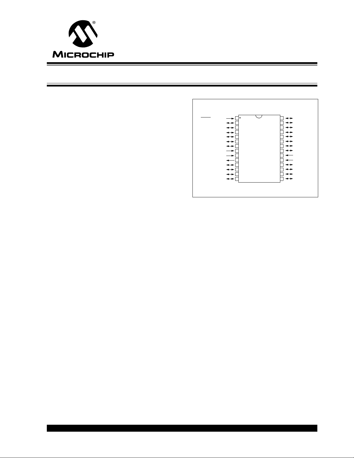
Pin Diagram
DIP, SOIC, SSOP
PIC16F872
28
27
26
25
24
23
22
21
20
19
18
17
16
15
RB7/PGD
RB6/PGC
RB5
RB4
RB3/PGM
RB2
RB1
RB0/INT
V
DD
V
SS
RC7
RC6
RC5/SDO
RC4/SD I/SDA
MCLR/VPP/TH V
RA0/AN0
RA1/AN1
RA2/AN2/V
RA3/AN3/V
OSC2/CLKOUT
RC0/T1OS O/T1CKI
REF
REF
RA4/T0CKI
RA5/AN4/SS
V
OSC1/C L KIN
RC1/T1OSI
RC2/CCP1
RC3/SCK/SCL
1
2
3
4
-
+
SS
5
6
7
8
9
10
11
12
13
14
Peripheral Features:
• Timer0: 8-bit timer/counter with 8-bit prescaler
• Timer1: 16-bit timer/counter with prescaler,
can be incremented during sleep via external
crystal/clock
• Timer2: 8-bit timer/counter with 8-bit period
register, prescaler and postscaler
• One Capture, Compare, PWM module
- Capture is 16-bit, max. resolution is 12.5 ns
- Compare is 16-bit, max. resolution is 200 ns
- PWM max. resolution is 10-bit
• 10-bit multi-channel Analog-to-Digital converter
• Synchronous Serial Port (SSP) with SPI
Mode) and I
2C
(Master/Slave)
• Brown-out detection circuitry for Brown-out Reset
(BOR)
(Master
1999 Microchip Technology Inc.
Preliminary DS30221A-page 1
Page 2

PIC16F872
Key Features
PICmicro™ Mid-Range Reference Manual
(DS33023)
Operating Frequency DC - 20 MHz
Resets (and Delays) POR, BOR
FLASH Program Memory
(14-bit words)
Data Memory (bytes) 128
EEPROM Data Memory 64
Interrupts 10
I/O Ports Ports A,B,C
Timers 3
Capture/Compare/PWM module 1
Serial Communications MSSP
10-bit Analog-to-Digital Module 5 input channels
Instruction Set 35 Instructions
PIC16F872
(PWRT, OST)
2K
DS30221A-page 2 Preliminary
1999 Microchip Technology Inc.
Page 3

PIC16F872
Table of Contents
1.0 Device Overview........................................................................................................................................................................... 5
2.0 Memory Organization.................................................................................................................................................................... 7
3.0 I/O Ports................. ................................... .................................... ............................................................. ............. ............ ........ 23
4.0 Data EEPROM and FLASH Program Memory .......................................................................................................................... 29
5.0 Timer0 Module. ........................................................................................................................................................................... 37
6.0 Timer1 Module. ........................................................................................................................................................................... 41
7.0 Timer2 Module. .......................................................................................................................................................................... 45
8.0 Capture/Compare/PWM (CCP) Module(s).................................................................................................................................. 47
9.0 Master Synchronous Serial Port (MSSP) Module........................................................ ............................................................... 53
10.0 Analog-to-Digital Converter (A/D) Module ..................................................................................................................................85
11.0 Special Features of the CPU......................................................................................................................................................95
12.0 Instruction Set Summary........................................................................................................................................................... 111
13.0 Development Support............................................................................................................................................................... 119
14.0 Electrical Characteristics........................................................................................................................................................... 125
15.0 DC and AC Characteristics Graphs and Tables .......................................................................................................................143
16.0 Packaging Infor mation...................... ............. ................................... ............. ........................................................... ............ .... 145
Appendix A: Revision History......................................................................................................................................................... 149
Appendix B: Conversion Considerations................................................................................ .... .. .... .............................................. 149
Index ......................................... .. .. .. .. .. .. ....... .. .. .. .. .. .. .. ..... .. .. .. .. .... .. .. ..... .. .. .. .. .. .. .. .. ...............................................................151
On-Line Support................................................................................................................................................................................. 157
Product Identification System............................................................................................................................................................ 159
To Our Valued Customers
Most Current Data Sheet
To obtain the most up-to-date version of this data sheet, please register at our Worldwide Web site at:
http://www.microchip.com
You can determine the version of a data sheet by examining its literature number found on the bottom outside corner of any page.
The last character of the literature number is the version number. e.g., DS30000A is version A of document DS30000.
New Customer Notification System
Register on our web site (www.microchip.com/cn) to receive the most current information on our products.
Errata
An errata sheet may exist for current devices, describing minor operational differences (from the data sheet) and recommended
workarounds. As device/documentation issues become known to us, w e will pub lish an errata sheet. The errata will specify the re vision of silicon and revision of document to which it applies.
To determine if an errata sheet exists for a particular device, please check with one of the following:
• Microchip’s Worldwide Web site; http://www.microchip.com
• Your local Microchip sales office (see last page)
• The Microchip Corporate Literature Center; U.S. FAX: (480) 786-7277
When contacting a sales office or the literature center, please specify which device, revision of silicon and data sheet (include liter-
ature number) you are using.
Corrections to this Data Sheet
We constantly strive to improve the quality of all our products and documentation. W e hav e spent a great deal of time to ensure that
this document is correct. However, we realize that we may have missed a few things. If you find any information that is missing or
appears in error, please:
• Fill out and mail in the reader response form in the back of this data sheet.
• E-mail us at webmaster@microchip.com.
We appreciate your assistance in making this a better document.
1999 Microchip Technology Inc.
Preliminary DS30221A-page 3
Page 4

PIC16F872
NOTES:
DS30221A-page 4 Preliminary
1999 Microchip Technology Inc.
Page 5

PIC16F872
1.0 DEVICE OVERVIEW
This document contains device-specific information.
Additional information may be found in the PICmicro™
Mid-Range Reference Manual, (DS33023), which may
be obtained from your local Microchip Sales Representative or downloaded from the Microchip website. The
Reference Manual should be considered a comple-
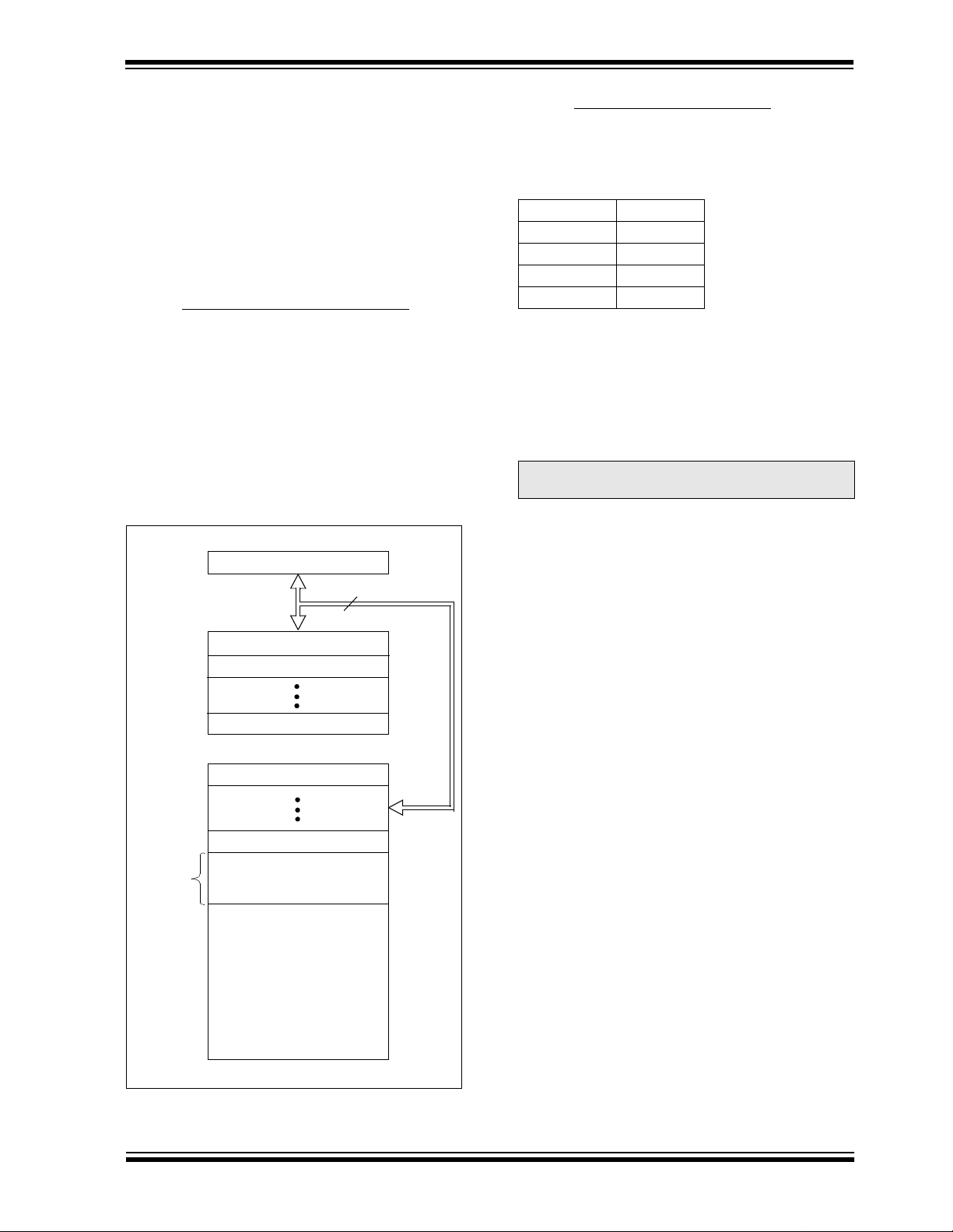
FIGURE 1-1: PIC16F872 BLOCK DIAGRAM
Device Program
FLASH
PIC16F872 2K 128 Bytes 64 Bytes
FLASH
Program
Memory
Program
OSC1/CLKIN
OSC2/CLKOUT
Bus
14
Instruction reg
Instruction
Decode &
Control
Timing
Generation
Data Memory Data
EEPROM
13
Program Counter
8 Level Stack
(13-bit)
RAM Addr (1)
Direct Addr
8
Start-up Timer
Power-up
Timer
Oscillator
Power-on
Reset
Watchdog
Timer
Brown-out
Reset
In-Circuit
Debugger
Low-Voltage
Programming
7
mentary document to this data she et, and is high ly recommended reading for a better understanding of the
device architecture and operation of the peripheral
modules.
This data sheet covers the PIC16F872 device. The
PIC16F872 is a 28-pin device and its block diagram is
shown in Figure 1-1.
3
8
Data Bus
RAM
File
Registers
Addr MUX
FSR reg
STATUS reg
ALU
W reg
9
8
MUX
8
Indirect
Addr
PORTA
PORTB
PORTC
RA0/AN0
RA1/AN1
RA2/AN2/VREFRA3/AN3/VREF+
RA4/T0CKI
RA5/AN4/SS
RB0/INT
RB1
RB2
RB3/PGM
RB4
RB5
RB6/PGC
RB7/PGD
RC0/T1OSO/T1CKI
RC1/T1OSI
RC2/CCP1
RC3/SCK/SCL
RC4/SDI/SDA
RC5/SDO
RC6
RC7
VDD, VSS
MCLR
Data EEPROM
CCP1
Synchronous
Serial Port
Note 1: Higher order bits are from the STATUS register.
1999 Microchip Technology Inc.
10-bit A/DTimer0 Timer1 Timer2
Preliminary DS30221A-page 5
Page 6

PIC16F872
TABLE 1-1: PIC16F872 PINOUT DESCRIPTION
Pin Name
OSC1/CLKIN 9 9 I
OSC2/CLKOUT 10 10 O — Oscillator crystal output. Connects to crystal or resonator in crystal
/VPP/THV 1 1 I/P ST Master clear (reset) input or programming voltage input or high
MCLR
RA0/AN0 2 2 I/O TTL RA 0 c a n al so be analog inpu t0.
RA1/AN1 3 3 I/O TTL RA 1 c a n al so be analog inpu t1.
RA2/AN2/V
RA3/AN3/V
RA4/T0CKI 6 6 I/O ST RA4 can also be the cloc k inp ut to the Timer0 module . Outp ut
RA5/SS/
RB0/INT 21 21 I/O
RB1 22 22 I/O TTL
RB2 23 23 I/O TTL
RB3/PGM 24 24 I/O
RB4 25 2 5 I/O TTL Interrupt on cha n g e pi n .
RB5 26 2 6 I/O TTL Interrupt on cha n g e pi n .
RB6/PGC 27 27 I/O
RB7/PGD 28 28 I/O
RC0/T1OSO /T 1 C K I 11 11 I/O ST RC0 can also be the Timer1 oscillator output or Timer1 cl ock
RC1/T1OSI 12 12 I/O ST RC1 can also be the Timer1 oscillator input.
RC2/CCP1 13 13 I/O ST RC2 can also be the Capture1 input/Compare1 outpu t/PWM1
RC3/SCK/SCL 14 14 I/O ST RC3 can also be the synchronous serial clo ck input /output for
RC4/SDI/SDA 15 15 I/O ST RC4 can also be the SPI Data In (SPI mode) or
RC5/SDO 16 16 I/O ST RC5 can also be the SPI Data Out (SPI mode).
RC6 17 17 I/O ST
RC7 18 18 I/O ST
SS 8, 19 8, 19 P — Ground reference for logic and I/O pins.
V
DD 20 20 P — Positive supply for logic and I/O pins.
V
Legend: I = input O = output I/O = input/output P = power
Note 1: This buffer is a Schmitt Trigger input when configured as the external interrupt or LVP.
REF- 4 4 I/O TTL RA2 can also be analog input2 or negative analog reference
REF+ 5 5 I/O TTL RA3 can also be analog input3 or positive analog reference
AN4 7 7 I/O TTL RA 5 c a n al so be analog in pu t 4 or t h e s lave sel ect for the
2: This buffer is a Schmitt Trigger input when used in serial programming mode.
3: This buffer is a Schmitt Trigger input when configured in RC oscillator mode and a CMOS input otherwise.
DIP
Pin#
— = Not used TTL = TTL input ST = Schmitt Trigger input
SOIC
Pin#
I/O/P
Type
Buffer
Type
ST/CMOS
TTL/ST
TTL/ST
TTL/ST
TTL/ST
Description
(3)
Oscillator crystal input/external clock source input.
oscillator mode. In RC mode, the OSC2 pin outputs CLKOUT,
which has 1/4 the frequency of OSC1 and denotes the instruction
cycle rate.
voltage test mode control. This pin is an active low reset to the
device.
PORTA is a bi-directional I/O port.
voltage.
voltage.
is open drain type.
synchronous serial port.
PORTB is a bi-directi onal I/O port. PORTB can be sof tware
programmed f or internal weak pull-up on all inputs.
(1)
(1)
(2)
(2)
RB0 can also be the external int er rupt pin.
RB3 can als o be the low voltage pro gra m m i ng input.
Interrupt on change pin or In-Circuit Debugger pin. Serial
programming clock.
Interrupt on change pin or In-Circuit Debugger pin. Serial
programming data.
PORTC is a bi-directional I/O port.
input.
output.
2
both SPI and I
data I/O (I
C modes.
2
C mode).
DS30221A-page 6 Preliminary
1999 Microchip Technology Inc.
Page 7
PIC16F872
2.0 MEMORY ORGANIZATION
There are three memory blocks in each of these
PICmicro
Memory have separate buses, so that concurrent
access can occur, and is detailed in this section. The
EEPROM data memory block is detailed in
Section 4.0.
Additional inf ormation on de vice m emory may be f ound
in the PICmicro Mid-Range Reference Manual,
(DS33023).
2.1 Program Memory Organization
The PIC16F872 dev ices ha v e a 13-b it prog ram co unter
capable of addressing an 8K x 14 program memory
space. The PIC16F872 device has 2K x 14 words of
FLASH program me mory. Accessing a locati on above
the physically implemented address will cause a wraparound.
The reset vector is at 0000h and the interrupt vector is
at 0004h.
FIGURE 2-1: PIC16F872 PROGRAM
®
MCUs. The Program Memory and Data
MEMORY MAP AND STACK
PC<12:0>
CALL, RETURN
RETFIE, RETLW
13
2.2 Data Memory Organization
The data memory is partitioned into multiple banks
which contain the General Purpose Registers and the
Special Function Registers. Bits RP1(STATUS<6>)
and RP0 (STATUS<5>) are the bank select bits.
RP<1:0> Bank
00 0
01 1
10 2
11 3
Each bank extends up to 7Fh (128 bytes). The lower
locations of each bank are reserved for the Special
Function Registers . Abo v e the Spec ial Fun ction Re gisters are General Purpose Registers, implemented as
static RAM. All implemented banks contain Special
Function Registers. Some “high use” Special Function
Registers from one bank may be mirrored in another
bank for code reduction and quicker access.
Note: EEPROM Data Memory description can b e
found in Section 4.0 of this Data Sheet
2.2.1 GENERAL PURPOSE REGISTER FILE The register file can be a ccessed ei ther direc tly, or indi-
rectly through the File Select Register FSR.
On-Chip
Program
Memory
Stack Level 1
Stack Level 2
Stack Level 8
Reset Vector
Interrupt Vector
Page 0
0000h
0004h
0005h
07FFh
0800h
1FFFh
1999 Microchip Technology Inc.
Preliminary DS30221A-page 7
Page 8
PIC16F872
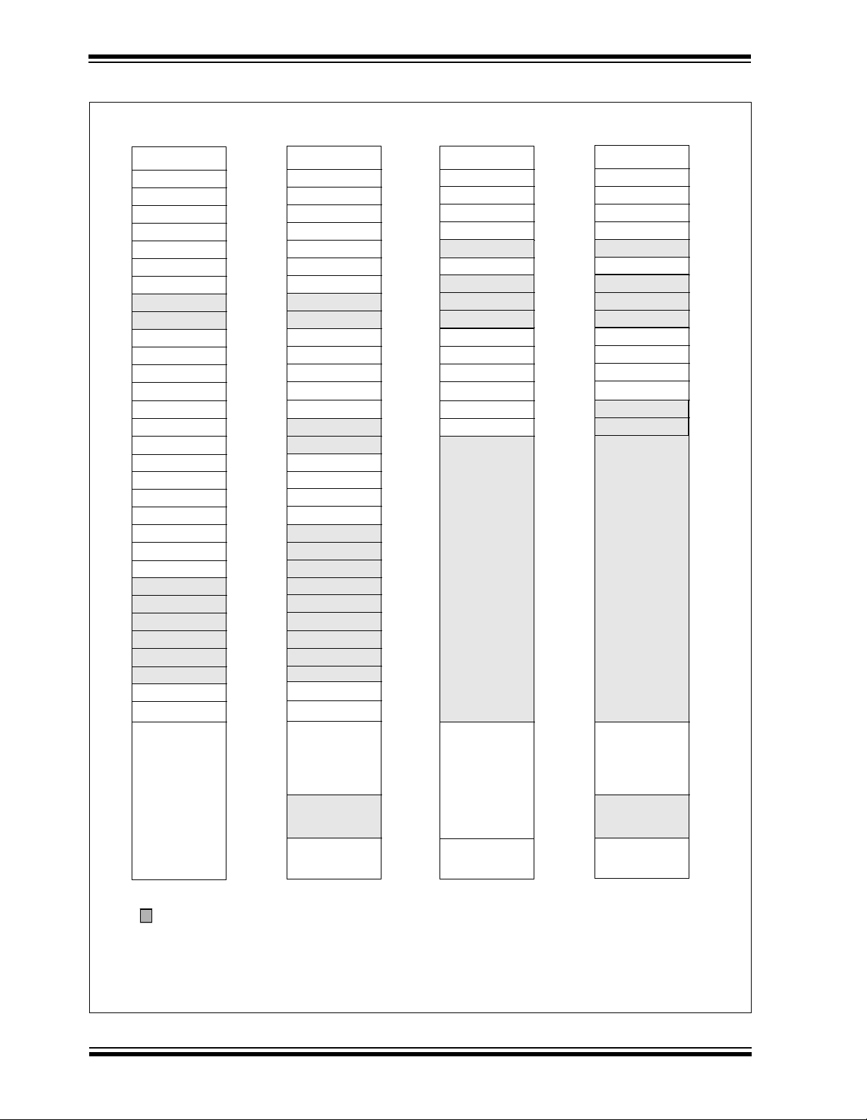
FIGURE 2-2: PIC16F872 REGISTER FILE MAP
PCL
FSR
PR2
(*)
80h
81h
82h
83h
84h
85h
86h
87h
88h
89h
8Ah
8Bh
8Ch
8Dh
8Eh
8Fh
90h
91h
92h
93h
94h
95h
96h
97h
98h
99h
9Ah
9Bh
9Ch
9Dh
9Eh
9Fh
A0h
BFh
C0h
EFh
F0h
FFh
Indirect addr.
TMR0
PCL
STATUS
FSR
PORTA
PORTB
PORTC
(*)
00h
01h
02h
03h
04h
05h
06h
07h
Indirect addr .
OPTION_REG
STATUS
08h
09h
PCLATH
INTCON
PIR1
PIR2
TMR1L
TMR1H
T1CON
TMR2
T2CON
SSPBUF
SSPCON
CCPR1L
CCPR1H
CCP1CON
0Ah
0Bh
0Ch
0Dh
0Eh
0Fh
10h
11h
12h
13h
14h
15h
16h
17h
PCLATH
INTCON
SSPCON2
SSPADD
SSPSTAT
18h
19h
1Ah
1Bh
1Ch
1Dh
ADRESH
ADCON0 ADCON1
1Eh
1Fh
20h
ADRESL
General
Purpose
Register
General
Purpose
32 Bytes
Register
96 Bytes
accesses
Bank 0
7Fh
70h-7Fh
Bank 1
TRISA
TRISB
TRISC
PIE1
PIE2
PCON
Indirect addr.
TMR0
PCL
STATUS
FSR
PORTB
PCLATH
INTCON
EEDATA
EEADR
EEDATH
EEADRH
accesses
20h-7Fh
accesses
70h-7Fh
Bank 2
File
Address
(*)
100h
101h
102h
103h
104h
Indirect addr.
OPTION_REG
PCL
STATUS
FSR
105h
106h
TRISB
107h
108h
109h
10Ah
10Bh
10Ch
10Dh
10Eh
10Fh
PCLATH
INTCON
EECON1
EECON2
Reserved
Reserved
110h
120h
(*)
180h
181h
182h
183h
184h
185h
186h
187h
188h
189h
18Ah
18Bh
18Ch
18Dh
(1)
18Eh
(1)
18Fh
190h
1A0h
accesses
A0h - BFh
1BFh
1C0h
16Fh
170h
17Fh
accesses
70h-7Fh
1EFh
1F0h
1FFh
Bank 3
Unimplemented data memory locations, read as ’0’.
* Not a physical register.
Note 1: These registers are reserved; maintain these registers clear.
DS30221A-page 8 Preliminary
1999 Microchip Technology Inc.
Page 9
PIC16F872
2.2.2 SPECIAL FUNCTION REGISTERS
The Special Function Registers can be classified into
two sets: core (CPU) and peripheral. Those registers
The Special Function Registers are registers used by
the CPU and peripheral modules for controlling the
desired operation of the device. These registers are
implemented as static RAM. A list of these registers is
given in Table 2-1.
associated with the core functions are described in
detail in this section. Those related to the operation of
the peripheral features are described in detail in the
peripheral feature section.
TABLE 2-1: SPECIAL FUNCTION REGISTER SUMMARY
Value on:
Address Name Bit 7 Bit 6 Bit 5 Bit 4 Bit 3 Bit 2 Bit 1 Bit 0
POR,
BOR
Bank 0
(3)
00h
01h TMR0 Timer0 module’s register xxxx xxxx uuuu uuuu
02h
03h
04h
05h POR TA
06h POR TB PORTB Data Latch when written: PORTB pins when read xxxx xxxx uuuu uuuu
07h PORTC PORTC Data Latch when written: PORTC pins when read xxxx xxxx uuuu uuuu
08h — Unimplemented — —
09h
0Ah
0Bh
0Ch PIR1 (4) ADIF (4) (4) SSPIF CCP1IF TMR2IF TMR1IF r0rr 0000 r0rr 0000
0Dh PIR2
0Eh TMR1L Holding register for the Least Significant Byte of the 16-bit TMR1 register xxxx xxxx uuuu uuuu
0Fh TMR1H Holding register for the Most Significant Byte of the 16-bit TMR1 register xxxx xxxx uuuu uuuu
10h T1CON
11h TMR2 Timer2 module’s register 0000 0000 0000 0000
12h T2CON
13h SSPBUF Synchronous Serial Port Receive Buffer/Transmit Register xxxx xxxx uuuu uuuu
14h SSPCON WCOL SSPOV SSPEN CKP SSPM3 SSPM2 SSPM1 SSPM0 0000 0000 0000 0000
15h CCPR1L Capture/Compare/PWM Register1 (LSB) xxxx xxxx uuuu uuuu
16h CCPR1H Capture/Compare/PWM Register1 (MSB) xxxx xxxx uuuu uuuu
17h CCP1CON
18h — Unimplemented — —
19h — Unimplemented — —
1Ah — Unimplemented — —
1Bh — Unimplemented — —
1Ch — Unimplemented — —
1Dh — Unimplemented — —
1Eh ADRESH A/D Result Register High Byte xxxx xxxx uuuu uuuu
1Fh ADCON0 ADCS1 ADCS0 CHS2 CHS1 CHS0
Legend: x = unknown, u = unchanged, q = value depends on condition, - = unimplemented read as ’0’, r = reserved.
Note 1: The upper byte of the program counter is not directly accessible. PCLA TH is a holding register for the PC<12:8> whose
INDF Addressing this location uses contents of FSR to address data memory (not a physical register) 0000 0000 0000 0000
(3)
PCL Program Counter's (PC) Least Significant Byte 0000 0000 0000 0000
(3)
STATUS IRP RP1 RP0 TO PD ZDCC0001 1xxx 000q quuu
(3)
FSR Indirect data memory address pointer xxxx xxxx uuuu uuuu
— — PORTA Data Latch when written: PORTA pins when read --0x 0000 --0u 0000
— Unimpleme nted — —
(1,3)
PCLATH — — — Write Buffer for the upper 5 bits of the Program Counter ---0 0000 ---0 0000
(3)
INTCON GIE PEIE T0IE INTE RBIE T0IF INTF RBIF 0000 000x 0000 000u
— (4) — EEIF BCLIF — — (4) -r-0 0--r -r-0 0--r
— — T1CKPS1 T1CKPS0 T1OSCEN T1SYNC TMR1CS TMR1ON --00 0000 --uu uuuu
— TOUTPS3 TOUTPS2 TOUTPS1 TOUTPS0 TMR2ON T2CKPS1 T2CKPS0 -000 0000 -000 0000
— — CCP1X CCP1Y CCP1M3 CCP1M2 CCP1M1 CCP1M0 --00 0000 --00 0000
GO/
DONE
—ADON0000 00-0 0000 00-0
Shaded locations are unimplemented, read as ‘0’.
contents are transferred to the upper byte of the program counter.
2: Other (non power-up) resets include external reset through MCLR
and Watchdog Timer Reset.
3: These registers can be addressed from any bank.
4: These bits are reserved; always maintain these bits clear.
Value on
all other
resets
(2)
1999 Microchip Technology Inc.
Preliminary DS30221A-page 9
Page 10
PIC16F872
TABLE 2-1: SPECIAL FUNCTION REGISTER SUMMARY (CONTINUED)
Address Name Bit 7 Bit 6 Bit 5 Bit 4 Bit 3 Bit 2 Bit 1 Bit 0
POR,
BOR
Value on:
Bank 1
(3)
80h
81h OPTION_REG RBPU
82h
83h
84h
85h TRISA
86h TRISB PORTB Data Direction Register 1111 1111 1111 1111
87h TRISC PORTC Data Direction Register 1111 1111 1111 1111
88h — Unimplemented — —
89h — Unimplemented — —
8Ah
8Bh
8Ch PIE1 (4) ADIE (4) (4) SSPIE CCP1IE TMR2IE TMR1IE r0rr 0000 r0rr 0000
8Dh PIE2
8Eh PCON
8Fh — Unimplemented — —
90h — Unimplemented — —
91h SSPCON2 GCEN ACKSTAT ACKDT ACKEN RCEN PEN RSEN SEN 0000 0000 0000 0000
92h PR2 Timer2 Period Register 1111 1111 1111 1111
93h SSPADD
94h SSPSTAT SMP CKE D/A
95h — Unimplemented — —
96h — Unimplemented — —
97h — Unimplemented — —
98h — Unimplemented — —
99h — Unimplemented — —
9Ah — Unimplemented — —
9Bh — Unimplemented — —
9Ch — Unimplemented — —
9Dh — Unimplemented — —
9Eh ADRESL A/D Result Register Low Byte xxxx xxxx uuuu uuuu
9Fh ADCON1 ADFM
INDF Addressing this location uses contents of FSR to address data memory (not a physical register) 0000 0000 0000 0000
INTEDG T0CS T0SE PSA PS2 PS1 PS0 1111 1111 1111 1111
(3)
PCL Program Counter’s (PC) Least Significant Byte 0000 0000 0000 0000
(3)
STATUS IRP RP1 RP0 TO PD ZDCC0001 1xxx 000q quuu
(3)
FSR Indirect data memory address pointer xxxx xxxx uuuu uuuu
— — PORTA Data Direction Register --11 1111 --11 1111
(1,3)
PCLATH — — — Write Buffer for the upper 5 bits of the Program Counter ---0 0000 ---0 0000
(3)
INTCON GIE PEIE T0IE INTE RBIE T0IF INTF RBIF 0000 000x 0000 000u
— (4) — EEIE BCLIE — — (4) -r-0 0--r -r-0 0--r
— — — — — —PORBOR ---- --qq ---- --uu
Synchronous Serial Port (I
— — — PCFG3 PCFG2 PCFG1 PCFG0 0--- 0000 0--- 0000
2
C mode) Address Register
PSR/WUA BF 0000 0000 0000 0000
0000 0000 0000 0000
Legend: x = unknown, u = unchanged, q = value depends on condition, - = unimplemented read as ’0’, r = reserved.
Shaded locations are unimplemented, read as ‘0’.
Note 1: The upper byte of the program counter is not directly accessible. PCLATH is a holding register for the PC<12:8> whose
contents are transferred to the upper byte of the program counter.
2: Other (non power-up) resets include external reset through MCLR
and Watchdog Timer Reset.
3: These registers can be addressed from any bank.
4: These bits are reserved; always maintain these bits clear.
Value on
all other
resets
(2)
DS30221A-page 10 Preliminary
1999 Microchip Technology Inc.
Page 11
PIC16F872
TABLE 2-1: SPECIAL FUNCTION REGISTER SUMMARY (CONTINUED)
Value on:
Address Name Bit 7 Bit 6 Bit 5 Bit 4 Bit 3 Bit 2 Bit 1 Bit 0
POR,
BOR
Bank 2
(3)
100h
101h TMR0 Timer0 module’s register xxxx xxxx uuuu uuuu
102h
103h
104h
105h — Unimplemented — —
106h PORTB PORTB Data Latch when written: PORTB pins when read xxxx xxxx uuuu uuuu
107h — Unimplemented — —
108h — Unimplemented — —
109h — Unimplemented — —
10Ah
10Bh
10Ch EEDATA EEPROM data register xxxx xxxx uuuu uuuu
10Dh EEADR EEPROM address register xxxx xxxx uuuu uuuu
10Eh EEDATH
10Fh EEADRH
INDF Addressing this location uses contents of FSR to address data memory (not a physical register) 0000 0000 0000 0000
(3)
PCL Program Counter's (PC) Least Significant Byte 0000 0000 0000 0000
(3)
STAT US IRP RP1 RP0 TO PD Z DC C 0001 1xxx 000q quuu
(3)
FSR Indirect data memory address pointer xxxx xxxx uuuu uuuu
(1,3)
PCLATH — — — Write Buffer for the upper 5 bits of the Program Counter ---0 0000 ---0 0000
(3)
INTCON GIE PEIE T0IE INTE RBIE T0IF INTF RBIF 0000 000x 0000 000u
— — EEPROM data register high byte xxxx xxxx uuuu uuuu
— — — EEPROM address register high byte xxxx xxxx uuuu uuuu
Bank 3
(3)
180h
181h OPTION_REG RBPU
182h
183h
184h
185h — Unimplemented — —
186h TRISB PORTB Data Direction Register 1111 1111 1111 1111
187h — Unimplemented — —
188h — Unimplemented — —
189h — Unimplemented — —
18Ah
18Bh
18Ch EECON1 EEPGD
18Dh EECON2 EEPROM control register2 (not a physical register) ---- ---- ---- ---18Eh — Reserved maintain clear 0000 0000 0000 0000
18Fh — Reserved maintain clear 0000 0000 0000 0000
Legend: x = unknown, u = unchanged, q = value depends on condition, - = unimplemented read as ’0’, r = reserved.
Note 1: The upper byte of the program counter is not directly accessible. PCLA TH is a holding register for the PC<12:8> whose
INDF Addressing this location uses contents of FSR to address data memory (not a physical register) 0000 0000 0000 0000
INTEDG T0CS T0SE PSA PS2 PS1 PS0 1111 1111 1111 1111
(3)
PCL Program Counter's (PC) Least Significant Byte 0000 0000 0000 0000
(3)
STAT US IRP RP1 RP0 TO PD Z DC C 0001 1xxx 000q quuu
(3)
FSR Indirect data memory address pointer xxxx xxxx uuuu uuuu
(1,3)
PCLATH — — —
(3)
INTCON GIE PEIE T0IE INTE RBIE T0IF INTF RBIF 0000 000x 0000 000u
— — — WRERR WREN WR RD x--- x000 x--- u000
Write Buffer for the upper 5 bits of the Program Counter
---0 0000 ---0 0000
Shaded locations are unimplemented, read as ‘0’.
contents are transferred to the upper byte of the program counter.
2: Other (non power-up) resets include external reset through MCLR
and Watchdog Timer Reset.
3: These registers can be addressed from any bank.
4: These bits are reserved; always maintain these bits clear.
Value on
all other
resets
(2)
1999 Microchip Technology Inc.
Preliminary DS30221A-page 11
Page 12

PIC16F872
2.2.2.1 STATUS REGISTER
The STATUS register contains the arithmetic status of
the ALU, the R ESET st atus an d the ba nk sel ect bi ts f or
data memory.
The STATUS register can be the destination for any
instruction, as with any other register. If the STATUS
register is the destination for an instruction that affects
the Z, DC or C bits, then the write to these three bits is
disabled. The se bi ts ar e set or c leared accordi ng to the
device logic. Fur th er more, the TO
writable, therefore, the result of an instruction with the
STATUS re gister as desti nation may be different t han
intended.
and PD bits are not
For example, CLRF STATUS will clear the up p er- t h ree
bits and set th e Z bi t. T his l ea v es the STATUS register
as 000u u1uu (where u = unchanged).
It is recommended, therefore, that only BCF, BSF,
SWAPF and MOVWF instructions are used to alter the
STATUS register, because these instructions do not
affect the Z, C or DC b its from the STA TUS register. For
other instructions not affecting any status bits, see the
"Instruction Set Summary."
Note: The C and DC bits operate as a borrow
and digit borrow bit, respectively, in subtraction. See the SUBLW and SUBWF
instructions for examples.
REGISTER 2-1: STATUS REGISTER (ADDRESS 03h, 83h, 103h, 183h)
R/W-0 R/W-0 R/W-0 R-1 R-1 R/W-x R/W-x R/W-x
IRP RP1 RP0 TO PD Z DC C R = Readable bit
bit7 bit0
bit 7: IRP: Register Bank Select bit (used for indirect address in g)
1 = Bank 2, 3 (100h - 1FFh)
0 = Bank 0, 1 (00h - FFh)
bit 6-5: RP<1:0>: Register Bank Select bits (used for direct addressing)
11 = Bank 3 (180h - 1FFh)
10 = Bank 2 (100h - 17Fh)
01 = Bank 1 (80h - FFh)
00 = Bank 0 (00h - 7Fh)
Each bank is 128 bytes
bit 4: TO
bit 3: PD
bit 2: Z: Zero bit
bit 1: DC: Digit carry/borrow
bit 0: C: Carry/borrow
: Time-out bit
1 = After power-up, CLRWDT instruction, or SLEEP in struction
0 = A WDT time-out occurred
: Power-down bit
1 = After power-up or by the CLRWDT instruction
0 = By execution of the SLEEP instruction
1 = The result of an arithmetic or logic operation is zero
0 = The result of an arithmetic or logic operation is not zero
bit (ADDWF, ADDLW,SUBLW,SUBWF instructions)
(for borrow
1 = A carry-out from the 4th low order bit of the result occurred
0 = No carry-out from the 4th low order bit of the result
1 = A carry-out from the most significant bit of the result occurred
0 = No carry-out from the most significant bit of the result occurred
Note: For borrow
the second operand. For rotate (RR F, RLF) instructions, this bit is loaded with ei ther the high or low o rder
bit of the source register.
the polarity is reversed)
bit (ADDWF, ADDLW,SUBLW,SUBWF instructions)
the polarity is reversed. A subtraction is executed by adding the two’s complement of
W = Writable bit
U = Unimplemented bit,
read as ‘0’
- n= Value at POR reset
DS30221A-page 12 Preliminary
1999 Microchip Technology Inc.
Page 13

PIC16F872
2.2.2.2 OPTION_REG REGISTER
The OPTION_REG Regis ter is a read ab le and writab le
register , which contai ns various c ontrol bits to c onfigure
the TMR0 prescaler/WDT postscaler (single assignable regist er kno wn also as the prescale r), the Ext ernal
INT Interrupt, TMR0 and the w eak pul l-ups on PO R TB .
REGISTER 2-2: OPTION_REG REGISTER (ADDRESS 81h, 181h)
R/W-1 R/W-1 R/W-1 R/W-1 R/W-1 R/W-1 R/W-1 R/W-1
RBPU INTEDG T0CS T0SE PSA PS2 PS1 PS0 R = Readable bit
bit7 bit0
bit 7: RBPU: PORTB Pull-up Enable bit
1 = PORTB pull-ups are disabled
0 = PORTB pull-ups are enabled by individual port latch values
bit 6: INTEDG: Interrupt Edge Select bit
1 = Interrupt on rising edge of RB0/INT pin
0 = Interrupt on falling edge of RB0/INT pin
bit 5: T0CS: TMR0 Clock Source Select bit
1 = Transition on RA4/T0CKI pin
0 = Internal instruction cycle clock (CLKOUT)
bit 4: T0SE: TMR0 Source Edge Select bit
1 = Increment on high-to-low transition on RA4/T0CKI pin
0 = Increment on low-to-high transition on RA4/T0CKI pin
bit 3: PSA: Prescaler Assignment bit
1 = Prescaler is assigned to the WDT
0 = Prescaler is assigned to the Timer0 module
bit 2-0: PS<2:0>: Prescaler Rate Select bits
Bit Value T MR0 Rate WDT Rate
000
001
010
011
100
101
110
111
1 : 2
1 : 4
1 : 8
1 : 16
1 : 32
1 : 64
1 : 128
1 : 256
1 : 1
1 : 2
1 : 4
1 : 8
1 : 16
1 : 32
1 : 64
1 : 128
Note: To achieve a 1:1 prescaler assignme nt for
the TMR0 register, assign the prescaler to
the Watchdog Timer.
W = Writable bit
U = Unimplemented bit,
read as ‘0’
- n= Value at POR reset
Note: When using Low Voltage ICSP Programming (LVP) and the pull-ups on PORTB are enabled, bit 3 in the
TRISB register must be c leared to disable the pull-up on RB3 and ens ure the proper operat ion of the dev ice.
1999 Microchip Technology Inc.
Preliminary DS30221A-page 13
Page 14

PIC16F872
2.2.2.3 INTCON REGISTER
The INTCON Regi ster i s a rea dab le a nd w ritabl e regi s-
ter, which contains various enable and flag bits for the
TMR0 register overflow, RB Port change and External
RB0/INT pin interrupts.
Note: Interrupt flag bits get set when an in terrupt
condition occurs , regardless of the sta te of
its corresponding enable bit or the global
enable bit, GIE (INTCON<7>). User software should ensure the appropriate interrupt flag bits are clear prior to enabling an
interrupt.
REGISTER 2-3: INTCON REGISTER (ADDRESS 0Bh, 8Bh, 10Bh, 18Bh)
R/W-0 R/W-0 R/W-0 R/W-0 R/W-0 R/W-0 R/W-0 R/W-x
GIE PEIE T0IE INTE RBIE T0IF INTF RBIF R = Readable bit
bit7 bit0
bit 7: GIE: Global Interrupt Enable bit
1 = Enables all un-masked interrupts
0 = Disables all interrupts
bit 6: PEIE: Peripheral Interrupt Enable bit
1 = Enables all un-masked peripheral interrupts
0 = Disables all peripheral interrupts
bit 5: T0IE: TMR0 Overflow Interrupt Enable bit
1 = Enables the TMR0 interrupt
0 = Disables the TMR0 interrupt
bit 4: INTE: RB0/INT External Interrupt Enable bit
1 = Enables the RB0/INT external interrupt
0 = Disables the RB0/INT external interrupt
bit 3: RBIE: RB Port Change Interrupt Enable bit
1 = Enables the RB port change interrupt
0 = Disables the RB port change interrupt
bit 2: T0IF: TMR0 Overflow Interrupt Flag bit
1 = TMR0 register has overflowed (must be cleared in software)
0 = TMR0 register did not overflow
bit 1: INTF: RB0/INT External Interrupt Flag bit
1 = The RB0/INT external interrupt occurred (must be cleared in software)
0 = The RB0/INT external interrupt did not occur
bit 0: RBIF: RB Port Change Interrupt Flag bit
1 = At least one of the RB<7:4> pins changed state (must be cleared in software)
0 = None of the RB<7:4> pins have changed state
W = Writab le bit
U = Unimplemented bit,
read as ‘0’
- n= Value at POR reset
DS30221A-page 14 Preliminary
1999 Microchip Technology Inc.
Page 15

2.2.2.4 PIE1 REGISTER
PIC16F872
The PIE1 register contain s the individual en able bits for
the peri pheral interrupts.
Note: Bit PEIE (INTCON<6>) must be set to
enable any peripheral interrupt.
REGISTER 2-4: PIE1 REGISTER (ADDRESS 8Ch)
R/W-0 R/W-0 R/W-0 R/W-0 R/W-0 R/W-0 R/W-0 R/W-0
— ADIE — — SSPIE CCP1IE TMR2IE TMR1IE R = Readable bit
bit7 bit0
bit 7: Reserved: Always maintain this bit clear
bit 6: ADIE: A/D Converter Interrupt Enable bit
1 = Enables the A/D converter interrupt
0 = Disables the A/D converter interrupt
bit 5-4: Reserved: Always maintain this bit clear
bit 3: SSPIE: Synchronous Serial Port Interrupt Enable bit
1 = Enables the SSP interrupt
0 = Disables the SSP interrupt
bit 2: CCP1IE: CCP1 Interrupt Enable bit
1 = Enables the CCP1 interrupt
0 = Disables the CCP1 interrupt
bit 1: TMR2IE: TMR2 to PR2 Match Interrupt Enable bit
1 = Enables the TMR2 to PR2 match interrupt
0 = Disables the TMR2 to PR2 match interrupt
bit 0: TMR1IE: TMR1 Overflow Interrupt Enable bit
1 = Enables the TMR1 overflow interrupt
0 = Disables the TMR1 overflow interrupt
W = Writable bit
U = Unimplemented bit,
- n= Value at POR reset
read as ‘0’
1999 Microchip Technology Inc.
Preliminary DS30221A-page 15
Page 16

PIC16F872
2.2.2.5 PIR1 REGISTER
The PIR1 register contains the individual flag bits for
the peri pheral interrupts.
Note: Interrupt flag bits get set when an in terrupt
condition occurs , regardless of the sta te of
its corresponding enable bit or the global
enable bit, GIE (INTCON<7>). User software should ensure the appropriate interrupt bits are clear prior to enabling an
interrupt.
REGISTER 2-5: PIR1 REGISTER (ADDRESS 0Ch)
R/W-0 R/W-0 R/W-0 R/W-0 R/W-0 R/W-0 R/W-0 R/W-0
— ADIF — — SSPIF CCP1IF TMR2IF TMR1IF R = Readable bit
bit7 bit0
bit 7: Reserved: Always maintain this bit clear
bit 6: ADIF: A/D Converter Interrupt Flag bit
1 = An A/D conversion completed
0 = The A/D conversion is not complete
bit 5-4: Reserved: Always maintain this bit clear
bit 3: SSPIF: Synchronous Serial Port (SSP) Interrupt Flag
1 = The SSP interrupt condition has oc curred , and mus t be cle ared in s oft w are b efore returning from the
interrupt service routine. The conditions that will set this bit are:
SPI
A transmission/reception has taken place.
2
I
C Slave
A transmission/reception has taken place.
2
C Master
I
A transmission/reception has taken place.
The initiated start condition was completed by the SSP module.
The initiated stop condition was completed by the SSP module.
The initiated restart condition was completed by the SSP module.
The initiated acknowledge condition was completed by the SSP module.
A start condition occurred while the SSP module was idle (Multimaster system).
A stop condition occurred while the SSP module was idle (Multimaster system).
0 = No SSP interrupt condition has occurred.
bit 2: CCP1IF: CCP1 Interrupt Flag bit
Capture Mode
1 = A TMR1 register capture occurred (must be cleared in software)
0 = No TMR1 register capture occurred
Compare Mode
1 = A TMR1 register compare match occurred (must be cleared in software)
0 = No TMR1 register compare match occurred
PWM Mode
Unused in this mode
bit 1: TMR2IF: TMR2 to PR2 Match Interrupt Flag bit
1 = TMR2 to PR2 match occurred (must be cleared in software)
0 = No TMR2 to PR2 match occurred
bit 0: TMR1IF: TMR1 Overflow Interrupt Flag bit
1 = TMR1 register overflowed (must be cleared in software)
0 = TMR1 regi ster did not overflow
W = Writable bit
U = Unim plemented bit,
- n= Value at POR reset
read as ‘0’
DS30221A-page 16 Preliminary
1999 Microchip Technology Inc.
Page 17

2.2.2.6 PIE2 REGISTER
The PIE2 register contain s the individual en able bits for
the SSP bus collision interrupt and the EEPROM write
operation interrupt.
REGISTER 2-6: PIE2 REGISTER (ADDRESS 8Dh)
U-0 R/W-0 U-0 R/W-0 R/W-0 U-0 U-0 R/W-0
——— EEIE BCLIE — — — R = Readable bit
bit7 bit0
bit 7: Unimplemented: Read as '0'
bit 6: Reserved: Always maintain this bit clear
bit 5: Unimplemented: Read as '0'
bit 4: EEIE: EEPROM Write Operation Interrupt Enable
1 = Enable EE Write Interrupt
0 = Disable EE Write Interrupt
bit 3: BCLIE: Bus Collision Interrupt Enable
1 = Enable Bus Collision Interrupt
0 = Disable Bus Collision Interrupt
bit 2-1: Unimplemented: Read as '0'
bit 0: Reserved: Always maintain this bit clear
W = Writable bit
U = Unimplemented bit,
- n= Value at POR reset
PIC16F872
read as ‘0’
1999 Microchip Technology Inc.
Preliminary DS30221A-page 17
Page 18

PIC16F872
2.2.2.7 PIR2 REGISTER
The PIR2 register contains the flag bits for the SSP bus
collision interrupt and the EEPROM write operation
interrupt.
.
Note: Interrupt flag bits get set when an in terrupt
condition occurs , regardless of the sta te of
its corresponding enable bit or the global
enable bit, GIE (INTCON<7>). User software should ensure the appropriate interrupt flag bits are clear prior to enabling an
interrupt.
REGISTER 2-7: PIR2 REGISTER (ADDRESS 0Dh)
U-0 R/W-0 U-0 R/W-0 R/W-0 U-0 U-0 R/W-0
——— EEIF BCLIF — — — R = Readable bit
bit7 bit0
bit 7: Unimplemented: Read as '0'
bit 6: Reserved: Always maintain this bit clear
bit 5: Unimplemented: Read as '0'
bit 4: EEIF: EEPROM Write Operation Interrupt Flag bit
1 = The write operation completed (must be cleared in software)
0 = The write operation is not complete or has not been started
bit 3: BCLIF: Bus Collision Interrupt Flag
1 = A bus collision has occurred in the SSP, when configured for I
0 = No bus collision has occurred
bit 2-1: Unimplemented: Read as '0'
bit 0: Reserved: Always maintain this bit clear
2
W = Writable bit
U = Unimplemented bit,
- n= Value at POR reset
C master mode
read as ‘0’
DS30221A-page 18 Preliminary
1999 Microchip Technology Inc.
Page 19

PIC16F872
2.2.2.8 PCON REGISTER
The Power Control (PCON) Register contains flag bits
to allow differentiation between a Power-on Reset
(POR), a Brown-o ut Re set (BOR) , a Watch-d og Re set
(WDT) and an external MCLR
Reset.
Note: BOR is unknown on POR. It must be set by
the user and checked on subsequent
resets to see if BOR is clear, indicating a
brown-out ha s occurred. The BO R status
bit is a don’t care and is not predictable if
the brown-out ci rcuit i s disabled (by clea ring the BODEN bit in the configuration
word).
REGISTER 2-8: PCON REGISTER (ADDRESS 8Eh)
U-0 U-0 U-0 U-0 U-0 U-0 R/W-0 R/W-1
— — — — — —PORBOR R = Readable bit
bit7 bit0
bit 7-2: Unimplemented: Read as '0'
bit 1: POR
bit 0: BOR
: Power-on Reset Status bit
1 = No Power-on Reset occurred
0 = A Power-on Reset occurred (must be set in software after a Power-on Reset occurs)
: Brown-out Reset Status bit
1 = No Brown-out Reset occurred
0 = A Brown-out Reset occurred (must be set in softwar e after a Brown- out Reset occurs)
W = Writable bit
U = Unimplemented bit,
- n= Value at POR reset
read as ‘0’
1999 Microchip Technology Inc.
Preliminary DS30221A-page 19
Page 20
PIC16F872
2.3 PCL and PCLATH
The program coun ter (PC) is 13-bits wide . The low b yte
comes from the PCL register, which is a readable and
writable register. The upper bits (PC<12:8>) are not
readable, but are indirectly writable through the
PCLATH register. On any reset, the upper bits of the
PC will be cleared. Figure 2-3 shows the two situations
for the loadin g of the PC . The up per e xa mple in the fi gure shows how the PC is loaded on a write to PCL
(PCLATH<4:0> → PCH). The lower example in the fig-
ure shows ho w the PC is loaded during a CALL or GOTO
instruction (PCLATH<4:3> → PCH).
FIGURE 2-3: LOADING OF PC IN
DIFFERENT SITUATIONS
PCH PCL
12 8 7 0
PC
PCLATH<4:0>
5
PCLATH
PCH PCL
12 11 10 0
PC
2
87
PCLATH<4:3>
PCLATH
11
2.3.1 COMPUTED GOTO A computed GOTO is accomplished by add ing an o ffs et
to the progra m counter (ADDWF PCL). When doing a
table read using a computed GOTO method, care
should be exercis ed i f t he table loc at ion c ros se s a PCL
memory boundary (each 256 byte block). Refer to the
application note,
“Implementing a Table Read"
(AN556).
2.3.2 STACK The PIC16CXX f amily ha s an 8-le ve l deep x 13 -bit wide
hardware stack. T he stack space is not part of either
program or data space and the stack pointer is not
readable or writab le. The PC is PUSHed onto the stac k
when a CALL instruction is executed or an interrupt
causes a branch. The stack is POPed in the event of a
RETURN,RETLW or a RETFIE instruction execution.
PCLATH is not affected by a PUSH or POP operation.
The stack oper ates as a circular b uffer . This means that
after the stack has been PUSHed e ight ti mes , th e nin th
push overw rites th e value that was stored from the firs t
push. The tenth push overwrites the second push (and
so on).
8
Instruction with
PCL as
Destination
ALU
GOTO,CALL
Opcode <10:0>
Note 1: There are no status bits to indicate stack
overflow or stack underflow conditions.
2: There are no instructions/mnemonics
called PUSH or POP. These are actions that
occur from the execution of the CALL,
RETURN, RETLW and RETFIE instructions or the vectoring to an interrupt
address.
2.4 Program Memory Paging
The PIC16CXXX architecture is capabl e of addressing
a continuous 8K word block of program memory. The
CALL and GOTO instructions provide 11 bits of the
address, which al lows br anche s within an y 2K prog ram
memory page. Therefore, the 8K words of program
memory are broken into four pages. Since the
PIC16FC872 has only 2K w ords of progr am memory or
one page, ad ditional code is not requ ired to e nsure th at
the correct page is selected before a CALL or GOTO
instruction is executed. The PCLATH<4:3> bits should
always be maintai ned as z ero s. If a return from a CALL
instruction (or interrupt) is executed, the entire 13-bit
PC is popped off the stack. Manipulation of the
PCLATH is not required for the return instructions.
2.5 Indirect Addr essing, INDF and FSR Registers
The INDF register is not a ph ysic al register . Addr essing
the INDF register will cause indirect addressing.
Indirect addressing is possible by using the INDF register. Any instruction using the INDF register actually
accesses the regist er pointed to b y the File Select Register, FSR. Reading the INDF register itself indirectly
(FSR = ’0’) will re ad 00h. Wr iting t o the INDF registe r
indirectly resu lts in a no-opera tion (although st atus bits
may be affected). An eff ec tiv e 9-bit addres s is o btaine d
by concatenatin g the 8-bit FSR register an d the IRP b it
(STATUS<7>), as shown in Figure 2-4.
A simple program to clear RAM locations 20h-2Fh
using indirect addressing is shown in Example 2-1.
EXAMPLE 2-1: INDIRECT ADDRESSING
movlw 0x20 ;initialize pointer
movwf FSR ;to RAM
NEXT clrf INDF ;clear INDF register
incf FSR,F ;inc pointer
btfss FSR,4 ;all done?
goto NEXT ;no clear next
CONTINUE
: ;yes continue
DS30221A-page 20 Preliminary
1999 Microchip Technology Inc.
Page 21

FIGURE 2-4: DIRECT/INDIRECT ADDRESSING
RP1:RP0 6
from opcode
0
PIC16F872
Indirect AddressingDirect Addressing
IRP FSR register
7
0
bank select location select
00 01 10 11
00h
Data
(1)
Memory
7Fh
Bank 0 Bank 1 Bank 2 Bank 3
Note 1: For register file map detail see Figure 2-2.
80h
FFh
100h
17Fh
180h
1FFh
bank select
location select
1999 Microchip Technology Inc.
Preliminary DS30221A-page 21
Page 22

PIC16F872
NOTES:
DS30221A-page 22 Preliminary
1999 Microchip Technology Inc.
Page 23
PIC16F872
3.0 I/O PORTS
Some pins for these I/O ports are multiplexed with an
alternate function for the peripheral features on the
device. In general, when a peripheral is enabled, that
pin may not be used as a general purpose I/O pin.
Additional information on I/O ports ma y be found i n th e
PICmicro™ Mid-Range Reference Manual,
(DS33023).
3.1 PORTA and the TRISA Register
PORTA is a 6-bit wide, bi-directional port. The corresponding data direction register is TRISA. Setting a
TRISA bit (=1) will m ake the correspo ndi ng PO RTA pin
an input (i.e., put the corresponding output driver in a
hi-impedance mode). Clearing a TRISA bit (=0) will
make the corresp onding PORTA pin an output (i.e., put
the contents of the output latch on the selected pin).
Reading the PORTA register reads the status of the
pins, whereas writing to it will write to th e p ort latch. All
write operations are read-modify-write operations.
Therefore , a write to a port implies that the port pins are
read, the value is modified and then written to the port
data latch.
Pin RA4 is multiplexed with the Timer0 module clock
input to become the RA4/T0CKI pin. The RA4/T0CKI
pin is a Schmitt Trigger input and an open drain output.
All other PORTA pins have TTL input levels and full
CMOS output drivers.
Other PORTA pins are multiplexed with analog inputs
and analog V
selected by clearing/setting the control bits in the
ADCON1 register (A/D Control Register1).
Note: On a Power-on Reset, these pins are con-
The TRISA register controls the direction of the RA
pins, even when they are being used as analog inputs.
The user must ensure the bits in the TRISA registe r are
maintained set when using them as analog inputs.
EXAMPLE 3-1: INITIALIZING PORTA
BCF STATUS, RP0 ;
BCF STATUS, RP1 ; Bank0
CLRF PORTA ; Initialize PORTA by
BSF STATUS, RP0 ; Select Bank 1
MOVLW 0x06 ; Configure all pins
MOVWF ADCON1 ; as digital inputs
MOVLW 0xCF ; Value used to
MOVWF TRISA ; Set RA<3:0> as inputs
REF input. The operation of each pin is
figured as analog inputs and read as '0'.
; clearing output
; data latches
; initialize data
; direction
; RA<5:4> as outputs
; TRISA<7:6> are always
; read as ’0’.
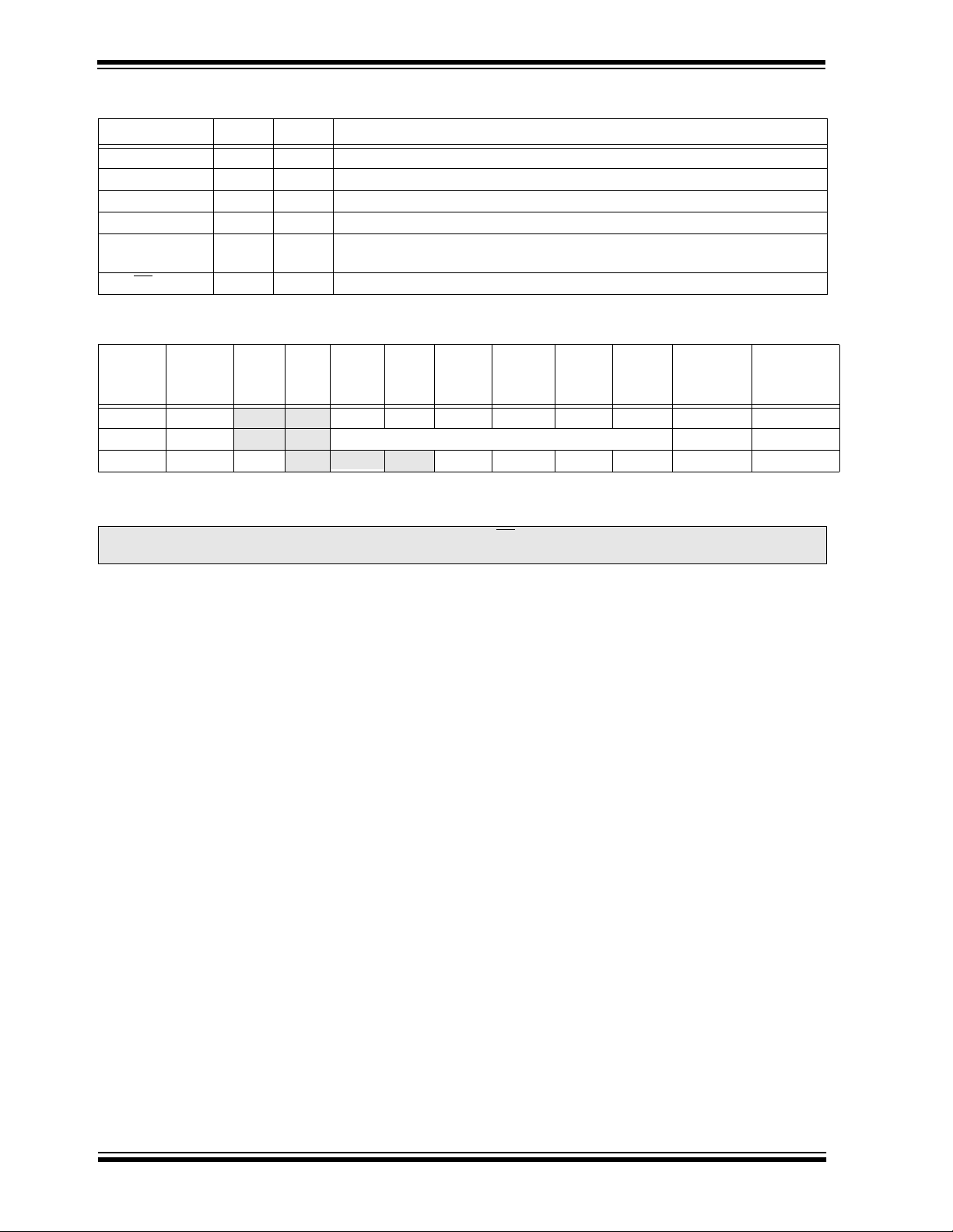
FIGURE 3-1: BLOCK DIAGRAM OF
RA<3:0> AND RA5 PINS
Data
Bus
WR
Port
Data Latch
WR
TRIS
TRIS Latch
RD Port
To A/D Converter
Note 1: I/O pins have protection diodes to VDD and VSS.
CK
CK
QD
Q
QD
Q
RD TRIS
QD
Analog
Input
Mode
EN
VDD
P
N
V
I/O pin
SS
TTL
Input
Buffer
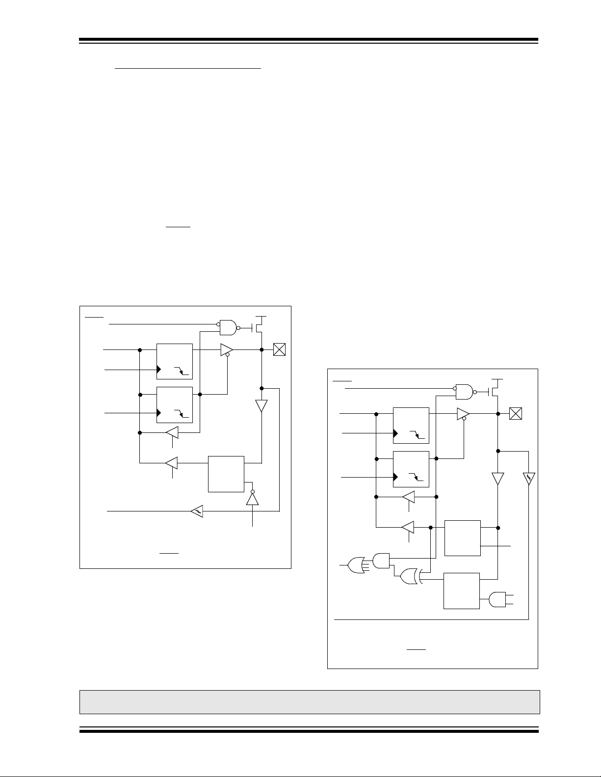
FIGURE 3-2: BLOCK DIAGRAM OF RA4/
T0CKI PIN
Data
Bus
WR
Port
WR
TRIS
RD Port
TMR0 clock input
Note 1: I/O pin has protection diodes to VSS only.
CK
Data Latch
CK
TRIS Latch
RD TRIS
QD
Q
QD
Q
QD
Schmitt
Trigger
Input
Buffer
EN
EN
V
I/O pin
N
SS
(1)
(1)
1999 Microchip Technology Inc.
Preliminary DS30221A-page 23
Page 24
PIC16F872
TABLE 3-1: PORTA FUNCTIONS
Name Bit# Buffer Function
RA0/AN0 bit0 TTL Input/output or analog input
RA1/AN1 bit1 TTL Input/output or analog input
RA2/AN2 bit2 TTL Input/output or analog input
RA3/AN3/VREF bit3 TTL Input/output or analog input or VREF
RA4/T0CKI bit4 ST Input/output or external clock input for Timer0
Output is open drain type
RA5/SS
Legend: TTL = TTL input, ST = Schmitt Trigger input.
TABLE 3-2: SUMMARY OF REGISTERS ASSOCIATED WITH PORTA
Address Name Bit 7 Bit 6 Bit 5 Bit 4 Bit 3 Bit 2 Bit 1 Bit 0
05h PORTA — — RA5 RA4 RA3 RA2 RA1 RA0
85h TRISA — — PORTA Data Direction Register
9Fh ADCON1 ADFM — — — PCFG3 PCFG2 PCFG1 PCFG0
Legend: x = unknown, u = unchanged, - = unimplemented locations read as '0'. Shaded cells are not used by PORTA.
/AN4 bit5 TTL Input/output or slave select input for synchronous serial port or analog input
Value on:
POR,
BOR
--0x 0000 --0u 0000
--11 1111 --11 1111
--0- 0000 --0- 0000
Value on all
other
resets
Note: When using the SSP module in SPI slave mode and SS enabled, the A/D converter must be set to one of
the following modes where PCFG<3:0> = 0100,0101, 011x, 1101, 1110, 1111.
DS30221A-page 24 Preliminary
1999 Microchip Technology Inc.
Page 25
PIC16F872
3.2 PORTB and the TRISB Register
PORTB is an 8-bit wide bi-directional port. The corresponding data direction register is TRISB. Setting a
TRISB bit (=1) will make the correspon ding POR TB pin
an input (i.e., put the corresponding output driver in a
hi-impedance mode). Clearing a TRISB bit (=0) will
make the corresponding PORTB pin an output (i.e., put
the contents of the output latch on the selected pin).
Three pins of PORTB are multiplexed with the Low
Voltage Programming function; RB3/PGM, RB6/PGC
and RB7/PGD. The alternate functions of these pins
are described in the Special Features Section.
Each of the PORTB pins h as a w ea k in ternal p ull -up. A
single control bit ca n turn on all the pull-u ps. This is performed by clea ring bi t RBPU
(OPTION_REG<7>). The
weak pull-up i s autom atically tur ned off when the po rt
pin is configured as an output. The pull-ups are disabled on a Power-on Reset.
FIGURE 3-3: BLOCK DIAGRAM OF
RB<3:0> PINS
V
TTL
Input
Buffer
EN
DD
weak
P
pull-up
I/O
pin
RD Port
(1)
(2)
RBPU
Data Bus
WR Port
WR TRIS
RB0/INT
RB3/PGM
Note 1: I/O pins have diode protection to V
2: To enable weak pull-ups, set the appropriate TRIS bit(s)
and clear the RBPU
Data Latch
QD
CK
TRIS Latch
QD
CK
RD TRIS
RD Port
Schmitt Trigger
Buffer
bit (OPTION_REG<7>).
QD
DD and VSS.
This interrupt can wake the device from SLEEP. The
user, i n the interrupt service routine , can clea r the interrupt in the following manner:
a) Any read or write of PORTB. This will end the
mismatch condition.
b) Clear flag bit RBIF.
A mismatch condition will continue to set flag bit RBIF.
Reading PORTB will end the mismatch condition and
allow flag bit RBIF to be cleared.
The interrupt on change feature is recommended for
wake-up on key depression operation and opera tions
where PORTB is only used for the interrupt on change
feature. Polling of PORTB is not recommended while
using the interrupt on change feature.
This interrupt on mismatch feature, together with software configurable pull-ups on these four pins, allow
easy interface to a keypad and make it possible for
wake-up on key-depression. Refer to the Embedded
Control Handbook,
(AN552).
Stroke”
“Implementing Wake-Up on Key
RB0/INT is an external interrupt inp ut pin and is confi gured using the INTEDG bit (OPTION_REG<6>).
RB0/INT is discussed in detail in Section 11.10.1.
FIGURE 3-4: BLOCK DIAGRAM OF
RB<7:4> PINS
V
EN
TTL
Input
Buffer
DD
P
weak
pull-up
I/O
pin
Buffer
Q1
(1)
ST
RBPU
Data Bus
WR Port
WR TRIS
Set RBIF
(2)
Data Latch
QD
CK
TRIS Latch
QD
CK
RD TRIS
RD Port
Latch
QD
Four of PORTB’s pins, RB<7:4>, have an interrupt on
change feature. Only pins configured as inputs can
cause this interrupt to occur (i.e., any RB<7:4> pin configured as an output is excluded from the interrupt on
From other
RB<7:4> pins
RB<7:6> in serial programming mode
QD
RD Port
EN
change comparison). The input pins (of RB<7:4>) are
compared with th e o ld value latche d o n the last read of
PORTB. The “mismatch” outputs of RB<7:4> are
OR’ed together to generate the RB Port Change Inter-
Note 1: I/O pins have diode protection to V
2: To enable weak pull-ups, set the appropriate TRIS bit(s)
and clear the RBPU
bit (OPTION_REG<7>).
DD and VSS.
rupt with flag bit RBIF (INTCON<0>).
Note: When using Low Voltage ICSP Programming (LVP) and the pull-ups on PORTB are enabled, bit 3 in the
TRISB register must b e cleared to di sable th e pull-up on RB 3 and ensure the p roper oper ation of the de vice .
1999 Microchip Technology Inc.
Preliminary DS30221A-page 25
Q3
Page 26
PIC16F872
TABLE 3-3: PORTB FUNCTIONS
Name Bit# Buffer Function
RB0/INT bit0 TTL/ST
RB1 bit1 TTL Input/output pin. Internal software programmable weak pull-up.
RB2 bit2 TTL Input/output pin. Internal software programmable weak pull-up.
RB3/PGM bit3 TTL/ST
RB4 bit4 TTL Input/output pin (with interrupt on chang e). Internal so ftw are prog ra mmab l e
RB5 bit5 TTL Input/output pin (with interrupt on chang e). Internal so ftw are prog ra mmab l e
RB6/PGC bit6 TTL/ST
RB7/PGD bit7 TTL/ST
Legend: TTL = TTL input, ST = Schmitt Trigger input.
Note 1: This buffer is a Schmitt Trigger input when configured as the external interrupt or LVP mode.
2: This buffer is a Schmitt Trigger input when used in serial programming mode.
TABLE 3-4: SUMMARY OF REGISTERS ASSOCIATED WITH PORTB
Address Name Bit 7 Bit 6 Bit 5 Bit 4 Bit 3 Bit 2 Bit 1 Bit 0
06h, 106h PORTB RB7 RB6 RB5 RB4 RB3 RB2 RB1 RB0 xxxx xxxx uuuu uuuu
86h, 186h TRISB PORTB Data Direction Register 1111 1111 1111 1111
81h, 181h OPTION_REG RBPU
Legend: x = unknown, u = unchanged. Shaded cells are not used by PORTB.
(1)
Input/output pin or external interrupt input. Internal software
programmable weak pull-up.
(1)
Input/output pin or programming pin in LVP mode. Internal software
programmable weak pull-up.
weak pull-up .
weak pull-up .
(2)
Input/output pin (with interrupt on change) or In-Circuit Debugger pin.
Internal software programmable weak pull-up. Serial programming clock.
(2)
Input/output pin (with interrupt on change) or In-Circuit Debugger pin.
Internal software programmable weak pull-up. Serial programming data.
Value on:
POR,
BOR
INTEDG T0CS T0SE PSA PS2 PS1 PS0 1111 1111 1111 1111
Value on all
other
resets
DS30221A-page 26 Preliminary
1999 Microchip Technology Inc.
Page 27
PIC16F872
3.3 PORTC and the TRISC Register
PORTC is an 8-bit wide, bi-directional port. The corresponding data direction register is TRISC. Setting a
TRISC bit (=1) will mak e the corres ponding POR TC pin
an input (i.e., put the corresponding output driver in a
hi-impedance mode). Clearing a TRISC bit (=0) will
make the cor respon ding POR T C pin an output (i .e. , put
the contents of the output latch on the selected pin).
PORTC is mul tiple x ed with se v eral peripheral fun ctions
(Table 3-5). PORTC pins have Schmitt Trigger input
buffers.
2
When the I
can be configured with normal I
C module is enab led, the POR TC (3:4) pins
2
C levels or with
SMBUS levels by using the CKE bit (SSPSTAT<6>).
When enabling peripheral functions, care should be
taken in defining TRIS bits for each PORTC pin. Some
periphe rals override the TRIS bit to make a pin an output, while other peripherals override the TRIS bit to
make a pin an input. Since the TRIS bit override is in
effect while the peripheral is enabled, read-modifywrite instructions (BS F, BCF, XORWF) with TRISC as
destination shou ld be a voi ded. The us er should refe r to
the corresponding peripheral section for the correct
TRIS bit settings.
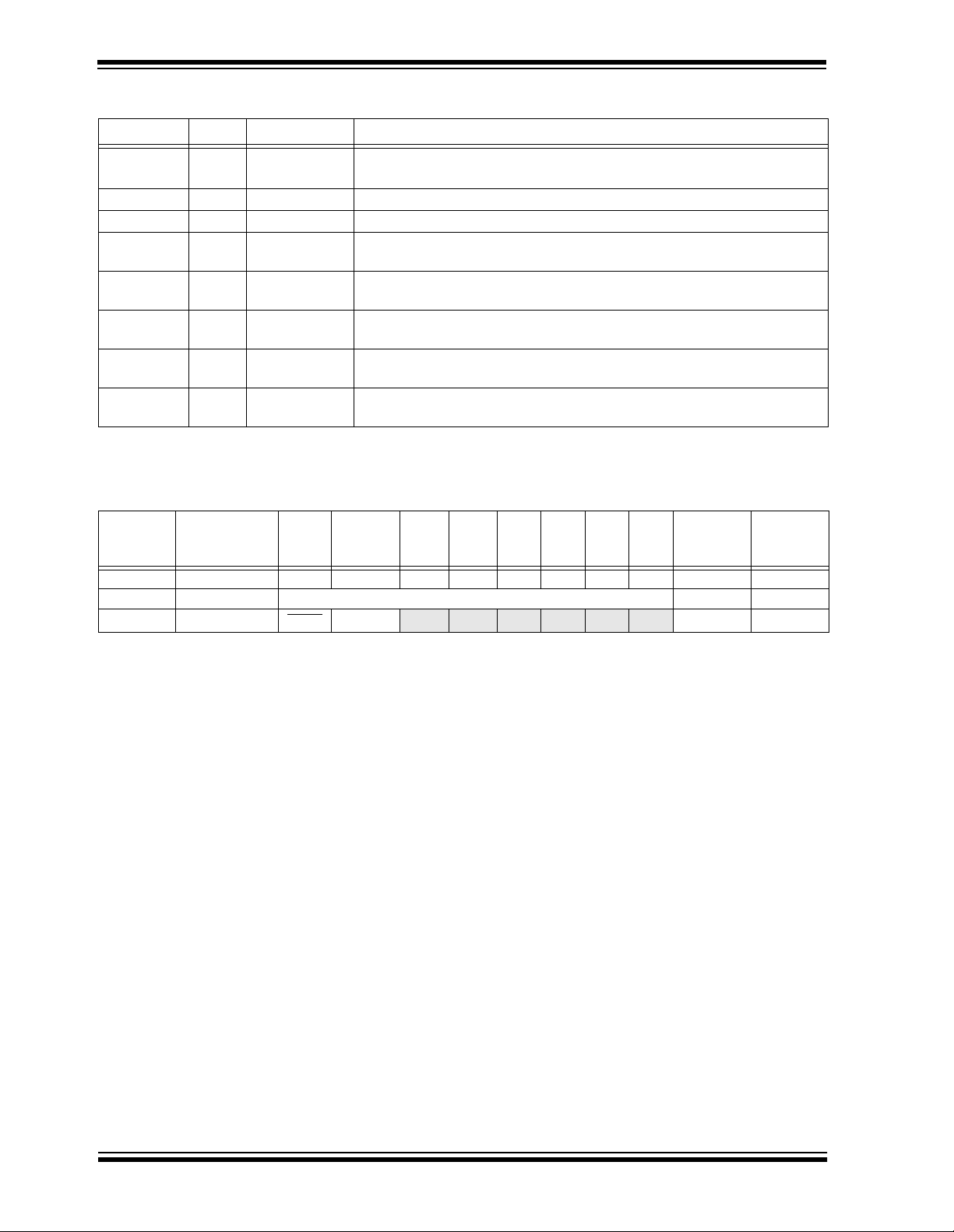
FIGURE 3-5: P ORTC BLOCK DIAGRAM
(PERIPHERAL OUTPUT
OVERRIDE) RC<0:2>
RC<5:7>
Port/Peripheral Select
Peripheral Data Out
Data Bus
WR
Port
WR
TRIS
Peripheral
(3)
OE
(2)
QD
Q
CK
Data Latch
QD
CK
TRIS Latch
RD TRIS
V
Schmitt
Trigger
N
VSS
DD
P
I/O
(1)
pin
0
1
Q
QD
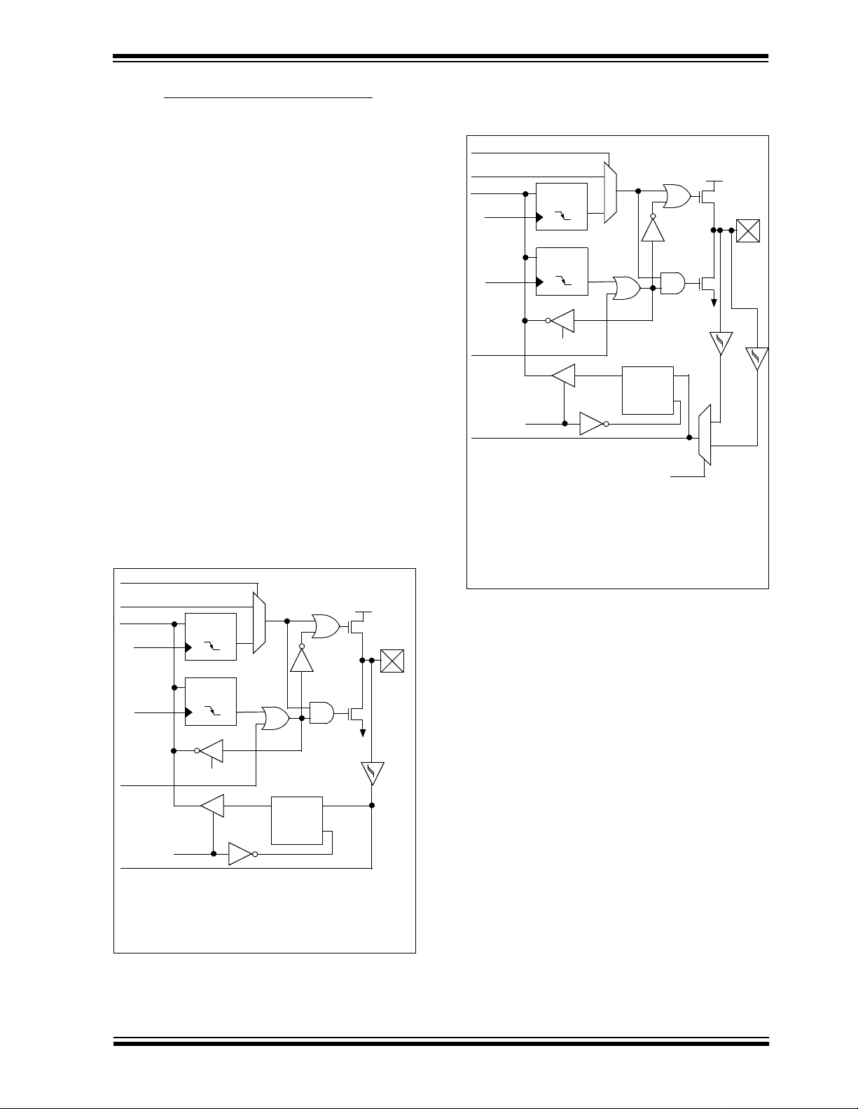
FIGURE 3-6: PORTC BLOCK DIAGRAM
(PERIPHERAL OUTPUT
OVERRIDE) RC<3:4>
CK
Data Latch
CK
TRIS Latch
RD TRIS
RD
Port
(2)
V
Schmitt
Trigger
N
Vss
0
1
DD
P
Schmitt
Trigger
with
SMBus
levels
0
QD
1
Q
QD
Q
QD
EN
CKE
SSPSTAT<6>
Port/Peripheral Select
Peripheral Data Out
Data Bus
WR
Port
WR
TRIS
Peripheral
(3)
OE
SSPl Input
Note 1: I/O pins have diode protection to VDD and VSS.
2: Port/Peripheral select signal selects between port
data and peripheral output.
3: Peripheral OE (output enable) is only activated if
peripheral select is active.
I/O
pin
(1)
RD
Port
Peripheral Input
EN
Note 1: I/O pins have diode protection to VDD and VSS.
2: Port/Peripheral select signal selects between port
data and peripheral output.
3: Peripheral OE (output enable) is only activated if
peripheral select is active.
1999 Microchip Technology Inc.
Preliminary DS30221A-page 27
Page 28
PIC16F872
TABLE 3-5: PORTC FUNCTIONS
Name Bit# Buffer Type Function
RC0/T1OSO/T1CKI bit0 ST Input/output port pin or Timer1 oscillator output/Timer1 clock input.
RC1/T1OSI bit1 ST Input/output port pin or Timer1 oscillator input.
RC2/CCP1 bit2 ST Input/output port pin or Capture1 input/Compare1 output/PWM1
output.
RC3/SCK/SCL bit3 ST RC3 can also be the synchronous serial clock for both SPI and I
modes.
RC4/SDI/SDA bit4 ST RC4 can also be the SPI Data In (SPI mode) or data I/O (I
RC5/SDO bit5 ST Input/output port pin or Synchronous Serial Port data output.
RC6 bit6 ST Input/output port pin.
RC7 bit7 ST Input/output port pin.
Legend: ST = Schmitt Trigger input.
TABLE 3-6: SUMMARY OF REGISTERS ASSOCIATED WITH PORTC
Value on:
Address Name Bit 7 Bit 6 Bit 5 Bit 4 Bit 3 Bit 2 Bit 1 Bit 0
07h PORTC RC7 RC6 RC5 RC4 RC3 RC2 RC1 RC0
87h TRISC PORTC Data Direction Register
Legend: x = unknown, u = unchanged.
POR,
BOR
xxxx xxxx uuuu uuuu
1111 1111 1111 1111
2
2
C mode).
Value on all
other resets
C
DS30221A-page 28 Preliminary
1999 Microchip Technology Inc.
Page 29

PIC16F872
4.0 DATA EEPROM AND FLASH PROGRAM MEMORY
The Data EEPROM and FLASH Program Memory are
readable an d writab le during normal oper at ion o v e r the
entire VDD ra nge. A bulk eras e operation may not be
issued from user code (which includes removing code
protection). The data memory is not dire ctly m apped in
the register file space. Instead, it is indirectly
addressed through the Special Function Registers
(SFR).
There are six SFRs used to r ead and w rite the prog ram
and data EEPROM memory. These registers are:
• EECON1
• EECON2
• EEDATA
• EEDATH
• EEADR
• EEADRH
The EEPROM data memory allo ws byte read and write .
When interfacing to the data memory block, EEDATA
holds the 8-bit data f or read/write and EEA DR holds the
address of the EEPROM location being accessed. The
registers EEDATH and EEADRH are not used for data
EEPROM access. The PIC16F 872 de vice has 64 bytes
of data EEPROM with an address range from 0h to
3Fh.
The EEPROM data memory is rated for high erase/
write cycles. The write tim e is co ntro lle d by an on-chi p
timer . The writ e time will v a ry with v oltag e and te mperature, as well as from chip-to-chip. Please refer to the
specifications for exact limits.
The program m emory allows word re ads and writes.
Program memory access allows for checksum calculation and ca libr ation table sto rage. A byt e or wo rd w r ite
automatically erases the location and writes the new
data (erase before write). Writing to program memory
will cease opera tion until the writ e is complete. T he program memory cannot be accessed during the write,
therefore c ode c ann ot execut e . During the write oper ation, the oscillator continues to clock the peripherals,
and therefore, they continue to operate. Interrupt
events will be detected and essentially “queued” until
the write is completed. When the write completes, the
next instruction in the pipeline is executed and the
branch to the interrupt vector address will occur.
When interfacing to the program memory block, the
EEDATH:EEDATA registers form a two byte word,
which holds the 14-bit data for read/write. The
EEADRH:EEADR registers form a two byte word,
which holds the 13-bit address of the FLASH location
being accessed. The PIC16F872 device has 2K w ords
of program FLASH with an address range from 0h to
7FFh. The unused upper bits in both the EEDATH and
EEDATA registers all read as “0’s”.
The value written to pro gram m emory does not need to
be a valid instruction. Therefore, up to 14-bit numbers
can be stored in memory for use as calibration parameters, serial numbers, packed 7-bit ASCII, etc. Executing a program memory location containing data that
forms an invalid instruction results in a NOP.
4.1 EEADR
The address registers can address up to a maxim um of
256 bytes of data EEPROM or up to a maximum of 8K
words of program FLASH. However, the PIC16F872
has 64 bytes of data EEPROM and 2K words of program FLASH.
When selecting a program address value, the MSByte
of the address is written to the EEADRH register and
the LSByte is written to the EEADR register. When
selecting a data address value, only the LSByte of the
address is written to the EEADR register.
On the PIC16F872 device, the upper two bits of the
EEADR must always be cleared to prevent inadvertent
access to the wrong location in data EEPROM. This
also applies to the program memory. The upper five
MSbits of EEAD RH must always be clear dur ing program FLASH access.
4.2 EECON1 and EECON2 Registers
EECON1 is the control register for memory accesses.
EECON2 is not a physical register. Reading EECON2
will read all '0's. The EECON2 register is used
exclusively in the memory write sequence.
Control bit EEPGD determines if the access will be a
program or a data memory access. When clear, any
subsequent operations will operate on the data memory . Whe n set, any subs equen t oper ations will o per ate
on the program memory.
Control bits RD and WR initiate read and write operations, respectively. These bits cannot be cleared, only
set, in software. They are cleared in hardware at the
completion of the read or write operation. The inability
to clear the WR bit in software prevents the accidental
or premature termination of a write operation.
The WREN bit, when set, will allow a write operation.
On power-up , the WR EN bit is clear . The WRERR bit i s
set when a write operation is interrupted by a MCLR
reset or a WD T ti me-out rese t during n ormal oper atio n.
In these situations, following reset, the user can check
the WRERR bit and rewrite the location. The value of
the data and address registers and the EEPGD bit
remains unchanged.
Interrupt flag bit EEIF, in the PIR2 register, i s set whe n
write is complete. It must be cleared in software.
1999 Microchip Technology Inc.
Preliminary DS30221A-page 29
Page 30

PIC16F872
REGISTER 4-1: EECON1 REGISTER (ADDRESS 18Ch)
R/W-x U-0 U-0 U-0 R/W-x R/W-0 R/S-0 R/S-0
EEPGD — — — WRERR WREN WR RD R = Readable bit
bit7 bit0
bit 7: EEPGD: Program / Data EEPROM Select bit
1 = Accesses Program memory
0 = Accesses data memory
(This bit cannot be changed while a read or write operation is in progress)
bit 6-4: Unimplemented: Read as '0'
bit 3: WRERR: EEPROM Error Flag bit
1 = A write operation is prematurely terminated
(any MCLR
0 = The write operation completed
bit 2: WREN: EEPROM Write Enable bit
1 = Allows write cycles
0 = Inhibits write to the EEPROM
bit 1: WR: Write Control bit
1 = initiates a write cycle. (The bit is cleared by hardware once write is complete.) The WR bit can only
be set (not cleared) in software.
0 = Write cycle to the EEPROM is complete
bit 0: RD: Read Control bit
1 = Initiates an EEPROM read RD is cleared in hardware. The RD bit can only be set (not cleared) in
software.
0 = Does not initiate an EEPROM read
reset or any W DT reset during normal operation)
W = Writable bit
U = Unimplemented bit,
read as ‘0’
- n= Value at POR reset
DS30221A-page 30 Preliminary
1999 Microchip Technology Inc.
Page 31

PIC16F872
4.3 Reading the Data EEPROM Memory
T o read a data memory locatio n, the user m ust write the
address to the EEADR register, clear the EEPGD control bit (EECON1<7>) and then set control bit RD
(EECON1<0>). The data is available in the very next
instruction cycle of the EEDATA register, therefore it
can be read by the next instruction. EEDATA will hold
this value until another read operation or until it is written to by the user (during a write operation).
4.4 Writing to the Data EEPR OM Memory
To wr ite an EEPROM data location, the address must
first be written to the EEADR register and the data w ritten to the EEDATA register. Then the sequence in
Example 4-2 must be followed to initi ate the write cycle.
EXAMPLE 4-2: DATA EEPROM WRITE
BSF STATUS, RP1 ;
BCF STATUS, RP0 ; Bank 2
MOVLW DATA_EE_ADDR ;
MOVWF EEADR ; Data Memory Address to write
MOVLW DATA_EE_DATA ;
MOVWF EEDATA ; Data Memory Value to write
BSF STATUS, RP0 ; Bank 3
BCF EECON1, EEPGD ; Point to DATA memory
BSF EECON1, WREN ; Enable writes
BCF INTCON, GIE ; Disable Interrupts
MOVLW 55h ;
Required MOVWF EECON2 ; Write 55h
Sequence MOVLW AAh ;
MOVWF EECON2 ; Write AAh
BSF EECON1, WR ; Set WR bit to begin write
BSF INTCON, GIE ; Enable Interrupts
SLEEP ; Wait for interrupt to signal write complete
BCF EECON1, WREN ; Disable writes
The write will not initiate if the above sequence is not
exactly followed (write 55h to EECON2, write AAh to
EECON2, then set WR bit) for each byte. It is strongly
recommended that interrupts be disabled during this
code segment.
Additionally, the WREN bit in EECON1 must be set to
enable writes. This mechanism prevents accidental
writes to data EEPROM due to unexpected code execution (i.e., runaway programs). The WREN bit should
be kept clear at all times, except when updating the
EEPROM. The WREN bit is not cleared by hardware
After a write sequence has been initiated, clearing the
WREN bit will not aff ect the current write cycle . The WR
bit will be inhibited from be ing set unles s the WREN bit
EXAMPLE 4-1: DATA EEPROM READ
BSF STATUS, RP1 ;
BCF STATUS, RP0 ;Bank 2
MOVLW DATA_EE_ADDR ;
MOVWF EEADR ;Data Memory Address to read
BSF STATUS, RP0 ;Bank 3
BCF EECON1, EEPGD ;Point to DATA memory
BSF EECON1, RD ;EEPROM Read
BCF STATUS, RP0 ;Bank 2
MOVF EEDATA, W ;W = EEDATA
is set. The WREN bit m ust be set on a previous instruction. Both WR and WREN ca nno t be set with the sam e
instruction.
At the completion of the write cycle, the WR bit is
cleared in hardware and the EEPROM Write Compl ete
Interrupt Flag bit (EEIF) is set. EEIF m ust be cl eared by
software.
1999 Microchip Technology Inc.
Preliminary DS30221A-page 31
Page 32

PIC16F872
4.5 Reading the FLASH Program Memory
A program me mory location ma y be rea d by writing tw o
bytes of the address to the EEADR and EEADRH registers, setting the EEPGD control bit (EECON1<7>)
and then setting control bit RD (EECON1<0>). Once
the read control bit is set, the microcontroller will use
the next two instruction cycles to read the data. The
EXAMPLE 4-3: FLASH PROGRAM READ
BSF STATUS, RP1 ;
BCF STATUS, RP0 ; Bank 2
MOVLW ADDRH ;
MOVWF EEADRH ; MSByte of Program Address to read
MOVLW ADDRL ;
MOVWF EEADR ; LSByte of Program Address to read
BSF STATUS, RP0 ; Bank 3
BSF EECON1, EEPGD ; Point to PROGRAM memory
Required BSF EECON1, RD ; EEPROM Read
Sequence
NOP ; memory is read in the next two cycles after BSF EECON1,RD
NOP ;
BCF STATUS, RP0 ; Bank 2
data is available in the EEDATA and EEDATH registers
after the second NOP instruction. Therefore, it can be
read as two bytes in the following instructions. The
EEDATA and EEDATH registers will hold this value
until another read o peration or u ntil it is written to by the
user (during a write operation).
MOVF EEDATA, W ; W = LSByte of Program EEDATA
MOVF EEDATH, W ; W = MSByte of Program EEDATA
DS30221A-page 32 Preliminary
1999 Microchip Technology Inc.
Page 33

PIC16F872
4.6 Writing to the FLASH Program Memory
When the PIC16F872 is fully code protected or not
code protected, a w ord of the F LASH prog ram me mory
may be written provided the WRT configuration bit is
set. If the PIC16F 872 is partially code p rotected, then a
word of FLASH program memory may be written if the
word is in a non-code protected segment of memory
and the WRT co nfi guration bit is se t. To write a FLASH
program location, the first two bytes of the address
must be written to the EEADR and EEADRH registers
and two bytes of the data to the EEDATA and EEDATH
registers, set the EEPGD control bit (EECON1<7>),
EXAMPLE 4-4: FLASH PROGRAM WRITE
BSF STATUS, RP1 ;
BCF STATUS, RP0 ; Bank 2
MOVLW ADDRH ;
MOVWF EEADRH ; MSByte of Program Address to read
MOVLW ADDRL ;
MOVWF EEADR ; LSByte of Program Address to read
MOVLW DATAH ;
MOVWF EEDATH ; MS Program Memory Value to write
MOVLW DATAL ;
MOVWF EEDATA ; LS Program Memory Value to write
BSF STATUS, RP0 ; Bank 3
BSF EECON1, EEPGD ; Point to PROGRAM memory
BSF EECON1, WREN ; Enable writes
BCF INTCON, GIE ; Disable Interrupts
MOVLW 55h ;
Required MOVWF EECON2 ; Write 55h
Sequence MOVLW AAh ;
MOVWF EECON2 ; Write AAh
BSF EECON1, WR ; Set WR bit to begin write
NOP ; Instructions here are ignored by the microcontroller
NOP
; Microcontroller will halt operation and wait for
; a write complete. After the write
; the microcontroller continues with 3rd instruction
BSF INTCON, GIE ; Enable Interrupts
BCF EECON1, WREN ; Disable writes
and then set control bit WR (EECON1<1>). The
sequence in Example4-4 must be follo wed to initiate a
write to program memory.
The microcontroller will then halt internal operations
during the next two instruction cycles for the T
PEW
(parameter D133) in which the write takes place. This
is not SLEEP mode, as the clocks and peripherals will
continue to run. Therefore, the two instructions follow-
ing the “BSF EECON, WR” should be NOP instructions.
After the write cycle, the microcontroller will resume
operation with the 3rd instruction after the EECON1
write instruction.
1999 Microchip Technology Inc.
Preliminary DS30221A-page 33
Page 34
PIC16F872
4.7 Write Verify
Depending on the application, good programming
practice may dictate that the value written to the memory should be verified against the original value. This
should be used in applications where excessive writes
can stress bits near the specification limit.
Generally a write failure will be a bit which was written
as a ’1’, but reads back as a ’0’ (due to leakage off the
bit).
4.8 Protection Against Spurious Write
4.8.1 EEPROM DATA MEMORY There are conditions when the device may not want to
write to the data EEPROM memory. To protect against
spurious EEPROM writes, various mechanisms have
been built-in. On power-up, the WREN bit is cleared.
Also, the Power-up Timer (72 ms duration) prevents
EEPROM write.
The write initiate sequence and the WREN bi t together
help prevent an accidental write during brown-out,
power glitch, or software malfunction.
4.8.2 PROGRAM FLASH MEMORY To protect against spurious writes to FLASH program
memory, the WRT bit in the configuration word may be
programmed to ‘0’ to prevent writes. The write initiate
sequence must also be followed. WRT and the configuration word c annot be prog rammed b y user code, onl y
through the use of an external programmer.
4.9 Operation during Code Protect
Each reprogramm able memory bloc k has its o w n cod e
protect mechanism. External Read and Write operations are disabled if either of these mechanisms are
enabled.
4.9.1 DATA EEPROM MEMORY The microcontroller itself c an both re ad and writ e to the
internal Data EEPROM, regardless of the state of the
code protect configuration bit.
4.9.2 PROGRAM FLASH MEMORY The microcontroller can read and execute instructions
out of the internal FLASH progra m memory, regardless
of the state of the c ode protect configur a tio n b its. However, the WRT configuration bit and the code protect
bits have different effects on writing to program memory. Table 4-1 shows the various configurations and
status of reads and writes . To erase the WRT o r code
protection bits in the configuration word requires that
the device be fully erased.
Note: The PIC16F872 devices can perform self
writes to any location in program memory
when not code protected or fully code
protected.
TABLE 4-1: READ/WRITE STATE OF INTERNAL FLASH PROGRAM MEMORY
Configuration Bits
Memory Location
CP1 CP0 WRT
001All program memory Yes Yes No No
000All program memory Yes No No No
010Unprotected areas Yes No Yes No
010Protected areas Yes No No No
011Unprotected areas Yes Yes Yes No
011Protected areas Yes No No No
100Unprotected areas Yes No Yes No
100Protected areas Yes No No No
101Unprotected areas Yes Yes Yes No
101Protected areas Yes No No No
110All program memory Yes No Yes Yes
111All program memory Yes Yes Y es Yes
Internal
Read
Internal
Write
ICSP Read ICSP Write
DS30221A-page 34 Preliminary
1999 Microchip Technology Inc.
Page 35

PIC16F872
TABLE 4-2: REGISTERS ASSOCIATED WITH DATA EEPROM/PROGRAM FLASH
Value on:
AddressNameBit 7Bit 6Bit 5Bit 4Bit 3Bit 2Bit 1Bit 0
0Bh, 8Bh,
10Bh, 18Bh
10Dh EEADR EEPROM address register xxxx xxxx uuuu uuuu
10Fh EEADRH —————EEPROM address high xxxx xxxx uuuu uuuu
10Ch EEDATA EEPROM data resister xxxx xxxx uuuu uuuu
10Eh EEDATH — — EEPROM data resister high xxxx xxxx uuuu uuuu
18Ch EECON1 EEPGD — — — WRERR WREN WR
18Dh EECON2 EEPROM control resister2 (not a physical resister)
8Dh PIE2
0Dh PIR2
Legend: x = unknown, u = unchanged, r = reserved, - = unimplemented read as ’0’. Shaded cells are not used by the
Note 1: These bits are reser ved; always maintain these bits clear.
INTCON GIE PEIE T0IE INTE RBIE T0IF INTF RBIF 0000 000x 0000 000u
RD x--- x000 x--- u000
— (1) — EEIE BCLIE — — (1) -r-0 0--r -r-0 0--r
— (1) — EEIF BCLIF — — (1) -r-0 0--r -r-0 0--r
Timer1 module.
POR,
BOR
Value on
all other
resets
1999 Microchip Technology Inc.
Preliminary DS30221A-page 35
Page 36

PIC16F872
NOTES:
DS30221A-page 36 Preliminary
1999 Microchip Technology Inc.
Page 37

PIC16F872
5.0 TIMER0 MODUL E
The Timer0 module timer/co unter has th e fol lowing f eatures:
• 8-bit timer/counter
• Readable and writable
• 8-bit software programmable prescaler
• Internal or external clock select
• Interrupt on overflow from FFh to 00h
• Edge select for external clock
Figure 5-1 is a block diagram of the Timer0 module and
Counter mode is selected by setting bit T0CS
(OPTION_REG<5>). In counter mode, Timer0 will
increment either on every ri sing or falling edge of pin
RA4/T0CKI. The incrementing edge is determined by
the Timer0 Source Edge Select bit T0SE
(OPTION_REG<4>). Clearing bit T0SE selects the rising edge. Restrictions on the external clock input are
discussed in detail in S ection 5.2.
The prescaler is mutually exclusively shared between
the Timer0 module and the watchdog timer. The prescaler is not readab le o r writab le . Sec tion5.3 details the
operation of the prescale r.
the prescal e r s ha r ed with the WDT.
Additional information on th e Timer0 module is avail-
able in the PICmicro™ Mid-Range MCU Family Reference Manual (DS33023).
Timer mode is selected by clearing bit T0CS
(OPTION_REG<5>). In timer mode, the Timer0 module will increment eve ry instruct ion cy cl e (w it hou t prescaler). If the TMR0 register is written, the increment is
inhibited for the following two instruction cycles. The
user can work around this by writing an adjusted value
5.1 Timer0 Interrupt
The TMR0 interrupt is generated when the TMR0 register overflows from FFh to 00 h. This overflow sets bit
T0IF (INTCON<2>). The interrupt can be masked by
clearing bit T0IE (INTCON<5>). Bit T0IF must be
cleared in softwa re b y the T imer0 mo dule interrupt s ervice routine before re-enabling this interrupt. The
TMR0 interrupt cannot awaken the processor from
SLEEP since the timer is shut off during SLEEP.
to the TMR0 register.
FIGURE 5-1: BLOCK DIAGRAM OF THE TIMER0/WDT PRESCALER
CLKOUT (= F
RA4/T0CKI
Pin
Watchdog
Timer
WDT Enable bit
OSC/4)
T0SE
Data Bus
M
0
U
X
1
T0CS
0
M
U
1
X
PSA
8-bit Prescaler
8 - to - 1MUX
0
Time-out
PRESCALER
8
M U X
WDT
1
M
U
0
X
PSA
1
PSA
SYNC
2
Cycles
PS<2:0>
8
TMR0 reg
Set Flag Bit T0IF
on Overflow
Note: T0CS, T0SE, PSA, PS<2:0> are (OPTION_REG<5:0>).
1999 Microchip Technology Inc.
Preliminary DS30221A-page 37
Page 38

PIC16F872
5.2 Using Timer0 with an External Clock
module means that there is no prescaler for the watchdog timer, and vice-v ersa. This prescaler is not readab le
When no prescaler is used, the external clock input is
the same as the prescaler output. The synchronization
of T0CKI with the internal phase clocks is accomplished by sam pling the pres caler output o n the Q2 and
Q4 cycles of the internal phase clocks. Therefore, it is
necessary for T0CKI to be high for at least 2T
a small RC delay of 20 ns) and low for at least 2T
OSC (and
OSC
(and a small RC delay of 20 ns). Refer to the electrical
specification of the desired device.
or writable (see Figure 5-1).
The PSA and PS<2:0> bits (OPTION_REG<3:0>) deter-
mine the prescaler assignment and prescale ratio.
When assigned to the Timer0 module, all instructions
writing to the TMR0 register (i.e., CLRF
BSF
1,x...., etc.) will clear the prescaler. When
1, MOVWF 1,
assigned to WDT, a CLRWDT instructio n will clear the
prescaler along with the Watchdog Timer. The prescaler is not readable or writable.
5.3 Prescaler
There is only one prescaler available, which is mutually
exclusively shared between the Timer0 module and the
watchdog timer. A prescaler assignment for the Timer0
Note: Writing to TMR0, when the prescaler is
assigned to Timer0, will clear the prescaler
count, but will not change the prescaler
assignment.
REGISTER 5-1: OPTION_REG REGISTER
R/W-1 R/W-1 R/W-1 R/W-1 R/W-1 R/W-1 R/W-1 R/W-1
U INTEDG T0CS T0SE PSA PS2 PS1 PS0
RBP
bit 7 bit 0
bit 7: RBPU
bit 6: INTEDG
bit 5: T0CS: TMR0 Clock Source Select bit
1 = Transition on T0CKI pin
0 = Interna l instruction cycle clock (CLKOUT)
bit 4: T0SE: TMR0 Source Edge Select bit
1 = Increment on high-to-low transition on T0CKI pi n
0 = Increment on low-to-high transition on T0CKI pin
bit 3: PSA: Prescaler Assignment bit
1 = Prescaler is assigned to the WDT
0 = Prescaler is assigned to the Timer0 module
bit 2-0: PS<2:0>: Prescaler Rate Select bits
Bit Value TMR0 Rate WDT Rate
000
001
010
011
100
101
110
111
1 : 2
1 : 4
1 : 8
1 : 16
1 : 32
1 : 64
1 : 128
1 : 256
1 : 1
1 : 2
1 : 4
1 : 8
1 : 16
1 : 32
1 : 64
1 : 128
Note: To avoid an unintended de vice RESET, the instruction sequence show n in the PICmicro™ Mi d-Range MCU
Family Reference Manual (DS33023) must be executed when changing the prescaler assignment from
Timer0 to the WDT. This sequence must be followed even if the WDT is disabled.
R = Readable bit
W = Writable bit
U = Unimplemented bit,
read as ‘0’
- n = Value at POR reset
DS30221A-page 38 Preliminary
1999 Microchip Technology Inc.
Page 39

PIC16F872
TABLE 5-1: REGISTERS ASSOCIATED WITH TIMER0
Value on:
Address Name Bit 7 Bit 6 Bit 5 Bit 4 Bit 3 Bit 2 Bit 1 Bit 0
01h,101h TMR0 Timer0 module’s register xxxx xxxx uuuu uuuu
0Bh,8Bh,
10Bh,18Bh
81h,181h OPTION_REG
Legend: x = unknown, u = unchanged, - = unimplemented locations read as '0'. Shaded cells are not used by Timer0.
INTCON GIE PEIE T0IE
RBPU INTEDG T0CS T0SE PSA PS2 PS1 PS0 1111 1111 1111 1111
INTE RBIE T0IF INTF RBIF 0000 000x 0000 000u
POR,
BOR
Value on all
other resets
1999 Microchip Technology Inc.
Preliminary DS30221A-page 39
Page 40

PIC16F872
NOTES:
DS30221A-page 40 Preliminary
1999 Microchip Technology Inc.
Page 41

PIC16F872
6.0 TIMER1 MODUL E
The Timer1 module is a 1 6-bi t ti me r/counter consisting
of two 8-bit registers (TMR1H and TMR1L), which are
readable and writable. The TMR1 Register pair
(TMR1H:TMR1L) increments from 0000h to FFFFh
and rolls ove r to 0000h. The TMR1 Int errupt, if enabled,
is generated on overflow, which is latched in interrupt
flag bit TMR1IF (PIR1<0>). This interrupt can be
enabled/disabled by setting/clearing TMR1 interrupt
enable bit TMR1IE (PIE1<0>).
Timer1 can operate in one of two modes:
•As a timer
•As a counter
The operating mode is determined by the clock select
bit, TMR1CS (T1CON<1>).
In timer mode, Timer1 increments every instruction
cycle. In coun ter mo de, it in crement s on every risi ng
edge of the external clock input.
Timer1 can be enabled/disabled by setting/clearing
control bit TMR1ON (T1CON<0> ) .
Timer1 also has an in ternal “reset input ”. This reset can
be generated by the CCP module (Section 8.0).
Register 6-1 shows the Timer1 control register.
When the Timer1 oscillator is enabled (T1OSCEN is
set), the RC1/T1OSI and RC0/T1OSO/T1CKI pins
become inputs. That is, the TRISC<1:0> value is
ignored.
Additional information on timer modules is available in
the PICmicro™ Mid-range MCU Family Reference
Manual (DS33023).
REGISTER 6-1: T1CON: TIMER1 CONTROL REGISTER (ADDRESS 10h)
U-0 U-0 R/W-0 R/W-0 R/W-0 R/W-0 R/W-0 R/W-0
— — T1CKPS1 T1CKPS0 T1OSCEN T1SYNC TMR1CS TMR1ON
bit7 bit0
bit 7-6: Unimplemented: Read as '0'
bit 5-4: T1CKPS<1:0>: Timer1 Input Clock Prescale Select bits
11 = 1:8 Prescale value
10 = 1:4 Prescale value
01 = 1:2 Prescale value
00 = 1:1 Prescale value
bit 3: T1OSCEN: Timer1 Oscillator Enable Control bit
1 = Oscillator is enabled
0 = Oscillator is shut off (The oscillator inverter is turned off to eliminate power drain)
bit 2: T1SYNC
TMR1CS = 1
1 = Do not synchronize external clock input
0 = Synchronize external clock input
T
This bit is ignored. Timer1 uses the internal clock when TMR1CS = 0.
bit 1: TMR1CS: Timer1 Clock Source Select bit
1 = External clock from pin RC0/T1OSO/T1CKI (on the rising edge)
0 = Internal clock (F
bit 0: TMR1ON: Timer1 On bit
1 = Enables Timer1
0 = Stops Timer1
: Timer1 External Clock Input Synchronization Control bit
MR1CS = 0
OSC/4)
R = Readable bit
W = Writable bit
U = Unimplemented bit,
read as ‘0’
- n = Value at POR reset
1999 Microchip Technology Inc.
Preliminary DS30221A-page 41
Page 42

PIC16F872
6.1 Timer1 Operation in Timer Mode
Timer mode is selected by clearing the TMR1CS
(T1CON<1>) bit. In this mode, the input clock to the
timer is FOSC/4. The synchronize control bit T1SYNC
(T1CON<2>) has no effect since the internal clock is
always in sync.
FIGURE 6-1: TIMER1 INCREMENTING EDGE
T1CKI
(Default high)
T1CKI
(Default low)
Note: Arrows indicate counter increments.
6.3 Timer1 Operation in Synchronized Counter Mode
Counter mode is selected by setting bit TMR1CS. In
this mode, the time r increment s on ev ery rising edge of
clock input on pin RC1/T1OSI, when bit T1OSCEN is
set, or on pin RC0/T1O SO/T1C KI , when bi t T1O SC EN
is cleared.
6.2 Timer1 Counter Operation
Timer1 may operate in asynchronous or usynchronous
mode depending on the setting of the TMR1CS bit.
When Timer1 is being incremented via an external
source, incr ements occur on a rising edge. After Timer1
is enabled in counter mode, the module must first have
a falling edge before the counter begins to increment.
If T1SYNC
synchronized with internal phase clocks. The synchronization is done after the prescaler stage. The prescaler stage is an asynchronous ripple-counter.
In this configuration, during SLEEP mode, Timer1 will
not increment even if the external clock is present,
since the synchronization circuit is shut off. The prescaler however will continue to increment.
is cleared, then the external clock input is
FIGURE 6-2: TIMER1 BLOCK DIAGRAM
Set flag bit
TMR1IF on
Overflow
RC0/T1OSO/T1CKI
RC1/T1OSI
Note 1: When the T1OSCEN bit is cleared, the inverter is turned off. This eliminates power drain.
(2)
2: For the PIC16F872, the Schmitt Trigger is not implemented in external clock mode.
TMR1H
T1OSC
TMR1
TMR1L
T1OSCEN
Enable
Oscillator
(1)
(2)
FOSC/4
Internal
Clock
TMR1ON
on/off
1
0
TMR1CS
0
1
T1SYNC
Prescaler
1, 2, 4, 8
2
T1CKPS<1:0>
Synchronized
clock input
Synchronize
det
Q Clock
DS30221A-page 42 Preliminary
1999 Microchip Technology Inc.
Page 43

PIC16F872
6.4 Timer1 Operation in Asynchronous Counter Mode
If control bit T1SYNC (T1CON<2>) is set, the external
clock input is not synchronized. The timer continues to
increment asynchronous to the internal phase clocks.
The timer will continue to run during SLEEP and can
generate an i nterrupt on overflow, which will wake-up
the processor. However, special precautions in software are needed to read/write the time r (Section 6.4.1).
In asynchronous counter mode, Timer1 can not be used
as a time-base for capture or compare operations.
6.4.1 READING AND WRITING TIMER1 IN ASYNCHRONOUS COUNTER MODE
Reading TMR1H or TMR1L while the timer is running
from an external asynchronous clock will guarantee a
valid read (taken care of in hardware). However, the
user should keep in mind that reading the 16-bit timer
in two 8-bit values itself poses certain problems, since
the timer may overflow between the reads.
For writes , it is r eco mm ended that the u se r s im pl y sto p
the timer and write the desired values. A write contention may occur by writing to the timer registers, while
the register is incrementing. This may produce an
unpredictable value in the timer register.
Reading the 16-bit value requires some care. Examples
12-2 and 12-3 in the PICmicro™ Mid-Range MCU F am-
ily Reference Manual (DS33023) show how to read and
write Timer1 when it is running in asynchronous mode.
6.5 Timer1 Oscillator
A crystal oscillator circuit is bu ilt-in between pins T1OSI
(input) and T1OSO (amplifier output). It is enabled by
setting control bit T1OSCEN (T 1CON<3>). The oscill ator is a low power oscillator rated up to 200 kHz. It will
continue to run during SLEEP. It is primarily intended
for use with a 32 kHz crystal. Table 6-1 shows the
capacitor selection for the Timer1 oscillator.
The Timer1 oscillator is identical to the LP oscillator.
The user must provide a software time delay to ensure
proper oscillator start-up.
TABLE 6-1: CAPACITOR SELECTION FOR
THE TIMER1 OSCILLATOR
Osc Type Freq C1 C2
LP 32 kHz 33 pF 33 pF
100 kHz 15 pF 15 pF
200 kHz 15 pF 15 pF
These values are for design guidance only.
Crystals Tested:
32.768 kHz Epson C-001R32. 768K-A ± 20 PPM
100 kHz Epson C-2 100.00 KC-P ± 20 PPM
200 kHz STD XTL 200.000 kHz ± 20 PPM
Note 1: Higher capacitance increases the stability of
6.6 Resetting Timer1 using CCP
oscillator, but also increases the start-up time.
2: Since each resonator/crystal has its own charac-
teristics, the user should consult the resonator/
crystal manufacturer for appropriate values of
external components.
1 Trigger
Output
If the CCP1 module is configured in compare mode to
generate a “special event trigger” (CCP1M<3:0> =
1011), this signal will reset Timer1.
Note: The special event trigger from the CCP1
module will not set interrupt flag bit
TMR1IF (PIR1<0>).
Timer1 must be configured for either timer or synchronized counter mode to take advantage of this feature.
If Timer1 is running in asynchro nous counter mode , this
reset operation may not work.
In the ev ent that a write to Timer1 coinc ides with a sp ecial event trigger from CCP1, the write will take precedence.
In this mode of operati on, the C CPR1H:CCPR 1L register pair effectively becomes the period register for
Timer1.
6.7 Resetting of Timer1 Register Pair
(TMR1H, TMR1L)
TMR1H and TMR1 L reg isters are not re se t t o 00h on a
POR or any other reset except by the CCP1 special
event trigger.
T1CON register is reset t o 00h on a Power-on Reset or
a Brown-out Reset, which shuts off the timer and
leaves a 1:1 prescale. In all other resets, the register is
unaffected.
1999 Microchip Technology Inc.
6.8 Timer1 Prescaler
The prescaler counter is cleared on writes to the
TMR1H or TMR1L registers.
Preliminary DS30221A-page 43
Page 44

PIC16F872
TABLE 6-2: REGISTERS ASSOCIATED WITH TIMER1 AS A TIMER/COUNTER
AddressNameBit 7Bit 6Bit 5Bit 4Bit 3Bit 2Bit 1Bit 0
0Bh, 8Bh,
10Bh, 18Bh
0Ch PIR1
8Ch PIE1
0Eh TMR1L Holding register for the Least Significant B yte of the 16-bit TMR1 register xxxx xxxx uuuu uuuu
0Fh TMR1H Holding register for the Most Significant Byte of the 16-bit TMR1 register xxxx xxxx uuuu uuuu
10h T1CON
Legend: x = unknown, u = unchanged, r = reserved, - = unimplemented read as ’0’. Shaded cells are not used by the
Note 1: These bits are reserved; always maintain these bits clear.
INTCON GIE PEIE T0IE INTE RBIE T0IF INTF RBIF 0000 000x 0000 000u
(1) ADIF (1) (1) SSPIF CCP1IF TMR2IF TMR1IF r0rr 0000 r0rr 0000
(1) ADIE (1) (1) SSPIE CCP1IE TMR2IE TMR1IE r0rr 0000 r0rr 0000
— — T1CKPS1 T1CKP S 0 T1OSCEN T1SYNC TMR1CS TMR1ON --00 0000 --uu uuuu
Timer1 module.
Value on:
POR,
BOR
Value on
all other
resets
DS30221A-page 44 Preliminary
1999 Microchip Technology Inc.
Page 45

PIC16F872
7.0 TIMER2 MODUL E
Timer2 is an 8-bit timer with a prescaler and a
postscaler. It can be used as the PWM time-base for
the PWM mode of the CCP m odule. The TMR2 register
is readable and writable, and is cleared on any device
RESET.
The input clock (F
1:4 or 1:16, selected by control bits T2CKPS<1:0>
(T2CON<1:0>).
The Timer2 module has an 8-bit period register PR2.
Timer2 increments from 00h until it matches PR2 and
then resets to 00h on the next increment cycle. PR2 is
a readable and writable register. The PR2 register is
initialized to FFh upon reset.
The match output of TMR2 goes through a 4-bit
postscaler (which gives a 1:1 to 1:16 scaling inclusive)
to generate a TMR2 interrupt (latched in flag bit
TMR2IF, (PIR1<1>)).
Timer2 can be s hut off by clearing co ntrol b it T MR 2O N
(T2CON<2>) to minimize power consumption.
Register 7-1 shows the Timer2 control register.
Additional information on timer modules is available in
the PICmicro™ Mid-Range MCU Family Reference
Manual (DS33023).
OSC/4) has a prescale option of 1:1,
7.1 Timer2 Prescaler and Postscaler
The prescaler and postscaler counters are cleared
when any of the following occurs :
• a write to the TMR2 register
• a write to the T2CON register
• any device reset (POR, MCLR
reset, WDT reset
or BOR)
TMR2 is not cleared when T2CON is written.
7.2 Output of TMR2
The output of TMR2 (b efore th e postscaler) i s fed t o the
SSPort module, which optionally uses it to generate
shift clock.
FIGURE 7-1: TIMER2 BLOCK DIAGRAM
Sets flag
bit TMR2IF
Postscaler
1:1 1:16
T2OUTPS<3:0>
TMR2
(1)
output
Reset
to
4
EQ
TMR2 reg
Comparator
PR2 reg
Prescaler
1:1, 1:4, 1:16
2
T2CKPS<1:0>
OSC/4
F
Note 1: TMR2 register output can be software selected
by the SSP module as a baud clock.
REGISTER 7-1: T2CON: TIMER2 CONTROL REGISTER (ADDRESS 12h)
U-0 R/W-0 R/W-0 R/W-0 R/W-0 R/W-0 R/W-0 R/W-0
— TOUTPS3 TOUTPS2 TOUTPS1 TOUTPS0 TMR2ON T 2CK PS 1 T2CKPS0 R = Readable bit
bit7 bit0
bit 7: Unimplemented: Read as '0'
bit 6-3: TOUTPS<3:0>: Timer2 Output Postscale Select bits
0000 = 1:1 Postscale
0001 = 1:2 Postscale
0010 = 1:3 Postscale
•
•
•
1111 = 1:16 Postscale
bit 2: TMR2ON: Timer2 On bit
1 = Timer2 is on
0 = Timer2 is off
bit 1-0: T2CKPS<1:0>: Timer2 Clock Prescale Select bits
00 = Prescaler is 1
01 = Prescaler is 4
1x = Prescaler is 16
W = Writable bit
U = Unimplemented bit,
- n = Value at POR reset
read as ‘0’
1999 Microchip Technology Inc.
Preliminary DS30221A-page 45
Page 46

PIC16F872
TABLE 7-1: REGISTERS ASSOCIATED WITH TIMER2 AS A TIMER/COUNTER
Address Name Bit 7 Bit 6 Bit 5 Bit 4 Bit 3 Bit 2 Bit 1 Bit 0
0Bh,8Bh,
10Bh,18Bh
0Ch PIR1
8Ch PIE1
11h TMR2 Timer2 module’s register
12h T2CON
92h PR2 Timer2 Period Register
Legend: x = unknown, u = unchanged, r = reserved, - = unimplemented read as ’0’. Shaded cells are not used by the
Note 1: These bits are reserved; always maintain these bits clear.
INTCON GIE PEIE T0IE INTE RBIE T0IF INTF RBIF
(1) ADIF (1) (1) SSPIF CCP1IF TMR2IF TMR1IF r0rr 0000 r0rr 0000
(1) ADIE (1) (1) SSPIE CCP1IE TMR2IE TMR1IE r0rr 0000 r0rr 0000
— TOUTPS3 TOUTPS2 TOUTPS1 TOUTPS0 TMR2ON T2CKPS1 T2CKPS0
Timer2 module.
Val ue on:
POR,
BOR
0000 000x 0000 000u
0000 0000 0000 0000
-000 0000 -000 0000
1111 1111 1111 1111
Value on
all other
resets
DS30221A-page 46 Preliminary
1999 Microchip Technology Inc.
Page 47

PIC16F872
8.0 CAPTURE/COMPARE/PWM MODULE
The Capture/Comp are/ PWM (CC P) m od ule c on tain s a
16-bit register which can operate as a:
• 16-bit Capture register
• 16-bit Compare register
• PWM master/slave Duty Cycle register
Table 8-1 shows the resources used by the CCP mod-
ule. In the following sections, t he operation o f a CCP
module is described.
CCP1 Module:
Capture/Compare/PWM Register1 (CCPR1) is comprised o f two 8-bit regis ters: CCPR1L (l ow byte) and
CCPR1H (high byte). The CCP1CON register controls
the operation of CCP1. The special event trigger is
REGISTER 8-1: CCP1CON REGISTER (ADDRESS: 17h)
U-0 U-0 R/W-0 R/W-0 R/W-0 R/W-0 R/W-0 R/W-0
— — CCP1X CCP1Y CCP1M3 CCP1M2 CCP1M1 CCP1M0 R = Readable bit
bit7 bit0
bit 7-6: Unimplemented: Read as ’0’
bit 5-4: CCP1<X:Y>: PWM Least Significant bits
Capture Mode: Unused
Compare Mode: Unused
PWM Mode: These bi ts are the two LSbs of the PW M dut y c yc le. The eight MSbs are found in CC PR 1L .
bit 3-0: CCP1M<3:0>: CCPx Mode Select bits
0000 = Capture/Compare/PWM off (resets CCP module)
0100 = Capture mode, every falling edge
0101 = Capture mode, every rising edge
0110 = Capture mode, every 4th rising edge
0111 = Capture mode, every 16th rising edge
1000 = Compare mode, set output on match (CCP1IF bit is set)
1001 = Compare mode, clear out put on mat ch (CCP1IF bit is set)
1010 = Compare mode, generate so ftware interrupt on ma tch (C CP 1I F b it i s se t, C CP pin is unaffected)
1011 = Compare mode, trigger special event (CCP1IF bit is set, CCP1 pin is unaffected); CCP1 resets
TMR1 and starts an A/D conversion (if A/D module is enabled)
11xx = PWM mode
generated by a compare match and will reset Timer1
and start an A/D conversion (if the A/D module is
enabled).
Additional information on CCP modules is available in
the PICmicro™ Mid-Range MCU Family Reference
Manual (DS33023) and in Appl ication Note 594, “Us ing
the CCP Modules” (DS00594).
TABLE 8-1: CCP MODE - TIMER
RESOURCES REQUIRED
CCP Mode Timer Resource
Capture
Compare
PWM
W = Writable bit
U = Unimplemented bit, read as
- n = Value at POR reset
Timer1
Timer1
Timer2
‘0’
1999 Microchip Technology Inc.
Preliminary DS30221A-page 47
Page 48
PIC16F872
8.1 Capture Mode
In Capture mode, CCPR1H:CCPR1L captures the
16-bit value of th e TMR1 register wh en an ev ent oc curs
on pin RC2/CCP1. An event is defined as:
• Every fallin g edge
• Every rising edge
• Every 4th rising edge
• Every 16th rising edge
An event is selected by control bits CCP1M<3:0>
(CCP1CON<3:0>). When a capture is made, the interrupt request flag bit CCP1IF (PIR1<2>) is set. The
interrupt flag must be cleared in software. If another
capture occurs before the value in register CCPR1 is
read, the old captured value will be lost.
8.1.1 CCP PIN CONFIGURATION In Capture mode, the R C2/C CP 1 p in s hou ld b e co nfi g-
ured as an input by setting the TRISC<2> bit.
Note: If the RC2/CCP1 pin is configured as an
output, a write to the port can cause a ca pture condition.
FIGURE 8-1: CAP TURE MODE OPERATION
BLOCK DIAGRAM
Set flag bit CCP1IF
(PIR1<2>)
CCPR1H CCPR1L
Capture
Enable
TMR1H TMR1L
RC2/CCP1
Pin
Prescaler
1, 4, 16
÷
and
edge detect
CCP1CON<3:0>
Q’s
8.1.2 TIMER1 MODE SELECTION Timer1 must be running in timer mode or synchronized
counter mode for the CCP modul e to use th e capture
feature. In asynchronous counter mode, the capture
operation may not work.
8.1.3 SOFTWARE INTERRUPT When the capture mode is changed, a false capture
interrupt may be generated. The user should keep bit
CCP1IE (PIE1<2>) clear to avoid false interrupts and
should clear the flag bit CCP1IF following any such
change in operating mode.
8.1.4 CCP PRESCALER There are four prescaler settings, specified by bits
CCP1M<3:0>. Whene ve r the CCP module is turned off,
or the CCP module is not in capture mode, the prescaler counter is cleared. Any reset will clear the prescaler counter.
Switching from one capture prescaler to another may
generate an interrupt. Also, the prescaler counter will
not be cleared, therefore, the first capture may be from
a non-zero prescaler. Example 8-1 shows the recommended method for switching between capture prescalers. This example also clears the prescaler counter
and will not generate the “false” interrupt.
EXAMPLE 8-1: CHANGING BETWEEN
CAPTURE PRESCALERS
CLRF CCP1CON ;Turn CCP module off
MOVLW NEW_CAPT_PS ;Load the W reg with
; the new precscaler
; move value and CCP ON
MOVWF CCP1CON ;Load CCP1CON with this
; value
DS30221A-page 48 Preliminary
1999 Microchip Technology Inc.
Page 49

PIC16F872
8.2 Compare Mode
In Compare mode, the 16-bit CCPR1 register value is
constantly compared against the TMR1 register pair
value. When a match occurs, the RC2/CCP1 pin is:
• Driven high
•Driven low
• Remains unchanged
The action on the pin is based on the value of control
bits CCP1M<3:0> (CCP1CON<3:0>). At the same
time, interrupt flag bit CCP1IF is set.
FIGURE 8-2: COMPARE MODE OPERATION
BLOCK DIAGRAM
Special event trigger will:
reset Timer1, but not set interrupt flag bit TMR1IF (PIR1<0>),
and set bit GO/DONE (ADCON0<2>).
Special Event Trigger
Set flag bit CCP1IF
(PIR1<2>)
CCPR1H CCPR1L
QS
RC2/CCP1
Pin
TRISC<2>
Output Enable
Output
Logic
R
CCP1CON<3:0>
Mode Select
match
Comparator
TMR1H TMR1L
.
Note: The special event trigger from the CCP1
module will not set interrupt flag bit
TMR1IF (PIR1<0>).
8.3 PWM Mode (PWM)
In pulse width modulation mode, the CCP1 pin produces up to a 10-bit resolution PWM output. Since the
CCP1 pin is multiple xe d with the PORTC data latch, the
TRISC<2> bit must be cleared to make the CCP1 pin
an output.
Note: Clearing the CCP1C ON regis ter will force
the CCP1 PWM output latch to the default
low level. This is not the PORTC I/O data
latch.
Figure 8-3 shows a simplified b lock diagr am of the CCP
module in PWM mode.
For a step-by-step procedure on how to set up the CCP
module for PWM operation, see Section 8.3.3.
FIGURE 8-3: SIMPLIFIED PWM BLOCK
DIAGRAM
Duty Cycle Registers
CCPR1L
CCP1CON<5:4>
8.2.1 CCP PIN CONFIGURATION
The user must configure the RC2/CCP1 pin as an output by clearing the TRISC<2> bit.
Note: Clearing the CCP1CON register will force
the RC2/CCP1 comp are output lat ch to the
default low level. This is not the data latch.
8.2.2 TIMER1 MODE SELECTION
Timer1 must be running in Timer mode or Synchronized Counter mode if the CCP module is using the
compare feature. In Asynchronous Counter mode, the
compare operation may not work.
8.2.3 SOFTWARE INTERRUPT MODE
When Generate Softw are Interrupt mode i s chosen, the
CCP1 pin is not affected. The CCPIF bit is set causing
a CCP interrupt (if enabled).
8.2.4 SPECIAL EVENT TRIGGER
In this mode, an i nternal hardw a re trigger is g ener ated,
which may be used to initiate an action.
The special event trigger output of CCP1 resets the
TMR1 register pair and s tarts an A/D co nversion (if the
A/D module is enabled). This allows the CCPR1 register to effectively be a 16-bit programmable period register for Timer1.
CCPR1H (Slave)
Q
Comparator
TMR2
Comparator
PR2
Note 1: 8-bit timer is concatenated with 2-bit internal Q clock
or 2 bits of the prescaler to create 10-bit time-base.
(Note 1)
Clear Timer,
CCP1 pin and
latch D.C.
R
RC2/CCP1
S
TRISC<2>
1999 Microchip Technology Inc.
Preliminary DS30221A-page 49
Page 50
PIC16F872
A PWM output (Figure 8-4) has a time-base (period)
and a time that the output stays high (duty cycle). The
frequency of the PWM is the inverse of the period
(1/period).
FIGURE 8-4: PWM OUTPUT
Period
Duty Cycle
TMR2 = PR2
TMR2 = Duty Cycle
TMR2 = PR2
8.3.1 PWM PERIOD The PWM period is specified by writing to the PR2 reg-
ister. The PWM period can be calculated using the following formula:
PWM period = [(PR2) + 1] • 4 • T
(TMR2 prescale value)
PWM frequency is defined as 1 / [PWM period].
When TMR2 is equal to PR2, th e follo wing three e v ents
occur on the next increment cycle:
• TMR2 is cleared
• The CCP1 pin is set (exception: if PWM duty
cycle = 0%, the CCP1 pin will not be set)
• The PWM duty cycle is latched fro m CCPR1L i nto
CCPR1H
OSC •
The CCPR1H register and a 2-bit internal latch are
used to double buffer th e PWM du ty c ycle. This doub l e
buffering is essential for glitchless PWM operation.
When the CCPR1H and 2-bit latch match TMR2 concatenated with an internal 2-bit Q clock or 2 bits of the
TMR2 prescaler, the CCP1 pin is cleared.
Maximum PWM reso lution (bits) for a given PWM
frequency:
F
OSC
FPWM
log(2)
)
bits
log(
Resolution
Note: If the PWM duty cycle value is longer than
the PWM period, the CCP1 pin will not be
cleared.
8.3.3 SET-UP FOR PWM OPERATION The following step s should be taken when co nfigur ing
the CCP module for PWM operation:
1. Set the PWM period by writing to the PR2 register.
2. Set the PWM duty cycle by writing to the
CCPR1L register and CCP1CON<5:4> bits.
3. Make the CCP1 pin an output by clearing the
TRISC<2> bit.
4. Se t the TMR2 prescale v alue and ena ble Timer2
by writing to T2CON.
5. Con figure the CCP1 module f or PW M operatio n.
=
Note: The Timer2 postsc al er (see Section 8.1) is
not used in th e deter mi nati on of the PWM
frequency . The postscaler could be used to
have a servo update rate at a different frequency than the PWM output.
8.3.2 PWM DUTY CYCLE The PWM duty cycle is specified by writing to the
CCPR1L register and to the CCP1CON<5:4> bits. Up
to 10-bit res olu tio n is available. Th e CCP R1L co nta ins
the eight MSbs and the CC P1CON<5: 4> contai ns the
two LSbs. This 10-bit value is represented by
CCPR1L:CCP1CON<5:4>. The following equation is
used to calculate the PWM duty cycle in time:
PWM duty cycle = (CCPR1L:CCP1CON<5:4>) •
Tosc • (TMR2 prescale value)
CCPR1L and CCP1CO N<5:4> c an be w ritten to a t an y
time, but the duty cycle value is not latched into
CCPR1H until after a match between PR2 and TMR2
occurs (i.e., the period is complete). In PWM mode,
CCPR1H is a read-only register.
DS30221A-page 50 Preliminary
1999 Microchip Technology Inc.
Page 51

PIC16F872
TABLE 8-2: REGISTERS ASSOCIATED WITH CAPTURE, COMPARE AND TIMER1
Address Name Bit 7 Bit 6 Bit 5 Bit 4 Bit 3 Bit 2 Bit 1 Bit 0
POR,
BOR
Val ue on:
0Bh,8Bh,
10Bh,18Bh
0Ch PIR1
8Ch PIE1
87h TRISC PORTC Data Direction Regis ter 1111 1111 1111 1111
0Eh TMR1L Holding register for the Least Significant Byte of the 16-bit TMR1 register xxxx xxxx uuuu uuuu
0Fh TMR1H Holding register for the Most Significant Byte of the 16-bit TMR1 register xxxx xxxx uuuu uuuu
10h T1CON
15h CCPR1L Capture/Compare/PWM register1 (LSB) xxxx xxxx uuuu uuuu
16h CCPR1H Capture/Compare/PWM register1 (MSB) xxxx xxxx uuuu uuuu
17h CCP1CON
INTCON GIE PEIE T0IE INTE RBIE T0IF INTF RBIF 0000 000x 0000 000u
(1) ADIF (1) (1) SSPIF CCP1IF TMR2IF TMR1IF r0rr 0000 r0rr 0000
(1) ADIE (1) (1) SSPIE CCP1IE TMR2IE TMR1IE r0rr 0000 r0rr 0000
— — T1CKPS1 T1CKPS0 T1OSCEN T1SYNC TMR1CS TMR1ON --00 0000 --uu uuuu
— — CCP1X CCP1Y CCP1 M3 CCP1M2 CCP1M1 CCP1M0 --00 0000 --00 0000
Legend: x = unknown, u = unchanged, r = reserved, - = unimplemented read as ’0’. Shaded cells are not used by Capture and
Timer1.
Note 1: These bits are reser ved; always maintain these bits clear.
Val ue on
all othe r
resets
TABLE 8-3: REGISTERS ASSOCIATED WITH PWM AND TIMER2
Addre ss Name Bit 7 Bit 6 Bit 5 Bit 4 Bit 3 Bit 2 Bit 1 Bit 0
0Bh,8Bh,
10Bh,18Bh
0Ch PIR1
8Ch PIE1
87h TRISC POR TC Data Direction Register 1111 1111 1111 1111
11h TMR2 Timer2 module’s register 0000 0000 0000 0000
92h PR2 Timer2 module’s period register 1111 1111 1111 1111
12h T2 CON
15h CCPR1L Capture/Compare/PWM register1 (LSB) xxxx xxxx uuuu uuuu
16h CCPR1H Capture/Compare/PWM register1 (MSB) xxxx xxxx uuuu uuuu
17h CCP1CON
INTCON GIE PEIE T0IE INTE RBIE T0IF INTF RBIF 0000 000x 0000 000u
(1) ADIF (1) (1) SSPIF CCP1IF TMR2IF TMR1IF r0rr 0000 r0rr 0000
(1) ADIE (1) (1) SSPIE CCP1IE TMR2IE TMR1IE r0rr 0000 r0rr 0000
— TOUTPS3 TOUTPS2 TOUTPS1 TOUTPS0 TMR2ON T2CKPS1 T2CKPS0 -000 0000 -000 0000
— — CCP1X CCP1Y CCP1M3 CCP1M2 CCP1M1 CC P1M0 --00 0000 --00 0000
Value on:
POR,
BOR
Value on
all other
resets
Legend: x = unknown, u = unchanged, r = reserved, - = unimplemented read as ’0’. Shaded cells are not used by PWM and
Timer2.
Note 1: These bits are reser ved; always maintain these bits clear.
1999 Microchip Technology Inc.
Preliminary DS30221A-page 51
Page 52

PIC16F872
NOTES:
DS30221A-page 52 Preliminary
1999 Microchip Technology Inc.
Page 53

9.0 MASTER SYNCHRONOUS SERIAL PORT (MSSP) MODULE
The Master Synchronous Serial P ort (MSSP) module is
a serial interface useful for communicating with other
peripheral or microco ntrolle r de vices . Th ese periphe ra l
devices may be serial EEPROMs, shift registers, display drivers, A/D converters, etc. The MSSP module
can operate in one of two mode s:
• Serial Peripheral Interface (SPI)
• Inter-Integrated Circuit (I
Figure 9-1 shows a block diagram for the SPI mode,
while Figure 9-5 and Figure 9-9 show the block diagrams for the two different I
2
C)
2
C modes of operation.
PIC16F872
1999 Microchip Technology Inc.
Preliminary DS30221A-page 53
Page 54

PIC16F872
REGISTER 9-1: SSPSTAT: SYNC SERIAL PORT STATUS REGISTER (ADDRESS: 94h)
R/W-0 R/W-0 R-0 R-0 R-0 R-0 R-0 R-0
SMP CKE D/A
bit7 bit0
bit 7: SMP: Sample bit
SPI Master Mode
1 = Input data sampled at end of data output time
0 = Input data sampled at middle of data output time
SPI Slave Mode
SMP must be cleared when SPI is used in slave mode
2
In I
C master or slave mode:
1= Slew rate control disabled for standard speed m ode (100 kHz and 1 MHz)
0= Slew rate control enabled for high speed mode (400 kHz)
bit 6: CKE: SPI Clock Edge Select (Figure 9-4, Figure 9-5 and Figure 9-6)
SPI Mode:
CKP = 0
1 = T r ansmit happens on transition from active clock state to idle clock state
0 = Transmit happens on transition from i dl e cl ock stat e to act i ve clock state
CKP = 1
1 = Data transmitted on falling edge of SCK
0 = Data transmitted on rising edge of SCK
In I2C Master or Slave Mode:
1 = Input levels conform to SMBUS spec
0 = Input levels conform to I
bit 5: D/A: Data/Addr ess
1 = Indicates that the last byte recei ved or trans m itt ed wa s dat a
0 = Indicates that the last byte rec eived or transmitted was address
bit 4: P: Stop bit
bit 3: S: Start bit
bit 2: R/W: Read/Write bit information (I2C mode only)
bit 1: UA: Update Address (10-bit I
bit 0: BF: Buffer Full Status bit
2
(I
C mode only. This bit is cleared when the MSSP module is disabled, SSPEN is cleared.)
1 = Indicates that a stop bit has been detected last (this bit is ’0’ on RESET)
0 = Stop bit was not detected last
2
C mode only. This bit is cleared when the MSSP module is disabled, SSPEN is cleared.)
(I
1 = Indicates that a start bit has been detec te d la st (thi s bit is ’0’ on RESET)
0 = Start bit was not det ected last
This bit holds the R/W bit in formati on following the last addre ss ma tch. This bit is on ly valid from the ad dr ess
match to the next start bit, st op bit or n ot ACK bit.
2
C slave mode:
In I
1 = Read
0 = Write
In I2C master mode:
1 = T r ansmit is in progress
0 = T r ansmit is not in progress.
Or’ing this bit with SEN, RSEN, PEN, RCEN or ACKEN will indicate if the MSSP is in IDLE mode.
1 = Indicates that the use r ne eds to update the address in the S SPADD register
0 = Address does not need to be updated
Receive (SPI and I
1 = Receive complete, SSPBUF is full
0 = Receive not complete, SSPBUF is empty
Transmit (I2C mode only)
1 = Data Transmit in progress (does not incl ude the ACK and stop bits), SSPBUF is full
0 = Data Transmit complete (does not include the ACK
PSR/WUA BF
2
C specs
bit (I2C mode only)
2
C mode only)
2
C modes)
and stop bits), SSPBUF is empty
R = Readable bit
W = Writable bit
U = Unim plemented bit,
read as ‘0’
- n= Value at POR reset
DS30221A-page 54 Preliminary
1999 Microchip Technology Inc.
Page 55

PIC16F872
REGISTER 9-2: SSPCON: SYNC SERIAL PORT CONTROL REGISTER (ADDRESS 14h)
R/W-0 R/W-0 R/W-0 R/W-0 R/W-0 R/W-0 R/W-0 R/W-0
WCOL SSPOV SSPEN CKP SSPM3 SSPM2 SSPM1 SSPM0
bit7 bit0
bit 7: WCOL: Write Collision Detect bit
Master Mode:
1 = A write to SSPBUF was attempted while the I
2
C conditio ns were not valid
0 = No collision
Slave Mode:
1 = SSPBUF register is written while still transmitting the previous word (must be cleared in software)
0 = No collision
bit 6: SSPOV: Receive Overflow Indicator bit
In SPI mode
1 = A new byte is received while SSPBUF holds previous data. Data in SSPSR is lost on overflow. In
slave mode , the user mu st read the SSPBUF, even if only transmi tting dat a to a v oid o v erfl ow s. In maste r
mode, the ov erflow bit is not set since eac h operation is in itiated by writing to the SSPBUF regis ter . (Must
be cleared in software.)
0 = No overflow
2
C mode
In I
1 = A byte is received while the SSPBUF is ho lding the pre vious byte. SSPO V is a "don’t care" in trans mit
mode. (Must be cleared in software.)
0 = No overflow
bit 5: SSPEN: Synchronous Serial Port Enable bit
In SPI mode
1 = Enables serial port and configures SCK, SDO, SDI, and SS
, when enabled, these pins must be properly configured as input or output.
as the source of the serial port pins
0 = Disables serial port and configures these pins as I/O port pins
In I2C mode, when enabled, these pins must be properly configured as input or output.
1 = Enables the serial port and configures the SDA and SCL pins as the source of the serial port pins
0 = Disables serial port and configures these pins as I/O port pins
bit 4: CKP: Clock Polarity Select bit
In SPI mode
1 = Idle state for clock is a high level
0 = Idle state for clock is a low level
In I2 C slave mode, SCK release control
1 = Enable clock
0 = Holds clock low (clock stretch) (Used to ensure data setup time)
2
C master mode
In I
Unused in this mode
bit 3-0: SSPM<3:0>: Synchronous Serial Port Mode Select bits
0000 = SPI master mode, clock = FOSC/4
0001 = SPI master mode, clock = F
0010 = SPI master mode, clock = F
OSC/16
OSC/64
0011 = SPI master mode, clock = TMR2 output/2
0100 = SPI slave mode, clock = SCK pin. SS pin control enabled.
0101 = SPI slave mode, clock = SCK pin. SS
0110 = I
0111 = I
1000 = I
1011 = I
1110 = I
1111 = I
2
C slave mode, 7-bit address
2
C slave mode, 10-bit address
2
C master mode, clock = FOSC / (4 * (SSPADD+1) )
2
C firmware controlled master mode (slave idle)
2
C firmware controlled master mode, 7-bit address with start and stop bit interrupts enabled.
2
C firmware controlled master mode, 10-bit address with start and stop bit interrupts enabled.
pin control disabled. SS can be used as I/O pin.
1001, 1010, 1100, 1101 = reserved
R = Readable bit
W = Writable bit
U = Unim plemented bit,
read as ‘0’
- n= Value at POR reset
1999 Microchip Technology Inc.
Preliminary DS30221A-page 55
Page 56

PIC16F872
REGISTER 9-3: SSPCON2: SYNC SERIAL PORT CONTROL REGISTER2 (ADDRESS 91h)
R/W-0 R/W-0 R/W-0 R/W-0 R/W-0 R/W-0 R/W-0 R/W-0
GCEN ACKSTAT ACKDT ACKEN RCEN PEN RSEN SEN
bit7 bit0
bit 7: GCEN: General Call Enable bit (In I2C slave mode only)
1 = Enable interrupt when a general call address (0000h) is received in the SSPSR.
0 = General call address disabled.
2
bit 6: ACKSTAT: Acknowledge Status bit (In I
C master mode only)
In master transmit mode:
1 = Acknowledge was not received from slave.
0 = Acknowledge was received from slave.
2
bit 5: ACKDT: Acknowledge Data bit (In I
C master mode only)
In master receive mode:
Value that will be transmitted when the user initiates an Acknowledge sequence at the end of a receive.
1 = Not Acknowledge.
0 = Acknowledge.
2
bit 4: ACKEN: Acknowledge Sequence Enable bit (In I
C master mode only).
In master receive mode:
1 = Initiate Acknowledge sequence on SDA and SCL pins, and transmit ACKDT data bit. Automatically
cleared by hardware.
0 = Acknowledge sequence idle.
2
bit 3: RCEN: Receive Enable bit (In I
1 = Enables Receive mode for I
C master mode only).
2
C.
0 = Receive idle.
2
bit 2: PEN: Stop Condition Enable bit (In I
C master mode only).
SCK release control
1 = Initiate Stop condition on SDA and SCL pins. Automatically cleared by hardware.
0 = Stop condition idle.
2
bit 1: RSEN: Repeated Start Condition Enabled bit (In I
C master mode only)
1 = Initiate Repeated Start condition on SDA and SCL pins. Automatically cleared by hardware.
0 = Repeated Start condition idle.
2
bit 0: SEN: Start Condition Enabled bit (In I
C master mode only)
1 = Initiate Start condition on SDA and SCL pins. Automatically cleared by hardware.
0 = Start condition idle.
2
Note: For bits ACKEN, RCEN, PEN, RSEN, SEN: If the I
C module is not in the idle mode, this bit may not
be set (no spooling), and the SSPBUF may not be written (or writes to the SSPBUF are disabled).
R = Readable bit
W=Writable bit
U = Unimplemented bit,
read as ‘0’
- n= Value at POR reset
DS30221A-page 56 Preliminary
1999 Microchip Technology Inc.
Page 57

PIC16F872
9.1 SPI Mode
The SPI mode allows 8 bits of da ta to be synchronously
transmitted and received simultaneously. All four
modes of SPI are supported. To accomplish communication, typically three pins are used:
• Serial Data Out (SDO)
• Serial Data In (SDI)
• Serial Clock (SCK)
Additionally, a fourth pin may be used when in a slave
mode of operation:
•Slave Select (SS
When initializing the SPI, several options need to be
specified. This is don e by pr ogramming the appropriate
control bits (SSPCON<5:0> and SSPSTAT<7:6>).
These control bits allow the following to be specified:
• Master Mode (SCK is the clock output)
• Slave Mode (SCK is the clock input)
• Clock Polarity (Idle state of SCK)
• Data input sample phase
(middle or end of data output time)
• Clock edge
(output data on rising/falling edge of SCK)
• Clock Rate (Master mode only)
• Slave Select Mode (Slave mode only)
Figure 9-4 shows the block diagr am of the MSSP mod-
ule when in SPI mode.
)
FIGURE 9-1: MSSP BLOCK DIAGRAM
(SPI MODE)
Internal
Data Bus
Read Write
SSPBUF reg
SSPSR reg
SDI
SDO
SS
SCK
SS
Edge
Select
SMP:CKE
bit0
Control
Enable
SSPM3:SSPM0
2
Edge
Select
Clock Select
4
Shift
Clock
2
TMR2 output
2
Prescaler
4, 16, 64
T
OSC
Data to TX/RX in SSPSR
Data direction bit
To enable the serial port, MSSP Enable bit, SSPEN
(SSPCON<5>) must be set. To reset or reconfigure SPI
mode, clear bit SSPEN, re-initialize the SSPCON registers, and then set bit SSPEN. This configures the
SDI, SDO, SCK and SS
pins as serial port pins. F or th e
pins to behave as the serial port function, some must
have their data direction bits (in the TRIS register)
appropriately programmed. That is:
• SDI is automatically co ntrolled by the SPI mo du le
• SDO must have TRISC<5> cleared
• SCK (Master mode) must have TRISC<3>
cleared
• SCK (Slave mo de) mus t ha ve TRISC<3> set
must have TRISA<5> set
•SS
Any serial port function that is n ot desired m ay be ov er-
ridden by programming the corresponding data direction (TRIS) register to the opposite value.
1999 Microchip Technology Inc.
Preliminary DS30221A-page 57
Page 58
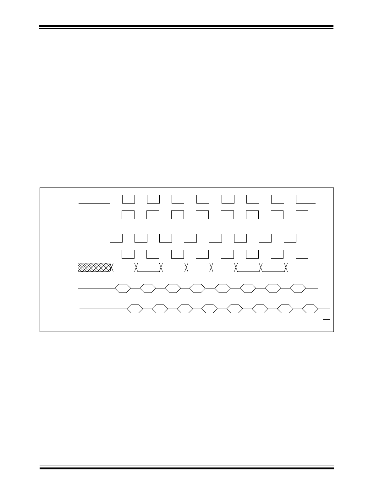
PIC16F872
9.1.1 MASTER MODE The master can initiate the data transfer at any time
because it controls the SCK. The master determines
when the slave (Processor 2, Figure 9-5) is to broadcast data by the software protocol.
In Master mode, the data is transmitted/received as
soon as the SSPBUF register is written to. If the SPI
module is only going to receive, the SDO output could
be disabled (programmed as an input). The SSPSR
register will co ntinue to s hift in the si gnal present o n the
SDI pin at the programmed clock rate. As each byte is
received, it will be loaded into the SSPBUF register as
if a normal received byte (interrupts and status bits
appropriately set). This could be useful in receiver
applications as a “line activity monitor”.
The clock polari ty is selected b y appropriately pr ogram-
ming bit CKP (SSPCON<4>). This then would give
waveforms for SPI communication as shown in
FIGURE 9-2: SPI MODE TIMING, MASTER MODE
SCK (CKP = 0,
CKE = 0)
SCK (CKP = 0,
CKE = 1)
SCK (CKP = 1,
CKE = 0)
SCK (CKP = 1,
CKE = 1)
Figure 9-6, Figure 9-8 and Figure 9-9 where the MSb is
transmitted first . In Master mode, the SPI cloc k rate (bit
rate) is user programmable to be one of the following:
OSC/4 (or TCY)
•F
•F
OSC/16 (or 4 • TCY)
•FOSC/64 (or 16 • TCY)
• Timer2 output/2
This allows a maxim um bit cloc k frequen cy (at 20 MHz)
of 5.0 MHz.
Figure 9-6 shows the waveforms for Master mode.
When CKE = 1, the SDO data is valid before there is a
clock edge on SCK. The change of the input sample is
shown based on the state of the SMP bit. The time
when the SSPBUF is loaded with the received data is
shown.
SDO
SDI (SMP = 0)
SDI (SMP = 1)
SSPIF
bit7
bit7
bit7 bit0
bit6 bit5
bit4
bit3
bit2
bit1 bit0
bit0
DS30221A-page 58 Preliminary
1999 Microchip Technology Inc.
Page 59
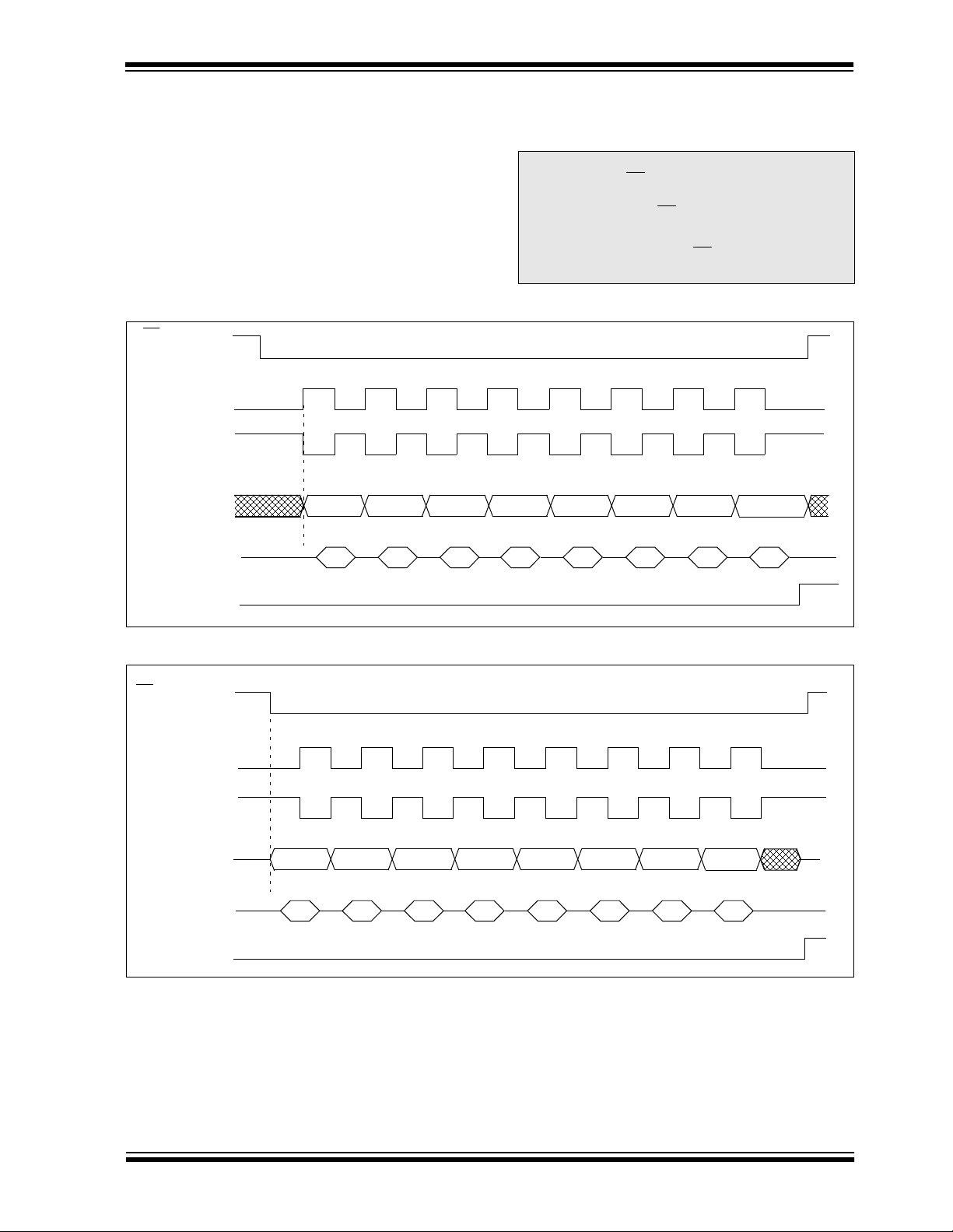
PIC16F872
9.1.2 SLAVE MODE
While in SLEEP mode, the slave can transmit/receive
data. When a byte is received, the device will wake-up
In Slave mode, the data is transmitted and received as
the external clock pulses appear on SCK. When the
last bit is latched, the interrupt fla g bit SSPIF (PIR1<3>)
is set.
While in Slave mode, the external clock is supplied by
the external cloc k sou rce o n the SCK p in. Th is external
clock must meet th e minimum high and low times as
specified in the electrical specifications.
from sleep.
Note: When the SPI module is in Slave mode
with SS
CON<3:0> = 0100) the SPI module will
reset if the SS pin is set to VDD.
Note: If the SPI is used in Slave mode with
CKE = ’1’, then SS
enabled.
FIGURE 9-3: SPI MODE TIMING (SLAVE MODE WITH CKE = 0)
SS (optional)
SCK (CKP = 0)
SCK (CKP = 1)
SDO
SDI (SMP = 0)
bit7
bit6 bit5
bit4
bit3
pin control enabled, (SSP-
pin control must be
bit2
bit1 bit0
bit7 bit0
SSPIF
FIGURE 9-4: SPI MODE TIMING (SLAVE MODE WITH CKE = 1)
SS
SCK (CKP = 0)
SCK (CKP = 1)
SDO
SDI (SMP = 0)
SSPIF
bit7
bit7 bit0
bit6 bit5
bit4
bit3
bit2
bit1 bit0
1999 Microchip Technology Inc.
Preliminary DS30221A-page 59
Page 60

PIC16F872
TABLE 9-1 REGISTERS ASSOCIATED WITH SPI OPERATION
Address Name Bit 7 Bit 6 Bit 5 Bit 4 Bit 3 Bit 2 Bit 1 Bit 0 POR, BOR
0Bh, 8Bh,
10Bh,18Bh
0Ch PIR1
8Ch PIE1
13h SSPBUF Synchronous Serial Port Receive Buffer/Transmit Register xxxx xxxx uuuu uuuu
14h SSPCON WCOL SSPOV SSPEN CKP SSPM3 SSPM2 SSPM1 SSPM0 0000 0000 0000 0000
94h SSPSTAT SMP CKE
INTCON GIE PEIE
(1)
PSPIF
PSPIE
ADIF RCIF TXIF SSPIF CCP1IF TMR2IF TMR1IF 0000 0000 0000 0000
(1)
ADIE RCIE TXIE SSPIE CCP1IE TMR2IE TMR1IE 0000 0000 0000 0000
T0IE INTE RBIE T0IF INTF RBIF 0000 000x 0000 000u
D/A P S R/W UA BF 0000 0000 0000 0000
Legend: x = unknown, u = unchanged, - = unimplemented read as ’0’. Shaded cells are not used by the SSP in SPI mode.
Note 1: These bits are reserved on the 28-pin devices; always maintain these bits clear.
MCLR
WDT
,
DS30221A-page 60 Preliminary
1999 Microchip Technology Inc.
Page 61

PIC16F872
9.2 MSSP I2 C Operation
The MSSP module in I2C mode fully implements all
master and slave functions (including general call support) and provides interrupts-on-start and stop bits in
hardware to determine a free bus (multi-master function). The MSSP module implements the standard
mode specifications, as well as 7-bit and 10-bit
addressing.
Refer to Application Note AN578,
Module in the I
2
C Multi-Master Environment."
"Use of the SSP
A "glitch" filter is on the SCL and SDA pins whe n the pin
is an input. This filter operates in b oth the 10 0 k Hz an d
400 kHz modes. In the 10 0 kHz mode, w hen these pins
are an output, there is a sle w ra te control of the pin that
is independent of device frequency.
FIGURE 9-5: I2C SLAVE MODE BLOCK
DIAGRAM
Internal
Data Bus
Read Write
SCL
Shift
Clock
SDA
SSPBUF reg
MSb
Match detect
SSPSR reg
LSb
Addr Match
Two pins are used for dat a t r a ns fer . The se ar e t he SCL
pin, which is the clock, and the SDA pin, which is the
data. The SDA and SCL pins are automatically configured when the I
2
C mode is enabled. The SSP module
functions are enabled by setting SSP Enable bit
SSPEN (SSPCON<5>).
2
The MSSP module has six registers for I
C operation.
They are the:
• SSP Control Register (SSPCON)
• SSP Control Register2 (SSPCON2)
• SSP Status Register (SSPSTAT)
• Serial Receive/Transmit Buffer (SSPBUF)
• SSP Shift Register (SSPSR) - Not directly
accessible
• SSP Address Register (SSPADD)
2
The SSPCON register allows control of the I
tion. Four mode selection bits (SSPCON<3:0>) allow
one of the following I
2
C Slave mode (7-bit address)
•I
2
•I
C Slave mode (10-bit address)
2
C Master mode, clock = OSC/4 (SSPADD +1)
•I
Before selecting any I
2
C modes to be sele cted:
2
C mode, the SCL and SDA pins
C opera-
must be programmed to inputs by setting the appropriate TRIS bits. Selecting an I2C mode, by setting the
SSPEN bit, enables the SCL and SDA pins to be used
as the clock and data lines in I
2
C mode.
The CKE bit (SSPSTAT<6:7>) sets the levels of the
SDA and SCL pins in either Master or Slave mode.
When CKE = 1, the levels will conform to the SMBUS
specification. Whe n CKE = 0, the le ve ls will c onf orm to
2
C specification.
the I
SSPADD reg
Start and
Stop bit detect
Set, Reset
S, P bits
(SSPSTAT reg)
1999 Microchip Technology Inc.
Preliminary DS30221A-page 61
Page 62

PIC16F872
The SSPSTAT register gives the status of the data
transfer. This information includes detection of a
START (S) or STOP (P) bit, specifies if the received
byte was data or ad dress, if the ne xt b yte is the com pletion of 10-bit address, and if this will be a read or write
data transfe r.
SSPBUF is the register to which the transfer data is
written to or read from. The SSPSR register shifts the
data in or out of the device. In receive operations, the
SSPBUF and SSPSR create a doubled buffered
receiver. This allows reception of the ne x t b yte to b egin
before reading the last byte of received data. When the
complete byte is received, it is transferred to the
SSPBUF register and flag bit SSPIF is set. If another
complete byte is received before the SSPBUF register
is read, a receiver overflow has occurred and bit
SSPOV (SSPCON<6>) is set and the byte in the
SSPSR is lost.
The SSPADD register holds the sla ve address. I n 10-bit
mode, the user needs to write the high byte of the
address (1111 0 A9 A8 0). Following the high byte
address match, the low byte of the address needs to be
loaded (A7:A0).
9.2.1 SLAVE MODE In Slave mode, the SCL and SDA pins must be config-
ured as inputs. The MSSP module will override the
input state with the output data when required (slavetransmitter).
When an address is matched or the data transfer after
an address match is received, the hardware automatically will generate the acknowledge (ACK
then load the SSPBUF register with the received value
currently in the SSPSR register.
There are certain conditions that will cause the MSSP
module not to give this ACK
(or both):
a) The buffer full bit BF (SSPSTAT<0>) was set
before the transfer was received.
b) The overflow bit SSPO V (SSPCON<6>) w as set
before the transfer was received.
If the BF bit is set, the SSPSR register value is not
loaded into the SSPBUF, but bit SSPIF and SSPOV are
set. Table 9-2 shows what happens when a data transfer byte is received, given the status of bits BF and
SSPOV. The shaded cells show the condition where
user software did not pro perly clea r the o v erfl ow c ondition. Flag bit B F is cleare d b y reading th e SSPBUF re gister, while bit SSPOV is cleared through software.
The SCL clock input must have a minimum high and
low time for proper operation. The high and low times
2
of the I
the MSSP module, is shown in timing parameter #100
and parameter #101 of the electrical specifications.
C specification, as well as the requirement of
pulse. These are if either
) pulse, and
9.2.1.1 ADDRESSING
Once the MSSP module has been enabled, it waits for
a START condition to occur. Following the START condition, the 8-bits are shifted in to the SSPSR register . All
incoming bits are sampled with the rising edge of the
clock (SCL) line. The value of register SSPSR<7:1> is
compared to the value of the SSPADD register. The
address is compared on the falling edge of the eighth
clock (SCL) pulse. If the addresses match, and the BF
and SSPOV bits are clear, the following events occur:
a) The SSPSR register value is loaded into the
SSPBUF register on the falling edge of the 8th
SCL pulse.
b) The buffer fu ll bit, BF, is set on the fal ling edg e of
the 8th SCL pulse.
c) An ACK
d) SSP interrupt flag bit, SSPIF (PIR1<3>), is set
(interrupt is generated if enabled) on the falling
edge of the 9th SCL pulse.
In 10-bit address mode, two address bytes need to be
received by the slave. The five Most Significant bits
(MSbs) of the first address b yte sp ecify if this is a 1 0-bit
address. Bit R/W
so the slave device will receive the second address
byte. For a 10-bit address, the first byte would equal
‘1111 0 A9 A8 0’, where A9 and A8 are the two MSbs
of the address. The sequence of events for a 10-bit
address is as follows, with steps 7- 9 for slavetransmitter:
1. Receive first (high) byte of Address (bits SSPIF,
BF and UA (SSPSTAT<1>) are set).
2. Update the SSPADD register with the second
(low) byte of Address (clears bit UA and
releases the SCL line).
3. Read the SSPBUF register (clears bit BF) and
clear flag bit SSPIF.
4. Receive second (low) byte of Address (bits
SSPIF, BF and UA are set).
5. Upd ate the SSPADD register with the fir st (hig h)
byte of Address. This will clear bit UA and
release the SCL line.
6. Read the SSPBUF register (clears bit BF) and
clear flag bit SSPIF.
7. Receive Repeated Start condition.
8. Receive first (high) byte of Address (bits SSPIF
and BF are set).
9. Read the SSPBUF register (clears bit BF) and
clear flag bit SSPIF.
Note: Following the Repeated Start condition
pulse is generated.
(SSPSTAT<2>) must specify a write
(step 7) in 10-bit mode, the user only
needs to match the first 7-bit addre ss. Th e
user does not update the SSPADD for the
second half of the address.
DS30221A-page 62 Preliminary
1999 Microchip Technology Inc.
Page 63
PIC16F872
9.2.1.2 SLAVE RE CEPTION
An SSP interrupt is generated for each data transfer
byte. Flag b it SSPIF (PIR1<3 >) must be cleared in soft-
When the R/W bit of the address byte is clear and an
address match occurs, the R/W
bit of the SSPSTAT
ware. The SSPSTAT register is used to determine the
status of the received byte.
register is cleared. The rece iv ed ad dress i s loade d into
the SSPBUF register.
When the address byte overflow condition exists, then
no acknowled ge (ACK
) pulse is given. An overflow condition is defined as either bit BF (SSPSTAT<0>) is set
or bit SSPOV (SSPCON<6>) is set.
Note: The SSPBUF will be loaded if the SSPOV
bit is set and the BF flag is cleared. If a
read of the SSPBUF was performed, but
the user did not clear the state of the
SSPOV bit before the next receive
occurred, the ACK
is not sent and the SSP-
BUF is updated.
TABLE 9-2 DATA T RANSFER RECEIVED BYTE ACTIONS
Status Bits as Data
Transfer is Received
Generate ACK
BF SSPOV
SSPSR
→ SSPBUF
Pulse
00 Yes Yes Yes
10 No No Yes
11 No No Yes
0 1 Yes No Yes
Note 1: Shaded cells show the conditions where the user software did not properly clear the overflow condition.
Set bit SSPIF
(SSP Interrupt occurs
if enabled)
9.2.1.3 SLAVE TRANSMISSION
An SSP interrupt is generated for each data transfer
byte. The SSPIF flag bit must be cleared in software
When the R/W bit of the incoming address byte is set
and an address match occurs, the R/W
bit of the
SSPSTAT register is set. The received address is
loaded into the SSPBUF register. The ACK
pulse will
be sent on the ninth bit, and the SCL pin is held low.
The transmit data must be loaded into the SSPBUF
register , which also loads the SSPSR register . Then the
SCL pin should be enabled by setting bit CKP (SSPCON<4>). The master must monitor the SCL pin prior
to asserting another clock pulse. The slave devices
may be holding off the master by stretchi ng the cl ock.
The eight data bits are shifte d out on the f alling edg e of
the SCL input. This ensures that the SDA signal is valid
during the SCL high time (Figure 9-7).
and the SSPSTA T register is used to determine the status of the byte tr an sfer. The SSPIF flag bit is set o n th e
falling edge of the ninth clock pulse.
As a slave-transmitter, the ACK
receiver is latched on the rising edge of the ninth SCL
input pulse. If the SDA line is high (not ACK), then the
data transfer is comple te . When the not ACK
by the slave, the slave logic is reset and the slave then
monitors for anoth er occurrence of the START bit. If the
SDA line was low (ACK
loaded into the SSPBUF register, which also loads the
SSPSR register. Then the SCL pin should be enabled
by setting the CKP bit.
FIGURE 9-6: I2C WAVEFORMS FOR RECEPTION (7-BIT ADDRESS)
Receiving Address
A7 A6 A5 A4
1234
S
SCL
SSPIF
BF (SSPSTAT<0>)
SSPOV (SSPCON<6>)
A3 A2 A1SDA
5
R/W=0
ACK
7
6
9
8
Receiving Data
D5
D6D7
1234
Cleared in software
SSPBUF register is read
Bit SSPOV is set because the SSPBUF register is still full.
D2
D3D4
56
D1
7
ACK
D0
89
Receiving Data
D5
D6D7
123
pulse from the master
is latched
), the transmit data must be
Not
ACK
D0
D2
D3D4
D1
9
5
4
ACK is not sent.
8
7
6
P
Bus Master
terminates
transfer
1999 Microchip Technology Inc.
Preliminary DS30221A-page 63
Page 64
PIC16F872
FIGURE 9-7: I2C WAVEFORMS FOR TRANSMISSION (7-BIT ADDRESS)
R/W
SDA
Receiving Address
A7 A6 A5 A4 A3 A2 A1
= 1
ACK
D7 D6 D5 D4 D3 D2 D1 D0
Transmitting Data
R/W
= 0
Not ACK
SCL
SSPIF
BF (SSPSTAT<0>)
CKP (SSPCON<4>)
123456789 123456789
S
Data in
sampled
9.2.2 GENERAL CALL ADDRESS SUPPORT
2
The addressing procedure for the I
C bus is such that
the first byte after the START condition usually determines which device will be the slave addressed by the
master. The exception is the general call address,
which can address all devices. When this address is
used, all devices should, in theory, respond with an
acknowledge.
The general call address is one of eight addresses
reserved for specific purposes by the I
consists of all 0’s with R/W
= 0
2
C protocol. It
The general call address is recognized when the General Call Enable bit (GCEN) is enable d (SSPCON2< 7>
is set). Following a start-bit detect, 8 bits are shifted
into SSPSR and the address is compared against
SSPADD. It is also compared to the general call
address and fixed in hardware.
SCL held low
while CPU
responds to SSPIF
If the general call address matches, the SSPSR is
transferred to the SSPBUF, the BF flag is set (eighth
bit), and on the f alling edg e of the ninth bi t (ACK
SSPIF flag is set.
When the interrupt is se rviced, the source for the interrupt can be checked by reading the contents of the
SSPBUF to determine if the address was device specific or a general call address.
In 10-bit mode, the SSPADD is required to be updated
for the seco nd half of th e address to match, and th e U A
bit is set (SSPSTAT<1>). If the general call address is
sampled when GCEN is set while the slave is configured in 10-bit address mode, then the second half of
the address is not ne cessary, the UA bit will no t be se t,
and the slave will begin receiving data after the
acknowledge (Figure 9-8).
cleared in software
SSPBUF is written in software
Set bit after writing to SSPBUF
(the SSPBUF must be written-to
before the CKP bit can be set)
From SSP interrupt
service routine
P
bit), the
FIGURE 9-8: SLAVE MODE GENERAL CALL ADDRESS SEQUENCE (7 OR 10-BIT MODE)
Address is compared to General Call Address
after ACK, set interrupt flag
R/W
SDA
SCL
S
SSPIF
BF
(SSPSTAT<0>)
SSPOV
(SSPCON<6>)
GCEN
(SSPCON2<7>)
DS30221A-page 64 Preliminary
General Call Address
123456789123456789
= 0
ACK
D7 D6 D5 D4 D3 D2 D1 D0
Receiving data
Cleared in software
SSPBUF is read
1999 Microchip Technology Inc.
ACK
’0’
’1’
Page 65

PIC16F872
9.2.3 SLEEP OPERATION While in SLEEP mode, the I2C module can receive
addresses or data. When an address match or com-
9.2.4 EFFECTS OF A RESET A RESET disables the SSP module and te rminates the
current transfer.
plete byte transfer occurs, wake the processor from
sleep (if the SSP interrupt is enabled).
TABLE 9-3 REGISTERS ASSOCIATED WITH I2C OPERATION
Address N ame Bit 7 Bit 6 B it 5 Bit 4 Bit 3 Bit 2 Bit 1 Bit 0 POR, BOR
0Bh, 8Bh,
10Bh,18Bh
0Ch PIR1
8Ch PIE1
0Dh PIR2
8Dh PIE2
13h SSPBUF Synchronous Serial Port Receive Buffer/Transmit Register xxxx xxxx uuuu uuuu
14h SSPCON WCOL SSPOV SSPEN CKP SSPM3 SSPM2 SSPM1 SSPM0 0000 0000 0000 0000
91h SSPCON2 GCEN ACKSTAT ACKDT ACKEN RCEN PEN RSEN SEN 0000 0000 0000 0000
94h SSPSTAT SMP CKE D/A
Legend: x = unknown, u = unchanged, r= reserved, - = unimplemented read as ’0’. Shaded cells are not used by the SSP in I2C
Note 1: These bits are reserved; always maintain these bits clear.
INTCON GIE PEIE
(1) ADIF (1) (1) SSPIF CCP1IF TMR2IF TMR1IF r0rr 0000 r0rr 0000
(1) ADIE (1) (1) SSPIE CCP1IE TMR2IE TMR1IE r0rr 0000 r0rr 0000
— (1) — EEIF BCL IF — — (1) -r-0 0--r -r-0 0--r
— (1) — EEIE BCLIE — — (1) -r-0 0--r -r-0 0--r
mode.
T0IE INTE RBIE T0IF INTF RBIF 0000 000x 0000 000u
PSR/WUA BF 0000 0000 0000 0000
MCLR
WDT
,
1999 Microchip Technology Inc.
Preliminary DS30221A-page 65
Page 66
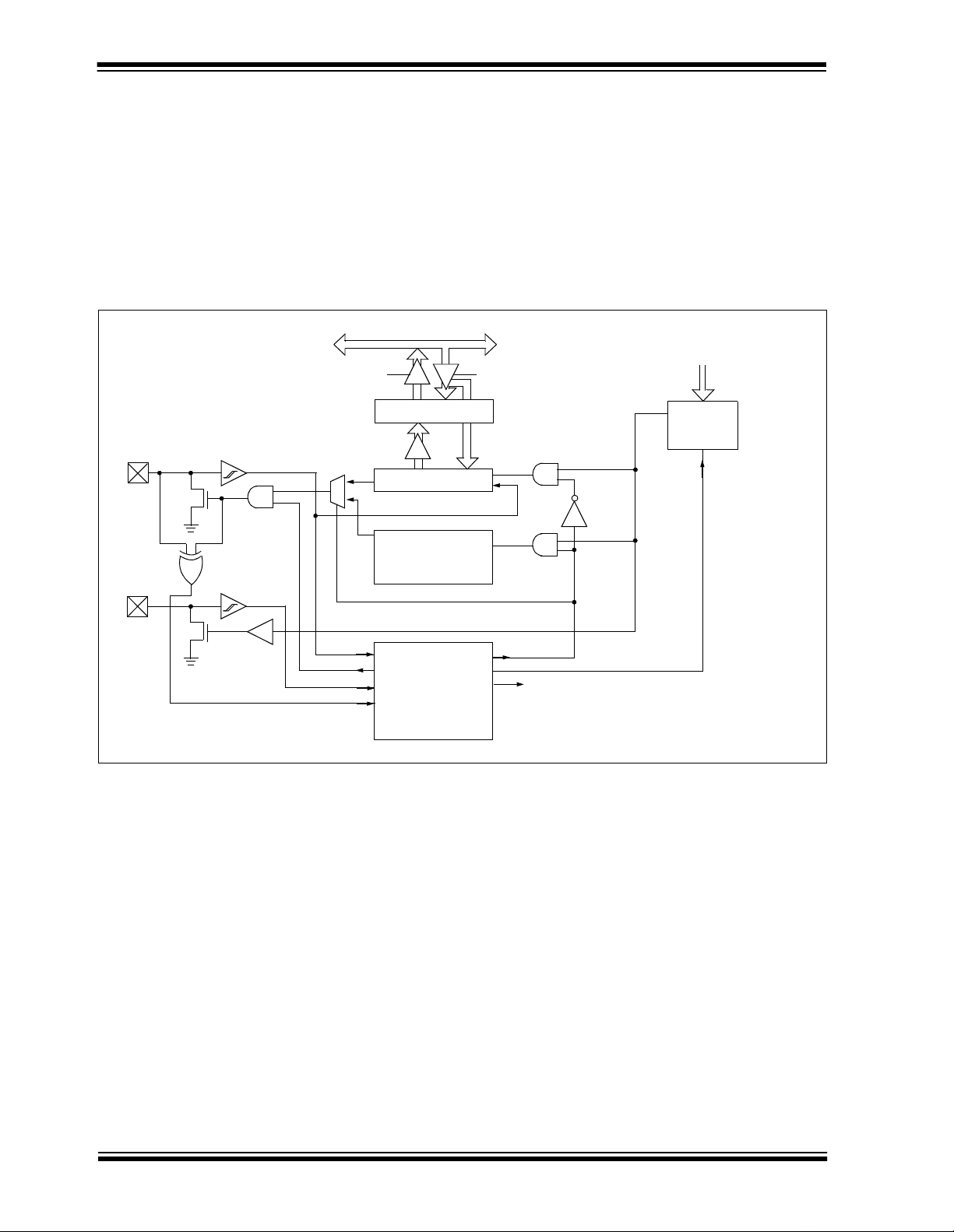
PIC16F872
9.2.5 MASTER MODE Master mode of operation is supported by interrupt
generation on the detection of the START and STOP
conditions. The STOP (P) and START (S) bits are
cleared from a RESET or when the MSSP module is
disabled. Control of the I
2
C bus may be TACKEN when
the P bit is set, or the bus is idle with both the S and P
bits clear.
In Master mode, the SCL and SDA lines are manipulated by the MSSP hardware .
The following events will cause the SSP Interrupt Flag
bit, SSPIF, to be set (SSP Interrupt if enabled):
• START condition
• STOP condition
• Data transfer byte transmitted/received
• Acknowledge transmit
• Repeated Start
FIGURE 9-9: SS P BLOCK DIAGRAM (I2C MASTER MODE)
Internal
Data Bus
Read Write
SSPBUF
LSb
Shift
Clock
SDA
SCL
SDA in
SSPSR
MSb
Start bit, Stop bit,
Acknowledge
Generate
Receive Enable
SSPM<3:0>,
SSPADD<6:0>
Baud
Rate
Generator
clock cntl
(hold off clock source)
clock arbitrate/WCOL detect
SCL in
Bus Collision
Start bit detect,
Stop bit detect
Write collision detect
Clock Arbitration
State counter for
end of XMIT/RCV
Set/Reset, S, P, WCOL (SSPSTAT)
Set SSPIF, BCLIF
Reset ACKSTAT, PEN (SSPCON2)
DS30221A-page 66 Preliminary
1999 Microchip Technology Inc.
Page 67

PIC16F872
9.2.6 MULTI-MASTER MODE In Multi-Master mode, the interrupt generation on the
detection of the START and STOP conditions allows
the determination of when the bus is free. The STOP
(P) and START (S) bits are cleared from a RESET or
when the MSSP module is disabled. Cont rol of th e I2C
bus may be TACKEN when bit P (SSPSTAT<4>) is set,
or the bus is idle with bot h the S and P bits clear. When
the bus is busy, enabling the SSP Interrupt will generate the interrupt when the STOP condition occurs.
In multi-master operation, the SDA line must be monitored for arbitration to see if the signal level is the
expected ou tpu t l evel. Th is c he ck is perf o rmed in ha rdware, with the result placed in the BCLIF bit.
The states where arbitration can be lost are:
• Address Transfer
• Data Transfer
• A Start Condition
• A Repeated Start Condition
• An Acknowledge Condition
2
9.2.7 I
Master mode is enabled by setting and clearing the
appropriate SSPM bits in SSPCON and by setting the
SSPEN bit. Once Master mode is enabled, the user
has six options.
Note: The MSSP Module , when c onfigured in I2C
C MASTER MODE SUPPORT
- Assert a start condition on SDA and SCL.
- Assert a Repeated Start condition on SDA and
SCL.
- Write to the SSPBUF register initiating transmission of data/address.
- Generate a stop condition on SDA and SCL.
- Configure the I
- Generate an Acknow ledg e con dition at the end
of a received byte of data.
Master mode, does not allow queueing of
events. For instance, the user is not
allowed to initiate a start condition and
immediately write the SSPBUF register to
initiate transmission before the START
condition is complete. In this case, the
SSPBUF will not be written to and the
WCOL bit will be s et, in dicat ing t hat a wri te
to the SSPBUF did not occur.
2
C port to receive data.
2
9.2.7.4 I
The master device generates all of the serial clock
pulses and the START and STOP condition s . A transfer is ended with a STOP condition or with a Repeated
Start condition. Since the Repeated Start condition is
also the beginning of the next serial transfer, the I2C
bus will not be released.
In Master Transmitter mode, serial data is output
through SDA, while SCL outputs the serial clock. The
first byte transmitted contains the slave address of the
receiving device (7 bits) and the Read/Write (R/W
In this case, the R/W
transmitted 8 bits at a time. After each byte is transmitted, an acknow le dg e bit is recei ved. START and STOP
conditions are output to indicate the beginning and the
end of a serial transfer.
In Master Receive mode, the first b yte trans mitted contains the slave address of the transmitting device
(7 bits) and the R/W
logic '1'. Thus, the first byte transmitted is a 7-bit slave
address followed by a '1' to indicate receive bit. Serial
data is received via SDA, while SCL outputs the serial
clock. Serial data is receiv ed 8 bits at a time . After each
byte is received, an acknowledge bit is transmitted.
START and STOP conditions indicate the beginning
and end of transmission.
The baud rate generator used for SPI mode operation
is now used to set the SCL clock frequency for either
100 kHz, 400 kHz or 1 MHz I
rate generator reload value is contained in the lower 7
bits of the SSPADD register. The baud rate generator
will automatically begin counting on a write to the
SSPBUF. Once the given operation is complete (i.e.,
transmission of the last data b it is f ollow ed by A CK), the
internal clock will automatically stop counting and the
SCL pin will remain in its last state
A typical transmit sequence would go as follows:
a) The user generates a Start Condition by setting
the START enable bit (SEN) in SSPCON2.
b) SSPIF is set. The module will wait the required
start time before any other operation takes
place.
c) The user loads the SSPBUF with address to
transmit.
d) Address is shifted out th e SDA pin until all 8 bits
are transmitted.
e) The MSSP Module shifts in the ACK bit from the
slave device and writes its value into the
SSPCON2 register ( SSPCON2<6>).
f) The module generates an interrupt at the en d of
the ninth clock cycle by setting SSPIF.
g) The user loads the SSPBUF with eight bits of
data.
h) DATA is shifted out the SDA pin until all 8 bits
are transmitted.
C MASTER MODE OPERATION
bit will be logic '0'. Serial data is
bit. In this case , the R/W bit wil l be
2
C operation. The baud
) bit.
1999 Microchip Technology Inc.
Preliminary DS30221A-page 67
Page 68

PIC16F872
i) The MSSP module shifts in the A CK bit from the
slave device, and writes its value into the
SSPCON2 register ( SSPCON2<6>).
j) The MSSP module generates an int errupt at the
In I2C Master mode, the BRG is rel oaded automa tically.
If Clock Arbitration is taking place for instance, the BRG
will be reloaded when the SCL pin is sampled high
(Figure 9-11).
end of the ninth cloc k cycle b y set ting the SSPIF
bit.
k) Th e user gene rates a ST OP condition by settin g
the STOP enable bit PEN in SSPCON2.
l) Interrupt is generated once the STOP condition
FIGURE 9-10: BAUD RATE GENERATOR
BLOCK DIAGRAM
SSPM<3:0>
SSPADD<6:0>
is complete.
9.2.8 BAUD RATE GENERATOR
2
C Master mode, the reload value for the BRG is
In I
SSPM<3:0>
SCL
Reload
Control
Reload
located in the lower 7 bits of the SSPADD register
(Figure 9-10). When the BRG is loaded with this v alue ,
CLKOUT
BRG Down Counter
the BRG counts down to 0 and stops until another
reload has TACKEN place. Th e BRG count is decre mented twice per instruction c ycle (T
CY), on the Q2 and
Q4 clock.
FIGURE 9-11: BAUD RATE GENERATOR TIMING WITH CLOCK ARBITRATION
SDA
SCL deasserted but slave holds
SCL low (clock arbitration)
SCL
DX-1DX
SCL allowed to transition high
F
OSC/4
BRG
value
BRG
reload
BRG decrements
(on Q2 and Q4 cycles)
03h 02h 01h 00h (hold off) 03h 02h
SCL is sampled high, reload takes
place, and BRG starts its count.
DS30221A-page 68 Preliminary
1999 Microchip Technology Inc.
Page 69

PIC16F872
9.2.9 I2C MASTER MODE START CONDITION TIMING
To initiate a START condition, the user sets the start
condition enable bit, SEN (SSPCON2<0>). If the SDA
and SCL pins are sampled hi gh, the baud rate gener ator is re-loaded with th e content s of SSPADD<6:0> and
starts its count. If SCL and SDA are bo th sample d high
when the baud rate generator times out (T
BRG), the
SDA pin is driven low. The action of the SDA being
driven low whil e SCL is high i s the START condition,
and causes the S bit (SSPSTAT<3>) to be set. Following this, the baud rate generator is reloaded with the
contents of SSPADD<6:0> and resumes its count.
When the baud rate generator times out (T
BRG), the
SEN bit (SSPCON2<0>) will be automatically cleared
by hardware. The baud rate generator is suspended
leaving the SDA line held low, and the START condition
is complete.
FIGURE 9-12: FIRST START BIT TIMING
Write to SEN bit occurs here.
SDA = 1,
SCL = 1
TBRG
Note: If at the beginning of START condition the
SDA and SCL pins are already sampled
low, or if during the START condition the
SCL line is sampled low before the SDA
line is driven low , a b us collision occ urs, the
Bus Collision Interrupt Flag (BCLIF) is set,
the START condition is aborted, and the
2
C module is reset into its IDLE state.
I
9.2.9.5 WCOL STATUS FLAG
If the user writes the SSPBUF when an START
sequence is in progress, then WCOL is set and the
contents of the b uff er are u nchan ged (the w rite doesn ’t
occur).
Note: Because queueing of events is not
allowed, writing to the lower 5 bits of
SSPCON2 is disabled until the START
condition is complete.
Set S bit (SSPSTAT<3>)
At completion of start bit,
Hardware clears SEN bit
and sets SSPIF bit
TBRG
Write to SSPBUF occurs here
SDA
SCL
1st Bit
TBRG
TBRG
S
2nd Bit
1999 Microchip Technology Inc.
Preliminary DS30221A-page 69
Page 70

PIC16F872
9.2.10 I2C MASTER MODE REPEATED START CONDITION TIMING
A Repeated Start condition occurs when the RSEN bit
(SSPCON2<1>) is programmed high and the I
2
C module is in the idle state. When the RSEN bit is set, the
SCL pin is asserted low. When the SCL pin is sampled
low , the baud ra te genera tor is loaded with the contents
of SSPADD<6:0> and begins counting. The SD A pin i s
released (brought high) for one baud rate generator
count (T
BRG). When the baud rate generator times out
if SDA is sample d high, the SCL pin will be dea ss erted
(brought high). When SCL is sampled high the baud
rate generator is reloaded with the contents of
SSPADD<6:0> and begins counting. SDA and SCL
must be sampled high for one T
BRG. This action is then
followed by assertion of the SDA pin (SDA is low) for
one TBRG, while SCL is high. F ollow ing this, th e RSEN
bit in the SSPCON2 register will be automatically
cleared and the baud rate generator will not be
reloaded, l eaving th e SDA pin held low. As soon as a
start condition is detected on the SDA and SCL pins,
the S bit (SSPSTAT<3>) will be set. The SSPIF bit will
not be set until the baud rate generator has timed-out.
Note 1: If RSEN is programme d while any other
event is in progress, it will not take effect.
Note 2: A bus collision during the Repeated Start
condition occurs if:
• SDA is sampled low when SCL goes
from low to high.
• SCL goes low before SDA is asserted
low. This may indicate that another
master is attempting to transmit a
data "1".
Immediately following the SSPIF bit getting set, the
user may write the SSPBUF with the 7-bit address in
7-bit mode, or the default first address in 10-bit mode.
After the first eight bits are transmitted and an ACK is
received, the user may then transmit an additional eight
bits of address (10-bit mode) or eight bits of data (7-bit
mode).
9.2.10.6 WCOL STATUS FLAG
If the user writes the SSPBUF when a Repeated Start
sequence is in progress, then WCOL is set and the
contents of the b uff er are u nchan ged (the w rite doesn ’t
occur).
Note: Because queueing of events is not
allowed, writing of the lower 5 bits of
SSPCON2 is disabled until the Repeated
Start condition is complete.
FIGURE 9-13: REPEAT START CONDITION WAVEFORM
Write to SSPCON2
occurs here.
SDA = 1,
SCL(no change)
SDA
Falling edge of ninth clock
DS30221A-page 70 Preliminary
End of Xmit
SCL
SDA = 1,
SCL = 1
TBRG TBRG
Set S (SSPSTAT<3>)
At completion of start bit,
hardware clear RSEN bit
and set SSPIF
TBRG
Write to SSPBUF occurs here.
TBRG
Sr = Repeated Start
1st Bit
TBRG
1999 Microchip Technology Inc.
Page 71

PIC16F872
9.2.11 I2C MASTER MODE TRANSMISSION Transmission of a data byte, a 7-bit address or either
half of a 10-bit address , is accomp lished b y s imply writing a value to SSPBUF registe r . This action will set the
buffer fu ll flag (BF) and allo w the baud rate gener ator to
begin counting and start the next transmission. Each
bit of address/data will be shifted out onto the SDA pin
after the fall ing edg e of S CL is ass erted (see data hol d
time spec). SCL is held low for one baud rate generator rollover co unt (T
SCL is released high (see data setup time spec).
When the SCL pin is released high, it is held that way
BRG. The data on the SDA pin mus t rem ai n s ta b l e
for T
for that duration and some hold time after the next falling edge of SCL. After the eighth bit is shifted out (the
falling edge of the eighth clock), the BF flag is cleared
and the master r elease s SDA allo wing th e sla ve dev ice
being addressed to respo nd with an AC K
ninth bit time, if an a ddress m atch occu rs or i f data wa s
received prop erly. The status of ACK
ACKDT on the falling edge of the ninth clock. If the
master receives an acknowledge, the acknowledge
status bit (ACKSTAT) is cleared. If not, the bit is set.
After the ninth clock, the SSPIF is set and the master
clock (baud rate generator) is suspended until the next
data byte is loaded into the SSPBUF, leaving SCL low
and SDA unchanged (Figure 9-14).
After the write to the SSPBUF, each bit of address will
be shifted out on the falling edge of SCL until all seven
address bits and t he R/W
ing edge of the eighth clock, the master will de-assert
the SDA pin allowing the slave to respond with an
acknowle dge. O n the f all ing edge of the ninth cl ock, th e
master will sample the SDA pin to see if the address
was recogniz ed b y a sl ave. The status of the ACK bit is
loaded into the ACKSTAT status bit (SSPCON2<6>).
Following the falling edge of the ninth clock transmission of the address, the SSPIF is set, the BF flag is
cleared, and the baud rate generator is turned off until
another write to the SSPBUF takes place, holding SCL
low and allowing SDA to float.
BRG). Data should be valid before
bit during the
is read into the
bit are complet ed. On the fall-
9.2.11.9 ACKSTAT STATUS FLAG
In Transmit mode, the ACKSTAT bit (SSPCON2<6>) is
cleared when the slave has sent an acknowledge
= 0) and is set when the sla ve does not ac kno wl-
(ACK
edge (ACK
it has recognized its address (including a general call)
or when the slave has properly received its data.
= 1). A slave sends an acknowledge when
9.2.11.7 BF STATUS FLAG
In Transmit mode, the BF bit (SSPSTAT<0>) is set
when the CPU writes to SSPBUF and is cleared when
all 8 bits are shifted out.
9.2.11.8 WCOL STATUS FLAG
If the user writes the SSPBUF when a transmit is
already in progress (i.e., SSPSR is still shifting out a
data byte), then WCOL is set and the contents of the
buffer are unchanged (the write doesn’t occur).
WCOL must be cleared in software.
1999 Microchip Technology Inc.
Preliminary DS30221A-page 71
Page 72

PIC16F872
FIGURE 9-14: I2C MASTER MODE TIMING (TRANSMISSION, 7 OR 10-BIT ADDRESS)
P
ACKSTAT in
SSPCON2 = 1
ACK
Cleared in software
From slave clear ACKSTAT bit SSPCON2<6>
Write SSPCON2<0> SEN = 1
START c ondition begins
Transmitting Data or Second Half
of 10-bit address
= 0Transmit Address to Slave
R/W
SEN = 0
A7 A6 A5 A4 A3 A2 A1 ACK = 0 D7D6D5D4D3D2D1D0
Cleared in software service routine
From SSP interrupt
SCL held low
while CPU
responds to SSPIF
Cleared in software
123456789 123456789
start transmit
SSPBUF written with 7-bit address and R/W
S
SSPBUF is written in software
SSPBUF written
After start condition SEN cleared by hardware.
SDA
SCL
SSPIF
BF (SSPSTAT<0>)
SEN
PEN
DS30221A-page 72 Preliminary
R/W
1999 Microchip Technology Inc.
Page 73

9.2.12 I2C MASTER MODE RECEPTION Master mode rece pti on is enabled by prog r am m ing th e
receive enable bit, RCEN (SSPCON2<3>).
Note: The SSP module must be in an IDLE
STATE before the RCEN bit is set or the
RCEN bit will be disregarded.
The baud rate gen erator begins cou nting, and on each
rollover, the state of the SCL pin changes (high to
low/low to high), and data is shifted into the SSPSR.
After the falling edge of the eighth clock, the receive
enable flag is au tomatical ly cleare d, the contents of the
SSPSR are loaded into the SSPBUF, the BF flag is set,
the SSPIF is set, and the baud rate generator is suspended from counting, holding SCL low. The SSP is
now in IDLE state, awaiting the next command. When
the buffer is read by the CPU, the BF flag is automatically cleared. The user c an th en send an acknow l edg e
bit at the end of reception, by setting the acknowledge
sequence enable bit, ACKEN (SSPCON2<4>).
9.2.12.10 BF STATUS FLAG
PIC16F872
In receive operat ion, BF i s set w hen an address or data
byte is loaded into SSPBUF from SSPSR. It is cleared
when SSPBUF is read.
9.2.12.11 SSPOV STATUS FLAG
In receive operation, SSPOV is set when 8 bits are
received into the SSPSR and the BF flag is alrea dy set
from a previous recepti on.
9.2.12.12 WCOL STATU S FLAG
If the user writes the SSPBUF when a receive is
already in progress (i .e., SSPSR is still shifting i n a data
byte), then WCOL is set and the contents of the buffer
are unchanged (the write doesn’t occur).
1999 Microchip Technology Inc.
Preliminary DS30221A-page 73
Page 74
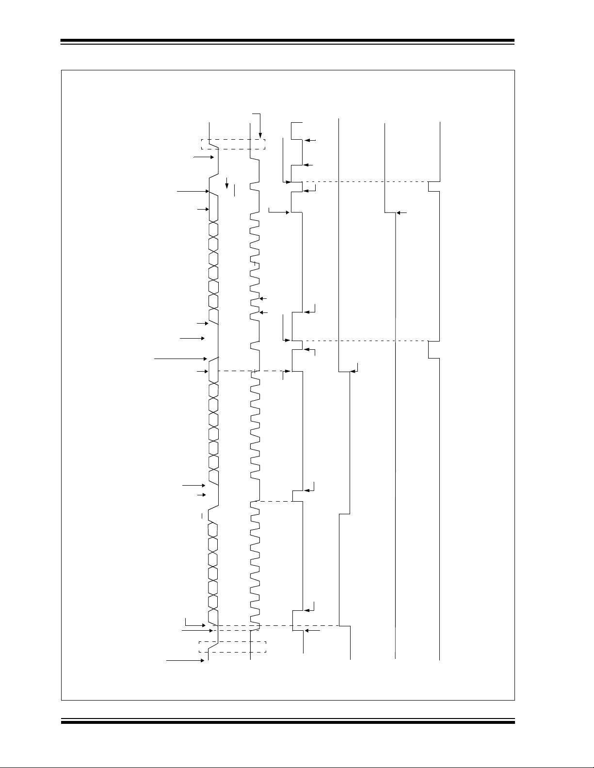
PIC16F872
FIGURE 9-15: I2C MASTER MODE TIMING (RECEPTION 7-BIT ADDRESS)
Bus Master
terminates
transfer
Set SSPIF interrupt
at end of acknow-
ledge sequence
Set P bit
(SSPSTAT<4>)
sequence
and SSPIF
Cleared in
software
SSPOV is set because
SSPBUF is still full
Cleared in software
Last bit is shifted into SSPSR and
contents are unloaded into SSPBUF
Write to SSPCON2<4>
to start acknowledge sequence
SDA = ACKDT (SSPCON2<5>) = 0
PEN bit = 1
SDA = ACKDT = 1
Set ACKEN start acknowledge sequence
ACK from Master
SDA = ACKDT = 0
RCEN cleared
RCEN = 1 start
written here
automatically
next receive
P
ACK is not sent
9
87
6
5
1234
of receive
Set SSPIF at end
Set SSPIF interrupt
at end of acknowledge
Data shifted in on falling edge of CLK
ACK
D0
D1
D2
D3D4
D5
D6D7
Receiving Data from Slave
ACK
D0
D1
RCEN cleared
automatically
D2
D3D4
D5
D6D7
Receiving Data from Slave
Master configured as a receiver
by programming SSPCON2<3>, (RCEN = 1)
SEN = 0
Write to SSPCON2<0> (SEN = 1)
Begin Start Condition
ACK
R/W = 1
ACK from Slave
A3 A2 A1
Transmit Address to Slave
Start XMIT
Write to SSPBUF occurs here
A7 A6 A5 A4
678 9
5
4
3
12
9
8
7
6
5
4
3
12
S
Cleared in softwar e
Set SSPIF interrupt
at end of receive
Cleared in software
Cleared in software
SDA
SCL
SSPIF
BF
(SSPSTAT<0>)
responds to SSPIF
while CPU
SDA = 0, SCL = 1
DS30221A-page 74 Preliminary
SSPOV
ACKEN
1999 Microchip Technology Inc.
Page 75
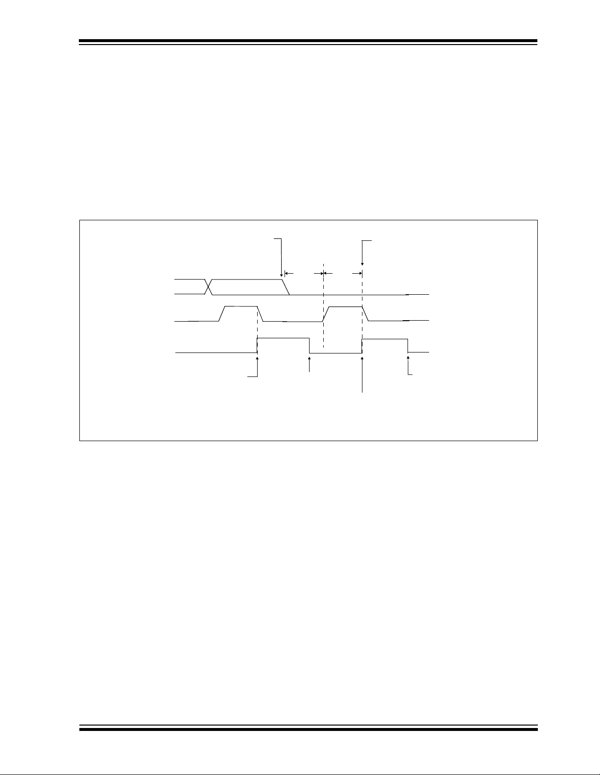
PIC16F872
9.2.13 ACKNOWLEDGE SEQUENCE TIMING
the baud rate generator counts for TBRG. The SCL pin
is then pulled low. Following this , the ACKEN bi t is auto-
An acknowledge sequence is enabled by setting the
acknowledge sequence enable bit, ACKEN
(SSPCON2<4>). When this bit is set, the SCL pin is
matically cleared, th e baud r ate gener ator is tu rned off ,
and the SSP module then goes into IDLE mode.
(Figure 9-16)
pulled low and the contents of the acknowledge data
bit is presented on the SDA pin. If the user wishes to
9.2.13.13 WCOL STATUS FLAG
generate an acknowledge, the ACKDT bit should be
cleared. If not, the user should set the ACKDT bit
before starting an acknowledge sequence. The baud
rate generator then counts for one rollover period
BRG), and the SCL pin is deasserted (pulled high).
(T
If the user writes the SSPBUF when an acknowledege
sequence is in p r og re ss, the WCOL is s et an d the con-
tents of the buffer are unchanged (the write doesn’t
occur).
When the SCL pin is sampled high (clock arbitration),
FIGURE 9-16: ACKNOWLEDGE SEQUENCE WAVEFORM
Acknowledge sequence starts here,
SDA
SCL
SSPIF
Write to SSPCON2
ACKEN = 1, AC KDT = 0
D0
8
TBRG
TBRG
ACK
9
ACKEN automatically cleared
Set SSPIF at the end
of receive
Note: TBRG = one baud rate generator period.
Cleared in
software
Cleared in
software
Set SSPIF at the end
of acknowledge sequence
1999 Microchip Technology Inc.
Preliminary DS30221A-page 75
Page 76

PIC16F872
9.2.14 STOP CONDITION TIMING A stop bit is asserted on the SDA pin at the end of a
receive/transmit by setting the Stop Sequence Enable
bit PEN (SSPCON2<2>). At the end of a receiv e/tr ansmit, the SCL line is held lo w afte r the falling edge of the
ninth clock. When the PEN bit is set, the master will
assert the SDA line low . When the SDA line is sampled low, the baud rate generator is reloaded and
counts down to 0 . Wh en th e bau d r ate g enera tor ti mes
out, the SCL pin will be brought high, and one T
BRG
(baud rate generator rollover count) later, the SDA pin
will be deasserted. When the SDA pin is sa mpled hig h
while SCL is high, the P bit (SSPSTAT<4>) is set. A
BRG later, the PEN bit is clea red an d th e SSPI F bi t is
T
set (Figure 9-17).
Whenever the firmware decides to take control of the
bus, it will firs t determine if the bus is b u sy by checking
the S and P bits in the SSPSTAT register. If the bus is
busy, then the CPU can be interrupted (notified) when
a Stop bit is detected (i.e., bus is free).
9.2.14.14 WCOL STATUS FLAG
If the user writes the SSPBUF when a ST OP sequence
is in progress , then WCOL is set and the con tents of the
buffer are unchanged (the write doesn’t occur).
FIGURE 9-17: STOP CONDITION RECEIVE OR TRANSMIT MODE
Write to SSPCON2
Falling edge of
9th clock
SCL
Set PEN
T
SCL = 1 for T
after SDA sampled high. P bit (SSPSTAT<4>) is set
BRG
BRG, followed by SDA = 1 for TBRG
PEN bit (SSPCON2<2>) is cleared by
hardware and the SSPIF bit is set
SDA
ACK
BRG
T
SDA asserted low before rising edge of clock
to setup stop condition.
Note: TBRG = one baud rate generator period.
P
T
BRG
SCL brought high after T
TBRG
BRG
DS30221A-page 76 Preliminary
1999 Microchip Technology Inc.
Page 77
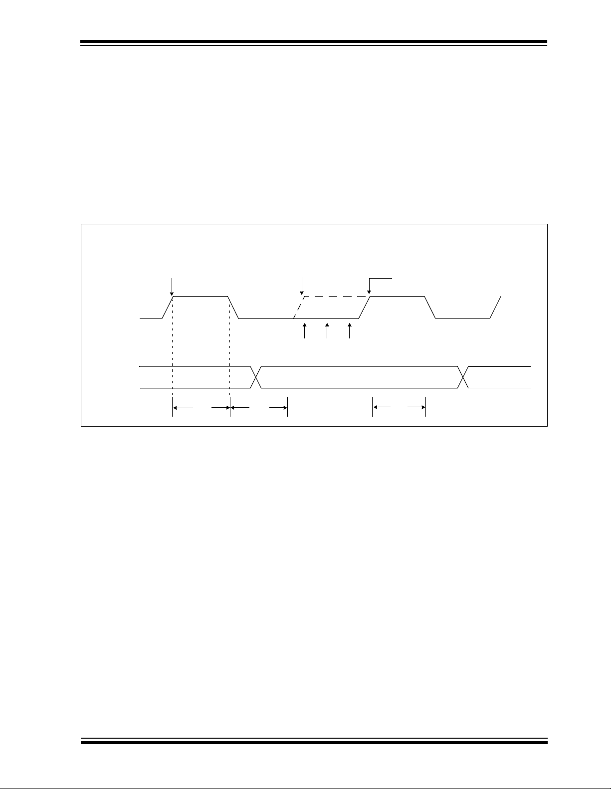
PIC16F872
9.2.15 CLOCK ARBITRATION Clock arbitration occurs when the master, during any
receive, transmit, or repeated start/stop condition,
deasserts the SCL pin (SCL allowed to float high).
When the SCL pin is allowed to flo at high, the baud rate
9.2.16 SLEEP OPERATION
While in SLEEP mode, the I
addresses or data, and when an address match or
complete byte transfe r occurs, wa ke the proc essor from
sleep (if the SSP interrupt is enabled).
generator (BRG) is suspended from counting until the
SCL pin is act ually sam pled high. Wh en the S CL pin is
sampled high, the baud rate gen erato r is reloade d with
the contents of SSPADD<6:0> and begins counting.
This ensures that the SCL high time will always be at
9.2.17 EFFECTS OF A RESET
A RESET disables the SSP module and te rminates the
current transfer.
least one BRG rollo v er cou nt in th e e v e nt that the c loc k
is held low by an external device (Figure 9-18).
FIGURE 9-18: CLOCK ARBITRATION TIMING IN MASTER TRANSMIT MODE
BRG overf l ow,
Release SCL,
If SCL = 1 Load BRG with
SSPADD<6:0>, and start count
to measure high time interval
SCL
BRG overf l ow occur s,
Release SCL, Slave device holds SCL low.
SCL line sampled once every machine cycle (T
Hold off BRG until SCL is sampled high.
SCL = 1 BRG starts counting
clock high interval.
2
C module can receive
OSC
4).
•
SDA
TBRG
TBRG
TBRG
1999 Microchip Technology Inc.
Preliminary DS30221A-page 77
Page 78
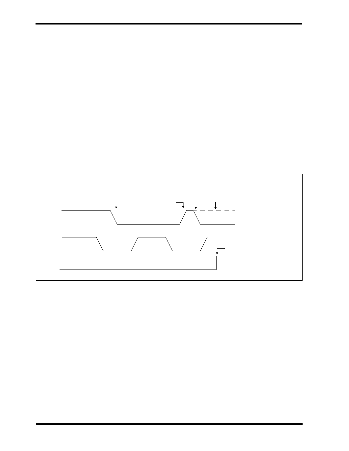
PIC16F872
9.2.18 MULTI -MASTER COMMUNICATION, BUS COLLISION, AND BUS ARBITRATION
If a START, Repeated Start, STOP or Acknowledge
condition was in progress when the bus collision
occurred, t he condition is abor ted, the SDA and SCL
Multi-Master mode support is achieved by bus arbitration. When the master outputs address/data bits onto
the SDA pin, arbitration takes place when the master
outputs a ’1’ on SDA by letting SDA float high and
another master as s erts a ’0’. Wh en the SC L pin fl oats
high, data should be stable. If the expected data on
SDA is a ’ 1’ and the data sa mpled on the SDA pin = ’0’,
a bus collis ion has take n place . The master w ill set the
Bus Collision Interrupt Flag, BCLIF, and reset the I
2
port to its IDLE st ate. (Figure 9-19).
If a transmit was in progress when the bus collision
occurred, the transmission is halted, the BF flag is
cleared, the SDA and SCL lines are deasserted, and
the SSPBUF can be written to . When the user services
the bus colli sion i nterrupt service rou tine , and if the I
2
bus is free, the user can resume communication by
asserting a START cond iti on.
C
C
lines are deasserted, and the respective control bits in
the SSPCON2 register are cleared. When the user
services the bus collision interrupt service routine, and
2
C bus is free, the user can resume communica-
if the I
tion by asserting a START condition.
The master will continue to monitor the SDA and SCL
pins, and if a ST OP co nditio n occurs , the S SPIF bit will
be set.
A write to the SSPBUF will start the transmission of
data at the first data bit, regardless of where the transmitter left off when the bus collision occurred.
In Multi-Master mode, the interrupt generation on the
detection of start and stop conditions allows the determination of when th e bus is free. Control of the I
can be taken when the P bit is set in the SSPSTAT register, or the bu s is idle a nd the S and P bits are cleared.
FIGURE 9-19: BUS COLLISION TIMING FOR TRANSMIT AND ACKNOWLEDGE
Data changes
while SCL = 0
SDA line pulled low
by another source
SDA re leased
by master
Sample SDA. While SCL is high,
data doesn’t match what is driven
by the master.
Bus collision has occurred.
2
C bus
SDA
SCL
BCLIF
Set bus collision
interrupt.
DS30221A-page 78 Preliminary
1999 Microchip Technology Inc.
Page 79
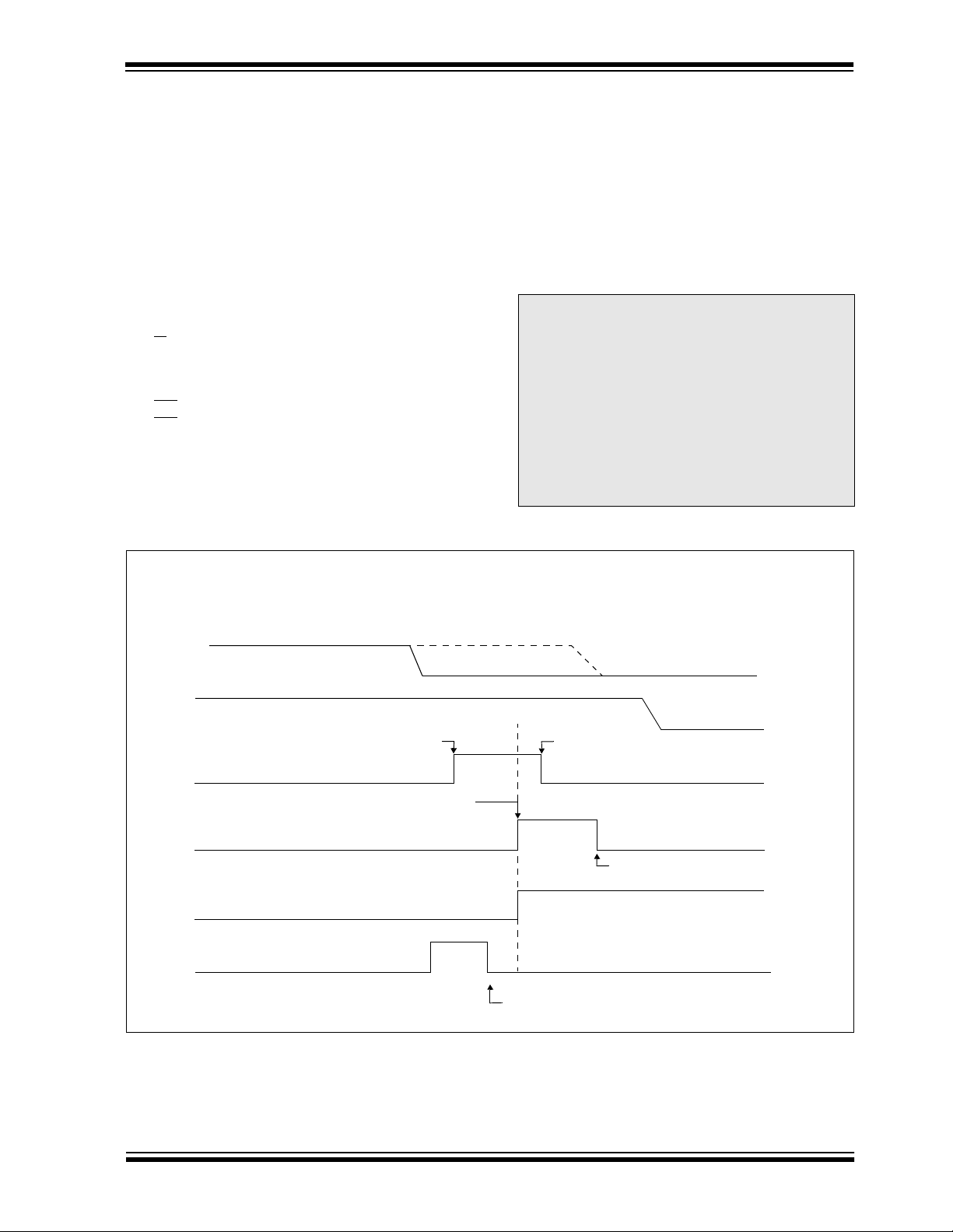
PIC16F872
9.2.18.15 BUS COLLISION DURING A START
CONDITION
During a START condition, a bus collision occurs if:
a) SDA or SCL are sampled low at the beginn ing of
the START condition (Figure 9-20).
b) SCL is sampled low before SDA is asserted low.
(Figure 9-21).
During a START condition both the SDA and the SCL
pins are monitored.
If:
the SDA pin is already low
the SCL pin is already low,
or
then:
the START condition is aborted,
the BCLIF flag is set,
and
the SSP module is reset to its IDLE state
and
(Figure 9-20).
The START condition begins with the SDA and SCL
pins deas ser t ed. When the S DA pin is s ample d high ,
the baud rate generator is loaded from SSPADD<6:0>
and counts down to 0. If the SCL pin is sampled low
while SDA is high, a bus collision occurs, because it is
assumed that another master is attempting to drive a
data ’1’ during the START condition.
If the SDA pin is sampled low during this count, the
BRG is reset and the SDA line is asserted early
(Figure 9-22). If, however, a ’1’ is sampled on the SDA
pin, the SDA pin is asserted low at the end of the BRG
count. The baud rate generator is then reloaded and
counts down to 0. During this time, if the SCL pins are
sampled as ’0’, a bus collision does not occur. At the
end of the BRG count, the SC L p in i s ass erted low.
Note: The reason that bus collision is not a f actor
during a START condition is that no two
bus masters can assert a ST ART condition
at the exact same time. Therefore, one
master will always assert SDA before the
other. T his cond ition d oes not ca use a b us
collision, becaus e the tw o masters must be
allowed to arb itrate the first addr ess f oll owing the START condition. If the address is
the same, arbitration must be allowed to
continue into the d ata p ortion, REPEATED
START or STOP conditions.
FIGURE 9-20: BUS COLLISION DURING START CONDITION (SDA ONLY)
SDA
SCL
SEN
BCLIF
S
SSPIF
SDA goes low before the SEN bit is set.
Set BCLIF,
S bit and SSPIF set because
SDA = 0, SCL = 1
Set SEN, enable start
condition if SDA = 1, SCL=1
SDA sampled low before
START condition.
S bit and SSPIF set because
SDA = 0, SC L = 1
Set BCLIF.
SEN cleared automatically because of bus collision.
SSP module reset into idle state.
SSPIF and BCLIF are
cleared in software.
SSPIF and BCLIF are
cleared in software.
1999 Microchip Technology Inc.
Preliminary DS30221A-page 79
Page 80

PIC16F872
FIGURE 9-21: BUS COLLISION DURING START CONDITION (SCL = 0)
SDA = 0, SCL = 1
TBRG
SCL = 0 before SDA = 0,
Bus collision occurs, Set BCLIF
Interru p ts c l e a re d
in software
’0’
’0’
SDA
SCL
SEN
BCLIF
S
SSPIF
Set SEN, enable start
sequence if SDA = 1, SCL = 1
SCL = 0 before BRG time out,
Bus collision occurs, Set BCLIF
’0’
’0’
TBRG
FIGURE 9-22: BRG RESET DUE TO SDA COLLISION DURING START CONDITION
SDA = 0, SCL = 1
Set SSPIF
Less than T
SDA pulled low by other master
SDA
Reset BRG and assert SDA
BRG
Set S
TBRG
SCL
SEN
BCLIF
S
SSPIF
s
SCL pulled low after BRG
Timeout
Set SEN, enable start
’0’
sequence if SDA = 1, SCL = 1
SDA = 0, SCL = 1
Set SSPIF
Interrupts cleared
in software
DS30221A-page 80 Preliminary
1999 Microchip Technology Inc.
Page 81

PIC16F872
9.2.18.16 BUS COLLISION DUR ING A REPEATED
START CONDITION
During a Repeated Start condition, a bus collision
occurs if:
a) A low level is sampled on SDA when SCL goes
from low level to high level.
b) SCL goes low before SDA is asserted low, indi-
cating that anothe r master is attemp ting to trans-
mit a data ’1’.
When the user deasse rts SDA an d the pin i s allow ed to
float high, the BRG is loaded with SSPADD<6:0> and
counts down t o 0. The SC L pin is t hen deasse rted, and
when sampled high, the SDA pin is s am pled. If SDA i s
low , a bu s collisio n has occurred (i .e., an other master is
sampled high, the BRG is reloaded and begins counting. If SDA go es from high to low bef ore the BRG times
out, no bus collision occurs, because no two masters
can assert SDA at exactly the same time.
If, howe ver , SCL goes from high to lo w bef ore the BRG
times out and SDA has not already been asserted, a
bus collision occurs. In this case, another master is
attempting to transmit a data ’1’ during the Repeated
Start condition.
If, at the end of the BRG time out, both SCL and SDA
are still high, the SDA pin is driven low, the BRG is
reloaded and begin s cou nting. At the e nd of th e coun t,
regardless of the status of the SCL pin, the SCL pin is
driven low and the Repeated Start condition is complete (Figure 9-23).
attempting to transmit a data ’0’). If, however, SDA is
FIGURE 9-23: BUS COLLISION DURING A REPEATED START CONDITION (CASE 1)
SDA
SCL
Sample SDA when SCL goes high.
If SDA = 0, set BCLIF and release SDA and SCL
RSEN
BCLIF
Cleared in software
’0’
’0’
S
SSPIF
’0’
’0’
FIGURE 9-24: BUS COLLISION DURING REPEATED START CONDITION (CASE 2)
TBRG TBRG
SDA
SCL
SCL goes low before SDA,
BCLIF
RSEN
S
SSPIF
’0’
’0’
Set BCLIF. Release SDA and SCL
Interrupt cleared
in software
’0’
’0’
1999 Microchip Technology Inc.
Preliminary DS30221A-page 81
Page 82

PIC16F872
9.2.18.17 BUS COLLISION DURING A STOP
CONDITION
The STOP condition begins with SDA asserted low.
When SDA is sampl ed lo w , the SCL pin is allo w to f loat.
When the pin is sampled high (clock arbitration), the
Bus collision occurs during a STOP condition if:
a) After the SDA pin has been deasserted and
allowed to float high, SDA is sampled low after
the BRG has timed out.
b) After the SCL pin is deasserted, SCL is sample d
low before SDA goes high.
baud rate generator is loaded with SSPADD<6:0> and
counts down to 0. After the BRG times out, SDA is
sampled. If SDA is sampled low, a bus collision has
occurred. This is due to another master attempting to
drive a data ’0’. If the SCL pin is sampled low before
SDA is allowed to float high, a bus collision occurs.
This is a case of another master attempting to drive a
data ’0’ (Figur e 9-25).
FIGURE 9-25: BUS COLLISION DURING A STOP CONDITION (CASE 1)
TBRG TBRG TBRG
SDA
SCL
PEN
BCLIF
P
’0’
SDA asserted low
SDA sampled
low after T
Set BCLIF.
’0’
BRG,
SSPIF
’0’
FIGURE 9-26: BUS COLLISION DURING A STOP CONDITION (CASE 2)
TBRG TBRG TBRG
SDA
SCL goes low before SDA goes high
Set BCLIF
SCL
PEN
BCLIF
P
SSPIF
Assert SDA
’0’
’0’
’0’
DS30221A-page 82 Preliminary
1999 Microchip Technology Inc.
Page 83

PIC16F872
9.3 Connection Considerations for I2C Bus
For standard-mode I2C bus devices, the values of
R
and
R
resistors
p
lowing parame ters:
• Supply voltage
• Bus capacitance
• Number of connected devices
(input current + leakage current).
The supply vol tag e limi ts the m inim um value of resis tor
R
due to the specified minimum sink current of 3 mA
p
OL max = 0.4V for the specif ied out put st ages.
at V
in Figure 9-27 depend on the fol-
s
For
example, with a supply voltage of V
OL max = 0.4V at 3 mA, R
V
1.7 kΩ. V
DD as a function of
The desired noise margin of 0.1V
limits the maximum value of
optional and used to improve ESD susceptibility.
The bus capacitance is the total capacitance of wire,
connections, an d pins. This capac itance lim its the maximum value of
(Figure 9-27).
The SMP bit is the sl ew rate c ontrol enab led bit. T his bit
is in the SSPSTAT register, and controls the slew rate
of the I/O pins when in I
FIGURE 9-27: SAMPLE DEVICE CONFIGURATION FOR I2C BUS
VDD + 10%
RpRp
DEVICE
DD = 5V+10% and
= (5.5-0.4)/0.003 =
p min
R
is shown in Figure 9-27.
p
DD for the low level
R
. Series resistors are
s
R
due to the specified rise time
p
2
C mode (master or slave).
Note: I
RsRs
SDA
SCL
Cb=10 - 400 pF
2
C devices with input levels related to VDD must ha ve one common supply line to which the pull-up resistor is also
connected.
1999 Microchip Technology Inc.
Preliminary DS30221A-page 83
Page 84

PIC16F872
NOTES:
DS30221A-page 84 Preliminary
1999 Microchip Technology Inc.
Page 85

PIC16F872
10.0 ANALOG-TO-DIGITAL CONVERTER (A/D) MODULE
The Analog-to-Digital (A/D) Converter module has five
inputs.
The analog input charges a sample and hold capacitor.
The output of the sample and hold capacitor is the
input into the converter. The converter then generates
a digital result of this analog level via successive
approximation. The A/D conversion of the analog input
signal results in a corresponding 10-bit digital number.
The A/D module has high and low voltage reference
input that is software selectable to some combination
DD, VSS, RA2 or RA3.
of V
The A/D converter has a unique feature of being able
to operate while the device is in SLEEP mode. To
operate in SLEEP, the A/D clock must be derived from
the A/D’s internal RC oscillator.
The A/D module has four registers. These registers
are:
• A/D Result High Register (ADRESH)
• A/D Result Low Register (ADRESL)
• A/D Control Register0 (ADCON0)
• A/D Control Register1 (ADCON1)
The ADCON0 register, shown in Register 10-1, controls the operation of the A/D module. The ADCON1
register, shown in Register 10-2, configures the functions of the port pins. The port pins can be configured
as analog inputs (RA3 can also be the voltage reference) or as digital I/O.
Additional inf o rmation on us ing the A/D mo dul e c an b e
found in the PICmicro™ Mid-Range MCU Family Reference Manual (DS33023).
REGISTER 10-1: ADCON0 REGISTER (ADDRESS: 1Fh)
R/W-0 R/W-0 R/W-0 R/W-0 R/W-0 R/W-0 U-0 R/W-0
ADCS1 ADCS0 CHS2 CHS1 CHS0 GO/DONE — ADON R = Readable bit
bit7 bit0
bit 7-6: ADCS<1:0>: A/D Conversion Clock Select bits
OSC/2
00 = F
01 = F
OSC/8
OSC/32
10 = F
RC (clock derived from an RC oscillation)
11 = F
bit 5-3: CHS<2:0>: Analog Channel Select bits
000 = channel 0, (RA0/AN0)
001 = channel 1, (RA1/AN1)
010 = channel 2, (RA2/AN2)
011 = channel 3, (RA3/AN3)
100 = channel 4, (RA5/AN4)
bit 2: GO/DONE
If ADON = 1
1 = A/D conversion in progress (setting this bit starts the A/D conversion)
0 = A/D conve rsion not in pro gress (th is bit is auto matically cle ared by h ardware when t he A/D con version
is complete)
bit 1: Unimplemented: Read as '0'
bit 0: ADON: A/D On bit
1 = A/D converter module is operating
0 = A/D converter module is shutoff and consumes no operating current
: A/D Conversion Status bit
W = Writable bit
U = Unimplemented bit,
read as ‘0’
- n = Value at POR reset
1999 Microchip Technology Inc.
Preliminary DS30221A-page 85
Page 86

PIC16F872
REGISTER 10-2: ADCON1 REGISTER (ADDRESS 9Fh)
U-0 U-0 R/W-0 U-0 R/W-0 R/W-0 R/W-0 R/W-0
ADFM — — — PCFG3 PCFG2 PCFG1 PCFG0 R = Readable bit
bit7 bit0
bit 7: ADFM: A/D Result format select
1 = Right Justified. 6 most significant bits of ADRESH are read as ‘0’.
0 = Left Justified. 6 least significant bits of ADRESL are read as ‘0’.
bit 6-4: Unimplemented: Read as '0'
bit 3-0: PCFG<3:0>: A/D Port Configuration Control bits
W = Writable bit
U = Unimplemented bit,
read as ‘0’
- n = Value at POR reset
PCFG<3:0>
0000 A AAAAVDD VSS 5/0
0001 AV
0010 A AAAAV
0011 AV
0100 DADAAV
0101 DV
011x D DDDDV
1000 AV
1001 A AAAAV
1010 AV
1011 AV
1100 AV
1101 DV
1110 DDDDAV
1111 DV
A = Analog input
D = Digital I/O
Note 1: This column indicates the number of analog channels available as A/D inputs and the number of analog channels
AN4
RA5
used as voltage reference inputs.
AN3
RA3
REF+AAARA3VSS 4/1
REF+AAARA3VSS 4/1
REF+D A A RA3VSS 2/1
REF+VREF-A A RA3RA2 3/2
REF+AAARA3VSS 4/1
REF+VREF-A A RA3RA2 3/2
REF+VREF-A A RA3RA2 3/2
REF+VREF-A A RA3RA2 2/2
REF+VREF-D A RA3RA2 1/2
AN2
RA2
AN1
RA1
AN0
RA0
V
REF+VREF-
DD VSS 5/0
DD VSS 3/0
DD VSS 0/0
DD VSS 5/0
DD VSS 1/0
C
HAN /
Refs
(1)
DS30221A-page 86 Preliminary
1999 Microchip Technology Inc.
Page 87

The ADRESH:ADRESL registers contain the 10-bit
result of the A/D conversion. When the A/D co nversion
is complete, the result is loaded into this A/D result register pair, the GO/DONE
and the A/D interrupt flag bit ADIF i s set. The b loc k diagram of the A/D module is shown in Figure 10-1.
After the A/D module has been configured as desired,
the selected channel must be acquired before the conversion is started. The analog input channels must
have their corresponding TRIS bits selected as inputs.
To determine sample time, see Section 10.1. After this
acquisition time has elapsed, the A/D conversion can
be started. The following steps should be followed for
doing an A/D conversion:
1. Configure the A/D module:
• Configure analog pins / voltage reference /
and digital I/O (ADCON1)
• Select A/D input channel (ADCON0)
• Select A/D conversion clock (ADCON0)
• Turn on A/D module (ADCON0)
2. Configure A/D interrupt (if desired):
• Clear ADIF bit
• Set ADIE bit
• Set GIE bit
3. Wait the required acquisition time.
4. Start conversion:
• Set GO/DONE
5. Wait for A/D conversion to complete, by either:
• Polling for the GO/DONE bit to be cleared
OR
• Waiting for the A/D interrupt
6. Read A/D Result register pair
(ADRESH:ADRESL), clear bit ADIF if required.
7. For next conversion, go to step 1 or step 2 as
required. The A/D conversion time per bit is
defined as T
required before next acquisition starts.
bit (ADCON0<2>) is cleared
bit (ADCON0)
AD. A minimum wait of 2TAD is
PIC16F872
1999 Microchip Technology Inc.
Preliminary DS30221A-page 87
Page 88

PIC16F872
FIGURE 10-1: A/D BLOCK DIAGRAM
CHS<2:0>
A/D
Converter
VREF+
(Reference
voltage)
VREF-
(Reference
voltage)
V
AIN
(Input voltage)
PCFG<3:0>
PCFG<3:0>
100
011
010
001
V
DD
SS
V
000
RA5/AN4
RA3/AN3/V
RA2/AN2/V
RA1/AN1
RA0/AN0
REF+
REF-
10.1 A
/D Acquisition Requirements
To calculate the minimum acquisition time, T
the PICmicro™ Mid-Range Reference Manual
For the A/D converter to meet its specified accuracy,
the charge holding capacitor (C
HOLD) must be allowed
(DS33023).
to fully charge to the input channel voltage level. The
analog input model is shown in Figure 10-2. The
source impedance (R
switch (R
SS) impedance directly affect the time
required to charge the capacitor C
switch (R
(V
SS) impedance varies over the devic e voltage
DD), Figure 10-2. The maximum recommended
S) and the internal sampling
HOLD. The sampling
impedance for analog sources is 10 kΩ. As the
impedance is decreased, the acquisition time may be
decreased. After the analog input channel is selected
(changed), this acquisition must be done before the
conversion can be started.
To calculate the minimum acquisition time,
Equation 10-1 may be used. This equation assumes
that 1/2 LSb error is us ed (1024 step s for the A/D) . The
1/2 LSb error is the maximum error allow ed for the A/D
to meet its specified resolution.
DS30221A-page 88 Preliminary
ACQ, see
1999 Microchip Technology Inc.
Page 89
EQUATION 10-1: ACQUISITION TIME
TACQ
=
Amplifier Settling Time +
Hold Capacitor Charging Tim e +
Temperature Coefficient
=
AMP + TC + TCOFF
T
=
2µS + TC + [(Temperature -25°C)(0.05µS/°C)]
=
TC
TACQ
C
HOLD (RIC + RSS + RS) In(1/2047)
=
- 120pF (1kΩ + 7kΩ + 10kΩ) In(0.0004885)
=
16.47µS
=
2µS + 16.47µS + [(50°C -25×C)(0.05µS/×C)
=
19.72µS
Note 1: The reference voltage (VREF) has no effect on the equation, si nce it cancels itself out.
2: The charge holding capacitor (C
HOLD) is not discharged after each conversion.
3: The maxim um recommen ded impedanc e for analo g sources is 10 kΩ. This is required to meet the pin leak-
age specification.
4: After a conversion has completed, a 2.0T
AD delay must complete before acquisition can begin again.
During this time, the holding capacitor is not connected to the selected A/D input channel.
FIGURE 10-2: ANALOG INPUT MODEL
PIC16F872
R
VA
Legend CPIN
VT
I LEAKAGE
RIC
SS
HOLD
C
VDD
ANx
S
CPIN
5 pF
= input capacitance
= threshold voltage
= leakage current at the pin due to
various junctions
= interconnect resistance
= sampling switch
= sample/hold capacitance (from DAC)
VT = 0.6V
T = 0.6V
V
RIC ≤ 1k
I LEAKAGE
± 500 nA
Sampling
Switch
SS
R
6V
5V
DD
4V
V
3V
2V
SS
CHOLD
= DAC capacitance
= 120 pF
SS
V
5 6 7 8 91011
Sampling Switch
( kΩ )
1999 Microchip Technology Inc.
Preliminary DS30221A-page 89
Page 90

PIC16F872
10.2 Selecting the A/D Conversion Clock
The A/D conversion time per bit is defined as TAD. The
A/D conversion requires a minimum 12T
conversion. The source of the A/D conversion clock is
software selected. The four possible options for T
are:
OSC
•2T
•8TOSC
•32TOSC
• Internal RC oscil lator
AD per 10-bit
AD
For correct A/D conversions, the A/D conversion clock
(TAD) must be sel ected to e nsure a mi nimum TAD time
of 1.6 µs.
Table 10-1shows the resultant TAD times derived from
the device operating frequencies and the A/D clock
source selected.
TABLE 10-1: TAD vs. MAXIMUM DEVICE OPERATING FREQUENCIES (STANDARD DEVI CES (C))
AD Clock Source (TAD) Maximum Device Frequ enc y
Operation ADCS<1:0> Max.
2T
OSC 00 1.25 MHz
8TOSC 01 5 MHz
32TOSC 10 20 MHz
(1, 2, 3)
RC
Note 1: The RC source has a typical T AD time of 4 µs but can vary between 2-6 µs.
2: When the device frequencies are greater than 1 MHz, the RC A/D conversion clock source is only recommended for sleep
operation.
3: For extended voltage devices (LC), please refer to the Electrical Specifications section.
11 Note 1
10.3 Configuring Analog Port Pins
The ADCON1, and TRIS registers control the operation
of the A/D port pins. The port pins that are desired as
analog inputs must have their corresponding TRIS bits
set (input). If the TRI S b it is cle ared (output), the di gita l
output level (V
The A/D operation is independent of the state of the
CHS<2:0> bits and the TRIS bits.
Note 1: When reading the port register, any pin
OH or VOL) will be converted.
configured as an a nalog inpu t chann el wil l
read as cleared (a low level). Pins configured as dig ital inputs w il l conver t an analog input. Analog levels on a digitally
configured input will not affect the conversion accuracy.
2: Analog le v els on an y pin that is defined as
a digital input (including the AN<4:0>
pins), may cause the input buffer to consume current that is out of the device
specifications.
DS30221A-page 90 Preliminary
1999 Microchip Technology Inc.
Page 91
PIC16F872
10.4 A/D Conversions
Clearing the GO/DONE bit during a conversion will
abort the current conversion. The A/D result register
pair will NOT be updated with the partially completed
A/D conversion sample. That is, the
ADRESH:ADRESL registers will continue to contain
the value of the last completed conversion (or the last
value written to the ADRESH:ADRESL registers).
After the A/D conversion is aborted, a 2T
AD wait is
FIGURE 10-3: A/D CONVERSION TAD CYCLES
TCY to TAD
Set GO bit
TAD1
Conversion Starts
Holding capacitor is disconnected from analog input (typically 100 ns)
TAD3
TAD2
b9 b8 b7 b6 b5 b4 b3 b2
TAD4
TAD5 TAD6
required before the next acquisition is started. After
this 2TAD wait, acquisition on the selected channel is
automatically started.
In Figure 10-3, after the GO bit is set, the firs t time se gment has a minimum of T
CY and a maximu m of TAD.
Note: The GO/DONE bit should NOT be set in
the same instruction that turns on the A/D.
TAD9
TAD7 TAD8
ADRES is loaded,
GO bit is cleared,
ADIF bit is set,
holding capacitor is connected to analog input.
TAD10 TAD11
b1 b0
1999 Microchip Technology Inc.
Preliminary DS30221A-page 91
Page 92

PIC16F872
10.4.1 A/D RESULT REGISTERS The ADRESH:ADRESL register pair is the location
where the 10-bit A/D result is loaded at the completion
of the A/D conversion. This register pair is 16-bits
wide. The A/D module gives the flexibility to left or right
justify the 10-bit result in the 16-bit result register. The
A/D Format Select bit (ADFM) controls this justification. Figure 10-4 shows the operation of the A/D result
justification. The extra bits are loaded with ’0’s’. When
an A/D result will not overwrite these locations (A/D
disable), these registers may be used as two general
purpose 8-bit registers.
10.5 A/D Operation During Sleep
The A/D module can oper ate during SLEEP mo de. This
requires that the A/D clock source be set to RC
(ADCS<1:0> = 11). When the RC clock source is
selected, the A/D module waits one instruction cycle
before starting the conversion. This allows the SLEEP
instruction to be executed, which eliminates all digital
switching no ise from the con v e rsion. Wh en the con version is comple ted, the GO /DONE
the result loaded into the ADRES register. If the A/D
interrupt is enabled, the device will wake-up from
bit will be cleared and
SLEEP. If the A/D interrupt is not enab led, the A/D module will then be turned off, although the ADON bit will
remain set.
When the A/D cloc k sou rce is a nother c loc k o ption (n ot
RC), a SLEEP instruction will cause the present con v ersion to be aborted and the A/D modul e to be turned off ,
though the ADON bit will remain set.
Turning off the A/D places the A/D module in its lowest
current consumption state.
Note: For the A/D module to operate in SLEEP,
the A/D clock source must be set to RC
(ADCS<1:0> = 11). To allow the conversion to occur during SLEEP, ensure the
SLEEP instruction immediately follows the
instruction that sets the GO/DONE
bit.
10.6 Effects of a Reset
A device RESET forces all registers to their RESET
state. This forces the A/D module to be turned off, and
any conversion is aborted.
The value that is in the ADRESH:ADRESL registers is
not modified for a Power-on Reset. The
ADRESH:ADRESL registers wil l contain unknow n data
after a Power-on Reset.
FIGURE 10-4: A/D RESULT JUSTIFICATION
10-Bit Result
ADFM = 1
2 1 0 77
0000 00
ADRESH ADRESL
10-bit Result
Right Justified
0
ADFM = 0
7
ADRESH ADRESL
10-bit Result
0 7 6 5 0
Left Justified
0000 00
DS30221A-page 92 Preliminary
1999 Microchip Technology Inc.
Page 93
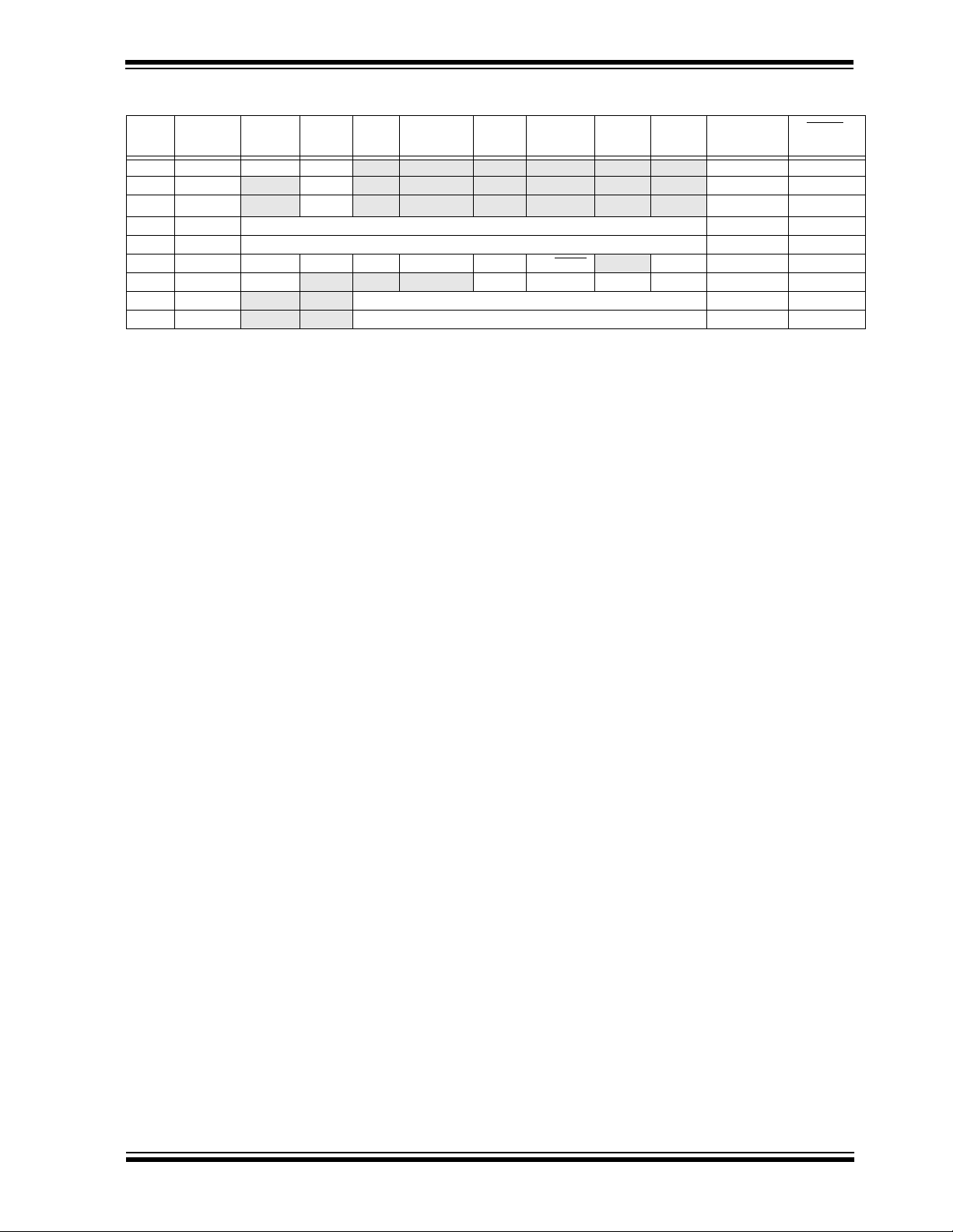
PIC16F872
TABLE 10-2: REGISTERS/BITS ASSOCIATED WITH A/D
Addr Name Bit 7 Bit 6 Bit 5 Bit 4 Bit 3 Bit 2 Bit 1 Bit 0
0Bh INTCON GIE PEIE T0IE INTE RBIE T0IF INTF RBIF 0000 000x 0000 000u
0Ch PIR1
8Ch PIE1
1Eh ADRESH A/D Result Register High Byte xxxx xxxx uuuu uuuu
9Eh ADRESL A/D Result Register Low Byte xxxx xxxx uuuu uuuu
1Fh ADCON0 ADCS1 ADCS0 CHS2 CHS1 CHS0 GO/DONE
9Fh ADCON1 ADFM
85h TRISA
05h PORTA
Legend: x = unknown, u = unchanged, - = unimplemented read as ’0’. Shaded cells are not used for A/D conversion.
Note 1: These bits are reserved; always maintain these bits clear.
(1) ADIF (1) (1) SSPIF CCP1IF TMR2IF TMR1IF r0rr 0000 r0rr 0000
(1)
— — PORTA Data Direction Register --11 1111 --11 1111
— — PORTA Data Latch when written: PORTA pins when read --0x 0000 --0u 0000
ADIE
— — — PCFG3 PCFG2 PCFG1 PCFG0 --0- 0000 --0- 0000
(1) (1) SSPIE CCP1IE TMR2IE TMR1IE r0rr 0000 r0rr 0000
—ADON0000 00-0 0000 00-0
POR,
BOR
MCLR
WDT
,
1999 Microchip Technology Inc.
Preliminary DS30221A-page 93
Page 94

PIC16F872
NOTES:
DS30221A-page 94 Preliminary
1999 Microchip Technology Inc.
Page 95

PIC16F872
11.0 SPECIAL FEATURES OF THE
CPU
These dev ices hav e a hos t of fe atures in tended to ma ximize system reliability, minimize cost through elimination of external components, provide power saving
operating modes and o ffer code protect ion . The se a r e:
• OSC Selection
• Reset
- Power-on Reset (POR)
- Powe r-up Tim er (PWRT)
- Oscillator Start-up Timer (OST)
- Brown-out Reset (BOR)
• Interrupts
• Watchdog Timer (WDT)
• SLEEP
• Code protection
• ID locations
• In-Circuit Serial Programming
• Low Voltage In-Circuit Serial Programming
• In-Circuit Debugger
These devices have a Watchdog Timer, which can be
shut off only through configuration bits. It runs off its
own RC oscillator for added reliability. There are two
timers that offer necessary delays on pow e r-up. One i s
the Oscillator Start-up Timer (OST), intended to keep
the chip in RESET until the crystal oscillator is stable.
The other is the Power-up Timer (PWRT), which provides a fixed delay of 72 ms (nominal) on power-up
only . It is designed to k eep the part in RESET while the
power supply s tab ili z e s . Wit h th es e two timers on-ch ip,
most applications need no external reset circuitry.
SLEEP mode is designed to offer a very low current
power-down mode. The user can wake-up from SLEEP
through external reset, Watchdog Timer Wake-up, or
through an interrupt. Se v er al oscil lator opt ions are also
made available to allow the part to fit the application.
The RC oscillator option saves system cost while the
LP crystal option saves power. A set of configuration
bits are used to select various options.
Additional information on special features is available
in the PICmicro™ Mid-Range Reference Manual,
(DS33023).
11.1 Configuration Bits
The configurati on bits can be prog ra mmed (read as '0')
or left unprogrammed (read as '1') to select various
device configurations. These bits are mapped in program memory location 2007h.
The user will note that address 2007h is beyond the
user program memory space. In fact, it belongs to the
special test/configuration memory space (2000h
through 3FF Fh), which can be accessed only during
programming.
1999 Microchip Technology Inc.
Preliminary DS30221A-page 95
Page 96

PIC16F872
REGISTER 11-1: CONFIGURATION WORD
CP1 CP0 DEBUG — WRT CPD LVP BODEN CP1 CP0 PWRTE WDTE F0SC1 F0SC0 Register: CONFIG
bit13 bit0
bit 13-12:
bit 5-4: CP<1:0>: Flash Program Memory Code Protection bits
11 = Code protection off
10 = 0000h to 06FFh code protected
01 = 0000h to 03FFh code protected
00 = 0000h to 07FFh code protected
bit 11: DEBUG: In-Circuit Debugger Mode
bit 10: Unimplemented: Read as ‘1’
bit 9: WRT: Flash Program Memory Write Enable
1 = Unprotected program memory may be written to by EECON control
bit 8: CPD: Data EE Memory Code Protection
1 = Code protection off
bit 7: LVP: Low Voltage In-Circuit Serial Programming Enable bit
bit 6: BODEN: Brown-out Reset Enable bit
bit 3: PWRTE
bit 2: WDTE: Watchdog Timer Enable bit
bit 1-0: FOSC1:FOSC0: Oscillator Selection bits
1 = In-Circuit Debugger disabled, RB6 and RB7 are general purpose I/O pins.
0 = In-Circuit Debugger enabled, RB6 and RB7 are dedicated to the debugger.
0 = Unprotected program memory may not be written to by EECON control
0 = Data EEPROM memory code protected
1 = RB3/PGM pin has PGM function, low voltage programming enabled
0 = RB3 is digital I/O, HV on MCLR
1 = BOR enabled
0 = BOR disabled
: Power-up Timer Enable bit
1 = PWRT disabled
0 = PWRT enabled
1 = WDT enabled
0 = WDT disabled
11 = RC oscillator
10 = HS oscillator
01 = XT oscillator
00 = LP oscillator
must be used for programming
(1)
(1)
(2)
Address 2007h
Note 1: Enabling Brown-out Reset automatically enables Power-up Timer (PWRT), regardless of the value of bit PWRTE
DS30221A-page 96 Preliminary
the Power-up Timer is enabled anytime Brown-out Reset is enabled.
2: All of the CP<1:0> pairs have to be given the same value to enable the code protection scheme listed.
1999 Microchip Technology Inc.
. Ensure
Page 97

PIC16F872
11.2 Oscillator Configurations
11.2.1 OSCILLATOR TYPES
The PIC16F872 can be operated in four different oscillator modes. The user can program two configuration
bits (FOSC1 and FOSC0) to select one of these four
modes:
• LP Low Power Crysta l
• XT Crystal/Resonator
• HS High Speed Crystal/Resonator
• RC Resistor/Capacitor
11.2.2 CRYSTAL OSCILLATOR/CERAMIC
RESONATORS
In XT, LP or HS modes, a crystal or ceramic resonator
is connected to the OSC1/CLKIN and OSC2/CLKOUT
pins to establish oscillation (Figure 11-1). The
PIC16F872 oscillator design requires the use of a parallel cut crystal. Use of a series cut crystal may give a
frequency out of the crystal manufacturers specifications. When in XT, LP or HS modes, the device can
have an external clock source to drive the OSC1/
CLKIN pin (Figure 11-2).
FIGURE 11-1: CRYSTAL/CERAMIC
RESONATOR OPERATION
(HS, XT OR LP
OSC CONFIGURATION)
(1)
C1
C2
(1)
XTAL
(2)
RS
OSC1
OSC2
RF
(3)
To
internal
logic
SLEEP
PIC16F872
TABLE 11-1: CERAMIC RESONATORS
Ranges Tested:
Mode Freq OSC1 OSC2
XT 455 kHz
2.0 MHz
4.0 MHz
HS 8.0 MHz
16.0 MHz
These values are for design guidance only. See
notes at bottom of page.
Resonators Used:
455 kHz Panasonic EFO-A455K04B ± 0.3%
2.0 MHz Murata Erie CSA2.00MG ± 0.5%
4.0 MHz Murata Erie CSA4.00MG ± 0.5%
8.0 MHz Murata Erie CSA8.00MT ± 0.5%
16.0 MHz Murata Erie CSA16.00MX ± 0.5%
All resonators used did not have built-in capacitors.
68 - 100 pF
15 - 68 pF
15 - 68 pF
10 - 68 pF
10 - 22 pF
68 - 100 pF
15 - 68 pF
15 - 68 pF
10 - 68 pF
10 - 22 pF
Note 1: See Table 11-1 and Table11-2 for rec-
ommended values of C1 and C2.
2: A series resistor (RS) may be required
for AT strip cut crystals.
3: RF varies with the crystal chosen.
FIGURE 11-2: EXTERNAL CLOCK INPUT
OPERATION (HS, XT OR LP
OSC CONFIGURATION)
Clock from
ext. system
Open
1999 Microchip Technology Inc.
OSC1
PIC16F872
OSC2
Preliminary DS30221A-page 97
Page 98

PIC16F872
TABLE 11-2: CAPACITOR SELECTION FOR
CRYSTAL OSCILLATOR
Osc
Type
Crystal
Freq
Cap. Range
C1
LP 32 kHz 33 pF 33 pF
200 kHz 15 pF 15 pF
XT 200 kHz 47-68 pF 47-68 pF
1 MHz 15 pF 15 pF
4 MHz 15 pF 15 pF
HS 4 MHz 15 pF 15 pF
8 MHz 15-33 pF 15-33 pF
20 MHz 15-33 pF 15-33 pF
These values are for design guidance only.
See notes at bottom of page.
Crystals Used
32 kHz Epson C-001R32.768K-A ± 20 PPM
200 kHz STD XTL 200.000KHz ± 20 PPM
1 MHz ECS ECS-10-13-1 ± 50 PPM
4 MHz ECS ECS-40-20-1 ± 50 PPM
8 MHz EPSON CA-301 8.000M-C ± 30 PPM
20 MHz EPSON CA-301 20.000M-C ± 30 PPM
Note 1: Highe r cap ac ita nce inc r ea se s th e st ability
of oscillator b ut also increa ses the start-up
time.
2: Since each resonator/crystal has its own
characteristics, the user should consult
the resonator/crystal manufacturer for
appropriate values of external components.
3: Rs may be required in HS mode, as well
as XT mode, to avoid overdriving crystals
with low drive level specification.
4: When migrating from other PICmicro
devices, oscillator performance should be
verified.
Cap.
Range
C2
11.2.3 RC OSCILLATOR For timing insensitive applications, the “RC” device
option offers additional cost savings. The RC oscillator
frequency is a function of the supply voltage, the resis-
EXT) and capacitor (CEXT) values, and th e ope rat-
tor (R
ing temperature. In addition to this, the oscillator
frequency will vary from unit to unit due to normal process parameter variation. Furthermore, the difference
in lead frame capacitance between package types will
also affect the oscillation frequency, especially for low
EXT values. The user also needs to take into account
C
variation du e to to leranc e of exter nal R and C com ponents used. Figure 11-3 shows how the R/C combination is connected to the PIC16F872.
FIGURE 11-3: RC OSCILLATOR MODE
VDD
REXT
OSC1
CEXT
VSS
F
Recommended values: 3 kΩ ≤ REXT ≤ 100 k
OSC/4
OSC2/CLKOUT
EXT > 20pF
C
Internal
Clock
PIC16F872
Ω
DS30221A-page 98 Preliminary
1999 Microchip Technology Inc.
Page 99

PIC16F872
11.3 Reset
Brown-out Reset (BOR). They are not affected by a
WDT Wake-up, which is viewed as the resumption of
The PIC16F872 diff eren tiates be tween v arious kinds of
reset:
• Power-on Reset (POR)
•MCLR
Reset during normal operation
•MCLR Reset during SLEEP
• WDT Reset (during normal operation)
• WDT Wake-up (during SLEEP)
• Brown-out Reset (BOR)
Some registers are not affected in any RESET condition. Their status is unknown on POR and unchanged
in any other RESET. Most other registers are reset to a
“reset state” on Power-on Reset (POR), on the MCLR
normal operation. The TO
cleared di fferently in different r eset situatio ns as indicated in Table 11-4. These bits are used in software to
determine the nature of the reset. See Table 11-6 for a
full description of reset states of all registers.
A simplified bl ock diag ram of the on-ch ip res et circui t is
shown in Figur e 11-4.
These devices have a MCLR
Reset path. The filter will detect and ignore small
pulses.
It should be noted that a WDT Reset does not drive
pin low.
MCLR
and WDT Reset, on MCLR Reset during SLEEP, and
FIGURE 11-4: SIMPLIFIED BLOCK DIAGRAM OF ON-CHIP RESET CIRCUIT
External
Reset
MCLR
SLEEP
WDT
Time-out
Reset
Power-on Reset
BODEN
VDD
WDT
Module
V
DD rise
detect
Brown-out
Reset
and PD bits are set or
noise filter in the MCLR
S
OST/PWRT
OST
10-bit Ripple counter
OSC1
(1)
On-chip
RC OSC
PWRT
10-bit Ripple counter
Enable PWRT
Enable OST
Note 1: This is a separate oscillator from the RC oscillator of the CLKIN pin.
Chip_Reset
R
Q
1999 Microchip Technology Inc.
Preliminary DS30221A-page 99
Page 100

PIC16F872
11.4 Power-On Reset (POR)
A Power-on Reset pulse is generated on-chip when
V
DD rise is detected (in the range of 1.2V - 1.7V). To
take advantage of the POR, tie the MCLR
(or through a resistor) to V
DD. This will eliminate exter-
pin directly
nal RC compone nts u sua ll y n eeded to create a Poweron Reset. A maximum rise time for VDD is specified.
See Electrical Specifications for details.
When the device starts normal operation (exits the
RESET condition), device operating parameters (voltage, frequency, temperature,...) must be m et to en su re
operation. If these conditions are not met, the device
must be held in RESET until the operating conditions
are met. Brown-out Reset may be used to meet the
start-up conditions. For additional information, refer to
Application Note , AN007, “P o wer-up Trouble Shoo ting”,
(DS00007).
11.5 Power-up Timer (PWRT)
The Power-up Timer provides a fixed 72 ms nominal
time-out on power-up only from the POR. The Powerup Timer operates on an internal RC oscillator. The
chip is kept in RESET as long as the PWRT is active.
The PWRT’ s time dela y allows V
DD to rise to an accept-
able level. A configuration bit is provided to enable/disable the PWRT.
The power-up time de la y will v ary from chip to chip due
DD, temperature and process variation. See DC
to V
parameters for details (T
PWRT, parameter #33).
11.6 Oscillator Start-up Timer (OST)
11.8 Time-out Sequence
On power-up , the Time -out Sequence is as foll ows: The
PWRT delay starts (if enabled) when a POR reset
occurs. Then OST starts counting 1024 oscillator
cycles when PWRT ends (LP, XT, HS). When the OST
ends, the device comes out of RESET.
If MCLR
expire. Bringing MCLR
is kept low long enough, the time-outs will
high will beg in execut ion im m ediately . This is useful f or testing pu rposes or to synchronize more than one PIC16CXX device operating in
parallel.
Table 11-5 shows the reset conditions for the STATUS,
PCON and PC registers, while Table 11-6 shows the
reset conditions for all the registers.
11.9 Power Control/Status Register
(PCON)
The Power Control/Status Register, PCON, has up to
two bits depending upon the device.
Bit0 is Brown-out Reset Status bit, BOR
unknown on a Power-on Reset. It must then be set by
the user and ch eck ed o n subse quent res ets to s ee if bit
cleared, indicating a BOR occurred. The BOR bit
BOR
is a "don’t care" bit and is not nece ssarily predic tabl e if
the Brown-out Reset circuitry is disabled (by clearing
bit BODEN in the Configuration Word).
Bit1 is POR
(Power-on Reset Stat us bit). It is cleared
on a Power-on Reset and unaffected otherwise. The
user must set this bit following a Power-on Reset.
. Bit BOR is
The Oscillator Start-up Timer (OST) provides 1024
oscillator cycle (from OSC1 input) delay after the
PWRT dela y i s ov er. This ensures that the crystal oscillator or resonator has started and stabilized.
The OST time-out is invoked only for XT, LP and HS
modes and only on Power-on Reset or wake-up from
SLEEP.
11.7 Brown-Out Reset (BOR)
The configuration b it, BODEN, can enable or di sable
the Brown-out Reset cir cuit. If V
(parameter D005, about 4V) for longer than TBOR
(parameter #35, a bout 100µS), the brown-ou t situation will reset the device. If V
less than T
BOR, a RESET may not occur.
Once the brown-out occu rs, the device will r emain in
Brown-out Reset until V
DD rises above VBOR. The
Power-up Timer then keeps the device in RESET for
TPWRT (parameter #33, about 72mS). If VDD should
fall below V
BOR during TPWRT, the Brown-out Reset
process will restar t when V
the Power-up Timer reset. The Power-up Timer is
always enabled when the Brown-out Reset circuit is
enabled regardless of the state of the PWRT configuration bit.
DD falls below VBOR
DD falls below VBOR for
DD rises above VBOR with
DS30221A-page 100 Preliminary
1999 Microchip Technology Inc.
 Loading...