

Page 1
MCP3204/3208
2.7V 4-Channel/8-Channel 12-Bit A/D Converters
with SPI® Serial Interface
FEATURES
• 12-bit resolution
• ± 1 LSB max DNL
• ± 1 LSB max INL (MCP3204/3208-B)
• ± 2 LSB max INL (MCP3204/3208-C)
• 4 (MCP3204) or 8 (MCP3208) input channels
• Analog inputs programmable as single-ended or
pseudo differential pairs
• On-chip sample and hold
®
serial interface (modes 0,0 and 1,1)
• SPI
• Single supply operation: 2.7V - 5.5V
• 100ksps max. sampling rate at V
• 50ksps max. sa mpling rate at V
DD
= 2.7V
DD
= 5V
• Low power CMOS technology
- 500 nA typical standby current, 2µA max.
- 400 µA max. active current at 5V
• Industrial temp range: -40°C to +85°C
• Available in PDIP, SOIC and TSSOP packages
APPLICATIONS
• Sensor Interface
• Process Control
• Data Acquisition
• Battery Operated Systems
DESCRIPTION
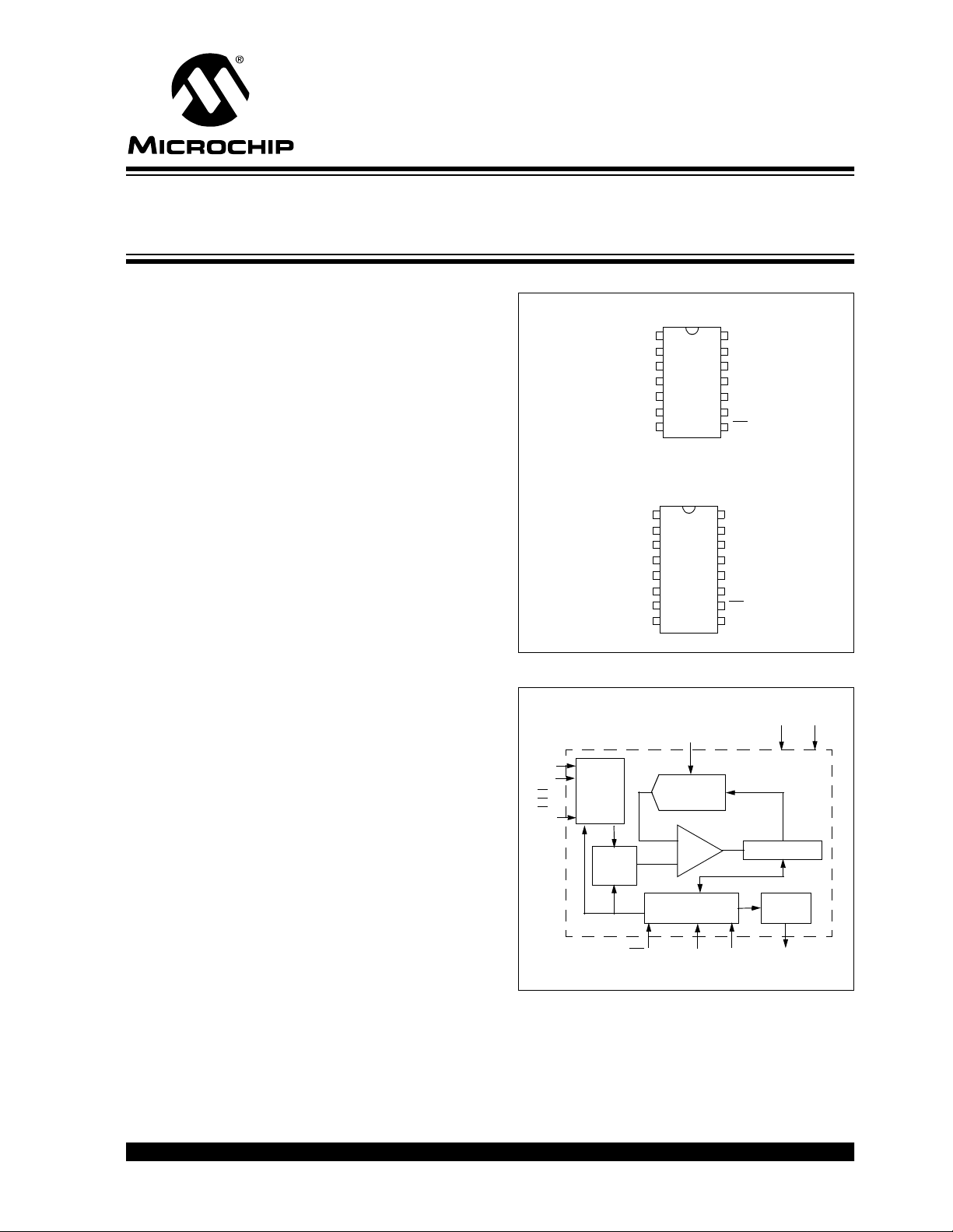
PAC K AGE TYPES
PDIP, SOIC, TSSOP
14
CH0
CH1
CH2
CH3
NC
NC
DGND
1
2
3
4
5
6
7
MCP3204
V
DD
13
V
REF
12
AGND
CLK
11
10
D
OUT
D
9
IN
8
/SHDN
CS
PDIP, SOIC
CH0
CH1
CH2
CH3
CH4
CH5
CH6
CH7
1
2
3
4
5
6
7
8
MCP3208
16
15
14
13
12
11
10
9
V
DD
V
REF
AGND
CLK
D
OUT
D
IN
CS/SHDN
DGND
FUNCTIONAL BLOCK DIAGRAM
V
V
REF
DD
V
SS
The Microchip Technology Inc. MCP3204/3208
devices are successive approximation 12-bit Analog-to-Digital (A/D) Converters with on-board sample
and hold circuitry. The MCP3204 is programmable to
provide two pseudo-differential input pairs or four single-ended inputs. The MCP3208 is programmable to
provide four pseudo-diffe rential i nput pai rs or eig ht single-ended inputs. Differential Nonlinearity (DNL) is
specified at ±1 LSB, and Integral Nonlinearity (INL) is
offered in ±1 LSB (MCP3204/3208-B) and ±2 LSB
CH0
CH1
CH7*
Input
Channel
Mux
Sample
and
Hold
DAC
Comparator
Control Logic
12-Bit SAR
Shift
Register
(MCP3204/3208-C) versions. Communication with the
devices i s done using a si mple serial interfac e compatible with the SPI protocol. The devices are capable of
conversion rates o f up to 100k sps. The MCP3204/3208
CS/SHDN
*Note: Channels 5-7 available on MCP3208 Only
D
CLK
IN
D
OUT
devices operate over a broad voltage range (2.7V -
5.5V). Low current design permits operation with typi-
cal standby and active currents of only 500nA and
320µA, respectively. The MCP3204 is offe red in 14-pin
PDIP, 150mil SOIC and TSSOP packages, and the
MCP3208 is offered in 16-pin PDIP and SOIC packages.
1999 Microchip Technology Inc. Preliminary DS21298B-page 1
Page 2
MCP3204/3208
1.0 ELECTRICAL
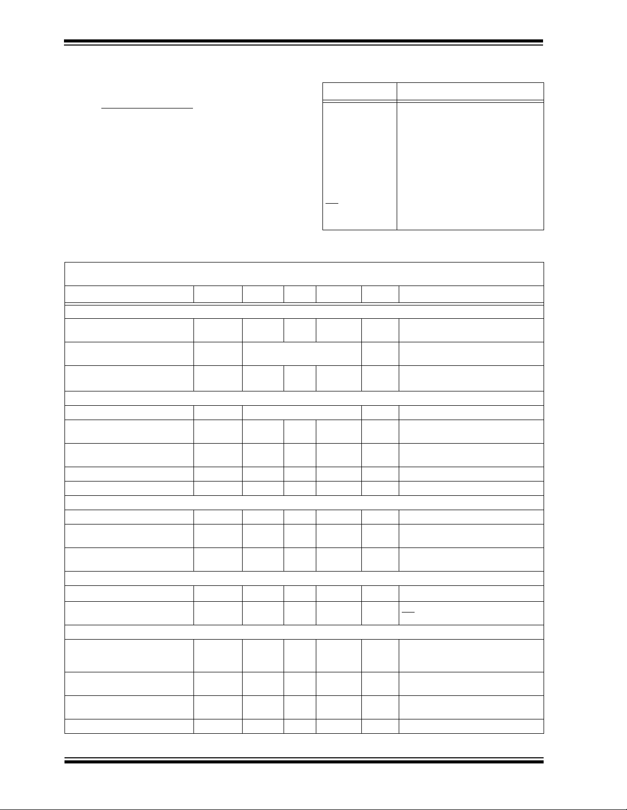
PIN FUNCTION TABLE
CHARACTERISTICS
NAME FUNCTION
1.1 Maximum Ratings*
VDD.........................................................................7.0V
All inputs and outputs w.r.t. V
Storage temperature..........................-65°C to +150°C
Ambient temp. with power applied......-65°C to +125°C
Soldering temperature of leads (10 seconds)..+300°C
ESD protection on all pins...................................> 4kV
*Notice: Stresses above those listed under “Maximum R atings” may
cause permanent damage to the device. This is a stress rating only and
functional operation of the device at those or any other conditions
above those indicated in the operational listin gs of this spe cificat ion is
not implied. Exposure to maximum rating conditions for extended periods may affect device reliability.
...... -0.6V to VDD +0.6V
SS
V
DD
DGND
AGND
CH0-CH7
CLK
D
IN
D
OUT
CS/SHDN
V
REF
+2.7V to 5.5V Power Supply
Digital Ground
Analog Ground
Analog Inputs
Serial Clock
Serial Data In
Serial Data Out
Chip Select/Shutdown Input
Reference Voltage Input
ELECTRICAL CHARACTERISTICS
All parameters apply at VDD = 5V, VSS = 0V, V
f
CLK
= 20*f
, unless otherwise noted.
SAMPLE
PARAMETER SYMBOL MIN. TYP. MAX. UNITS CONDITIONS
Convers ion Rate
Conversion Time t
Analog Input Sample Time t
Throughput Rate f
CONV
SAMPLE
SAMPLE
DC Accuracy
Resolution 12 bits
Integral Nonlinearity INL ±0.75
Differential Nonlinearity DNL ±0.5 ±1 LSB No missing codes over
Offset Error ±1.25 ±3 LSB
Gain Error ±1.25 ±5 LSB
Dynamic Performance
Total Harmonic Distortion -82 dB V
Signal to Noise and Distortion
(SINAD)
Spurious Free Dynamic
Range
Reference Input
Voltage Range 0.25 V
Current Drain 100
Analog Inputs
Input Voltage Range for
CH0-CH7 in Single-Ended
Mode
Input V oltage Rang e for IN+ In
pseudo-differential Mode
Input Voltage Range for IN - In
pseudo-differential Mode
Leakage Current 0.001 ±1 µA
REF
= 5V, T
= -40°C to +85°C, f
AMB
12 clock
cycles
1.5 clock
cycles
±1
100
50
±1
±2
ksps
ksps
LSB MCP3204/3208-B
72 dB V
86 dB VIN = 0.1V to 4.9V@1kHz
VNote2
DD
0.001
V
SS
IN- V
V
REF
150
3
REF
+IN-
µA
µA CS
V
VSS-100 VSS+100 mV
= 100ksps and
SAMPLE
V
= V
= V
REF
REF
= 5V
= 2.7V
DD
V
DD
MCP3204/3208-C
temperature
IN = 0.1V to 4.9V@1kHz
IN = 0.1V to 4.9V@1kHz
= VDD = 5V
DS21298B-page 2 Preliminary 1999 Microchip Technology Inc.
Page 3
MCP3204/3208
ELECTRICAL CHARACTERISTICS (CONTINUED)
All parameters apply at VDD = 5V, VSS = 0V, V
f
CLK
= 20*f
, unless otherwise noted.
SAMPLE
PARAMETER SYMBOL MIN. TYP. MAX. UNITS CONDITIONS
Analog Inputs (Continued)
Switch Resistance 1K Ω See Figure 4-1
Sample Capacitor 20 pF See Figure 4-1
Digital Input/Output
Data Coding Format Straight Binary
High Level Input Voltage V
Low Level Input Voltage V
High Level Output Voltage V
Low Level Output Voltage V
Input Leakage Current I
Output Leakage Current I
Pin Capacitance
(All Inputs/Outputs)
LO
CIN, C
IH
IL
OH
OL
LI
OUT
Timing Parameters
Clock Frequency f
Clock High Time t
Clock Low Tim e t
Fall To First Rising CLK
CS
Edge
Data Input Setup Time t
Data Input Hold Time t
CLK Fall To Output Data Valid t
CLK Fall To Output Enable t
CS
Rise To Output Disable t
CS
Disable Time t
Rise Time t
D
OUT
D
Fall Time t
OUT
CLK
t
SUCS
CSH
HI
LO
SU
HD
DO
EN
DIS
R
F
Power Requirements
Operating Voltage V
Operating Current I
Standby Current I
DD
320
DD
DDS
Note 1: This parameter is guaranteed by characterization and not 100% tested.
Note 2: See graphs that relate linearity performance to V
Note 3: Because the sampl e c ap wil l eventually los e c ha rge, effective clock rates below 10kHz ca n a ffec t l ine arity
performance, especially at elevated temperatures. See Section 6.2 for more information.
REF
0.7 V
= 5V, T
DD
= -40°C to +85°C, f
AMB
0.3 V
DD
V
V
= 100ksps and
SAMPLE
4.1 V IOH = -1mA, VDD = 4.5V
0.4 V IOL = 1mA, VDD = 4.5V
-10 10 µA VIN = VSS or V
-10 10 µA V
= VSS or V
OUT
DD
DD
10 pF VDD = 5.0V (Note 1)
T
= 25°C, f = 1 MHz
AMB
2.0
1.0
MHz
MHz
VDD = 5V (Note 3)
VDD = 2.7V (Note 3)
250 ns
250 ns
100 ns
50 ns
50 ns
200 ns See Test Circuits, Figure 1-2
200 ns See Test Circuits, Figure 1-2
100 ns See Test Circuits, Figure 1-2
500 ns
100 ns See Test Circuits, Figure 1-2
(Note 1)
100 ns See Test Circuits, Figure 1-2
(Note 1)
2.7 5.5 V
225
400 µA VDD = V
VDD = V
= 5V, D
REF
= 2.7V, D
REF
0.5 2 µA CS = VDD = 5.0V
levels.
REF
unloaded
OUT
unloaded
OUT
1999 Microchip Technology Inc. Preliminary DS21298B-page 3
Page 4
MCP3204/3208
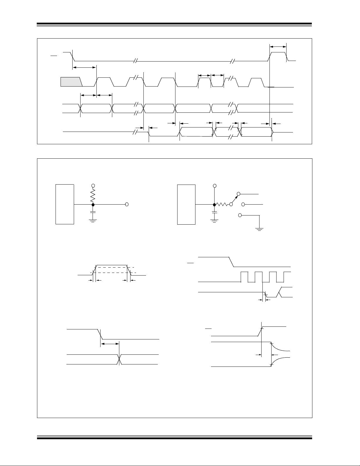
t
CSH
CS
t
SUCS
CLK
t
t
HD
SU
D
IN MSB IN
D
OUT
FIGURE 1-1: Serial Interface Timing.
Load circuit for tR, t
D
OUT
1.4V
3K
= 100pF
C
L
F, tDO
Test Point
t
t
LO
HI
t
t
EN
DO
NULL BIT
MSB OUT
t
R
Load circuit for
t
F
t
DIS
LSB
t
and t
DIS
EN
Test Point
V
DD
3K
D
OUT
100pF
V
SS
VDD/2
t
Waveform 2
DIS
tEN Waveform
t
Waveform 1
DIS
Voltage Waveforms for tR, t
D
OUT
t
R
Voltage Waveforms for t
CLK
D
OUT
F
V
OH
V
OL
t
F
DO
t
DO
CS
CLK
D
OUT
Voltage Waveforms for t
Voltage Waveforms for t
CS
D
OUT
Waveform 1*
D
OUT
EN
12
t
EN
DIS
V
IH
T
DIS
3
4
B11
90%
10%
Waveform 2†
* Waveform 1 is for an output with internal con di-
tions such that the output is high, unless disabled by the output control.
† Waveform 2 is for an output with internal condi-
tions such that the output is low, unless disabled
by the output control.
FIGURE 1-2: Test Circuits.
DS21298B-page 4 Preliminary 1999 Microchip Technology Inc.
Page 5

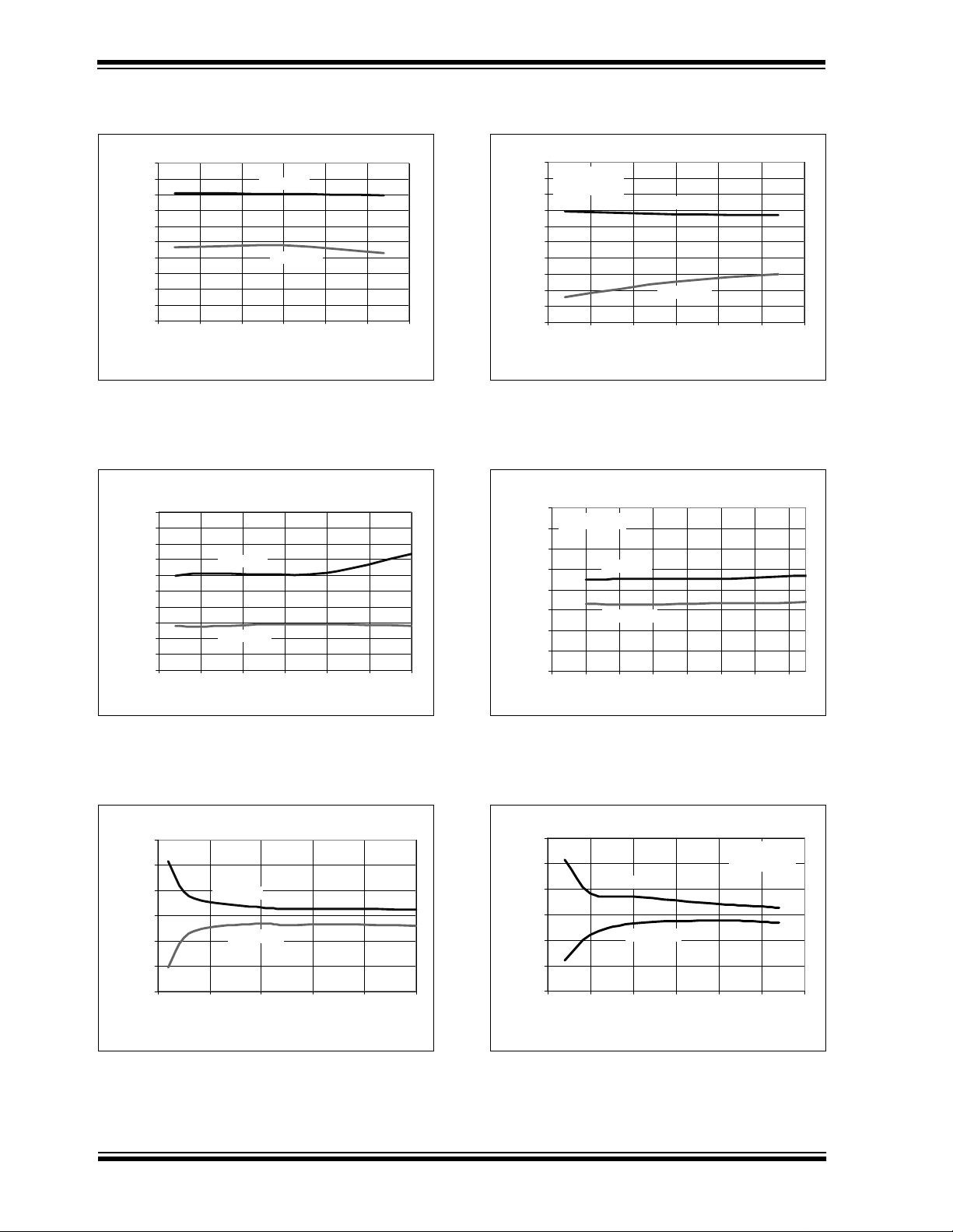
2.0 TYPICAL PERFORMANCE CHARACTERISTICS
Note: Unless otherwise indicated, V
DD
= V
= 5V, VSS = 0V, f
REF
SAMPLE
= 100ksps, f
MCP3204/3208
CLK
= 20* f
SAMPLE,TA
= 25°C
1.0
0.8
0.6
0.4
0.2
0.0
-0.2
INL (LSB)
-0.4
-0.6
-0.8
-1.0
0 25 50 75 100 125 150
Positive INL
Negative INL
Sample Rate (ksps)
FIGURE 2-1: Integral Nonlinearity (INL) vs. Sample
Rate.
3.0
2.5
2.0
1.5
1.0
0.5
0.0
-0.5
INL(LSB)
-1.0
-1.5
-2.0
-2.5
-3.0
0123456
Positive INL
Negative INL
V
(V)
REF
2.0
VDD = V
= 2.7V
1.5
1.0
0.5
0.0
-0.5
INL (LSB)
-1.0
-1.5
-2.0
REF
Positive INL
Negative INL
0 1020304050607080
Sample Rate (ksps)
FIGURE 2-4: Integral Nonl inearity (IN L) vs. Sample
Rate (V
= 2.7V).
DD
2.0
1.5
1.0
0.5
0.0
-0.5
INL(LSB)
-1.0
-1.5
-2.0
0.0 0.5 1.0 1.5 2.0 2.5 3.0
Positive INL
Negative INL
V
REF
(V)
FIGURE 2-2: Integral Nonlinearity (INL) vs. V
1.0
0.8
0.6
0.4
0.2
0.0
-0.2
INL (LSB)
-0.4
-0.6
-0.8
-1.0
0 512 1024 1536 2048 2560 3072 3584 4096
REF.
Digital Code
FIGURE 2-3: Integral Nonlinearity (INL) vs. Code
(Representative Part).
FIGURE 2-5: Integral Nonlinearity (INL) vs. V
= 2.7V).
(V
DD
1.0
VDD = V
= 2.7V
REF
= 50ksps
F
SAMPLE
0 512 1024 1536 2048 2560 3072 3584 4096
INL (LSB)
0.8
0.6
0.4
0.2
0.0
-0.2
-0.4
-0.6
-0.8
-1.0
Digital Code
FIGURE 2-6: Integral Nonlinearity (INL) vs. Code
(Representative Part, V
= 2.7V).
DD
REF
1999 Microchip Technology Inc. Preliminary DS21298B-page 5
Page 6
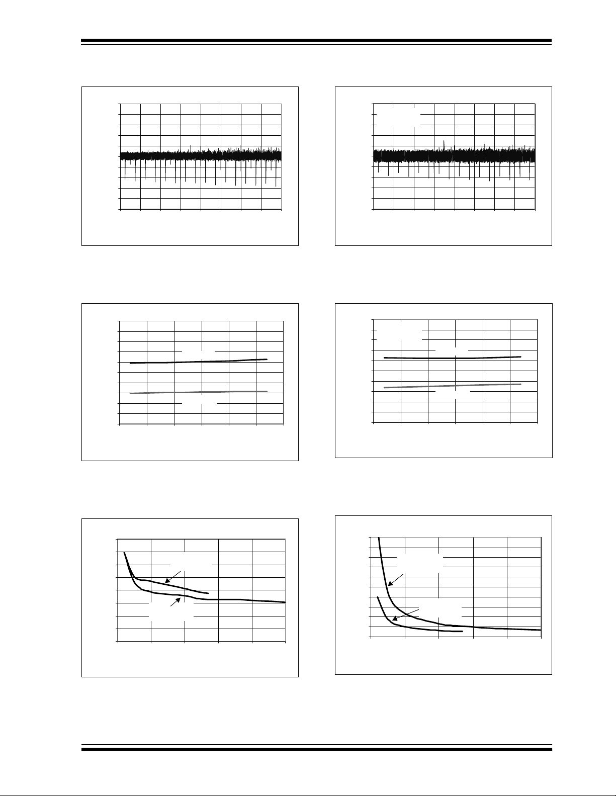
MCP3204/3208
Note: Unless otherwise indicated, V
1.0
0.8
0.6
0.4
0.2
0.0
-0.2
INL (LSB)
-0.4
-0.6
-0.8
-1.0
-50 -25 0 25 50 75 100
Positive INL
Negative INL
DD
= V
= 5V, VSS = 0V, f
REF
Temperature (°C)
FIGURE 2-7: Integral Nonlinearity (INL) vs.
Temperature.
1.0
0.8
0.6
0.4
0.2
0.0
-0.2
DNL (LSB)
-0.4
-0.6
-0.8
-1.0
0 25 50 75 100 125 150
Positive DNL
Negativ e DNL
Sample Rate (ksps)
SAMPLE
= 100ksps, f
1.0
VDD = V
0.8
F
SAMPLE
0.6
0.4
0.2
0.0
-0.2
INL (LSB)
-0.4
-0.6
-0.8
-1.0
-50 -25 0 25 50 75 100
CLK
= 2.7V
REF
= 50ksps
= 20* f
SAMPLE,TA
Positive INL
Negative INL
= 25°C
Temperature (° C )
FIGURE 2-10: Integral Nonlinearity (INL) vs.
VDD = V
= 2.7V).
DD
= 2.7V
REF
Positive DNL
Negative DNL
Sample Rate (ksps)
Temperature (V
2.0
1.5
1.0
0.5
0.0
-0.5
DNL (LSB)
-1.0
-1.5
-2.0
0 10203040506070
FIGURE 2-8: Differential Nonlinearity (DNL) vs.
Sample Rate.
3.0
2.0
1.0
0.0
DNL (LSB)
-1.0
-2.0
-3.0
012345
Positive DNL
Negative DNL
V
(V)
REF
FIGURE 2-9: Differential Nonlinearity (DNL) vs.
V
REF.
FIGURE 2-11: Differential Nonlinearity (DNL) vs.
.
= 2.7V).
DD
Positive DNL
Negative DNL
V
REF
(V)
VDD = V
F
SAMPLE
= 2.7V
REF
= 50ksps
REF
Sample Rate (V
3.0
2.0
1.0
0.0
DNL (LSB)
-1.0
-2.0
-3.0
0.00.51.01.52.02.53.0
FIGURE 2-12: Differe nti al N onl ine arity (DNL) vs . V
(VDD = 2.7V)
DS21298B-page 6 Preliminary 1999 Microchip Technology Inc.
Page 7
MCP3204/3208
)
)
Note: Unless otherwise indicated, V
1.0
0.8
0.6
0.4
0.2
0.0
-0.2
DNL (LSB)
-0.4
-0.6
-0.8
-1.0
0 512 1024 1536 2048 2560 3072 3584 4096
DD
= V
= 5V, VSS = 0V, f
REF
Digital Code
FIGURE 2-13: Differential Nonlinearity (DNL) vs.
Code (Representative Par t).
1.0
0.8
0.6
0.4
0.2
0.0
-0.2
DNL (LSB)
-0.4
-0.6
-0.8
-1.0
-50 -25 0 25 50 75 100
Positive DNL
Negative DNL
Temper at ure (°C)
SAMPLE
= 100ksps, f
1.0
VDD = V
0.8
F
SAMPLE
0.6
0.4
0.2
0.0
-0.2
DNL (LSB)
-0.4
-0.6
-0.8
-1.0
0 512 1024 1536 2048 2560 3072 3584 4096
CLK
= 2.7V
REF
= 50ksps
= 20* f
SAMPLE,TA
= 25°C
Digital C ode
FIGURE 2-16: Differential Nonlinearity (DNL) vs.
Code (Representative Part, V
1.0
VDD = V
= 2.7V
0.8
0.6
0.4
0.2
0.0
-0.2
DNL (LSB)
-0.4
-0.6
-0.8
-1.0
REF
= 50ksps
F
SAMPLE
-50 -25 0 25 50 75 100
Temperat ur e (°C)
DD
Positive DNL
Negative DNL
= 2.7V).
FIGURE 2-14: Differential Nonlinearity (DNL) vs.
Temperature.
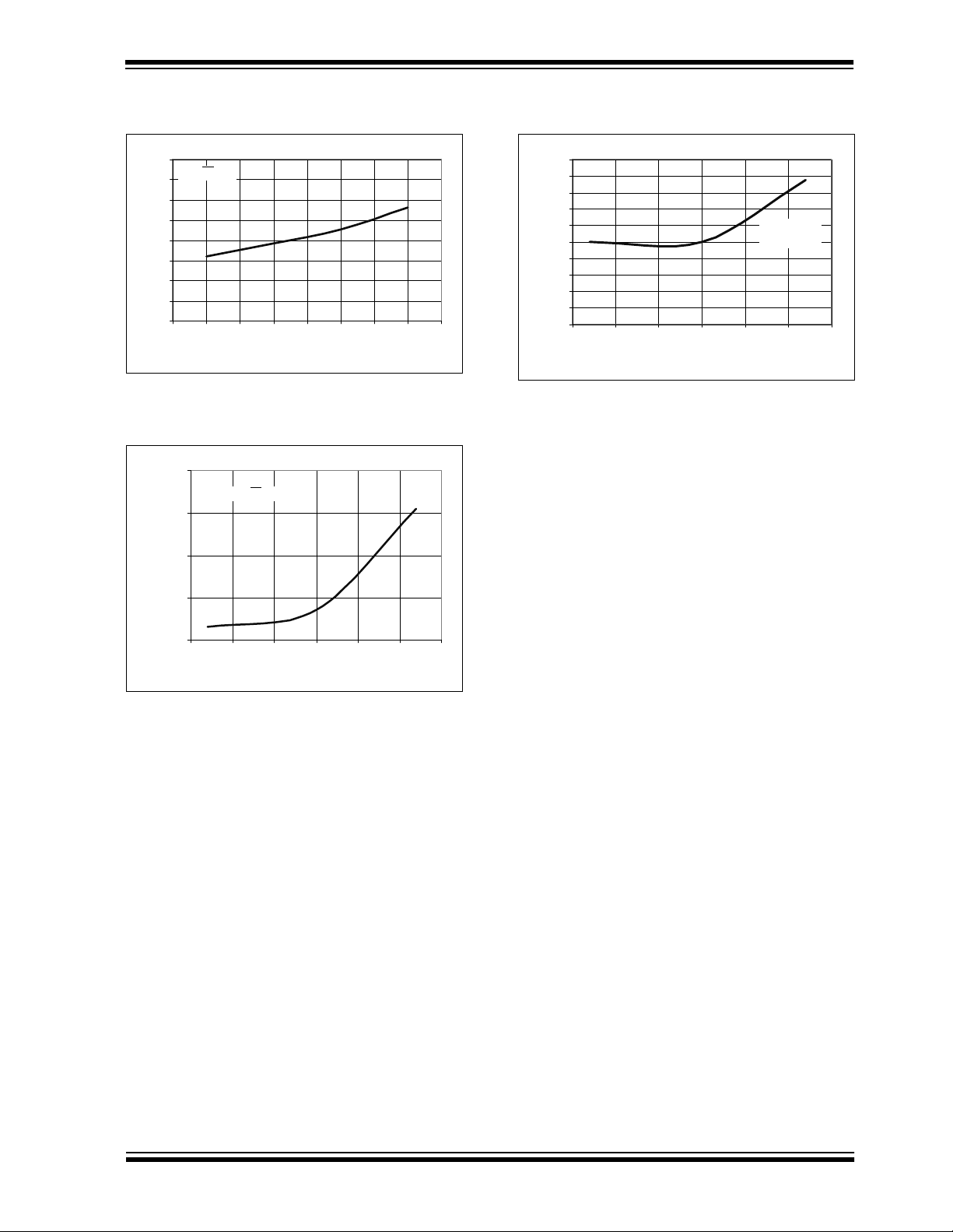
4
3
2
1
0
-1
Gain Error (LSB
-2
-3
-4
012345
FIGURE 2-15: Gain Error vs. V
VDD = 5V
F
SAMPLE
VDD = 2.7V
F
SAMPLE
= 100ksps
= 50ksps
V
REF
(V)
REF.
FIGURE 2-17: Differential Nonlinearity (DNL) vs.
Temperature (V
20
18
16
14
12
10
8
6
Offset Error (LSB
4
2
0
012345
FIGURE 2-18: Offset Error vs. V
= 2.7V).
DD
VDD = 5V
F
SAMPLE
= 100ksps
VDD = 2.7V
F
SAMPLE
= 50ksps
V
REF
(V)
REF.
1999 Microchip Technology Inc. Preliminary DS21298B-page 7
Page 8

MCP3204/3208
)
)
)
Input S ignal Level ( dB )
)
Note: Unless otherwise indicated, V
0.2
0.0
-0.2
-0.4
-0.6
-0.8
-1.0
-1.2
Gain Error (LSB
-1.4
-1.6
-1.8
VDD = V
= 2.7V
REF
= 50ks ps
F
SAMPLE
VDD = V
= 5V
REF
= 100ksps
F
SAMPLE
-50 -25 0 25 50 75 100
DD
= V
Temper at ur e ( °C)
FIGURE 2-19: Gain Error vs. Temperature.
100
90
80
70
60
50
SNR (dB)
40
30
20
VDD = V
F
SAMPLE
= 2.7V
REF
= 50ksps
10
0
1 10 100
Input Fr equency (kHz)
VDD = V
F
SAMPLE
= 5V, VSS = 0V, f
REF
= 5V
REF
= 100k sps
SAMPLE
= 100ksps, f
2.0
1.8
1.6
1.4
1.2
1.0
0.8
0.6
Offset Error (LSB
0.4
0.2
0.0
-50 -25 0 25 50 75 100
CLK
VDD = V
F
VDD = V
F
= 20* f
REF
= 100ksps
SAMPLE
REF
= 50ksps
SAMPLE
SAMPLE,TA
= 5V
= 2.7V
= 25°C
Temperature (°C)
FIGURE 2-22: Offset Error vs. Temperature.
100.0
90.0
80.0
70.0
60.0
50.0
40.0
SINAD (dB
30.0
VDD = V
F
SAMPLE
= 2.7V
REF
= 50ksps
20.0
10.0
0.0
1 10 100
Input F r equency (kHz)
VDD = V
F
SAMPLE
= 5V
REF
= 100ksps
FIGURE 2-20: Signal to Noise (SNR) vs. Input
Frequency.
0
-10
-20
-30
-40
-50
-60
THD (dB)
-70
-80
-90
-100
110100
VDD = V
F
SAMPLE
= 2.7V
REF
= 50ksps
VDD = V
F
SAMPLE
= 5V
REF
= 100ksps
FIGURE 2-23: Signal to Noise and Distortion
(SINAD) vs. Input Frequency.
80
70
60
50
40
30
SINAD (dB
20
10
0
-40 -35 -30 -25 -20 -15 -10 -5 0
VDD = V
F
SAMPLE
= 5V
REF
= 100ksps
VDD = V
F
SAMPLE
= 2.7V
REF
= 50ksps
Input Frequency (kHz )
FIGURE 2-21: Total Harmonic Distortion (THD) vs.
Input Frequency.
DS21298B-page 8 Preliminary 1999 Microchip Technology Inc.
FIGURE 2-24: Signal to Noise and Distortion
(SINAD) vs. Input Signal Level.
Page 9

MCP3204/3208
)
Note: Unless otherwise indicated, V
12.00
11.75
11.50
11.25
11.00
10.75
10.50
10.25
10.00
ENOB (rms)
9.75
9.50
9.25
9.00
0.0 0.5 1.0 1.5 2.0 2.5 3.0 3.5 4.0 4.5 5.0
VDD = V
F
SAMPLE
= 2.7V
REF
= 50ksps
V
REF
(V)
DD
= V
VDD = V
F
SAMPLE
= 5V, VSS = 0V, f
REF
= 5V
REF
=100ksps
FIGURE 2-25: Effective Number of Bits (ENOB) vs.
V
REF.
100
90
80
70
60
VDD = V
SFDR (dB)
50
40
30
F
SAMPLE
= 2.7V
REF
= 50ksps
20
10
0
1 10 100
Input Frequency (kHz)
VDD = V
F
SAMPLE
= 5V
REF
= 100ksps
SAMPLE
= 100ksps, f
CLK
= 20* f
SAMPLE,TA
= 25°C
12.0
11.5
11.0
10.5
10.0
9.5
ENOB (rms)
9.0
8.5
VDD = V
F
SAMPLE
= 2.7V
REF
= 50ksps
VDD = V
F
SAMPLE
= 5V
REF
= 100ksps
8.0
110100
Input F r equency (kH z)
FIGURE 2-28: Effective Number of Bits (ENOB) vs.
Input Frequency.
0
-10
-20
-30
-40
-50
-60
-70
Power Supply Rejection (dB
-80
1 10 100 1000 10000
Ripple Frequ ency (kH z)
FIGURE 2-26: Spurious Free Dynamic Range
(SFDR) vs. Input Frequency.
0
-10
-20
-30
-40
-50
-60
-70
-80
-90
Amplitude (dB)
-100
-110
-120
-130
0 10000 20000 30000 40000 50000
VDD = V
REF
F
= 100ksps
SAMPLE
F
= 9.985kHz
INPUT
4096 points
= 5V
Frequency (Hz)
FIGURE 2-27: Frequency Spectrum of 10kHz input
(Representative Part).
FIGURE 2-29: Power Supply Rejection (PSR) vs.
Ripple Frequency.
0
-10
-20
-30
-40
-50
-60
-70
-80
-90
Amplitude (dB)
-100
-110
-120
-130
0 5000 10000 15000 20000 25000
VDD = V
REF
= 50ksps
F
SAMPLE
= 998.76Hz
F
INPUT
4096 points
= 2.7V
Fr equ ency ( Hz)
FIGURE 2-30: Frequency Spectrum of 1kHz input
(Representative Part, V
= 2.7V).
DD
1999 Microchip Technology Inc. Preliminary DS21298B-page 9
Page 10

MCP3204/3208
Note: Unless otherwise indicated, V
500
V
= V
REF
450
400
350
300
250
(µA)
DD
I
200
150
100
50
0
2.0 2.5 3.0 3.5 4.0 4.5 5.0 5.5 6.0
FIGURE 2-31: I
400
350
300
250
200
(µA)
DD
I
150
100
50
0
10 100 1000 10000
DD
All points at F
at V
= VDD = 2.5V, F
REF
DD
VDD = V
= 2MHz except
CLK
= 1MHz
CLK
VDD (V)
vs. V
DD.
= 5V
REF
VDD = V
= 2.7V
REF
Clock F r equency (kHz)
DD
= V
= 5V, VSS = 0V, f
REF
= 100ksps, f
SAMPLE
100
90
80
70
60
(µA)
50
REF
40
I
30
20
10
0
2.02.53.03.54.04.55.05.56.0
FIGURE 2-34: I
100
90
80
70
60
(µA)
50
REF
40
I
30
20
10
0
10 100 1000 10000
CLK
V
REF = VDD
All points at F
= VDD = 2.5V, F
at V
REF
REF
= 20* f
= 2MHz except
CLK
CLK
SAMPLE,TA
= 1MHz
= 25°C
VDD (V)
vs. V
DD.
VDD = V
= 5V
REF
VDD = V
= 2.7V
REF
Clock F r equency (kHz)
FIGURE 2-32: I
400
350
300
250
200
(µA)
DD
I
150
100
50
0
-50 -25 0 25 50 75 100
FIGURE 2-33: I
vs. Clock Frequency.
DD
VDD = V
= 5V
REF
= 2MHz
F
CLK
VDD = V
= 2.7V
REF
= 1MHz
F
CLK
Tem p erature ( °C)
vs. Temperature.
DD
FIGURE 2-35: I
100
90
80
70
60
(µA)
50
REF
I
40
30
20
10
0
-50 -25 0 25 50 75 100
vs. Clock Frequency.
REF
VDD = V
= 2MHz
F
CLK
VDD = V
= 2.7V
REF
= 1MHz
F
CLK
= 5V
REF
Temperat ur e ( ° C )
FIGURE 2-36: I
vs. Temperature.
REF
DS21298B-page 10 Preliminary 1999 Microchip Technology Inc.
Page 11
MCP3204/3208
Note: Unless otherwise indicated, V
80
V
= CS = V
REF
70
60
50
40
IDDS (pA)
30
20
10
0
2.0 2.5 3.0 3.5 4.0 4.5 5.0 5.5 6.0
DD
DD
VDD (V)
FIGURE 2-37: I
100.00
10.00
(nA)
1.00
DDS
I
VDD = V
DDS
REF
vs. V
= CS = 5V
DD.
= V
= 5V, VSS = 0V, f
REF
SAMPLE
= 100ksps, f
2.0
1.8
1.6
1.4
1.2
1.0
0.8
0.6
0.4
0.2
Analog Input Leakage (nA)
0.0
-50 -25 0 25 50 75 100
CLK
= 20* f
SAMPLE,TA
= 25°C
VDD = V
F
CLK
REF
= 2MHz
= 5V
Temperat ure ( ° C)
FIGURE 2-39: Analog Input Leakage Current vs.
Temperature.
0.10
0.01
-50 -25 0 25 50 75 100
FIGURE 2-38: I
Temperat ur e (°C)
vs. Temperature.
DDS
1999 Microchip Technology Inc. Preliminary DS21298B-page 11
Page 12

MCP3204/3208
3.0 PIN DESCRIPTIONS
3.1 CH0 - CH7
Analog inputs for channels 0 - 7 respectively for the
multiplexed inputs. Each pair of channels can be programmed to be used as two independent channels in
single ended-mode or as a single pseudo-differential
input where one chan nel is IN+ an d one chann el is IN-.
See Section 4.1 and Section 5.0 for information on programming the channel configuration.
3.2 CS/SHDN(Chip Select/Shutdown)
The CS/SHDN pin is used to initiate communication
with the device when pulled low and will end a conversion and put the device in low power standby when
pulled high. The CS
between conversions.
3.3 CLK (Serial Clock)
The SPI clock pin is used to initiate a conversion and to
clock out each bit of the conversion as it takes place.
See Section 6.2 for constraints on clock speed.
3.4 DIN (Serial Data Input)
The SPI port serial data input pin is used to load channel configuration data into the device.
3.5 DOUT (Serial Data output)
The SPI serial data output pin is used to shift out the
results of the A/D conversion. Data will always change
on the falling edge of each clock as the conversion
takes place.
3.6 AGND
Analog ground connection to internal analog circuitry.
3.7 DGND
/SHDN pin must be pulled high
4.1 Analog Inputs
The MCP3204/3208 devices offer the choice of using
the analog input channels configured as single-ended
inputs or pseudo-differential pairs. The MCP3204 can
be configured to provide two pseudo-differential input
pairs or four single-ende d inpu ts. the MCP32 08 can b e
configured to provide four pseudo-differential input
pairs or eight single-ended inputs. Configuration is
done as part of the serial command before each conversion begins. When used in the pseudo-differential
mode, each chan nel pa ir (i .e ., C H0 an d C H1, C H2 an d
CH3 etc.) are prog rammed as t he IN+ and IN- inputs as
part of the command string transmitted to the device.
The IN+ input can range from IN- to (V
IN- input is limited to ±100m V from the V
input can be used to cancel small signal common-mode noise which is present on both the IN+ and
IN- inputs.
When operating in the pseudo-differential mode, if the
voltage level of IN+ is equal to or less than IN-, the
resultant code wi ll be 000h. If t he voltag e at IN+ is e qual
to or greater than {[V
+ (IN-)] - 1 LSB}, then the out-
REF
put code will be FFFh . If the v olta ge level at IN- is more
than 1 LSB below VSS, then the v olt age level at the IN+
input will have to go below V
to see the 000h output
SS
code. Conv ersely, if IN- is more than 1 LSB ab ov e V
then the FFFh code wil l not be seen unless the IN+
input level goes above V
REF
level .
For the A/D Con verter to meet spe cification, the charge
holding capacito r , (C
) must be giv en enou gh time
SAMPLE
to acquire a 12-bit accu rate voltage leve l durin g the 1 .5
clock cycl e s am pl ing pe riod. The analog input model i s
shown in Figure 4-1.
In this diagram it is shown that the source impedance
) adds to the internal sampling switch (RSS) imped-
(R
S
ance, directly affecting the time that is required to
charge the capacitor, C
. Consequently, larger
SAMPLE
source impedances increase the offset, gain, and integral linearity errors of the conversion. See Figure 4-2.
+ IN-). The
REF
rail. The IN-
SS
SS
,
Digital ground connection to internal digital circuitry.
4.0 DEVICE OPERATION
The MCP3204/3208 A/D Con v erters emplo y a conv e ntional SAR architecture. With this architecture, a sample is acquired on an in ternal sa mple/h old c apaci tor for
1.5 clock cycles s tarting on the fou rth rising edge o f the
serial clock after the start bit has been recei ved. F ollowing this sample time, the device uses the collected
charge on the internal sample and hold capacitor to
produce a serial 12-bit digital output code. Conversion
rates of 10 0ksps are possible on t he MCP3204 /3208.
See Section 6.2 for information on minimum clock
rates. Communication with the device is done using a
4-wire SPI-compatible interface.
4.2 Reference Input
For each de vice in the family, the referen ce input (V
determines the analog input voltage range. As the reference input is reduced, the LSB size is reduced
accordingly. The theoretical digital output code produced by the A/D Converter is a function of the analog
input signal and the reference input as shown below.
Digital Output Code = 4096 * V
IN
V
REF
where:
VIN = analog input voltage
V
= reference volta ge
REF
When using an external voltage reference device, the
system designer should always refer to the manufac-
REF
turer’s recommendations for c ircuit la you t. Any instabi lity in the operation of the reference device will have a
direct effect on the operation of the A/D Converter.
DS21298B-page 12 Preliminary 1999 Microchip Technology Inc.
)
Page 13

VA
)
Legend
I
LEAKAGE
C
SAMPLE
CHx
R
S
C
7pF
VA
= Signal Source
R
= Source Impedance
S
CHx
= Input Channel Pad
C
= Input Capacitance
PIN
V
= Threshold Voltage
T
= Leakage Current at the pin
due to various junctions
SS
= Sampling Switch
R
= Sampling Switch Resistor
SS
= Sample/Hold Capacitance
PIN
MCP3204/3208
V
DD
= 0.6V
V
T
V
= 0.6V
T
I
LEAKAGE
± 1 nA
Sampling
Switch
R
SS
SS
= 1kΩ
C
SAMPLE
= DAC capacitance
= 20 pF
V
SS
FIGURE 4-1: Analog Input Model
2.5
2.0
1.5
1.0
0.5
Clock Frequency (MHz
0.0
100 1000 10000
VDD = 5V
VDD = 2.7V
Input R e si st a nce (O h m s)
FIGURE 4-2: Maximum Clock Frequency vs. Input
resistance (R
) to maintain less than a 0.1LSB
S
deviation in INL from nominal conditions.
1999 Microchip Technology Inc. Preliminary DS21298B-page 13
Page 14

MCP3204/3208
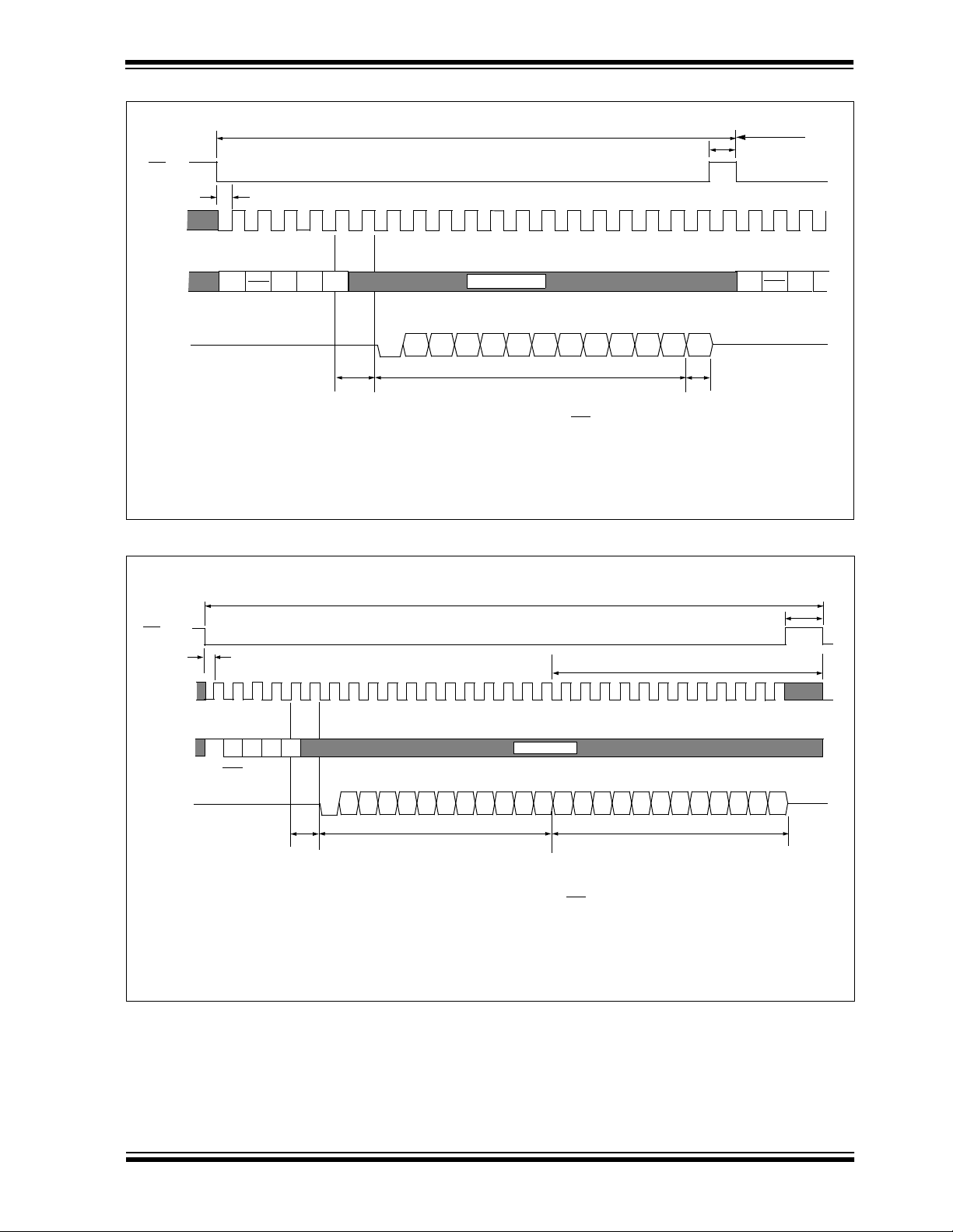
5.0 SERIAL COMMUNICATIONS
Communication with the MCP3204/3208 devices is
done using a standard SPI-compatible serial interface.
Initiating communication with either device is done by
bringin g the CS
was powered up with the CS
high and back low to initiate communication. The first
clock received with CS low a nd DIN high will constitute
a start bit. The SGL/DIFF
determ ine if the conversion will be done using single
ended or differential input mode. The next three bits
(D0, D1 and D2) are used to select the input channel
configuration. Tab le 5-1 and Tab le5-2 show the configuration bits for the MCP3204 and MCP3208, respectively. The device will begin to sample the analog input
on the fourth ri sing e dge of th e cl ock afte r the sta r t bit
has been rec eived. Th e samp le per iod wi ll end on the
falling edge of the fifth clock following the start bit.
After the D0 bit is input, one more clock is required to
complete the sample and hold period (D
care for this cloc k). On the falli ng edge of the ne xt cloc k,
the device will output a low null bit. The next 12 clocks
will output the result of th e con ve rsion with MSB fir st as
shown in Figure 5-1. Data is always output from the
device on t he falling edge of the cl ock . If all 12 data bits
have been transmitted and the device continues to
receive clocks wh ile t he CS
output the conversion result LSB first as shown in
Figure 5-2. If more clocks are provided to the device
while CS
transmitted), the device will clock o ut zeros indefinitely.
If necessary, it is po s si ble t o bring CS
leading zeros on th e D
often done when dealing with microcontroller-based
SPI ports that must send 8 bits at a time. Refer to
Section 6.1 for more details on using the
MCP3204/3208 devices with hardware SPI ports.
line low. See Figure 5-1. If the device
pin low , it m ust be br ought
bit follows the st art bit and will
is a don’t
IN
is held low, the device will
is still low (after the LSB first data has been
low and clock in
line before the start bit. This is
IN
CONTROL BIT
SINGLE/
DIFF
SELECTIONS
D2 D1 D0
INPUT
CONFIGURATION
CHANNEL
SELECTION
1 0 0 0 single ended CH0
1 0 0 1 single ended CH1
1 0 1 0 single ended CH2
1 0 1 1 single ended CH3
1 1 0 0 single ended CH4
1 1 0 1 single ended CH5
1 1 1 0 single ended CH6
1 1 1 1 single ended CH7
0 0 0 0 differential CH0 = IN+
CH1 = IN-
0 0 0 1 differential CH0 = IN-
CH1 = IN+
0 0 1 0 differential CH2 = IN+
CH3 = IN-
0 0 1 1 differential CH2 = IN-
CH3 = IN+
0 1 0 0 differential CH4 = IN+
CH5 = IN-
0 1 0 1 differential CH4 = IN-
CH5 = IN+
0 1 1 0 differential CH6 = IN+
CH7 = IN-
0 1 1 1 differential CH6 = IN-
CH7 = IN+
TABLE 5-2: Configuration Bits for the MCP3208.
CONTROL BIT
SINGLE/
DIFF
SELECTIONS
D2* D1 D0
INPUT
CONFIGURATION
CHANNEL
SELECTION
1 X 0 0 single ended CH0
1 X 0 1 single ended CH1
1 X 1 0 single ended CH2
1 X 1 1 single ended CH3
0 X 0 0 differential CH0 = IN+
CH1 = IN-
0 X 0 1 differential CH0 = IN-
CH1 = IN+
0 X 1 0 differential CH2 = IN+
CH3 = IN-
0 X 1 1 differential CH2 = IN-
CH3 = IN+
*D2 is don’t care for MCP3204
TABLE 5-1: Configuration Bits for the MCP3204.
DS21298B-page 14 Preliminary 1999 Microchip Technology Inc.
Page 15
MCP3204/3208
t
CYC
t
CSH
CS
t
SUCS
CLK
SGL/
D
IN
D
OUT
Start
DIFF
HI-Z
D1D2 D0
t
SAMPLE
Don’t Care
Null
B11 B10 B9 B8 B7 B6 B5 B4 B3 B2 B1 B0 *
Bit
t
CONV
t
DATA
Start
HI-Z
**
* After completing the data tran sfer , if f urther clocks are a pplied w ith CS low, the A/D Conv erter will output LSB
first data, then followed with zeros indefinitely. See Figure 5-2 below.
: during this time, the bias current and the comparator power down while the reference input becomes
** t
DATA
a high impedance node, leaving the CLK running to clock out the LSB-first data or zeros.
FIGURE 5-1: Communication with the MCP3204 or MCP3208.
t
CYC
SGL/
DIFF
D2
t
CYC
t
CS
t
SUCS
Power Down
CSH
CLK
D
IN
D
OUT
Start
SGL/
DIFF
HI-Z
D0D1D2
t
SAMPLE
Don’t Care
Null
B11 B10B9B8 B7 B6 B5 B4 B3 B2 B1 B0 B1 B2 B3 B4 B5 B6 B7 B8 B9 B10 B11
Bit
(MSB)
t
t
CONV
DATA
**
* After completing the data trans fer, i f further clocks ar e applied with C S low , the A/D Conve rter will output zeros
indefinitely.
: During this time , the bi as c irc uit a nd the comparator power d o w n whi le the reference input becomes a
** t
DATA
high impedance node, leaving the CLK running to clock out LSB first data or zeroes.
FIGURE 5-2: Communication with MCP3204 or MCP3208 in LSB First Format.
HI-Z
*
1999 Microchip Technology Inc. Preliminary DS21298B-page 15
Page 16
MCP3204/3208
6.0 APPLICATIONS INFORMATION
6.1 Using the MCP3204/3208 with Microcontroller (MCU) SPI Ports
With most microcontroller SPI ports, it is required to
send groups of eight bits. It is also required that the
microcontroller SPI port be configured to clock out data
on the falling edge of cloc k and latch data in on the rising
edge. Because communication with the MCP32 04/3208
devices ma y not need m ultiple s of eigh t clocks, it will be
necessary to provide more clocks than are required.
This is usually done by sending ‘leading zeros’ before
the start bit. As an example, Figure6-1 and Figure 6-2
shows how the MCP3204/3208 can be interfaced to a
MCU with a hardware SPI port. Figure 6-1 depicts the
operation shown in SPI Mode 0,0 which requires that the
SCLK from the MCU idles in the ‘low’ state, while
Figure 6-2 shows the similar case of SPI Mode 1,1
where the clock idles in the ‘high’ state .
CS
MCU latches data from A/D Converter
on rising edges of SCLK
SCLK
D
IN
1 2 3 4 5 6 7 8 910111213141516
Data is clocked out of
A/D Converter on falling edges
SGL/
Start
DIFF
D2
DO
D1
As shown in Figure 6-1, the first byte transmitted to the
A/D Converter contains five leading zeros before the
start bit. Arranging the leading zeros this way produces
the output 12 bits to fall in positions easily manipulated
by the MCU. The MSB is clocked out of the A/D Converter on the falling edge of clock number 12. After the
second eight clocks have been sent to the device, the
MCUs receive buffer will contain three unknown bits
(the output is at high impedance for the first two clocks),
the null bit and the highest order four bits of the conversion. After the third byte has been sent to the device, the
receive register will contain the lowest order eight bits of
the conversion results. Easier manipulation of the converted data can be obtained by using this method.
Figure 6-2 shows the same thing in SPI Mode 1,1
which requires that the clock idles in the high state. As
with mode 0,0, the A/D Converter outputs data on the
falling edge of the c lock a nd the MCU la tches data from
the A/D Converter in on the rising edge of the clock.
17 18 19 20 21 22 23 24
Don’t Care
D
OUT
MCU Transmitted Data
(Aligned with falling
edge of clock)
MCU Received Data
(Aligned with rising
edge of clock)
X = Don’t Care Bits
HI-Z
Start
Bit
00000
????????
Data stored into MCU receive register
after transmission of first 8 bits
SGL/
D2
1
DIFF
???
Data stored into MCU receive r egister
NULL
B11 B10 B9 B8
BIT
DO XXXXX XXX
D1
X
XX XXX
B11 B10 B9 B80
(Null)
after transmission of second 8 bits
B7 B6 B5 B4 B3 B2 B1 B0
B7 B6 B5 B4 B3 B2 B1 B0
Data stored into MCU receive re gister
FIGURE 6-1: SPI Communication using 8-bit segments (Mode 0,0: SCLK idles low).
CS
MCU latches data from A/D Converter
on rising edges of SCLK
SCLK
D
IN
D
OUT
MCU Transmitted Data
(Aligned with falling
edge of clock)
MCU Received Data
(Aligned with rising
edge of clock)
1 2 3 4 5 6 7 8 9101112131415 16
Data is clocked out of
A/D Converter on falling edges
SGL/
D2
D1
Start
DIFF
HI-Z
Start
Bit
00000
????????
SGL/
D2
1
DIFF
DO
DO
D1
???
NULL
B11 B10 B9
BIT
X
XX XXX
B11 B10 B9 B80
(Null)
17 18 19 20 21 22 23 24
Don’t Care
B7
B8
XXXXX XXX
B7 B6 B5 B4 B3 B2 B1 B0
after transmission of last 8 bits
B6 B5 B4 B3 B2 B1 B0
X = Don’t Care Bits
Data stored into MCU receive r egister
after transmission of first 8 bits
Data stored into MCU receive r egister
after transmission of second 8 bits
Data stored into MCU receive reg ister
after transmission of last 8 bits
FIGURE 6-2: SPI Communication using 8-bit segments (Mode 1,1: SCLK idles high).
DS21298B-page 16 Preliminary 1999 Microchip Technology Inc.
Page 17
MCP3204/3208
6.2 Maintaining Minimum Clock Speed
When the MCP3204/3208 initiates the sample period,
charge is stored on the sample capacitor. When the
sample period is complete, the device converts one bit
for each clock that is received. It is impor tant for the
user to note that a slow clock rate will allow charge to
bleed off the s ample cap acitor w hile th e conversion is
taking place. At 85°C (worst case condition), the part
will maintain prope r charge on the sa mple capac itor for
at least 1.2ms afte r the sa mp le period has ended. This
means that the time between the end of the sample
period and the time that all 12 data bits have been
clocked o ut mu st not exceed 1.2ms (effectiv e cl oc k frequency of 10kHz). Failure to meet this criterion may
induce linearity errors into the conversion outside the
rated specif icat ions. It sh ould b e note d that du ri ng the
entire conversion cycle, the A/D Converter does not
require a constant cloc k speed or du ty cycle, as long as
all timing specification s are met .
6.3 Buffering/Filtering the Analog Inputs
If the signal source for the A/D Converter is not a low
impedance source , it will ha v e to be b uffered or inaccurate conversion results may occur. See Figure 4-2. It is
also recommended that a fil ter be used to eliminate an y
signals that may be aliased back in to the conversion
results. This is illustrated in Figure 6-3 where an op
amp is used to drive the analog input of the
MCP3204/3208. This amplifier provides a low impedance source for the converter input and a low pass filter, which eliminates unwanted high frequency noise.
Low pass (anti-aliasing) filters can be designed using
Microchip’s f ree interactive FilterLab™ software. Fil-
terLab will calculate capacitor and resistors values, as
well as determine the number of poles that are required
for the application. F or more information o n filtering sig-
V
REF
IN+
MCP3204
IN-
“Anti-Aliasing
V
DD
10µF
1µF
nals, see the application note AN699
Analog Filters for Data Acquisition Systems.”
4.096V
Reference
0.1µF
C
1
R
1
V
IN
R
MCP601
2
C
2
R
3
ADI
REF198
+
-
R
4
1µF
Tant.
0.1µF
6.4 Layout Considerations
When layi ng out a printed ci rcuit board for u se with analog components, care should be taken to reduce noise
wherever possible. A bypas s capacitor sh ould always
be used with th is device and should be plac ed as clos e
as possibl e to the d evice pin. A bypass c apa citor value
of 1µF is recommended.
Digital and analo g trace s should be sepa rated a s muc h
as possible on the board and no traces should run
underneath the device or the bypass capacitor. Extra
precautions should be taken to keep traces with high
frequency signals (su ch a s cl ock lines) as far as possible from analog traces.
Use of an analog ground plane is recommended in
order to keep the ground potential the same for all
devices on the board. Providing V
devices in a “star” conf igurat ion can al so re duc e nois e
by eliminating return current paths and associated
errors. See Figure 6-4. For more information on layout
tips when using A/D Converters, refer to AN688
out Tips for 12-Bit A/D Converter Applications”
V
DD
Connection
Device 1
Device 2
FIGURE 6-4: VDD traces arranged in a ‘Star’
configuration in order to reduce errors caused by
current return paths.
connections to
DD
Device 4
Device 3
“Lay-
.
FIGURE 6-3: The MCP601 Operational Amplifier is
used to implement a 2nd order anti-aliasing filter for
the signal being converted by the MCP3204.
1999 Microchip Technology Inc. Preliminary DS21298B-page 17
FilterLab is a tra demark of Microchip Technolog y Inc. in
the U.S.A and other countries. All rights reserved.
Page 18
MCP3204/3208
6.5 Utilizing the Digital and Analog Ground Pins
The MCP3204/3208 devices provide both digital and
analog ground connections to provide another means
of noise reduction. As shown in Figure 6-5, the analog
and digital circuitry is separated internal to the device.
This reduces noise from the digital portion of the device
being coupled in to the analog portion of the de vice . The
two grounds are connected internally through the substrate which has a resistance of 5 -10 Ω.
If no ground plane is utilized, then both grounds must
be connected to V
available, both digital and analog ground pins should
be connected to the analog ground plane. If both an
analog and a digital ground plane are available, both
the digital and the analog ground pins should be connected to the analog ground plane. Following these
steps will reduce the amount of digital noise from the
rest of the board being coupled into the A/D Conv e rter .
on the board. If a ground plane is
SS
V
DD
Digital Side
-SPI Interface
-Shift Register
-Control Logic
Digital
Ground Pin
Analog Side
-Sample Cap
-Capacitor Array
-Comparator
Substrate
5 - 10 Ω
Analog
Ground Pin
FIGURE 6-5: Separation of Analog and Digital
Ground Pins.
DS21298B-page 18 Preliminary 1999 Microchip Technology Inc.
Page 19

MCP3204/3208
MCP3204 PRODUCT IDENTIFICATION SYSTEMS
To order or obtain information, e.g., on pricing or delivery, refer to the factory or the listed sales office.
MCP3204 - G T /P
Package: P = PDIP (14 lead)
Temperature I=–40°C to +85°C
Range:
Performance B = ±1 LSB INL (TSSOP not available in this grade)
Grade: C = ±2 LSB INL
Device: MCP3204
MCP3204T
SL = SOIC (150 mil Body), 14 lead
ST = TSSOP, 14 lead (C Grade only)
4-Channel 12-Bit Serial A/D Converter
=
4-Channel 12-Bit Serial A/D Converter on tape and reel
=
(SOIC and TSSOP packages only)
MCP3208 PRODUCT IDENTIFICATION SYSTEMS
To order or obtain information, e.g., on pricing or delivery, refer to the factory or the listed sales office.
MCP3208 - G T /P
Package: P = PDIP (16 lead)
Temperature I=–40°C to +85°C
Range:
SL = SOIC (150 mil Body), 16 lead
Performance B = ±1 LSB INL (TSSOP not available in this grade)
Grade: C = ±2 LSB INL
Device: MCP3208
MCP3208T
8-Channel 12-Bit Serial A/D Converter
=
8-Channel 12-Bit Serial A/D Converter on tape and reel
=
(SOIC packages only)
Sales and Support
Data Sheets
Products supported by a preliminary Data Sheet may have an errata sheet describing minor operational differences and recommended workarounds. To determine if an errata sheet exists for a particular device, please contact one of the following:
1. Your local Microchip sales office
2. The Microchip Cor porate Literature Center U.S. FAX: (602) 786-7277. After September 1, 1999, (480) 786-7277
3. The Microchip Worldwide Site (www.microchip.com)
Please specify which device, revision of silicon and Data Sheet (include Literature #) you are using.
New Customer Notification System
Register on our web site (www.microchip.com/cn) to receive the most current information on our products.
1999 Microchip Technology Inc. Preliminary DS21298B-page 19
Page 20

WORLDWIDE SALES AND SERVICE
AMERICAS
Corporate Office
Microchip Technology Inc.
2355 West Chandler Blvd.
Chandler, AZ 85224-6199
Tel: 480-786-7200 Fax: 480-786-7277
Technical Support: 480-786-7627
Web Address: http://www.microchip.com
Atlanta
Microchip Technology Inc.
500 Sugar Mill Road, Suite 200B
Atlanta, GA 30350
Tel: 770-640-0034 Fax: 770-640-0307
Boston
Microchip Technology Inc.
5 Mount Royal Avenue
Marlborough, MA 01752
Tel: 508-480-9990 Fax: 508-480-8575
Chicago
Microchip Technology Inc.
333 Pierce Road, Suite 180
Itasca, IL 60143
Tel: 630-285-0071 Fax: 630-285-0075
Dallas
Microchip Technology Inc.
4570 Westgrove Drive, Suite 160
Addison, TX 75248
Tel: 972-818-7423 Fax: 972-818-2924
Dayton
Microchip Technology Inc.
Two Prestige Place, Suite 150
Miamisburg, OH 45342
Tel: 937-291-1654 Fax: 937-291-9175
Detroit
Microchip Technology Inc.
Tri-Atria Office Building
32255 Northwestern Highway, Suite 190
Farmington Hills, MI 48334
Tel: 248-538-2250 Fax: 248-538-2260
Los Angeles
Microchip Technology Inc.
18201 Von Karman, Suite 1090
Irvine, CA 92612
Tel: 949-263-1888 Fax: 949-263-1338
New York
Microchip Technology Inc.
150 Motor Parkway, Suite 202
Hauppauge, NY 11788
Tel: 631-273-5305 Fax: 631-273-5335
San Jose
Microchip Technology Inc.
2107 North First Street, Suite 590
San Jose, CA 95131
Tel: 408-436-7950 Fax: 408-436-7955
AMERICAS (continued)
Toro nt o
Microchip Technology Inc.
5925 Airpor t Road, Suite 200
Mississauga, Ontario L4V 1W1, Canada
Tel: 905-405-6279 Fax: 905-405-6253
ASIA/PACIFIC
Hong Kong
Microchip Asia Pacific
Unit 2101, Tower 2
Metroplaza
223 Hing Fong Road
Kwai Fong, N.T., Hong Kong
Tel: 852-2-401-1200 Fax: 852-2-401-3431
Beijing
Microchip Technology, Beijing
Unit 915, 6 Chaoyangmen Bei Dajie
Dong Erhuan Road, Dongcheng District
New China Hong Kong Manhattan Building
Beijing 100027 PRC
Tel: 86-10-85282100 Fax: 86-10-85282104
India
Microchip Technology Inc.
India Liaison Office
No. 6, Legacy, Convent Road
Bangalore 560 025, India
Tel: 91-80-229-0061 Fax: 91-80-229-0062
Japan
Microchip Technology Intl. Inc.
Benex S-1 6F
3-18-20, Shinyokohama
Kohoku-Ku, Yokohama-shi
Kanagawa 222-0033 Japan
Tel: 81-45-471- 6166 Fax: 81-45-471-6122
Korea
Microchip Technology Korea
168-1, Youngbo Bldg. 3 Floor
Samsung-Dong, Kangnam-Ku
Seoul, Korea
Tel: 82-2-554-7200 Fax: 82-2-558-5934
Shanghai
Microchip Technology
RM 406 Shanghai Golden Bridge Bldg.
2077 Yan’an Road West, Hong Qiao District
Shanghai, PRC 200335
Tel: 86-21-6275-5700 Fax: 86 21-6275-5060
ASIA/PACIFIC (continued)
Singapore
Microchip Technology Singapore Pte Ltd.
200 Middle Road
#07-02 Prime Centre
Singapore 188980
Tel: 65-334-8870 Fax: 65-334-8850
Taiwan, R.O.C
Microchip Technology Taiwan
10F-1C 207
Tung Hua North Road
Taip e i , Ta i w a n , R O C
Tel: 886-2-2717-7175 Fax: 886-2-2545-0139
EUROPE
United Kingdom
Arizona Microchip Technology Ltd.
505 Eskdale Road
Winnersh Triangle
Wokingham
Berkshire, England RG41 5TU
Tel: 44 118 921 5858 Fax: 44-118 921-5835
Denmark
Microchip Technology Denmark ApS
Regus Business Centre
Lautrup hoj 1-3
Ballerup DK-2750 Denmark
Tel: 45 4420 9895 Fax: 45 4420 9910
France
Arizona Microchip Technology SARL
Parc d’Activite du Moulin de Massy
43 Rue du Saule Trapu
Batiment A - ler Etage
91300 Massy, France
Tel: 33-1-69-53-63-20 Fax: 33-1-69-30-90-79
Germany
Arizona Microchip Technology GmbH
Gustav-Heinemann-Ring 125
D-81739 München, Germany
Tel: 49-89-627-144 0 Fax: 49-89-627-144-44
Italy
Arizona Microchip Technology SRL
Centro Direzionale Colleoni
Palazzo Taurus 1 V. Le Colleoni 1
20041 Agrate Brianza
Milan, Italy
Tel: 39-039-65791-1 Fax: 39-039-6899883
11/15/99
Microchip received QS-9000 quality system
certification for its worldwide headquarters,
design and wafer fabrication facilities in
Chandler and Tempe, Arizona in July 1999. The
Company’s quality system processes and
procedures are QS-9000 compliant for its
PICmicro
devices, Serial EEPROMs and microperipheral
products. In addition, Microchip’s quality
system for the design and manufacture of
development systems is ISO 9001 cer tified.
®
8-bit MCUs, KEELOQ
®
code hopping
All rights reserved. © 1999 Microchip Technology Incorporated. Printed in the USA. 11/99 Printed on recycled paper.
Information contained in this publi c ation regarding device applications and the like is i nte nded for suggestion only and may be superseded by updates . No repr esentation or warranty is given and no liability is assumed
by Microchip T echnology Incorpora ted with respect to the accuracy or use of such information, or infringe ment of patents or othe r intellec tual property rights arising from such use or otherwis e. Use of Microchi p’s produc ts
as critical components in life s upport systems is not authorized except with expres s w ri t ten approval by Microchip. No licenses are conveyed, implicitly or otherwise, under any intellect ual property rights. The Microchip
logo and name are registered trademarks of Mi crochip Technology Inc. in the U.S. A. and other countries. All rights reserved. All other tradem arks mentioned herein are the property of their respective comp ani es .
1999 Microchip Technology Inc.
 Loading...