


MCP2120/MCP2150
DEVELOPER’S KIT USER’S GUIDE
Information contained in this publication regarding device applications and the like is intended by way of suggestion
only. No representation or warranty is given and no liability is assumed by Microchip Technology Incorporated with
respect to the accuracy or use of such information. Use of Microchip’s products as critical components in life support
systems is not authorized except with express written approval by Microchip.
2001 Microchip Technology Incorporated. All rights reserved.
, MPLAB, and MXDEV are registered
The Microchip logo, name, PIC, PICmicro, PICSTART, PRO MATE, K
trademarks of Microchip Technology Incorporated in the U.S.A. and other countries. microID, and Smart Serial are
trademarks of Microchip Technology in the U.S.A. and other countries.
All product/company trademarks mentioned herein are the property of their respective companies.
EELOQ
2001 Microchip Technology Inc. DS51246A

MCP2120/2150 User’s Guide
NOTES:
DS51246A 2001 Microchip Technology Inc.

MCP2120/MCP2150
12
Table of Contents
Chapter 1. Introduction
1.1 Welcome ......................................................................................... 1
1.2 MCP2120/MCP2150 Developer’s Kit User’s Guide ........................ 2
1.3 Sample Devices .............................................................................. 3
1.4 Reference Documents .................................................................... 3
1.5 Other Related Documents .............................................................. 3
Chapter 2. Getting Started
2.1 Introduction ..................................................................................... 5
2.2 Highlights ........................................................................................ 5
2.3 Developer Board Features .............................................................. 6
2.4 System Configurations .................................................................. 17
USER’S GUIDE
2.5 PC Requirements ......................................................................... 20
Chapter 3. MCP2120 Tutorial
3.1 Introduction ................................................................................... 21
3.2 Highlights ...................................................................................... 21
3.3 MCP2120 Tutorial Setup .............................................................. 21
3.4 Hardware Setup ............................................................................ 22
3.5 Setting Up the Terminal Program ................................................. 25
3.6 Transmitting/Receiving Data ......................................................... 35
Chapter 4. MCP2150 Tutorial
4.1 Introduction ................................................................................... 39
4.2 Highlights ...................................................................................... 39
4.3 MCP2150 Tutorial ......................................................................... 39
Chapter 5. Using a PICDEM™ 1 or PICDEM™ 2 Board as Host
5.1 Using the PICDEM 1 Board .......................................................... 41
5.2 Using the PICDEM 2 Board .......................................................... 43
2001 Microchip Technology Inc. DS51246A-page iii

MCP2120/MCP2150 USER’S GUIDE
Appendix A. Hardware Detail
A.1 Power Supply ................................................................................45
A.2 Power Indicator .............................................................................45
A.3 RS-232 Serial Port ........................................................................45
A.4 Jumpers ........................................................................................46
A.5 Oscillator Options ..........................................................................48
A.6 Board Layout .................................................................................49
A.7 Schematics ....................................................................................50
Revision History ........................................................................................ 53
Index ..........................................................................................................55
Worldwide Sales and Service ......................................................................0
DS51246A-page iv 2001 Microchip Technology Inc.
MCP2120/MCP2150
12
1.1 Welcome
USER’S GUIDE
Chapter 1. Introduction
Thank you for purchasing the MCP2120/MCP2150 Developer’s Kit from
Microchip Technology Inc. The MCP2120/MCP2150 Developer’s Kit
demonstrates the capabilities of the MCP2120 and MCP2150 infrared
communication products.
The MCP2120 Developer’s Board and the MCP2150 Developer’s Board can
be connected to either a PC via the DB9 connector, or to another system
(such as a PICDEM 2 board) via the four pin header.
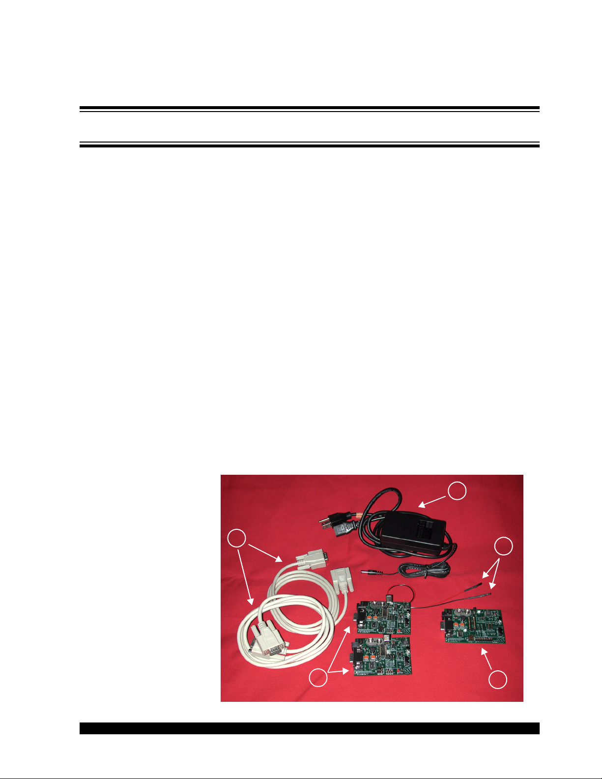
The MCP2120/MCP2150 Developer’s Kit comes with the following:
1. Two MCP2120 Developer Boards.
2. One MCP2150 Developer Board.
3. Two serial cables.
4. One 9V power supply, with power cord.
5. One pair 18” (45 cm) power jumper cables.
6. Sample kit (one MCP2120 device and one MCP2150 device)–Not
shown.
7. MCP2120/MCP2150 Developer’s Kit User’s Guide (This document)–Not
shown.
If you are missing any part of the kit, please contact your nearest Microchip
sales office listed in the back of this publication for help.
Figure 1.1: MCP2120/MCP2150 Developer’s Kit
4
3
3
5
4
2
1
1
2001 Microchip Technology Inc. DS51246A-page 1
2

MCP2120/MCP2150 USER’S GUIDE
1.2 MCP2120/MCP2150 Developer’s Kit User’s Guide
This document describes the MCP2120/MCP2150 Developer’s Kit and
tutorials, giving the user a brief overview of Microchip’s MCP2120 and
MCP2150 family of infrared communication products. Detailed information on
the individual device may be found in the device’s respective data sheet.
Detailed information on the PICDEM 2 development board may be found in
the PICDEM 2 User’s Guide (DS30374).
Chapter 1: Introduction – This chapter introduces the MCP2120/MCP2150
Developer’s Kit, lists the components in the kit, and lists related
documentation.
Chapter 2: Getting Started – This chapter gives an overview of the MCP2120
and MCP2150 Developer’s Boards, the hardware features of each
Developer’s Board, the system configurations that can be used to
demonstrate the MCP2120 and MCP2150 devices, and the PC requirements.
Chapter 3: MCP2120 Tutorial – This chapter provides a detailed description
of the steps to get the MCP2120 Developer’s board operating. These steps
include the configuration of the Developer’s boards and the Terminal
Emulation program (Hyperterminal) used on the PC.
Chapter 4: MCP2150 Tutorial – This chapter provides a detailed description
of the steps to get the MCP2150 Developer’s board operating. These steps
include the configuration of the Developer’s boards, the Terminal Emulation
program (Hyperterminal) used on the PC, and the installation and
configuration of the PC IrDA standard drivers.
Chapter 5: Using PICDEM 1 or PICDEM 2 Board as Host. This chapter
discusses the use of the PICDEM boards as a demonstration platform as a
Host Controller for an MCP2120 Developer’s Board or an MCP2150
Developer’s Board. This chapter makes reference to Application Notes which
contain demonstration code.
Appendix A: Hardware Description: This appendix describes in detail the
hardware of the MCP2120 Developer’s board and MCP2150 Developer’s
board. This includes the component layout of each board (silkscreen) and the
schematic of each board.
Revision History: This covers the major changes to the document between
the revisions.
Index: This lists the pages where major topics are located.
DS51246A-page 2 2001 Microchip Technology Inc.

1.3 Sample Devices
Each kit comes with one MCP2120 device and one MCP2150 device. This
allows a prototype system to be developed that can be used with an
MCP2120 Developer’s Board or an MCP2150 Developer’s Board.
1.4 Reference Documents
Reference documents may be obtained by contacting your nearest Microchip
sales office (listed in the back of this document) or by downloading via the
Microchip website (www.microchip.com).
• MCP2120 Data Sheet, DS21618
• MCP2150 Data Sheet, DS21655
• AN756, “Using the MCP2120 for Infrared Communication”, DS00756
• AN758,
tivity”, DS00758
• TB046, “Connecting the MCP2150 to the Psion Operating System”,
DS91046
• TB047,
tem”
• TB048, “Connecting the MCP2150 to the Windows
tem”, DS91048
“Using the MCP2150 to Add IrDA
“Connecting the MCP2150 to the Windows
, DS91047
Introduction
®
Standard Wireless Connec-
®
CE Operating Sys-
®
Operating Sys-
• TB049, “Connecting the MCP2150 to the Palm™ Operating System”,
DS91049
1.5 Other Related Documents
• MPASM User’s Guide with MPLINK™ Linker and MPLIB™ Library,
DS33014
•PRO MATE
•PICSTART
• MPLAB
• MPLAB
• Microchip’s Third Party Guide, DS00104
IrDA is a registered trademark of the Infrared Data Association.
®
II User’s Guide, DS30082
®
Plus User’s Guide, DS51028
®
ICE User’s Guide, DS51159
®
ICD User’s Guide, DS51184
2001 Microchip Technology Inc. DS51246A-page 3

MCP2120/MCP2150 USER’S GUIDE
NOTES:
DS51246A-page 4 2001 Microchip Technology Inc.

MCP2120/MCP2150
12
Chapter 2. Getting Started
2.1 Introduction
This chapter covers an overview of the MCP2120 and MCP2150 Developer’s
Boards features, the system configurations that they can be used in, and the
system requirements for the tutorials.
2.2 Highlights
Topics covered in this chapter
USER’S GUIDE
• MCP2120 Developer’s Board
• MCP2150 Developer’s Board
• System Configurations
• PC Requirements
2001 Microchip Technology Inc. DS51246A-page 5

MCP2120/MCP2150 USER’S GUIDE
2.3 Developer Board Features
2.3.1. MCP2120 Developer’s Board
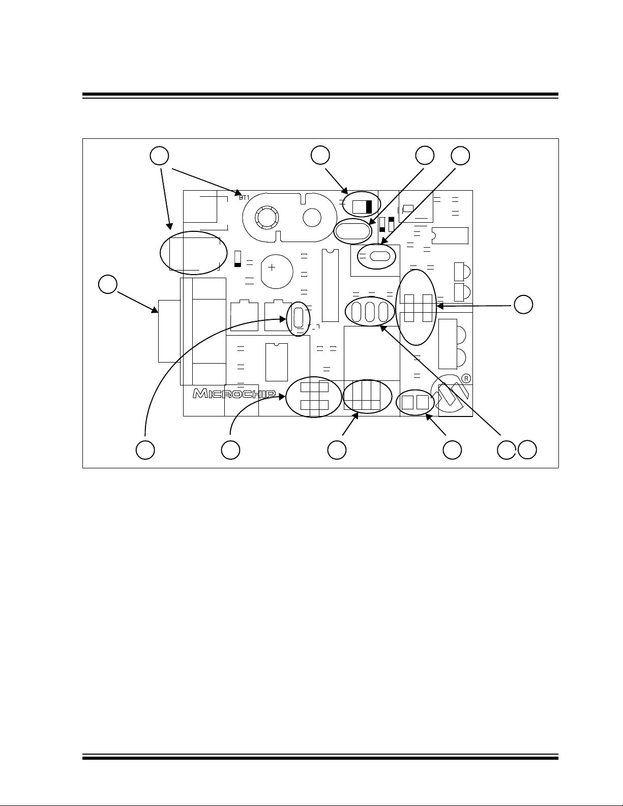
The MCP2120 Developer’s Board, as shown in Figure 2.1, has the following
hardware features:
1. On-board +5V regulator for direct input from 9V, 750 mA AC/DC wall
adapter or 9V battery.
2. Hooks for a +5V, 750 mA regulated DC supply.
3. DB-9 connector and associated hardware for direct connection to
MCP2120 UART (DB-9 interface requires RS-232 signal levels).
4. Four-pin header connection to UART interface (Header requires TTL
level signals).
5. Two jumpers to select source of UART signals. Either DB-9 connector or
the four-pin header.
6. Three jumpers to select desired baud rate.
7. Green power-on indicator LED.
8. Two IR Transceiver options (two jumpers select transceiver).
9. Jumper to disable MCP2120 device operation.
10. Hardware and Software Baud selection.
11. Jumper for Software Baud control when using RS-232C interface.
12. Socketed crystal.
Note: A schematic of the MCP2120 Developer’s Board is shown in
Figure A.5
DS51246A-page 6 2001 Microchip Technology Inc.
Getting Started
Figure 2.1: MCP2120 Developer’s Board Hardware
JP5
R14
DB9
C4
C7
C8
J4
J1
7
R1
Q1
R2 C2
R9 D3
Y1
U3
C3
Header
JP3:JP1
000=F
001=F
010=F
011=F
100=F
111=S/W Baud
Open=0
D6 D2
JP4
R4
(MCP2120)
Open=Enabled
R8 R7 R6
/768
OSC
/384
OSC
/192
OSC
/128
OSC
/64
OSC
RXTXMODE
RTS
J3
45 6
1
U5
J5
D4
3
C13
C9
C5
C1
J2
MCP2120 Developer’s Board
02-01608 Rev. 1
C15
C12
CR1
C14
U1
11
U2
C17
C6
R3
C10
Component
Transceiver
J6
Integrated
Transceiver
R13
C16
GND
+5V
12
U4
R5
9
C11
R15
C18
R11R10
D1
D5
J7
R12
8
U6
2
10
2001 Microchip Technology Inc. DS51246A-page 7
MCP2120/MCP2150 USER’S GUIDE
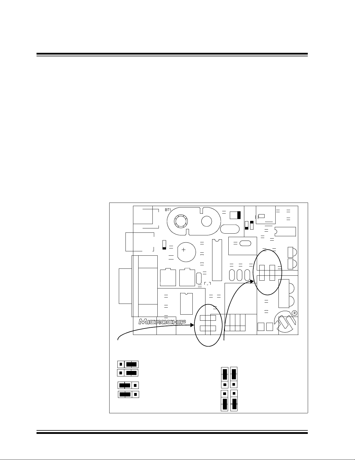
2.3.1.1 Selecting UART Source and Optical Transceiver
Interface
Figure 2.2 shows two pairs of jumpers used to route signals to and from the
MCP2120.
Jumpers J1 and J4 are used to determine the source of the signals used by
the UART interface. When the header has the pins closest to the “DB9” label
jumpered to the center pin, the DB9 is the source of the UART signal. When
the header has the pins closest to the “Header” label jumpered to the center
pin, the four-pin header is the source of the UART signal.
Jumpers J6 and J7 are used to determine the source and destination of the
infrared data signals used by the interface between the MCP2120 and Optical
Transceiver. When the header has the pins closest to the “Integrated
Transceiver” label jumpered to the center pin, the integrated transceiver is
used. When the header has the pins closest to the “Component Transceiver”
label jumpered to the center pin, the component transceiver logic is used.
Figure 2.2: MCP2120 Selecting Sources
U5
J5
D4
C13
C9
C5
C1
J2
MCP2120 Developer’s Board
02-01608 Rev. 1
C15
C12
CR1
C14
U1
JP5
R14
DB9
C4
C7
C8
R1
J4
J1
Q1
U3
R2 C2
C3
R9 D3
Y1
R8 R7 R6
JP3:JP1
000=F
001=F
010=F
011=F
100=F
111=S/W Baud
Open=0
RXTXMODE
Header
D6 D2
JP4
R4
(MCP2120)
Open=Enabled
OSC/768
OSC/384
OSC/192
OSC/128
/64
OSC
RTS
J3
U2
C17
C10
Component
Transceiver
J6
Integrated
Transceiver
+5V
R3
R13
C16
C11
R15
C6
GND
C18
U4
R5
R11R10
D1
D5
J7
R12
U6
These two jumpers select the
source of the Host signals.
J1 and J4
Header is source.
These two jumpers select the
optical transceiver logic. Both jumpers
should connect the same pin positions
J6 and J7
Component Transceiver
DB9 is source.
Integrated Transceiver
DS51246A-page 8 2001 Microchip Technology Inc.
Getting Started
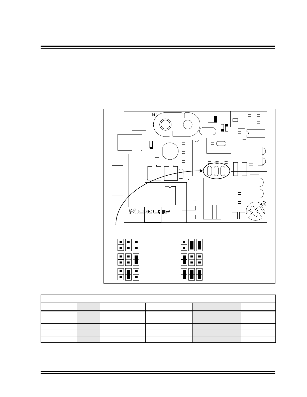
2.3.1.2 Selecting Baud Rate
Figure 2.3 shows the three Baud Rate Select Jumpers (JP3:JP1) and the
baud rate formula that is specified (baud rate dependant on MCP2120
operational frequency). Table 2.1 shows the baud rates for some crystal
frequencies.
Figure 2.3: MCP2120 Baud Rate
R15C11
C18
U4
R5
R11
D1
D5
J7
R12
U6
U5
J5
D4
C13
C9
C5
C1
J2
MCP2120 Developer’s Board
02-01608 Rev. 1
C15
C12
CR1
C14
U1
JP5
R14
C4
C7
C8
R1
Q1
U3
R2 C2
C3
J4
DB9
J1
These three jumpers select the baud rate:
JP3:JP2:JP1
JP3:JP2:JP1
R9 D3
Y1
R8 R7 R6
JP3:JP1
000=F
001=F
010=F
011=F
100=F
111=S/W Baud
Open=0
RXTXMODE
Header
D6 D2
JP4
R4
(MCP2120)
Open=Enabled
OSC/768
OSC/384
OSC/192
OSC/128
OSC/64
RTS
J3
U2
C17
C10
R10
Component
Transceiver
J6
Integrated
Transceiver
+5V
C6
R3
R13
C16
GND
F
F
F
OSC
OSC
OSC
/768
/384
/192
F
/128
OSC
F
/64
OSC
Software Baud Mode
Table: 2.1 Hardware Baud Rate Selection vs. Frequency
OSC
F
Frequency (MHz)
BAUD2:BAUD0
000
(1)
0.6144
2.000 3.6864 4.9152 7.3728 14.7456
800 2604 4800 6400 9600 19200 26042 F
001 1600 5208 9600 12800 19200 38400 52083 F
010
011
100
Note 1:
Note 2:
An external clock is recommended for frequencies below 2 MHz.
For frequencies above 7.5 MHz, the TXIR pulse width (MCP2120 Data Sheet, Electrical Specification, parameter
3200 10417 19200 25600 38400 78600 104167 F
4800 15625 28800 38400 57600 115200 156250 F
9600 31250 57600 78600 115200 230400 312500 F
IR121) will be shorter than the minimum pulse width of 1.6 µs in the IrDA standard specification.
2001 Microchip Technology Inc. DS51246A-page 9
(2)
20.000
(2)
Bit Rate
OSC
OSC
OSC
OSC
OSC
/ 768
/ 384
/ 192
/ 128
/ 64
MCP2120/MCP2150 USER’S GUIDE
2.3.1.3 UART Mode
Figure 2.4 shows the jumper which determines if the MCP2120 Developer’s
Board is to be used in Hardware Baud operation, or Software Baud operation.
When in Software Baud operation, an additional signal is required, Request
To Send (RTS), which is used to drive the RESET
of baud rate to occur.
Figure 2.4: MCP2120 UART
pin low to cause a change
U5
J5
C15
D4
C12
C13
C9
C5
C1
J2
MCP2120 Developer’s Board
02-01608 Rev. 1
CR1
C14
U1
JP5
R14
DB9
R9 D3
C4
C7
C8
R1
J4
J1
Y1
Q1
U3
JP3:JP1
000=F
C2
R2
001=F
010=F
011=F
100=F
C3
111=S/W Baud
Open=0
Header
D6 D2
JP4
R4
(MCP2120)
Open=Enabled
R8 R7 R6
OSC/768
OSC/384
OSC/192
/128
OSC
/64
OSC
RXTXMODE
RTS
C17
J3
PC UART configuration for Hardware/Software Baud mode
Hardware Baud Selection
Software Baud Selection
U2
C6
R3
C10
R10
Component
Transceiver
J6
Integrated
Transceiver
R13
C16
GND
+5V
R15C11
C18
U4
R5
R11
D1
D5
J7
R12
U6
DS51246A-page 10 2001 Microchip Technology Inc.
Getting Started
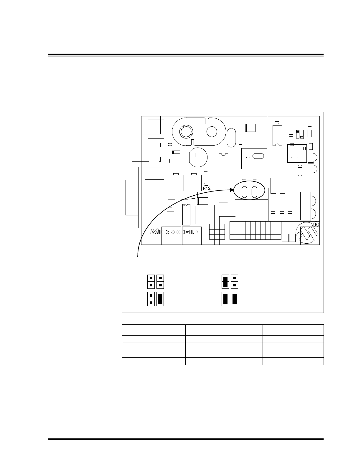
2.3.1.4 Disabling the MCP2120
Figure 2.5 shows the jumper, JP4, which will enable or disable the MCP2120
device. When the MCP2120 is disabled, the device will consume less current.
Figure 2.5: MCP2120 Enable/Disable
U5
J5
C15
D4
C12
C13
C9
C5
C1
J2
MCP2120 Developer’s Board
02-01608 Rev. 1
MCP2120 Enable/Disable
Enabled
Disabled
CR1
C14
U1
JP5
R14
R9 D3
C4
C7
C8
R1
J4
DB9
J1
Y1
Q1
U3
JP3:JP1
000=F
C2
R2
001=F
010=F
011=F
100=F
C3
111=S/W Baud
Open=0
Header
D6 D2
JP4
R4
(MCP2120)
Open=Enabled
R8 R7 R6
OSC/768
OSC/384
OSC/192
/128
OSC
/64
OSC
RXTXMODE
RTS
J3
U2
C17
C10
R10
Component
Transceiver
J6
Integrated
Transceiver
+5V
C6
R3
R13
C16
GND
R15C11
C18
U4
R5
R11
D1
D5
J7
R12
U6
In most cases, this jumper will be open. It may be closed to test system
operation when the MCP2120 is disabled. The Host Controller board may
control the operation of the MCP2120 by connecting a signal to the JP4
header as shown in Figure 2.6.
Figure 2.6: Host Controller Disabling the MCP2120
MCP2120 Developer’s Board
MCP2120
JP4
EN
2001 Microchip Technology Inc. DS51246A-page 11
Host Controller
I/O Pin
(High or Hi Impedance = Enabled
Low = Disabled)

MCP2120/MCP2150 USER’S GUIDE
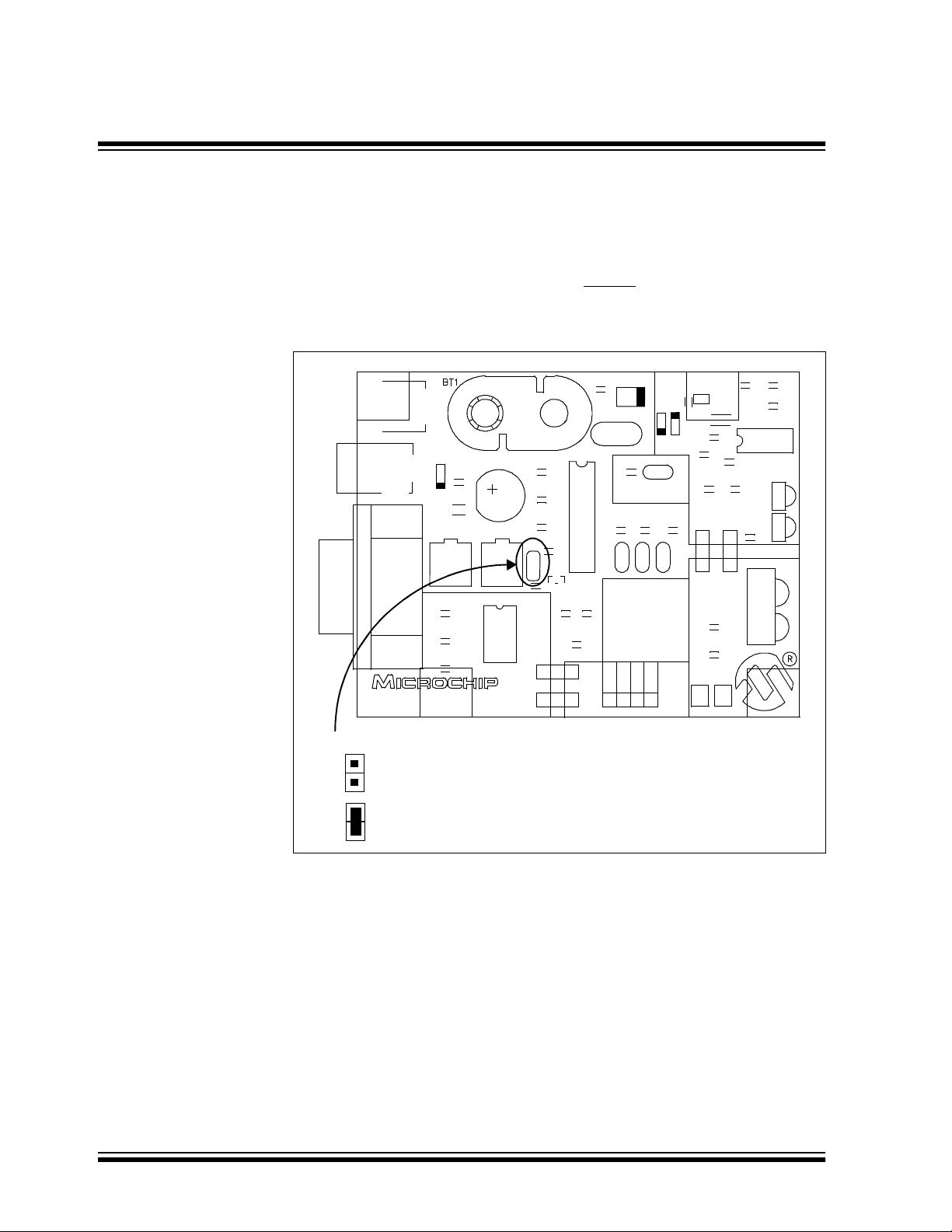
2.3.2. MCP2150 Developer’s Board
The MCP2150 Developer’s Board, as shown in Figure 2.7, has the following
hardware features:
1. On-board +5V regulator for direct input from 9V, 750 mA AC/DC wall
adapter or 9V battery.
2. Hooks for a +5V, 750 mA regulated DC supply.
3. DB-9 connector and associated hardware for direct connection to
MCP2150 UART (DB-9 interface requires RS-232 signal levels).
4. Ten-pin header connection to UART interface (Header requires TTL
level signals).
5. Three jumpers to select source of UART signals. Either DB-9 connector
or the eight-pin header.
6. Two jumpers to select desired baud rate.
7. Green power-on indicator LED.
8. Green LED for Carrier Detect.
9. Two IR Transceiver options (two jumpers select transceiver).
10. Jumper to disable MCP2150 device operation.
11. Hardware Baud selection.
Note: A schematic of the MCP2150 Developer’s Board is shown in
Figure A.6
DS51246A-page 12 2001 Microchip Technology Inc.
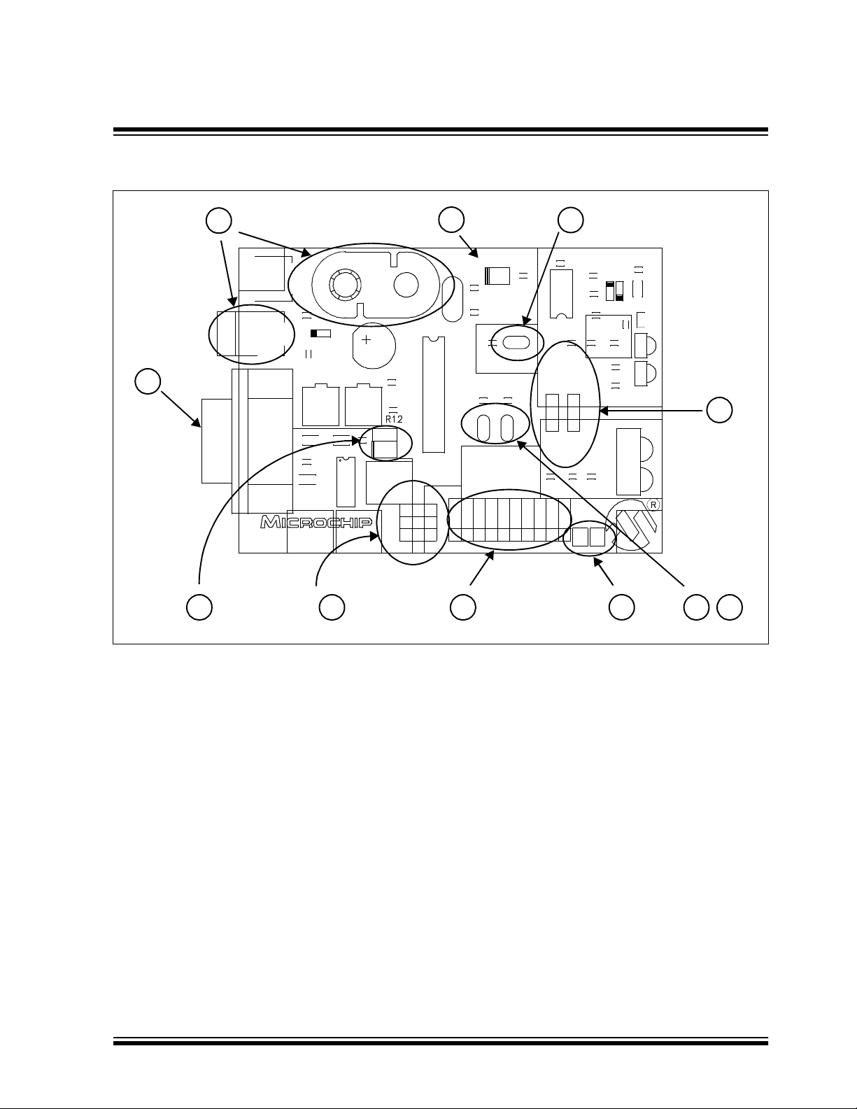
Figure 2.7: MCP2150 Board Hardware
Getting Started
U2
7
Power
Y1
Header
J1
C8
C7
Open=Enabled
JP2 JP1 BAUD
0
0
1
1
TXRXRTS
D3
JP3
R2
(MCP2150)
R4 R3
JP2 JP1
9600
0
19200
1
57600
0
115200
1
CTS
DTR
R7
DSRCDRI
45 6
1
BT1
U5
J6
3
J5
C17
D4
CR1
C14
C15
C1 C4
U1
C3
C10
MCP2150 Dev Board
02-01609 Rev. 1
C16
C2
CD
D7
C12
DB9
J4
J3
J2
8
10
C5
U4
R6 C13
R5
Component
Transceiver
J8
J7
Integrated
Transceiver
R11 C16
R13
GND
+5
+5V
R8
R9
C11
GND
D2
R14
R10
D5
U6
R1
C9
U3
C6
D1
D6
9
2
11
2001 Microchip Technology Inc. DS51246A-page 13
MCP2120/MCP2150 USER’S GUIDE
2.3.2.1 Selecting UART Source and Optical Transceiver
Interface
Figure 2.8 shows two sets of jumpers used to route signals to and from the
MCP2150.
Jumpers J2, J3 and J4 are used to determine the source of the signals used
by the UART interface. When the header has the pins closest to the “DB9”
label jumpered to the center pin, the DB9 is the source of the UART signal.
When the header has the pins closest to the “Header” label jumpered to the
center pin, the four-pin header is the source of the UART signal.
Jumpers J7 and J8 are used to determine the source and destination of the
IrDA signals used by the interface between the MCP2150 and Optical
Transceiver. When the header has the pins closest to the “Integrated
Transceiver” label jumpered to the center pin, the integrated transceiver is
used. When the header has the pins closest to the “Component Transceiver”
label jumpered to the center pin, the component transceiver logic is used.
Figure 2.8: MCP2150 Selecting Sources
BT1
U5
J6
J5
MCP2150 Dev Board
02-01609 Rev. 1
C17
D4
C14
C15
C1 C4
C3
C10
CR1
U1
C16
C2
CD
D7
DB9
C12
U2
J4
J3
J2
Y1
Header
J1
Power
C8
D3
C7
JP3
R2
(MCP2150)
Open=Enabled
R4 R3
JP2 JP1
JP2 JP1 BAUD
0
0
9600
0
1
19200
1
0
57600
1
1
115200
TXRXRTS
CTS
DTR
R7
DSRCDRI
C5
U4
R5
R6
Component
Transceiver
J8
J7
Integrated
Transceiver
R11 C16
R13
GND
+5
+5V
R8
R9
C11
D2D5
GND
C13
R14
R10
U6
C6
R1
C9
U3
D1
D6
These three jumpers select the
source of the Host signals.
J2, J3 and J4
These two jumpers select the
optical transceiver logic. Both jumpers
should connect the same pin positions
J7 and J8
Header is source.
Component Transceiver
DB9 is source.
DS51246A-page 14 2001 Microchip Technology Inc.
Integrated Transceiver
Getting Started
2.3.2.2 Selecting Baud Rate
Figure 2.9 shows the two Baud Rate Select jumpers (JP2:JP1) and the baud
rate. Table 2.2 shows the baud rates for some crystal frequencies.
Figure 2.9: MCP2150 Baud Rate
BT1
U5
J6
J5
C17
D4
CR1
C14
C15
C1 C4
C3
C10
MCP2150 Dev Board
02-01609 Rev. 1
U1
C16
C2
CD
D7
DB9
C12
Y1
U2
J4
J3
J2
Header
J1
These three jumpers select the Baud Rate
JP2:JP1
JP2:JP1
9600
Power
C8
D3
C7
JP3
R2
(MCP2150)
Open=Enabled
R4 R3
JP2 JP1
JP2 JP1 BAUD
TXRXRTS
9600
0
0
19200
1
0
57600
0
1
115200
1
1
CTS
DTR
57600
R7
DSRCDRI
C5
U4
R6 C13
R5
Component
Transceiver
J8J7
Integrated
Transceiver
R11 C16
R13
GND
+5
+5V
R8
R9
C11
GND
D2D5
R14
R10
U6
C6
R1
C9
U3
D1
D6
19200
115200
Table: 2.2 Serial Baud Rate Selection vs. Frequency
BAUD1:BAUD0 Baud Rate @ 11.0592 MHz Bit Rate
OSC
OSC
OSC
/ 1152
/ 576
/ 192
/ 96
00 9600 FOSC
01 19200 F
10 57600 F
11 115200 F
2001 Microchip Technology Inc. DS51246A-page 15
MCP2120/MCP2150 USER’S GUIDE
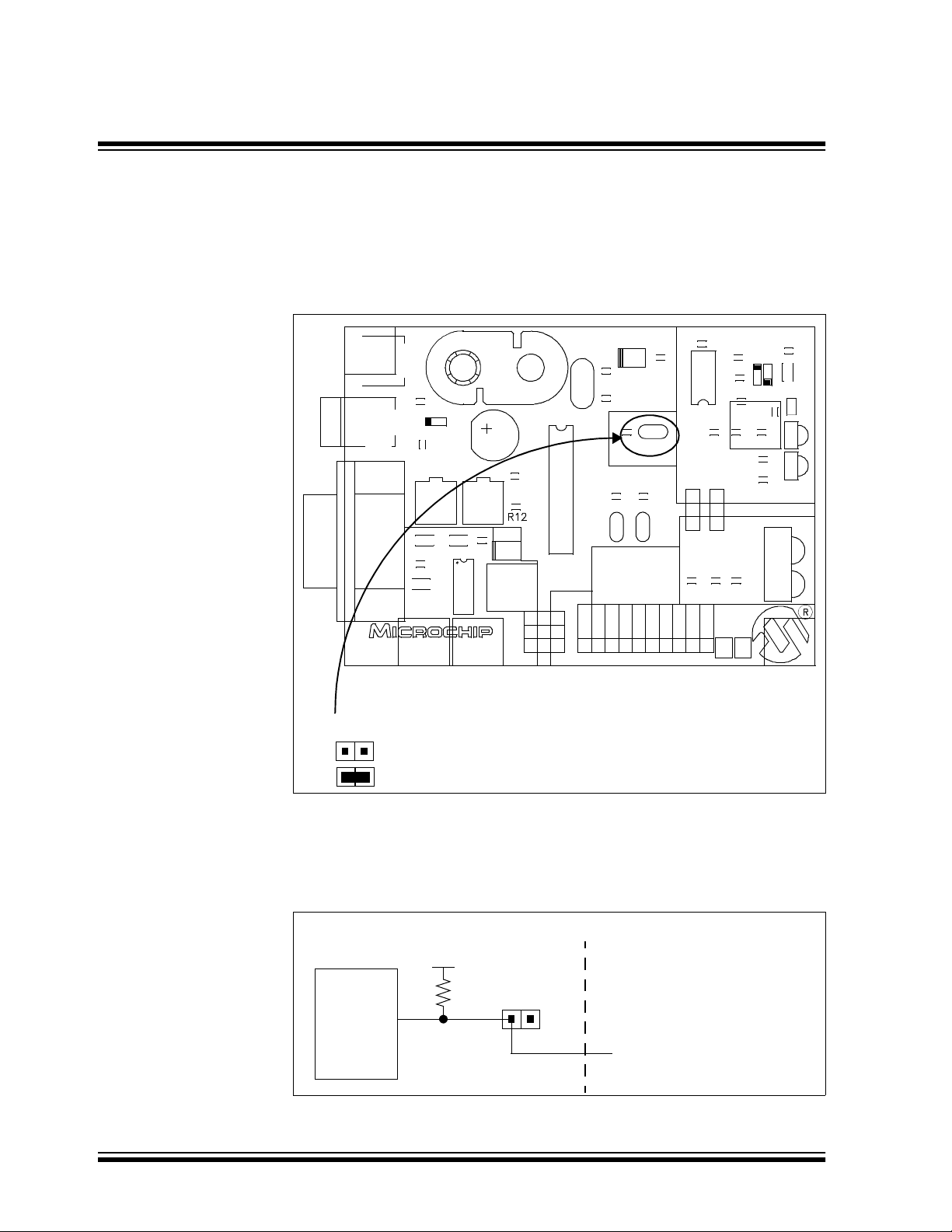
2.3.2.3 Disabling the MCP2150
Figure 2.10 shows the jumper (JP3) which will enable or disable the
MCP2150 device. When the MCP2150 is disabled, the device will consume
less current.
Figure 2.10: MCP2150 Enable/Disable
BT1
U5
J6
J5
C17
D4
CR1
C14
C15
C1 C4
C3
C10
MCP2150 Dev Board
02-01609 Rev. 1
C16
C2
U1
MCP2150 Enable/Disable
Enabled
Disabled
CD
D7
DB9
C12
R7
DSRCDRI
C5
U4
R5
R6 C13
Component
Transceiver
J8
J7
Integrated
Transceiver
R11 C16
R13
GND
+5
+5V
R8
R9
C11
Power
C8
D3
C7
Y1
U2
JP2 JP1 BAUD
J4
J3
J2
TXRXRTS
Header
J1
JP3
R2
(MCP2150)
Open=Enabled
R4 R3
JP2 JP1
9600
0
0
19200
1
0
57600
0
1
115200
1
1
CTS
DTR
D2
GND
R14
R10
D5
U6
C6
R1
C9
U3
D1
D6
In most cases, this jumper will be open. It may be closed to test system
operation when the MCP2150 is disabled. The Host Controller board may
control the operation of the MCP2150 by connecting a signal to the JP3
header as shown in Figure 2.11.
Figure 2.11: Host Controller Disabling the MCP2150
MCP2150 Developer’s Board
MCP2150
JP4
EN
DS51246A-page 16 2001 Microchip Technology Inc.
Host Controller
I/O Pin
(High or Hi Impedance = Enabled
Low = Disabled)

2.4 System Configurations
There are five configurations that one would use for initial evaluation of these
two Developer’s Boards. These configurations are:
Getting Started
Developer’s Board
1. MCP2120 Dev Board (ASCII) ↔ MCP2120 Dev Board (ASCII)
2. MCP2120 Dev Board (IR
Driver)
3. MCP2150 Dev Board (ASCII) ↔ MCP2120 Dev Board (IR Driver)
4. MCP2120 Dev Board (IR
Driver)
5. MCP2150 Dev Board (ASCII) → IrDA standard port (Palm Pilot,
The Host controller for each board can be either a Personal Computer (PC) or
another system connected to the Host header. The PC operating system (OS)
may be any desired OS that has a terminal emulation program which can
connect to the serial port and can treat the IR port as a virtual serial port. For
our tutorial, we will use the Windows 9x OS.
Note 1: Windows NT
functionality. Third Party programs exist, but are not supported or
recommended by Microsoft, so are also not recommended by
Microchip.
2: Windows
the IR port as a virtual serial port. This means that you cannot
access the IR port as a serial port. This causes issues with some
terminal emulation programs, such as Hyperterminal. Windows
2000 considers the IrDA port to be a network device. Applications
that can access a network service through a network protocol (i.e.
TCP/IP) can use the MCP2120 Developer’s Board using the appropriate Windows 2000 driver.
®
#1 Developer’s Board #2
→ MCP2120 Dev Board (IR Driver)
→ IrDA standard port (Palm™ Pilot,
cell phone, ...)
cell phone, ...)
®
4.x (and lower) does not support the IrDA standard
2000 does support the IrDA standard, but does not treat
Palm is a trademark of Palm, Inc.
Windows NT and Windows 2000 are registered trademarks of Microsoft Corporation.
2001 Microchip Technology Inc. DS51246A-page 17

MCP2120/MCP2150 USER’S GUIDE
2.4.1. Configuration 1
Developer’s Board
MCP2120 Dev Board (ASCII) ↔ MCP2120 Dev Board (ASCII)
This is the typical mode that will be used for the two MCP2120 Developer’s
Board. In this configuration, the MCP2120 board receives data as a single
ASCII byte. This byte is then translated to the IR data format, and transmitted
out of the selected optical transceiver logic.
The host interface can be from either the DB-9 (PC or other UART) or the
Header.
A PC running a terminal emulation program, such as Hyperterminal,
connected to the serial port will create this ASCII data stream. The PC can
then be connected to the Developer’s Board DB-9 connector.
2.4.2. Configuration 2
Developer’s Board
MCP2120 Dev Board (IR Driver) → MCP2120 Dev Board (IR Driver)
This is used to view the effects of the IrDA standard stack protocol on the data
stream. This can be used to better understand the construction of the IrDA
standard data packet, or as a diagnostic tool.
The host interface can be from either the DB-9 (PC or other UART) or the
Header.
#1 Developer’s Board #2
#1 Developer’s Board #2
A PC running a terminal emulation program, such as Hyperterminal,
connected to the IR port as a virtual serial port will create this ASCII data
stream. The PC can then be connected to the MCP2120 Developer’s Board
DB-9 connector.
2.4.3. Configuration 3
Developer’s Board
MCP2150 Dev Board (ASCII) ↔ MCP2120 Dev Board (IR Driver)
This is the configuration when using one MCP2120 Developer’s Board and
one MCP2150 Developer’s Board.
The MCP2150 Developer’s Board can have the host interface be from either
the DB-9 (PC or other UART) or the Header.
The MCP2120 Developer’s Board would interface to a PC running a terminal
emulation program, such as Hyperterminal, that connects the IR port to a
virtual serial port.
#1 Developer’s Board #2
DS51246A-page 18 2001 Microchip Technology Inc.

2.4.4. Configuration 4
Getting Started
Developer’s Board
MCP2120 Dev Board (IR Driver) → IrDA standard port (Palm Pilot,
This configuration is used to evaluate the MCP2120 for an IrDA system,
where the Host Controller is responsible for the IrDA protocol stack.
The MCP2120 Developer’s Board interfaces to a PC running a terminal
emulation program, such as Hyperterminal, that connects the IR port to a
virtual serial port.
2.4.5. Configuration 5
Developer’s Board
MCP2150 Dev Board (ASCII) → IrDA standard port (Palm Pilot,
This configuration is used to evaluate the MCP2150 for adding the IrDA
feature to a system. The Host controller only needs to send and receive the
required ASCII data, while the MCP2150 handles the IrDA standard protocol
stack.
The MCP2150 Developer’s Board can have the host interface be from either
the DB-9 (PC or other UART) or the Header.
#1 Developer’s Board #2
cell phone, ...)
#1 Developer’s Board #2
cell phone, ...)
2001 Microchip Technology Inc. DS51246A-page 19

MCP2120/MCP2150 USER’S GUIDE
2.5 PC Requirements
The PC used has three main requirements. These are:
1. Standard Serial Port.
2. Terminal Emulation Program.
3. IrDA standard driver installed, which treats the IR port as a virtual serial
port.
A non-legacy-free Intel compatible model with Windows 9x/2000 Operating
System (OS) would meet these requirements. The Windows OS includes a
Terminal Emulation program called Hyperterminal. Section 3.5 shows
instructions to configure Hyperterminal and demonstrate the Developer’s
Boards.
®
Note 1: Windows
the IR port as a virtual serial port. This means that you cannot
access the IR port as a serial port. This causes issues with some
terminal emulation programs, such as Hyperterminal. Windows
2000 considers the IrDA port to be a network device. Applications
that can access a network service through a network protocol (i.e.
TCP/IP) can use the MCP2120 Developer’s Board using the appropriate Windows 2000 driver.
2000 does support the IrDA standard, but does not treat
DS51246A-page 20 2001 Microchip Technology Inc.

MCP2120/MCP2150
12
Chapter 3. MCP2120 Tutorial
3.1 Introduction
This chapter covers a tutorial for using the MCP2120 Developer’s Board.
3.2 Highlights
Topics covered in this chapter
• MCP2120 Tutorial Setup
• Hardware Setup
• Setting Up the Terminal Program
• Transmitting/Receiving Data
3.3 MCP2120 Tutorial Setup
This tutorial will use both MCP2120 Developer’s Boards. The system will
operate at 9600 Baud. Each board will be connected via the UART to the
serial port of a personal computer (PC). This means that either two PCs are
required, or a PC with two serial ports, as shown in Figure 3.1. It is assumed
that two PCs will be used, and that each PC will have the Terminal Emulation
program configured identically.
USER’S GUIDE
PC
Figure 3.1: System Block Diagram
MCP2120 Developer’s
U5
J5
C15
D4
C12
C13 C14
C9
C5
C1
J2
MCP2120 Developer’s Board
02-01608 Rev. 1
Board 1
R9 D3
Y1
CR1
C4
R4
(MCP2120)
C7
Open=Enabled
C8
R8 R7 R6
R1
JP5
Q1
U3
JP3:JP1
000=Fosc/768
R14
R2C2
001=Fosc/384
010=Fosc/192
011=Fosc/128
100=Fosc/64
C3
111=S/W Baud
Open=0
U1
J4
RXTXMODE
DB9
Header
J1
C11
R15
D6D2
U2
C18
C17
C6
R3
C10
U4
JP4
R5
R11R10
Component
D1
Transceiver
D5
J7J6
R12
U6
Integrated
Transceiver
R13
C16
RTS
J3
GND
+5V
MCP2120 Developer’s
C11
R15
C18
R11 R10
Component
D1
Transceiver
D5
R12
U6
Transceiver
Board 2
C17
D6D2
U2
C6
R3
C10
U4
JP4
R5
(MCP2120)
Open=Enabled
J7 J6
Integrated
000=Fosc/768
001=Fosc/384
010=Fosc/192
R13
011=Fosc/128
100=Fosc/64
111=S/W Baud
C16
J3
GND
+5V
R4
R8R7R6
JP3:JP1
MODE
Open=0
RTS
R9D3
RX
TX
Y1
C4
C7
C8
R1
JP5
Q1
U3
R14
R2C2
C3
Header
J4
MCP2120 Developer’s Board
J1
U5
J5
CR1
C15
D4
C12
C13C14
C9
C5
C1
U1
DB9
J2
02-01608 Rev. 1
PC
2001 Microchip Technology Inc. DS51246A-page 21

MCP2120/MCP2150 USER’S GUIDE
3.4 Hardware Setup
3.4.1. Oscillator
The crystal oscillator has pin receptacles to allow the changing of the
MCP2120 oscillator frequency. For the tutorial, we will be using a crystal
frequency of 7.3728 MHz. This crystal frequency is shipped in the kit.
3.4.2. Board Jumpers
The MCP2120 and MCP2150 Developer’s Boards may use one of two host
interfaces, the DB-9 interface to connect to a PC, or the header to connect to
a controller board.
For the tutorial, the host signal will come from the DB-9 connector and the
infrared data signals will interface to the Integrated Optical Transceiver.
Figure 3.2 shows how the two 3-pin jumpers need to be connected for this
configuration.
Figure 3.2: MCP2120 Developer’s Board Component Layout
U5
J5
C15
D4
C12
C13
C9
C5
C1
J2
MCP2120 Developer’s Board
02-01608 Rev. 1
These two jumpers select the
source of the Host signals.
J1 and J4
DB9 is source.
CR1
C14
U1
JP5
R14
DB9
R9 D3
C4
C7
C8
R1
J4
J1
Y1
Q1
U3
JP3:JP1
000=F
C2
R2
001=F
010=F
011=F
100=F
C3
111=S/W Baud
Open=0
Header
D6 D2
JP4
R4
(MCP2120)
Open=Enabled
R8 R7 R6
OSC/768
OSC/384
/192
OSC
/128
OSC
/64
OSC
RXTXMODE
RTS
U2
C17
C6
R3
C10
R10
Component
Transceiver
J6
Integrated
Transceiver
R13
C16
J3
GND
+5V
R15C11
C18
U4
R5
R11
D1
D5
J7
R12
U6
These two jumpers select the
optical transceiver logic. Both jumpers
should connect the same pin positions
J6 and J7
Integrated Transceiver
DS51246A-page 22 2001 Microchip Technology Inc.

MCP2120 Tutorial
Figure 3.3 shows the three Baud Rate Select jumpers (JP3:JP1) and the baud
rate formula that is specified (baud rate dependant on MCP2120 operational
frequency). The tutorial requires these jumpers to be open for a baud rate of
9600, when the crystal frequency is 7.3728 MHz.
Figure 3.3: MCP2120 Baud Rate
C11
R15
C18
U4
R5
R11R10
D1
D5
J7
R12
U6
U5
J5
C15
D4
C12
C13 C14
C9
C5
C1
J2
MCP2120 Developer’s Board
02-01608 Rev. 1
CR1
U1
JP5
R14
R9 D3
C4
C7
C8
R1
J4
DB9
J1
Y1
Q1
U3
JP3:JP1
000=F
C2
R2
001=F
010=F
011=F
100=F
C3
111=S/W Baud
Open=0
Header
D6 D2
JP4
R4
(MCP2120)
Open=Enabled
R8 R7 R6
/768
OSC
/384
OSC
/192
OSC
/128
OSC
/64
OSC
RXTXMODE
RTS
J3
U2
C17
C10
Component
Transceiver
J6
Integrated
Transceiver
+5V
C6
R3
R13
C16
GND
These three jumpers select the Baud Rate
JP3:JP2:JP1
F
/768
OSC
2001 Microchip Technology Inc. DS51246A-page 23

MCP2120/MCP2150 USER’S GUIDE
Figure 3.4 shows jumpers JP4 and JP5 and their state. For the tutorial, both
of these jumpers are required to be open.
Figure 3.4: MCP2120 UART Mode and Enable Mode
U5
J5
D4
C13 C14
C9
C5
C1
J2
MCP2120 Developer’s Board
02-01608 Rev. 1
C15
C12
CR1
U1
JP5
R14
DB9
C4
C7
C8
R1
J4
J1
C11
R9 D3
Y1
Q1
U3
JP3:JP1
000=F
C2
R2
001=F
010=F
011=F
100=F
C3
111=S/W Baud
Open=0
Header
D6 D2
JP4
R4
(MCP2120)
Open=Enabled
R8 R7 R6
/768
OSC
/384
OSC
/192
OSC
/128
OSC
/64
OSC
RXTXMODE
RTS
U2
C17
C6
R3
C10
Component
Transceiver
J6
Integrated
Transceiver
R13
C16
J3
GND
+5V
R15
C18
U4
R5
R11R10
D1
D5
J7
R12
U6
PC UART configuration for
Hardware/Software Baud mode
Hardware Baud Selection
MCP2120 Enable/Disable
Enabled
DS51246A-page 24 2001 Microchip Technology Inc.

3.5 Setting Up the Terminal Program
Windows® 95 Operating System (OS) comes with a Terminal Emulation
program called Hyperterminal. This tutorial uses this program to demonstrate
the operation of the MCP2120/MCP2150 Developer’s Kit boards.
MCP2120 Tutorial
To open Hyperterminal, select Start > Programs > Accessories
Hyperterminal folder. Then double click the program file Hypertrm.exe. to start
Hyperterminal. Figure 3.5 shows the initial screen once the Hyperterminal
program is open. You will then need to select a name for this configuration.
Figure 3.5: Hyperterminal Opening Screen
For the initial test, we will set up the system to operate at 9600 baud. Type the
name as shown in Figure 3.6 and select any icon. Click OK.
and select the
Figure 3.6: Choosing Name and Icon
Windows is a registered trademark of Microsoft Corporation.
2001 Microchip Technology Inc. DS51246A-page 25

MCP2120/MCP2150 USER’S GUIDE
The menu in Figure 3.7 appears. You will need to select the port your serial
port is on (Connect using). In our case, we are using COM1. Click OK.
Figure 3.7: Selecting Communications (COM) Port
The Default settings for COM1 are displayed in Figure 3.8.
Figure 3.8: Hyperterminal Default COM Port Settings
DS51246A-page 26 2001 Microchip Technology Inc.

MCP2120 Tutorial
The COM port settings need to be modified so the Bits per second is “9600”
and the Flow Control is “None”, as shown in Figure 3.9. Click OK when
done.
Figure 3.9: Desired Hyperterminal COM Port Settings
2001 Microchip Technology Inc. DS51246A-page 27

MCP2120/MCP2150 USER’S GUIDE
The terminal window opens connected to the serial port as shown in
Figure 3.10.
Figure 3.10: Hyperterminal Screen After Initial Setup
DS51246A-page 28 2001 Microchip Technology Inc.

MCP2120 Tutorial
When the characteristics of the Hyperterminal session need to be modified,
the program should be disconnected from the port. To disconnect, click on the
icon with the handset with the down arrow onto the phone base as shown in
Figure 3.11.
Figure 3.11: Disconnecting Hyperterminal
2001 Microchip Technology Inc. DS51246A-page 29

MCP2120/MCP2150 USER’S GUIDE
To modify the properties of this Hyperterminal session, select
Properties
as shown in Figure 3.12.
Figure 3.12: Selecting Hyperterminal Properties Menu
File >
DS51246A-page 30 2001 Microchip Technology Inc.

MCP2120 Tutorial
The Hyperterminal Properties window will appear as shown in Figure 3.13.
Clicking the “Configure...” button will open the COM Properties window
shown in Figure 3.14.
Figure 3.13: Hyperterminal Properties Menu (Connect To)
2001 Microchip Technology Inc. DS51246A-page 31

MCP2120/MCP2150 USER’S GUIDE
Verify the settings are as desired. If not, change the settings to match the
settings in Figure 3.14. Click the OK button and you will return to the window
shown in Figure 3.13.
Figure 3.14: Configure Connection Menu
DS51246A-page 32 2001 Microchip Technology Inc.

MCP2120 Tutorial
Click on the Settings tab. Figure 3.15 shows the default settings. The
“Backscroll buffer lines” setting can be modified to 0, if desired. This will
make viewing information in the Hyperterminal window more convenient.
Figure 3.15: Hyperterminal Properties Menu (Settings)
Clicking on the “Input Translation...” button will bring up the following
window. Click Cancel to close this window.
Figure 3.16: Input Translation Menu
2001 Microchip Technology Inc. DS51246A-page 33

MCP2120/MCP2150 USER’S GUIDE
Clicking on the “ASCII Setup...” button will bring up the ASCII Setup window.
Make the changes as shown in Figure 3.17 by checking the “Echo typed
characters locally” setting. Click OK to apply these changes and close the
window.
Figure 3.17: ASCII Setup Menu
DS51246A-page 34 2001 Microchip Technology Inc.

3.6 Transmitting/Receiving Data
Now both PCs should have their Hyperterminal program running in the
connected mode with the same COM port settings. See Figure 3.9.
Each MCP2120 Developer’s Board should be powered. Use the pair of 18”
(45 cm) power jumper cables to power MCP2120 Developer’s Board #2 from
MCP2120 Developer’s Board #1. Optionally, MCP2120 Developer’s Board #2
could be powered from a 9V battery. When the MCP2120 Developer’s Board
is powered, the green LED (labeled D3) will be on.
Each MCP2120 Developer’s Board should be connected to their respective
PC serial port, so that Hyperterminal can communicate to the board.
The MCP2120 Developer’s Board should be oriented so that the integrated
optical transceivers are aligned with each other (as shown in Figure 3.18). For
the initial communication between the two boards, the MCP2120 Developer’s
Boards should be approximately 6” (15 cm) apart.
Type a string of characters in the Hyperterminal window on PC #1. This same
character sting should appear in the Hyperterminal window of PC #2. Typing a
string of characters in the Hyperterminal window on PC #2 should have the
same character string appear in the Hyperterminal window of PC #1.
Congratulations! You may now start modifying the system to evaluate/test the
operation of the MCP2120 and MCP2120 Developer’s Board.
MCP2120 Tutorial
Figure 3.18: MCP2120 Tutorial System
To IrDA Developer’s Kit Power Supply (9V)
MCP2120 Developer’s Board #1
R9 D3
D6 D2
Y1
JP3:JP1
000=Fosc/768
001=Fosc/384
010=Fosc/192
011=Fosc/128
100=Fosc/64
111=S/W Baud
Open=0
Header
R4
(MCP2120)
Open=Enabled
R8 R7 R6
RXTXMODE
C17
JP4
RTS
J3
To PC #1
U5
J5
C15
D4
C12
C13 C14
C9
C5
C1
J2
MCP2120 Developer’s Board
02-01608 Rev. 1
CR1
C4
C7
C8
R1
JP5
Q1
U3
R14
C2
R2
C3
U1
J4
DB9
J1
Pair of 18” Power Jumper Cables
U2
R3
C10
Component
Transceiver
J6
Integrated
Transceiver
R13
C16
+5V
R15C11
C18
C6
U4
R5
R11R10
D1
D5
J7
R12
U6
IR
GND
U6
MCP2120 Developer’s
+5V
GND
J3
RXTXMODE
RTS
C16
R13
R12
J7J6
D5
D1
R11R10
R5
U4
R3
C6
C18
R15
C11
Open=0
111=S/W Baud
100=Fosc/64
011=Fosc/128
010=Fosc/192
001=Fosc/384
000=Fosc/768
Transceiver
JP3:JP1
Integrat ed
R8 R7 R6
Transceiver
Component
Open=Enabled
(MCP2120)
R4
JP4
C10
C17
U2
D6 D2
Board #2
J1
Header
DB9
J4
C3
R2
C2
R14
U3
Q1
JP5
R1
C8
C7
C4
Y1
R9 D3
To PC # 2
02-01608 Re v. 1
MCP2120 Developer’s Board
U1
CR1
J2
C1
C5
C9
C13 C14
C12
D4
C15
J5
U5
2001 Microchip Technology Inc. DS51246A-page 35

MCP2120/MCP2150 USER’S GUIDE
3.6.1. System Debug Tips
If you are not getting communications between the two boards, some
debugging is in order. Here are some suggested steps:
• Verify that the Hyperterminal programs are set up correctly
• Verify that both Hyperterminal sessions are “connected”
• Verify that the MCP2120 Developer’s Boards are powered
• Verify that the MCP2120 Developer’s Boards are set up correctly
If that review does not locate the issue, then more in depth debugging is
required. These steps require an oscilloscope. A digital 4-channel
oscilloscope is recommended. By typing a data byte into Hyperterminal on the
PC, the oscilloscope can be used to determine where in the system the data
byte was “lost”.
Figure 3.19 and Figure 3.20 shows a debug flow to help troubleshoot the
communications between the two MCP2120 Developer’s Boards. Figure 3.19
shows the steps for the transmit side of System #1 (PC #1 and MCP2120
Developer’s Board #1). If it appears that the TXIR signal is correct, then the
receive side needs to be validated. Figure 3.20 shows the steps for the
receive side of System #2 (PC #2 and MCP2120 Developer’s Board #2).
These steps can then be used to debug the transmit side of System #2 and
the receive side of System #1.
DS51246A-page 36 2001 Microchip Technology Inc.

MCP2120 Tutorial
Figure 3.19: Debug Flowchart - MCP2120 Developer’s Board #1 Side
Debug Board #1
Set up digital oscilloscope to
capture waveform on first
falling edge (Start bit)
Type character in PC #1
Hyperterminal window
Data
appear on
MCP2120
TX pin?
Yes
Data
No
Problem with MCP2120
Verify device has power/ground
Ensure jumper JP4 is open
Ensure crystal oscillator is correct
frequency and operating
Ensure Baud Rate is correct
(jumpers JP1, JP2, and JP3)
Try replacing with new MCP2120
appear on
MCP2120
TXIR pin?
Yes
Goto
Debug Board #2
No
Data
appear on
MAX232
R1IN pin?
Yes
Data
appear on
MAX232
R1OUT
pin?
Yes
No
Verify that the connection from
PC #1 to Board #1 is good.
Try communication with
another serial device
(such as PICSTART Plus).
No
Verify 3 pin header J4
is jumpered correctly
2001 Microchip Technology Inc. DS51246A-page 37
It appears that the
MAX232 device
is damaged

MCP2120/MCP2150 USER’S GUIDE
Figure 3.20: Debug Flowchart - MCP2120 Developer’s Board #2 Side
Debug Board #2
Data
appear on
MCP2120
RXIR
pin?
Yes
Data
appear on
MCP2120
RX pin?
Yes
No
No
Verify that the connection for
Board #1 TXIR to Optical
Transceiver and Board #2
Optical Transceiver to RXIR
(3 pin headers J6 and J7).
Ensure that the Optical
Transceivers are aligned.
Ensure that distance between
Board #1 and Board #2 is
approximately 6” (15 cm).
Try component transceiver
option on each board
(Board #1, then Board #2,
and lastly both boards)
Problem with MCP2120
Verify device has power/ground
Ensure jumper JP4 is open
Ensure crystal oscillator is correct
frequency and operating
Ensure Baud Rate is correct
(jumpers JP1, JP2, and JP3)
Try replacing with new MCP2120
Data
appear on
MAX232
T1IN
pin?
Yes
Data
appear on
MAX232
T1OUT
pin?
Yes
Verify that the connection from
PC #1 to Board #1 is good.
Try communication with
another serial device
(such as PICSTART Plus).
No
No
Verify 3 pin header J4
is jumpered correctly
Disconnect serial cable
to ensure T1OUT is
not loaded down. If
still no data, it appears
that the MAX232 device
is damaged
DS51246A-page 38 2001 Microchip Technology Inc.

MCP2120/MCP2150
12
Chapter 4. MCP2150 Tutorial
4.1 Introduction
This chapter covers a tutorial for using the MCP2150 Developer’s Board.
4.2 Highlights
Topics covered in this chapter
• MCP2150 Tutorial
4.3 MCP2150 Tutorial
This tutorial was not available for this revision of the MCP2120/MCP2150
Developer’s Kit User’s Guide. Please check in the Development Tools section
of the Microchip web site (www.microchip.com) for revision B of the User’s
Guide. Revision B is planned to include the tutorial on using the MCP2150
Developer’s Board with an MCP2120 Developer’s Board.
Information on Microchip Development Tools can be located on the web site
by using the Navagate window and selecting Developer’s Tool Box >
Development Tools.
USER’S GUIDE
2001 Microchip Technology Inc. DS51246A-page 39

MCP2120/MCP2150 USER’S GUIDE
NOTES:
DS51246A-page 40 2001 Microchip Technology Inc.

MCP2120/MCP2150
12
USER’S GUIDE
Chapter 5. Using a PICDEM™ 1 or PICDEM™ 2 Board
as Host
5.1 Using the PICDEM 1 Board
The PICDEM™ 1 board may be used as the host controller in an IrDA
standard compatible system. PortB can be used to display received
J1
+9V IN
J2
characters, while any of the other ports would be used for the UART and
control signals. A PICmicro
hardware UART, or the UART functionality may be implemented in software.
Figure 5.1 shows the parts layout (silk-screen) for the PICDEM 1 board.
Figure 5.1: PICDEM 1 Parts Layout
Y2
7
RN1 RN2
R8
C3
Y1
C4
J3
C16
R4
1
R4
C1 2
PULLUP
CR1
U5
+
®
C11
C13
U4
C14
C7
C15C6
R3
PORT B
PIC17C42
C1 0
R7
S3
®
microcontroller may be selected that has a
PICDEM-I
DEMO BOARD
GND
+5V
+5V GND
R2
CH0
POT
©1993
DIRECT
+5V PWR
SUPPLY
CONNECTION
GND
+5V
GND
+5V
PIC16C54/56/58
PIC16C71/84
PIC16C55/57
S2
C2
0123456
U1
C1
R6
C8
U2
R1
C9
U3
R5
S1
RTCCMCLRRA1
C5
Note 1: U1 is for use with any 40-pin PIC17C4X device.
2: U2 is for use with any 18-pin PIC16C5X, PIC16CXXX device.
3: U3 is for use with any 28-pin PIC16C5X, PIC16CXXX device.
2001 Microchip Technology Inc. DS51246A-page 41

MCP2120/MCP2150 USER’S GUIDE
5.1.1. Application Notes
There are two Application Notes that show how to use the PICDEM 1 Board
as a Host controller.
AN756, “Using the MCP2120 for Infrared Communication”, DS00756, uses
the MCP2120 Developer’s Board and has two code examples. The first is
using a PIC16F84 with the MCP2120 Developer’s Board in Hardware Baud
mode. In this mode, only two signals need to be interfaced. The RX and TX
signal. The second code example is also using a PIC16F84 with the
MCP2120 Developer’s Board in Software Baud mode. In this mode, four
signals need to be interfaced; RX, TX, MODE, and RTS (used to reset the
MCP2120).
AN758, “Using the MCP2150 to Add IrDA Standard Wireless Connectivity”,
DS00758, uses the MCP2150 Developer’s Board and has one code example.
For this application, seven signals need to be interfaced; RX, TX, DSR, DTR,
CTS, RTS, and CD.
5.1.2. For Additional PICDEM 1 Information
Additional information can located on the Microchip web site
(www.microchip.com). Information on Microchip Development Tools can be
located by using the Navigate window and selecting
Development Tools.
Developer’s Tool Box >
The PICDEM 1 User’s Guide literature number is DS33015, and the
PICDEM 1 kit can be ordered with Part Number DM163001.
DS51246A-page 42 2001 Microchip Technology Inc.

Using a PICDEM™ 1 or PICDEM™ 2 Board as Host
5.2 Using the PICDEM 2 Board
The PICDEM™ 2 board may be used as the host controller in an IrDA
standard compatible system. PortB can be used to display received
characters, while any of the other ports would be used for the UART and
control signals. A PICmicro microcontroller may be selected that has a
hardware UART, or the UART functionality may be implemented in software.
Figure 5.2 shows the parts layout (silk-screen) for the PICDEM 2 board.
Figure 5.2: PICDEM 2 Parts Layout
U8
+9V
IN
J2
J1
J5
C16
1
C13
9V BATTERY
CR2
U5
C19
C18
R14
U3
C11
CR1
+
C17
C15C12
R8
R9
R10
R11
R12
R13
TM
C14
J7
RA0
PWR
J6 76 5432
RN2
R15
Y2
R4
C3
Y1
C5
C4
PIC16C73
U4
R2
R17
RESET
C1R1R3
PICDEM 2 DEMO BOARD
PORT B
U2 U1
C2C8
Y3
C10
C7
C6
R18
RA4
S2S1 S3
©1994
10
PIC16C64/74
RC2
C9
R7
R19
RN1
2
1
MCLR
RA0
RA1
RA2
RA3
RA4
RA5
RE0
RE1
RE2
NC
(RX)
(TX)
(SDA)
(SCL)
(OSI)
(OSO)
RN4
RN3
J4 KEYPAD
1
LCD DSPLY
J3
RB7
RB6
RB5
RB4
RB3
RB2
RB1
RB0
RD7
RD6
RD5
RD4
RD3
RD2
RD1
RD0
RC7
RC6
RC5
RC4
RC3
RC2
RC1
RC0
+5V
GND
+5V
GND
14
13
R6
R5
+5V GND+5V GND
Note 1: U2 is for use with any 28-pin PIC16CXXX or PIC18CXXX device.
2: U1 is for use with any 40-pin PIC16CXXX or PIC18CXXX device.
2001 Microchip Technology Inc. DS51246A-page 43

MCP2120/MCP2150 USER’S GUIDE
5.2.1. Application Notes
Currently there are no Application Notes that use the PICDEM 2 Board as a
Host controller. The examples shown for the PICDEM 1 board can be easily
modified to have the PICDEM 2 board operate as the Host controller.
5.2.2. For Additional PICDEM 2 Information
Additional information can located on the Microchip web site
(www.microchip.com). Information on Microchip Development Tools can be
located by using the Navagate window and selecting Developer’s Tool Box >
Development Tools.
The PICDEM 2 User’s Guide literature number is DS30374, and the
PICDEM 2 kit can be ordered with Part Number DM163002.
DS51246A-page 44 2001 Microchip Technology Inc.

MCP2120/MCP2150
12
Appendix A. Hardware Detail
The MCP2120/MCP2150 Developer’s Board hardware is intended to illustrate
the ease of use of Microchip’s infrared data communication solutions. The
Developer’s Board features the following hardware elements:
A.1 Power Supply
There are three ways to supply power to the MCP2120/MCP2150
Developer’s Board:
• A 9V battery can be plugged into BT1.
• A 9V, 750 mA unregulated AC or DC supply can be plugged into J5.
• A +5V, 750 mA regulated DC supply can be connected to the two pins
provided, labled +5V and GND. A pair of 18” (45 cm) cables are provided to allow one board to power another.
A.2 Power Indicator
USER’S GUIDE
One green LED indicates whether there is power applied to the MCP2120 and
MCP2150 Developer Boards (LED lit) or not (LED off).
A.3 RS-232 Serial Port
A.3.1 MCP2120 Developer’s Board
A MAX232 compatible level shifting IC has been provided with all necessary
hardware to support connection of an RS-232 host through the DB-9
connector. The port can be connected to a PC using a straight through cable.
Refer to the MCP2120 Data Sheet for more information.
A.3.2 MCP2150 Developer’s Board
A MAX3238E compatible level shifting IC has been provided with all
necessary hardware to support connection of a RS-232 host through the
DB-9 connector. The port can be connected to a PC using a straight through
cable. Refer to the MCP2120 Data Sheet (DS21618) for more information.
2001 Microchip Technology Inc. DS51246A-page 45

MCP2120/MCP2150 USER’S GUIDE
A.4 Jumpers
Jumpers are used to allow the Developer’s Board to be configured into the
different modes that are possible. These modes include:
• Selection of Baud Rate
• Source of Host signals
• Source of Optical Transceiver signals
• Device Enable signal for power down operation
A.4.1 MCP2120 Developer’s Board
The MCP2120 Developer’s Board has the following jumpers:
1. Two jumpers to select source of UART signals. Either RS-232C socket
or the four-pin header.
2. Three jumpers to select desired baud rate.
3. Two jumpers to select IR Transceiver options.
4. Jumper to disable device operation.
5. Jumper for Software Baud control when using RS-232C interface.
Figure A.1: MCP2120 Developer’s Board Hardware
4
R9 D3
U5
J5
D4
C13
C9
C5
C1
J2
MCP2120 Developer’s Board
02-01608 Rev. 1
5
1
C15
C12
CR1
C14
U1
JP5
R14
C4
C7
C8
R1
J4
DB9
J1
Q1
U3
R2 C2
C3
Y1
JP3:JP1
000=F
001=F
010=F
011=F
100=F
111=S/W Baud
Open=0
Header
D6 D2
JP4
R4
(MCP2120)
Open=Enabled
R8 R7 R 6
/768
OSC
/384
OSC
/192
OSC
/128
OSC
/64
OSC
RXTXMODE
RTS
J3
U2
C17
C10
R10
Component
Transceiver
J6
Integrated
Transceiver
+5V
2
C6
R3
R13
C16
GND
R15C11
C18
U4
R5
R11
D1
D5
J7
R12
3
U6
DS51246A-page 46 2001 Microchip Technology Inc.

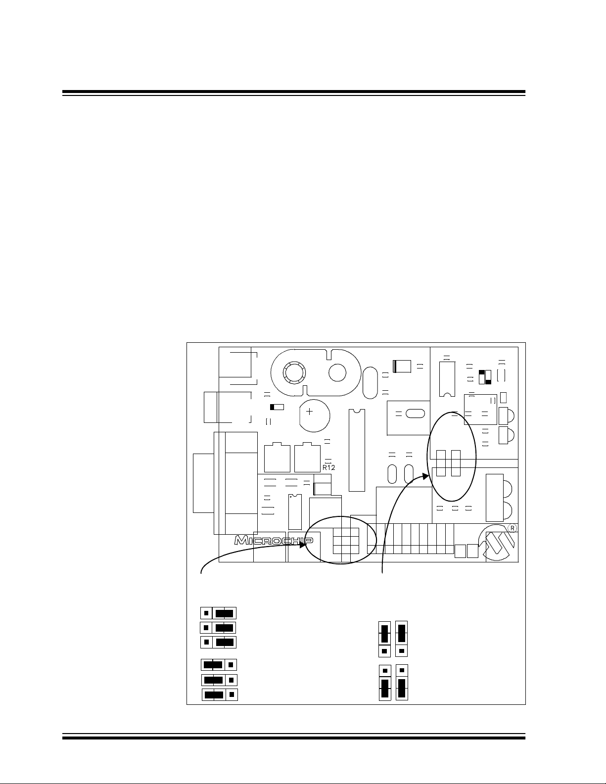
A.4.2 MCP2150 Developer’s Board
The MCP2150 Developer’s Board has the following jumpers:
1. Three jumpers to select source of UART signals. Either RS-232C socket
or the eight-pin header.
2. Two jumpers to select desired baud rate.
3. Two jumpers to select IR Transceiver options.
4. Jumper to disable device operation.
Figure A.2: MCP2150 Developer’s Board Hardware
4
Hardware Detail
BT1
U5
J6
J5
C17
D4
C14
C3
C10
MCP2150 Dev Board
02-01609 Rev. 1
CR1
C15
C1 C4
U1
1
C16
C2
CD
D7
DB9
C12
R7
DSRCDRI
C5
R8
U4
R6 C13
R5
Component
Transceiver
J8
J7
Integrated
Transceiver
R11 C16
R13
GND
+5
+5V
R9
C11
Power
C8
D3
C7
Y1
U2
JP2 JP1 BAUD
J4
J3
J2
TXRXRTS
Header
J1
JP3
R2
(MCP2150)
Open=Enabled
R4 R3
JP2 JP1
0
0
9600
0
1
19200
1
0
57600
1
1
115200
CTS
DTR
D2
GND
R14
R10
D5
U6
C6
R1
C9
U3
D1
D6
3
2
2001 Microchip Technology Inc. DS51246A-page 47

MCP2120/MCP2150 USER’S GUIDE
A.5 Oscillator Options
The MCP2120 can be operated at different frequencies, while the MCP2150
only operates at a single fixed frequency.
A.5.1 MCP2120 Developer’s Board
The MCP2120 Developer’s Board crystal has pin receptacles so that crystal
frequencies can easily be changed. Table A.1 shows the baud rates for a
given crystal frequency, based on the state of the BAUD2:BAUD0 pins.
Table A.1: Crystal Frequency / Baud Rate
OSC
F
Frequency (MHz)
MCP2120
BAUD2:BAUD0 Bit Rate
/ 768 800 2604 4800 6400 9600 19200 26042
000 F
001 F
010 F
011 F
100 F
Note 1: An external clock is recommended for frequencies below 2 MHz.
Note 2:
For frequencies above 7.5 MHz, the TXIR pulse width (
parameter IR121) will be shorter than the minimum pulse width of 1.6 µs in the IrDA standard specification.
OSC
/ 384 1600 5208 9600 12800 19200 38400 52083
OSC
/ 192 3200 10417 19200 25600 38400 78600 104167
OSC
/ 128 4800 15625 28800 38400 57600 115200 156250
OSC
/ 64 9600 31250 57600 78600 115200 230400 312500
OSC
0.6144
(1)
2.000 3.6864 4.9152 7.3728 14.7456
(2)
20.000
Data Sheet electrical specification
(2)
A.5.2 MCP2150 Developer’s Board
The MCP2150 Developer’s Board requires a fixed frequency crystal
(11.0592 MHz).
Table A.2: Crystal Frequency / Baud Rate
BAUD1:BAUD0 Bit Rate F
00 FOSC
01 F
10 F
11 F
/ 1152 9600
/ 576 19200
OSC
/ 192 57600
OSC
/ 96 115200
OSC
OSC
Frequency -
11.0592 MHz
DS51246A-page 48 2001 Microchip Technology Inc.

A.6 Board Layout
Figure A.3 shows the component layout (silkscreen) for the MCP2120 Board.
Hardware Detail
Figure A.3: MCP2120 Developer’s Board Component Layout
C11
R15
C18
U4
R5
R11R10
D1
D5
J7
R12
U6
U5
J5
C15
D4
C12
C13
C9
C5
C1
J2
MCP2120 Developer’s Board
02-01608 Rev. 1
CR1
C14
U1
JP5
R14
R9 D3
C4
C7
C8
R1
J4
DB9
J1
Y1
Q1
U3
JP3:JP1
000=F
C2
R2
001=F
010=F
011=F
100=F
C3
111=S/W Baud
Open=0
Header
D6 D2
JP4
R4
(MCP2120)
Open=Enabled
R8 R7 R6
/768
OSC
/384
OSC
/192
OSC
/128
OSC
/64
OSC
RXTXMODE
RTS
U2
C17
C6
R3
C10
Component
Transceiver
J6
Integrated
Transceiver
R13
C16
J3
GND
+5V
Figure A.4 shows the component layout (silkscreen) for the MCP2150 Board.
Figure A.4: MCP2150 Developer’s Board Component Layout
R7
DSRCDRI
C5
U4
R6 C13
R5
Component
Transceiver
J8
J7
Integrated
Transceiver
R11 C16
R13
GND
+5
+5V
R8
R9
C11
GND
D2
R14
R10
D5
U6
C6
R1
C9
U3
D1
D6
BT1
U5
C17
D4
J6
C14
C1 C4
C3
C10
J5
MCP2150 Dev Board
02-01609 Rev. 1
C15
CR1
U1
C16
C2
CD
D7
C12
DB9
Power
C8
D3
C7
U2
Y1
JP3
R2
(MCP2150)
Open=Enabled
R4 R3
JP2 JP1
JP2 JP1 BAUD
0
0
9600
0
1
19200
1
0
57600
1
1
115200
J4
J3
J2
TXRXRTS
Header
CTS
DTR
J1
2001 Microchip Technology Inc. DS51246A-page 49

MCP2120/MCP2150 USER’S GUIDE
A.7 Schematics
Figure A.5 shows the schematic for the MCP2120 Developer’s Board.
Figure A.6 shows the schematic for the MCP2150 Developer’s Board.
DS51246A-page 50 2001 Microchip Technology Inc.

Hardware Detail
Figure A.5: MCP2120 Developer’s Board Schematic
2
16
VCC
VDD
C1+
C1-4C2+5C2-
1
3
7
14
T1OUT
T2OUT
T2IN11T1IN12R1OUT
10
6
8
13
VEE
R1IN
R2IN
GND
R2OUT
9
15
2001 Microchip Technology Inc. DS51246A-page 51

MCP2120/MCP2150 USER’S GUIDE
Figure A.6: MCP2150 Developer’s Board Schematic
ORCE_OFF
F
14
15
NVALID
I
FORCEON
13
8
R1IN9R2IN
R1OUTB
16
4
11
VEE
R3IN
R3OUT
R2OUT21R1OUT
GND
2
18
20
5
10
12
26
27
VCC
VDD
C1+
28
T4OUT
T5OUT
T1OUT6T2OUT7T3OUT
T5IN
T4IN
T3IN23T2IN24T1IN
C1-
C2+
C2-
1
3
17
19
22
25
DS51246A-page 52 2001 Microchip Technology Inc.

MCP2120/MCP2150
12
Revision History
DESCRIPTION OF REVISION
This section covers the major changes to this
document between the revisions. These changes
include the corrections and enhancements that
have been implemented.
Current Revision (Revision A)
Initial release of this document
USER’S GUIDE
2001 Microchip Technology Inc. DS51246A-page 53

MCP2120/MCP2150 USER’S GUIDE
NOTES:
DS51246A-page 54 2001 Microchip Technology Inc.

MCP2120/MCP2150
12
B
Board Layout:
MCP2120 Developer’s Board Component
Layout ......................................... 49
MCP2150 Developer’s Board Component
Layout ......................................... 49
D
Disabling the MCP2120 .................................. 11
Disabling the MCP2150 .................................. 16
H
Hardware Setup:
Board Jumpers ......................................... 22
Oscillator .................................................. 22
J
Jumpers:
MCP2120 Developer’s Board .................. 46
MCP2150 Developer’s Board .................. 47
USER’S GUIDE
Index
Power Supply .................................................. 45
R
Reference Documents ...................................... 3
S
Sample Devices ................................................ 3
Schematics ..................................................... 50
Serial Port ....................................................... 45
System Configurations .................................... 17
T
Terminal Program ........................................... 25
Tutorial Setup ........................................... 21, 39
U
UART Mode .................................................... 10
M
MCP2120 Developer’s Board:
Component Transceiver ............................. 8
Disable device operation ............................ 6
Hardware Baud selection ........................... 6
Integrated Transceiver ............................... 8
Ir Transceiver ............................................. 6
Selecting Baud Rate .................................. 9
Software Baud selection ............................ 6
UART Interface .......................................... 6
MCP2150 Developer’s Board:
Component Transceiver ........................... 14
Hardware Baud selection ......................... 12
Ir Transceiver ..................................... 12, 14
Selecting Baud Rate ................................ 15
UART Interface ........................................ 12
O
Oscillator Options:
MCP2120 Developer’s Board .................. 48
MCP2150 Developer’s Board .................. 48
P
PC Requirements ........................................... 20
PICDEM 1 Board ............................................ 41
PICDEM 2 Board ............................................ 43
2001 Microchip Technology Inc. DS51246A-page 55

MCP2120/MCP2150 USER’S GUIDE
NOTES:
DS51246A-page 56 2001 Microchip Technology Inc.

NOTES:
2001 Microchip Technology Inc. DS51246A-page 57

MCP2120/MCP2150 USER’S GUIDE
NOTES:
DS51246A-page 58 2001 Microchip Technology Inc.

MCP2120/MCP2150 USER’S GUIDE
Information contained in this publication regarding device
applications and the like is intended through suggestion only
and may be superseded by updates. It is your responsibility to
ensure that your application meets with your specifications.
No representation or warranty is given and no liability is
assumed by Microchip Technology Incorporated with respect
to the accuracy or use of such information, or infringement of
patents or other intellectual property rights arising from such
use or otherwise. Use of Microchip’s products as critical components in life support systems is not authorized except with
express written approval by Microchip. No licenses are conveyed, implicitly or otherwise, under any intellectual property
rights.
Trademarks
The Microchip name and logo, the Microchip logo, PIC, PICmicro,
PICMASTER, PICSTART, PRO MATE, K
MPLAB and The Embedded Control Solutions Company are registered trademarks of Microchip Technology Incorporated in the
U.S.A. and other countries.
Total Endurance, ICSP, In-Circuit Serial Programming, FilterLab, MXDEV, microID, FlexROM, fuzzyLAB, MPASM,
MPLINK, MPLIB, PICC, PICDEM, PICDEM.net, ICEPIC,
Migratable Memory, FanSense, ECONOMONITOR, Select
Mode and microPort are trademarks of Microchip Technology
Incorporated in the U.S.A.
Serialized Quick Term Programming (SQTP) is a service mark
of Microchip Technology Incorporated in the U.S.A.
All other trademarks mentioned herein are property of their
respective companies.
© 2001, Microchip Technology Incorporated, Printed in the
U.S.A., All Rights Reserved.
Printed on recycled paper.
EELOQ
, SEEVAL,
Microchip received QS-9000 quality system
certification for its worldwide headquarters,
design and wafer fabrication facilities in
Chandler and Tempe, Arizona in Ju ly 1999. The
Company’s quality system processes and
procedures are QS-9000 compliant for its
PICmicro
devices, Serial EEPROMs and microperipheral
products. In addition, Microchip’s quality
system for the design and manufacture of
development systems is ISO 9001 certified.
®
8-bit MCUs, KEEL
®
code hopping
OQ
2001 Microchip Technology Inc. DS51246A-page 59

M
W
ORLDWIDE SALES AND SERVICE
AMERICAS
Corporate Office
2355 West Chandler Blvd.
Chandler, AZ 85224-6199
Tel: 480-792-7200 Fax: 480-792-7277
Technical Support: 480-792-7627
Web Address: http://www.microchip.com
Rocky Mountain
2355 West Chandler Blvd.
Chandler, AZ 85224-6199
Tel: 480-792-7966 Fax: 480-792-7456
Atlanta
500 Sugar Mill Road, Suite 200B
Atlanta, GA 30350
Tel: 770-640-0034 Fax: 770-640-0307
Austin - Analog
8303 MoPac Expressway North
Suite A-201
Austin, TX 78759
Tel: 512-345-2030 Fax: 512-345-6085
Boston
2 Lan Drive, Suite 120
Westford, MA 01886
Tel: 978-692-3848 Fax: 978-692-3821
Boston - Analog
Unit A-8-1 Millbrook Tarry Condominium
97 Lowell Road
Concord, MA 01742
Tel: 978-371-6400 Fax: 978-371-0050
Chicago
333 Pierce Road, Suite 180
Itasca, IL 60143
Tel: 630-285-0071 Fax: 630-285-0075
Dallas
4570 Westgrove Drive, Suite 160
Addison, TX 75001
Tel: 972-818-7423 Fax: 972-818-2924
Dayton
Two Prestige Place, Suite 130
Miamisburg, OH 45342
Tel: 937-291-1654 Fax: 937-291-9175
Detroit
Tri-Atria Office Building
32255 Northwestern Highway, Suite 190
Farmington Hills, MI 48334
Tel: 248-538-2250 Fax: 248-538-2260
Los Angeles
18201 Von Karman, Suite 1090
Irvine, CA 92612
Tel: 949-263-1888 Fax: 949-263-1338
New York
150 Motor Parkway, Suite 202
Hauppauge, NY 11788
Tel: 631-273-5305 Fax: 631-273-5335
San Jose
Microchip Technology Inc.
2107 North First Street, Suite 590
San Jose, CA 95131
Tel: 408-436-7950 Fax: 408-436-7955
Toronto
6285 Northam Drive, Suite 108
Mississauga, Ontario L4V 1X5, Canada
Tel: 905-673-0699 Fax: 905-673-6509
ASIA/PACIFIC
Australia
Microchip Technology Australia Pty Ltd
Suite 22, 41 Rawson Street
Epping 2121, NSW
Australia
Tel: 61-2-9868-6733 Fax: 61-2-9868-6755
China - Beijing
Microchip Technology Consulting (Shanghai)
Co., Ltd., Beijing Liaison Office
Unit 915
New China Hong Kong Manhattan Bldg.
No. 6 Chaoyangmen Beidajie
Beijing, 100027, No. China
Tel: 86-10-85282100 Fax: 86-10-85282104
China - Chengdu
Microchip Technology Consulting (Shanghai)
Co., Ltd., Chengdu Liaison Office
Rm. 2401, Ming Xing Financial Tower
No. 88 TIDU Street
Chengdu 610016, China
Tel: 86-28-6766200 Fax: 86-28-6766599
China - Fuzhou
Microchip Technology Consulting (Shanghai)
Co., Ltd., Fuzhou Liaison Office
Rm. 531, North Building
Fujian Foreign Trade Center Hotel
73 Wusi Road
Fuzhou 350001, China
Tel: 86-591-7557563 Fax: 86-591-7557572
China - Shanghai
Microchip Technology Consulting (Shanghai)
Co., Ltd.
Room 701, Bldg. B
Far East International Plaza
No. 317 Xian Xia Road
Shanghai, 200051
Tel: 86-21-6275-5700 Fax: 86-21-6275-5060
China - Shenzhen
Microchip Technology Consulting (Shanghai)
Co., Ltd., Shenzhen Liaison Office
Rm. 1315, 13/F, Shenzhen Kerry Centre,
Renminnan Lu
Shenzhen 518001, China
Tel: 86-755-2350361 Fax: 86-755-2366086
Hong Kong
Microchip Technology Hongkong Ltd.
Unit 901, Tower 2, Metroplaza
223 Hing Fong Road
Kwai Fong, N.T., Hong Kong
Tel: 852-2401-1200 Fax: 852-2401-3431
India
Microchip Technology Inc.
India Liaison Office
Divyasree Chambers
1 Floor, Wing A (A3/A4)
No. 11, O’Shaugnessey Road
Bangalore, 560 025, India
Tel: 91-80-2290061 Fax: 91-80-2290062
Japan
Microchip Technology Japan K.K.
Benex S-1 6F
3-18-20, Shinyokohama
Kohoku-Ku, Yokohama-shi
Kanagawa, 222-0033, Japan
Tel: 81-45-471- 6166 Fax: 81-45-471-6122
Korea
Microchip Technology Korea
168-1, Youngbo Bldg. 3 Floor
Samsung-Dong, Kangnam-Ku
Seoul, Korea 135-882
Tel: 82-2-554-7200 Fax: 82-2-558-5934
Singapore
Microchip Technology Singapore Pte Ltd.
200 Middle Road
#07-02 Prime Centre
Singapore, 188980
Tel: 65-334-8870 Fax: 65-334-8850
Taiwan
Microchip Technology Taiwan
11F -3, No . 2 07
Tung Hua North Road
Taipei, 105, Taiwan
Tel: 886-2-2717-7175 Fax: 886-2-2545-0139
EUROPE
Denmark
Microchip Technology Denmark ApS
Regus Business Centre
Lautrup hoj 1-3
Ballerup DK-2750 Denmark
Tel: 45 4420 9895 Fax: 45 4420 9910
France
Arizona Microchip Technology SARL
Parc d’Activite du Moulin de Massy
43 Rue du Saule Trapu
Batiment A - ler Etage
91300 Massy, France
Tel: 33-1-69-53-63-20 Fax: 33-1-69-30-90-79
Germany
Arizona Microchip Technology GmbH
Gustav-Heinemann Ring 125
D-81739 Munich, Germany
Tel: 49-89-627-144 0 Fax: 49-89-627-144-44
Germany - Analog
Lochhamer Strasse 13
D-82152 Martinsried, Germany
Tel: 49-89-895650-0 Fax: 49-89-895650-22
Italy
Arizona Microchip Technology SRL
Centro Direzionale Colleoni
Palazzo Taurus 1 V. Le Colleoni 1
20041 Agrate Brianza
Milan, Italy
Tel: 39-039-65791-1 Fax: 39-039-6899883
United Kingdom
Arizona Microchip Technology Ltd.
505 Eskdale Road
Winnersh Triangle
Wokingham
Berkshire, England RG41 5TU
Tel: 44 118 921 5869 Fax: 44-118 921-5820
06/01/01
DS51246A-page 60 2001 Microchip Technology Inc.
 Loading...