

Datasheet HCS410T-I-ST, HCS410T-I-SN, HCS410T-I-P, HCS410-I-ST, HCS410-I-SN Datasheet (Microchip Technology Inc)
...Page 1
1997 Microchip Technology Inc.
Preliminary
DS40158C-page 1
M
HCS410
FEATURES
Security
• Two programmable 64-bit encoder keys
• 16/32-bit bi-directional challenge and response
using one of two keys
• 69-bit transmission length
• 32-bit unidirectional code hopping, 37-bit
nonencrypted portion
• Encoder keys are read protected
• Programmable 28/32-bit serial number
• 60/64-bit, read-protected seed for secure learning
• Three IFF encryption algorithms
• Delayed increment mechanism
• Asynchronous transponder communication
• Queuing information transmitted
Operating
• 2.0V to 6.6V operation, 13V encoder only
operation
• Three switch inputs [S2, S1, S0]—sev en functions
• Batteryless bi-directional transponder
• Selectable baud rate and code word blanking
• Automatic code word completion
• Battery low signal transmitted
• Nonvolatile synchronization
• PWM or Manchester RF encoding
• Combined transmitter, transponder operation
• Anti-collision of multiple transponders
• Passive proximity activation
• Device protected against reverse battery
• Intelligent damping for high Q LC-circuits
Other
• 37-bit nonencrypted part contains 28/32-bit serial
number, 4/0-bit function code, 1-bit battery low,
2-bit CRC, 2-bit queue
• Simple programming interface
• On-chip tunable RC oscillator ( ± 10%)
• On-chip EEPROM
• 64-bit user EEPROM in transponder mode
• Battery-low LED indication
• SQTP serialization quick-time programming
• 8-pin PDIP/SOIC/TSSOP and die
Typical Applications
• Automotive remote entry systems
• Automotive alarm systems
• Automotive immobilizers
• Gate and garage openers
• Electronic door locks (Home/Office/Hotel)
• Burglar alarm systems
• Proximity access control
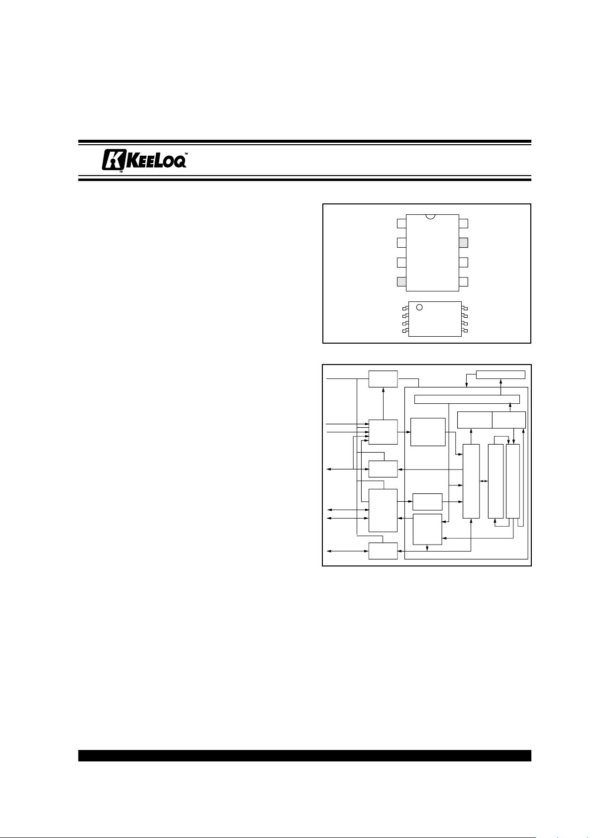
PACKA GE TYPES
BLOCK DIAGRAM
HCS410
S0
S1
S2/LED
LC1
VDD
LC0
PWM
GND
18
2
3
4
7
6
5
PDIP, SOIC
HCS410
S2/LED
LC1
GND
PWM
1
2
3
4
8
7
6
5
S1
S0
V
DD
LC0
TSSOP
Oscillator
Configuration Register
Power
Control
Wakeup
Logic
Address
Decoding
EEPROM
Debounce
Control
and
Queuer
LED
Control
PWM
Driver
PPM
Detector
PWM
PPM
Manch.
Encoder
Transponder
Circuitry
Control Logic
and Counters
Encryption/Increment
Logic
Register
VDD
S0
S1
S2
LCI0
LCI1
PWM
Code Hopping Encoder and Transponder*
K
EE
L
OQ
is a registered trademark of Microchip Technology Inc.
*Code hopping encoder patents issued in Europe, U.S.A., R.S.A.—U.S.A.: 5,517,187; Europe: 0459781
Page 2

HCS410
DS40158C-page 2
Preliminary
1997 Microchip Technology Inc.
Table of Contents
1.0 System Overview ....................................................................................................................................................3
1.1 Key Terms ........................................................................................................................................................3
1.2
K
EELOQ
Code Hopping Encoders .....................................................................................................................4
1.3 K
EE
L
OQ
IFF ......................................................................................................................................................5
2.0 Device Operation ....................................................................................................................................................6
2.1 Pinout Description ............................................................................................................................................7
2.2 Code Hopping Mode (CH Mode) .....................................................................................................................8
2.3 Code Hopping Mode Special Features ..........................................................................................................11
2.4 IFF Mode ........................................................................................................................................................14
2.5 IFF Opcodes ..................................................................................................................................................17
2.6 IFF Special Features ......................................................................................................................................18
2.7 LED Indicator .................................................................................................................................................18
3.0 EEPROM Organization and Configuration ............................................................................................................19
3.1 Encoder Key 1 and 2 .....................................................................................................................................19
3.2 Discrimination Value and Overflow ................................................................................................................19
3.3 16-bit Synchronization Counter ......................................................................................................................19
3.4 60/64-bit Seed Word/Transport Code ............................................................................................................20
3.5 Encoder Serial Number ..................................................................................................................................20
3.6 User Data .......................................................................................................................................................20
3.7 Configuration Data .........................................................................................................................................21
4.0 Integrating the HCS410 into a System ..................................................................................................................23
4.1 Key Generation ..............................................................................................................................................23
4.2 Learning an HCS410 to a Receiver ...............................................................................................................24
4.3 CH Mode Decoder Operation ........................................................................................................................25
4.4 IFF Decoder Operation ..................................................................................................................................27
5.0 Electrical Characteristics .......................................................................................................................................28
HCS410 Product Identification System ........................................................................................................................35
Page 3

HCS410
1997 Microchip Technology Inc.
Preliminary
DS40158C-page 3
DESCRIPTION
The HCS410 is a code hopping transponder device
designed for secure entry systems. The HCS410 utilizes the patented K
EELOQ
code hopping system and
bi-directional challenge-and-response for logical and
physical access control. High security learning mechanisms make this a turnkey solution when used with the
K
EELOQ
decoders. The encoder keys and synchronization information are stored in protected on-chip
EEPROM.
A low cost batteryless transponder can be implemented with the addition of an inductor and two capacitors. A packaged module including the inductor and
capacitor will also be offered.
A single HCS410 can be used as an encoder for
Remote Keyless Entry (RKE) and a transponder for
immobilization in the same circuit and thereby dramatically reducing the cost of hybrid transmitter/transponder circuits.
1.0 SYSTEM OVERVIEW
1.1 Key Terms
• Anticollision
– Allows two transponders to be in
the files simultaneously and be verified individually.
• CH Mode
– Code Hopping Mode. The HCS410
transmits a 69-bit transmission each time it is activated, with at least 32-bits changing each time the
encoder is activated.
•E
ncoder Key – A unique 64-bit k ey gener ated and
programmed into the encoder during the manufacturing process. The encoder key controls the
encryption algorithm and is stored in EEPROM on
the encoder device.
• IFF
– Identify friend or foe is a means of validating
a token. A decoder sends a random challenge to
the token and checks that the response of the
token is a valid response.
•K
EE
L
OQ
Encr
yption Algorithm – The high security
level of the HCS410 is based on the patented
K
EE
L
OQ
technology. A block cipher encryption
algorithm based on a block length of 32 bits and a
key length of 64 bits is used. The algorithm
obscures the information in such a way that even
if the unencrypted/challenge information differs by
only one bit from the information in the previous
transmission/challenge, the next coded transmission/response will be totally different. Statistically,
if only one bit in the 32-bit string of information
changes, approximately 50 percent of the coded
transmission will change.
•L
earn – The HCS product family f acilitates sev eral
learning strategies to be implemented on the
decoder. The following are examples of what can
be done.
Normal Learn –The receiver uses the same infor-
mation that is transmitted during normal operation to
derive the transmitter’s encoder key, decrypt the discrimination value and the synchronization counter.
Secure Learn* – The transmitter is activ ated through
a special button combination to transmit a stored
60-bit value (random seed) that can be used for key
generation or be part of the key. Transmission of the
random seed can be disabled after learning is completed.
•M
anufacturer’s Code – A 64-bit word, unique to
each manufacturer, used to produce a unique
encoder key in each transmitter (encoder).
•P
assive Proximity Activ ation – When the HCS410
is brought into in a magnetic field without a
command given by the base station, the HCS410
can be programmed to give an RF transmission.
•T
ransport Code – A 32-bit transport code needs
to be given before the HCS410 can be inductiv ely
programmed. This prevents accidental
programming of the HCS410.
*Secure Learn patent pending.
Page 4
HCS410
DS40158C-page 4
Preliminary
1997 Microchip Technology Inc.
1.2 K
EE
L
OQ
Code Hopping Encoders
When the HCS410 is used as a code hopping encoder
device, it is ideally suited to keyless entry systems,
primarily for vehicles and home garage door openers.
It is meant to be a cost-effective, yet secure solution to
such systems. The encoder portion of a keyless entry
system is meant to be carried by the user and operated
to gain access to a vehicle or restricted area.
Most keyless entry systems transmit the same code
from a transmitter every time a button is pushed. The
relative number of code combinations for a low end
system is also a relatively small number. These
shortcomings provide the means for a sophisticated
thief to create a device that ‘grabs’ a transmission and
retransmits it later or a device that scans all possible
combinations until the correct one is found.
The HCS410 employs the K
EE
L
OQ
code hopping technology and an encryption algorithm to achieve a high
level of security. Code hopping is a method by which
the code transmitted from the transmitter to the
receiver is different every time a button is pushed. This
method, coupled with a transmission length of 69 bits,
virtually eliminates the use of code ‘grabbing’ or code
‘scanning’.
The HCS410 has a small EEPROM array which must
be loaded with several parameters before use. The
most important of these values are:
• A 28/32-bit serial number which is meant to be
unique for every encoder
• 64-bit seed value
• A 64-bit encoder key that is generated at the time
of production
• A 16-bit synchronization counter value.
• Configuration options
The 16-bit synchronization counter value is the basis
for the transmitted code changing for each transmission, and is updated each time a button is pressed.
Because of the complexity of the code hopping encryption algorithm, a change in one bit of the synchronization counter value will result in a large change in the
actual transmitted code.
Once the encoder detects that a button has been
pressed, the encoder reads the button and updates the
synchronization counter. The synchronization counter
value, the function bits, and the discrimination value are
then combined with the encoder key in the encryption
algorithm, and the output is 32 bits of encrypted information (Figure 1-1). The code hopping portion provides up to four billion changing code combinations.
This data will change with every button press, hence, it
is referred to as the code hopping portion of the code
word.
The 32-bit code hopping portion is combined with the
button information and the serial number to form the
code word transmitted to the receiver. The code word
format is explained in detail in Section 2.2.
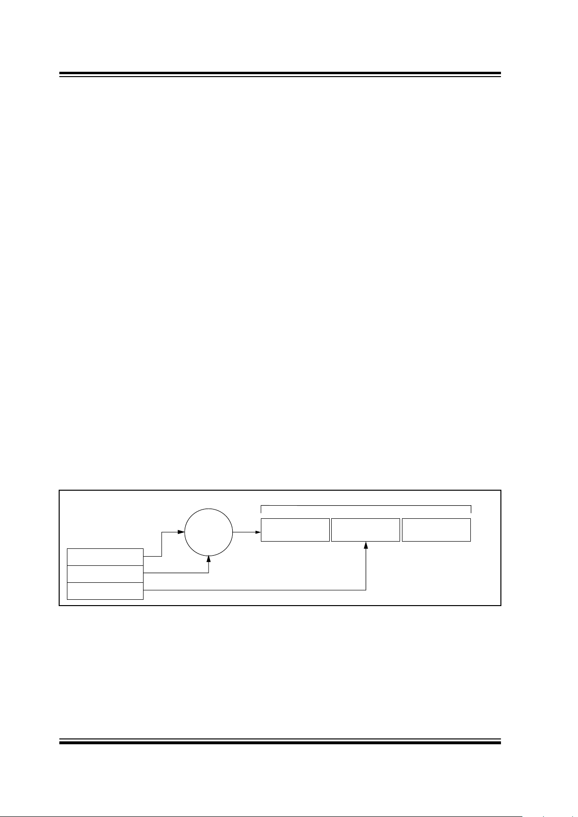
FIGURE 1-1: BASIC OPERATION OF A CODE HOPPING TRANSMITTER (ENCODER)
KEELOQ
Algorithm
Button Press
Information
Encryption
EEPROM Array
32 Bits of
Encrypted Data
Serial Number
Transmitted Information
Encoder Key
Sync Counter
Serial Number
Page 5
HCS410
1997 Microchip Technology Inc.
Preliminary
DS40158C-page 5
1.3 K
EE
L
OQ
IFF
The HCS410 can be used as an IFF transponder for
verification of a token. In IFF mode the HCS410 is ideally suited for authentication of a key before disarming
a vehicle immobilizer. Once the key has been inserted
in the car’s ignition the decoder would inductively poll
the key validating it before disarming the immobilizer.
IFF validation of the token inv olves a r andom challenge
being sent by a decoder to a token. The token then generates a response to the challenge and sends this
response to the decoder (Figure 1-2). The decoder calculates an expected response using the same challenge. The expected response is compared to the
response received from the token. If the responses
match, the token is identified as a valid token and the
decoder can take appropriate action.
The HCS410 can do either 16 or 32-bit IFF. The
HCS410 has two encryption algorithms that can be
used to generate a response to a challenge. In addition
there are up to two encoder keys that can be used by
the HCS410. Typically each HCS410 will be programmed with a unique encoder key(s).
In IFF mode, the HCS410 will wait for a command from
the base station and respond to the command. The
command can either request a read/write from user
EEPROM or an IFF challenge response. A given 16 or
32-bit challenge will produce a unique 16/32-bit
response, based on the IFF key and IFF algorithm
used.
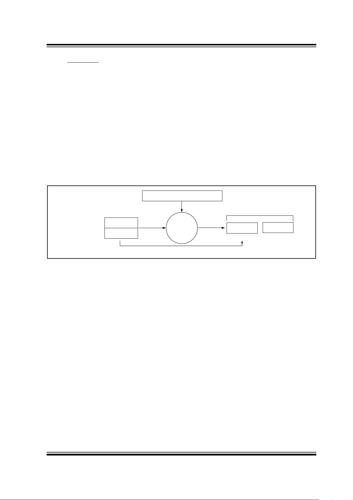
FIGURE 1-2: IBASIC OPERATION OF AN IFF TOKEN
IFF Key
Serial Number
KEELOQ
IFF
Algorithm
Serial Number
EEPROM Array
Challenge Received from Decoder
Response
Read by Decoder
Page 6
HCS410
DS40158C-page 6
Preliminary
1997 Microchip Technology Inc.
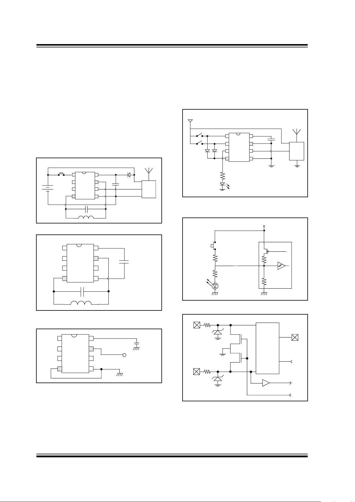
2.0 DEVICE OPERATION
The HCS410 can either operate as a normal code hopping transmitter with one or two IFF keys (Figure 2-1) or
as purely an IFF token with two IFF keys (Figure 2-2
and Figure 2-3). When used as a code hopping transmitter the HCS410 only needs the addition of buttons
and RF circuitry for use as a transmitter. Adding the
transponder function to the transmitter requires the
addition of an inductor and two capacitors as shown in
Figure 2-1 and Figure 2-2. A description of each pin is
given in Table 2-1. Table 2-2 shows the function codes
for using the HCS410.
FIGURE 2-1: COMBINED TRANSMITTER/
TRANSPONDER CIRCUIT
FIGURE 2-2: TRANSPONDER CIRCUIT
FIGURE 2-3: 2-WIRE, 1 OR 2-KEY IFF
TOKEN
Figure 2-4 shows how to use the HCS410 with a 12V
battery as a code hopping transmitter. The circuit uses
the internal regulator, normally used for charging a
capacitor/battery in LC mode, to generate a 6V supply
for the HCS410.
FIGURE 2-4: HCS410 ENCODER WITH 12V
BATTERY
FIGURE 2-5: LED CONNECTION TO
S2/LED OUTPUT
FIGURE 2-6: LC PIN BLOCK DIAGRAM
18
RF
2
3
4
7
6
5
1 µF
18
2
3
4
7
6
5
1 µF
18
2
3
4
7
6
5
1 µF
Data I/O
18
RF
2
3
4
7
6
5
6.3V
12V
Pulse
VDD
S2/LED
220Ω
220Ω
60k
30Ω
VDD
6.7V
Damp
Out
MOD
Detector
Rectifier,
Damping,
Clamping
15V
15V
100Ω
100Ω
LCI1
LCI0
Page 7
HCS410
1997 Microchip Technology Inc.
Preliminary
DS40158C-page 7
2.1 Pinout Description
The HCS410 has the same footprint as all of the other
devices in the K
EE
L
OQ
family, except for the two pins
that are reserved for transponder operations and the
LED that is now located at the same position as the S2
switch input.
• S[0:1] – are inputs with Schmitt Trigger detectors
and an internal 60k Ω (nominal) pull-down
resistors.
• S2/LED – uses the same input detection circuit as
S0/S1 but with an added PMOS transistor connected to V
DD
capable of sourcing enough current
to drive an LED.
• LC[0:1] – is the transponder interface pins to be
connected to an LC circuit for inductive communication. LC0 is connected to a detector for data
input. Data output is achieved by clamping LC0
and LC1 to GND through two NMOS transistors.
These pins are also connected to a rectifier and a
regulator, providing power to the rest of the logic
and for charging an external power source (Battery/Capacitor) through V
DD
.
TABLE 2-1: PINOUT DESCRIPTION
Name Pin Number Description
S0 1 Switch input 0
S1 2 Switch input 1
S2/LED 3 Switch input 2/LED output, Clock pin for programming mode
LC1 4 Transponder interface pin
V
SS
5 Ground reference connection
PWM 6 Pulse width modulation (PWM)
output pin/Data pin for
programming mode
LC0 7 Transponder interface pin.
V
DD
8 Positive supply voltage connection
TABLE 2-2: FUNCTION CODES
LC0 S2 S1 S0 Comments
10001Normal Code Hopping transmission
20010Normal Code Hopping transmission
30011
Delayed seed transmission if allowed by SEED and TMPSD/Normal
Code Hopping transmission
40100Normal Code Hopping transmission
50101Normal Code Hopping transmission
60110Normal Code Hopping transmission
70111
Immediate seed transmission if allowed by SEED and TMPSD/Normal
Code Hopping transmission
81000Transponder mode
Page 8
HCS410
DS40158C-page 8
Preliminary
1997 Microchip Technology Inc.
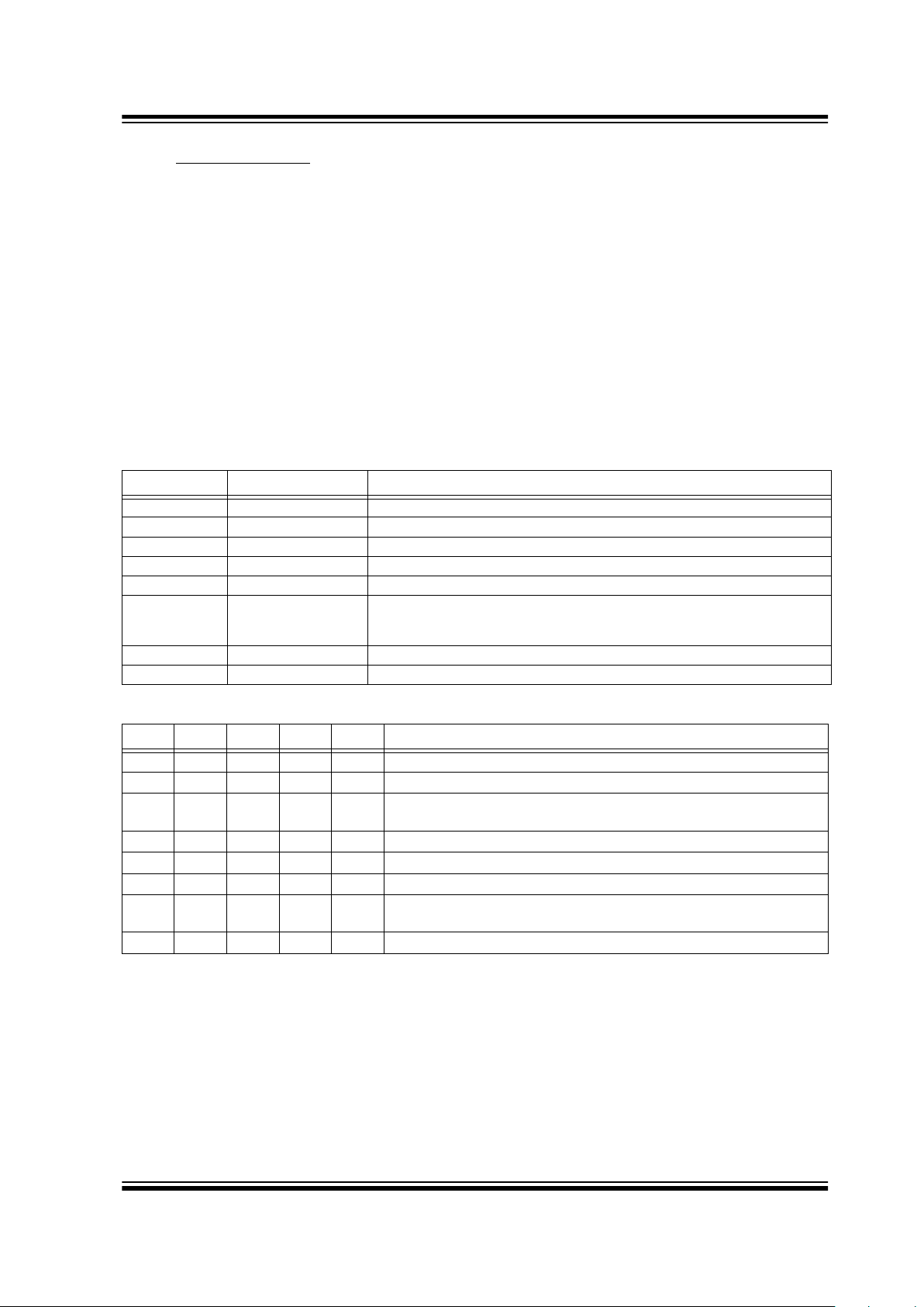
2.2 Code Hopping Mode (CH Mode)
The HCS410 wakes up upon detecting a switch closure
and then delays approximately 30 ms for switch
debounce (Figure 2-7). The synchronization counter
value, fixed information, and switch information are
encrypted to form the code hopping portion. The
encrypted or code hopping portion of the transmission
changes every time a button is pressed, even if the
same button is pushed again. Keeping a button
pressed for a long time results in the same code word
being transmitted until the button is released or timeout occurs. A code that has been transmitted will not
occur again for more than 64K transmissions. Overflow
information programmed into the encoder can be used
by the decoder to extend the number of unique transmissions to more than 192k.
If, during the transmit process, it is detected that a new
button(s) has been added, a reset will immediately be
forced and the code word will not
be completed. Please
note that buttons removed will not have any effect on
the code word unless no buttons remain pressed in
which case the current code word will be completed
and the power down will occur. If, after a button combination is pressed, and the same button combination is
pressed again within 2 seconds of the first press, the
current transmission will be aborted and a new transmission will start with the queue counter (QUE)
incremented.
FIGURE 2-7: CODE HOPPING ENCODER OPERATION
20-second
timeout
No
Transmitted
2 second
time-out
completed?
All buttons
released?
Sample Inputs
Update Sync Info
Encrypt With
T ransmit
Encoder Key
Power-up
(A button has been
pressed (Note1)
Buttons added?
Yes
Yes
Yes
No
(Note 1)
7 complete code
words?
Complete current
code word while
checking buttons
(Note 2)
Stop transmitting
DINC Set?
Power down
Buttons
pressed?
(Note 1)
Same as
previous
press?
Increment queue
counter
20 second
time-out
completed?
Buttons
pressed?
(Note 1)
Increase sync
counter
by 12
immediately
Yes
Yes
No
Yes
Yes
No
No
No
Yes
No
Yes
No
No
Note 1: 30 ms debounce on press and release of all buttons.
2: Completes a minimum of 3 code words if MTX3 is set.
No
DINC
Set?
Yes
Yes
No
Page 9
HCS410
1997 Microchip Technology Inc.
Preliminary
DS40158C-page 9
2.2.1 TRANSMISSION DATA FORMAT
The HCS410 transmission (CH Mode) is made up of
several parts (Figure 2-10 and Figure 2-11). Each
transmission is begun with a preamble and a header,
followed by the encrypted and then the fixed data. The
actual data is 69 bits which consists of 32 bits of
encrypted data and 37 bits of fixed data. Each transmission is followed by a guard period before another
transmission can begin. Refer to Table 5-4
and Table 5-5 for transmission timing specifications.
The combined encrypted and nonencrypted sections
increase the number of combinations to 1.47 x 10
20
.
The HCS410 transmits a 69-bit code word when a button is pressed. The 69-bit word is constructed from a
Fixed Code portion and Code Hopping portion
(Figure 2-8).
The Encrypted Data is generated from 4 function bits,
2 overflow bits, and 10 discrimination bits, and the 16bit synchronization counter value (Figure 2-8).
The Nonencrypted Code Data is made up of 2 QUE
bits, 2 CRC bits, a V
LOW
bit, 4 function bits, and the
28-bit serial number. If the extended serial number
(32 bits) is selected, the 4 function code bits will not be
transmitted (Figure 2-8).
FIGURE 2-8: HOP CODE WORD ORGANIZATION (RIGHT-MOST BIT IS CLOCKED OUT FIRST)
FIGURE 2-9: SEED CODE WORD ORGANIZATION
Fixed Code Data Encrypted Code Data
69 bits
of Data
Transmitted
MSB LSB
CRC
(2 bit)
VLOW
(1 bit)
Button
Status*
(4 bits)
28-bit
Serial Number
Overflow (2 bits)
bits (10 bits)
16-bit
Synchronization
CRC
(2 bits)
VLOW
(1 bit)
+
Serial Number and
Button Status (32 bits)
+ 32 bits of Encrypted Data
QUE
QUE
(Q1, Q0
S2 S1 S0 0
Button
Status
(4 bits)
S2 S1 S0 0
(2 bits)
bit)
Counter Value
Discrimination
and
* Optional.
Fixed Code Data
69 bits
of Data
Transmitted
CRC
(2 bit)
VLOW
(1 bit)
Button*
Status
(4 bits)
CRC
(2 bits)
VLOW
(1 bit)
+
QUE
QUE0
(Q1, Q0
S2 S1 S0 0
(2 bits)
bit)
Unencrypted
Button
(4 bits)
SEED
(60 bits)
+
SEED
* Optional.
Page 10
HCS410
DS40158C-page 10
Preliminary
1997 Microchip Technology Inc.
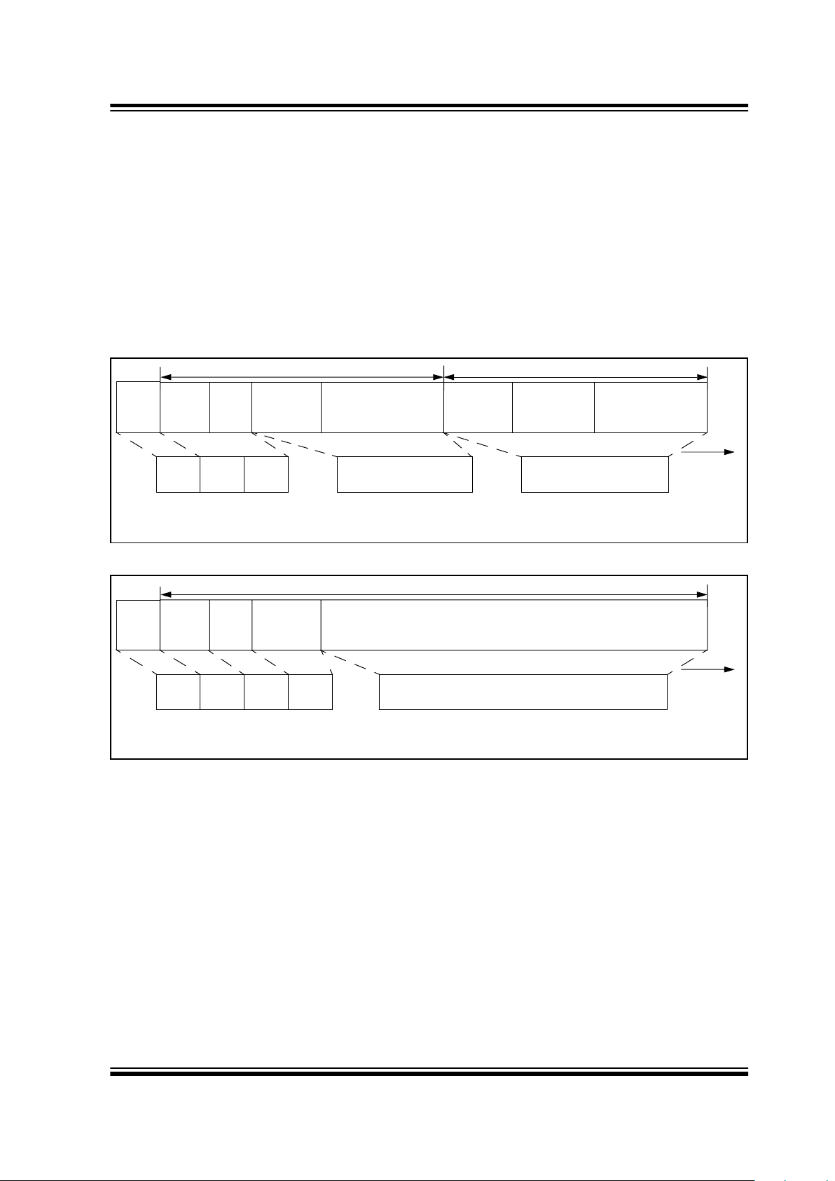
2.2.2 TRANSMISSION DATA MODULE
The Data Modulation Format is selectable between
Pulse Width Modulation (PWM) format and Manchester
encoding. Both formats are preceded by a preamble
and synchronization header, followed by the 69-bits of
data. Manchester encoding has a leading and closing
‘1’ for each code word.
The same code word is continuously sent as long as
the input pins are kept high with a guard time separating the code words. All of the timing values are in multiples of a Basic Timing Element (T
E), which can be
changed using the baud rate option bits.
FIGURE 2-10: TRANSMISSION FORMAT—MANCH = 0
FIGURE 2-11: TRANSMISSION FORMAT—MANCH = 1
LOGIC "1"
Code Word
Guard
Time
Preamble
Sync
Encrypted
TX Data
Fixed Code
BIT
LOGIC "0"
123579
46810
TE
CODE WORD:
TOTAL TRANSMISSION:
Preamble
Sync
Encrypt
Fixed
Guard
1 CODE WORD
12 456
Preamble Sync Encrypt
14 15 16
TE
Data
TE
Guard
Preamble Sync
Encrypted
Fixed Code
LOGIC "0"
123
4
BPW
CODE WORD:
TOTAL TRANSMISSION:
Sync Encrypt Fixed Guard
1 CODE WORD
12 456
Preamble Sync Encrypt
14 15 16
LOGIC "1"
Start bit
Stop bit
CODE WORD
Preamble
Time
Data
Data
Page 11
HCS410
1997 Microchip Technology Inc. Preliminary DS40158C-page 11
2.3 Code Hopping Mode Special Features
2.3.1 CODE WORD COMPLETION
Code word completion is an automatic feature that
ensures that the entire code word is transmitted, even
if the button is released before the transmission is complete. The HCS410 encoder powers itself up when a
button is pushed and powers itself down after the command is finished (Figure 2-7). If MTX3 is set in the configuration word, a minimum of three transmissions will
be transmitted when the HCS410 is activated, even if
the buttons are released.
If less than seven words have been transmitted when
the buttons are released, the HCS410 will complete the
current word. If more than seven words have been
transmitted, and the button is released, the PWM output is immediately switched off.
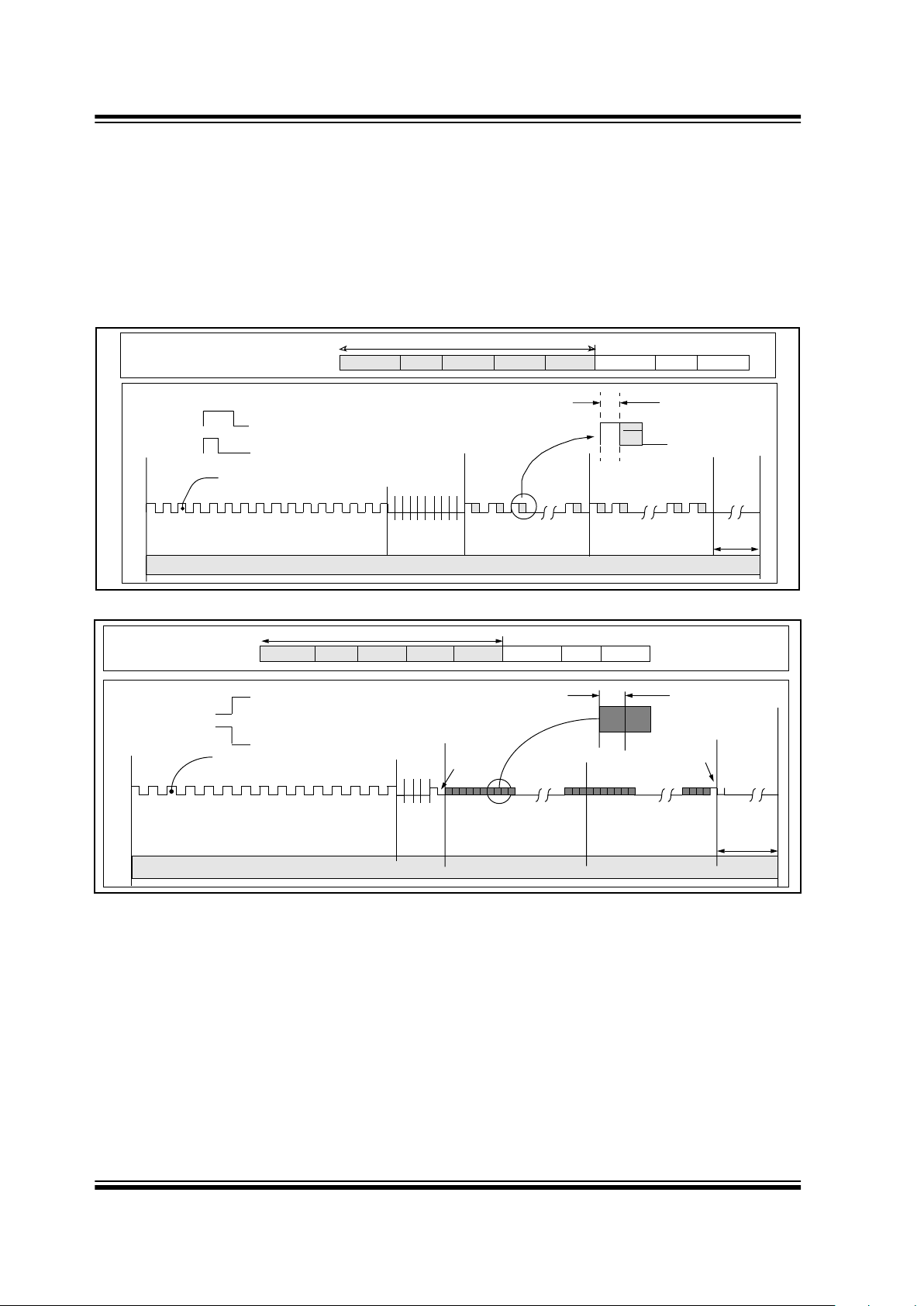
2.3.2 CODE WORD BLANKING ENABLE
Federal Communications Commission (FCC) part 15
rules specify the limits on fundamental power and
harmonics that can be transmitted. Power is calculated
on the worst case average power transmitted in a
100ms window. It is therefore advantageous to
minimize the duty cycle of the transmitted word. This
can be achieved by minimizing the duty cycle of the
individual bits and by blanking out consecutive words.
Code Word Blanking Enable (CWBE) is used for
reducing the average power of a transmission
(Figure 2-12). Using the CWBE allows the user to
transmit a higher amplitude transmission if the
transmission length is shorter. The FCC puts
constraints on the average power that can be
transmitted by a device, and CWBE eff ectively pre vents
continuous transmission by only allowing the transmission of every second or fourth word. This reduces the
average power transmitted and hence, assists in FCC
approval of a transmitter device.
The HCS410 will either transmit all code words, 1 in 2
or 1 in 4 code words, depending on the baud rate
selected and the code word blanking option. See
Section 3.7 for additional details.
2.3.3 CRC (CYCLE REDUNDANCY CHECK) BITS
The CRC bits are calculated on the 65 previously trans-
mitted bits. The CRC bits can be used by the receiver
to check the data integrity before processing starts. The
CRC can detect all single bit and 66% of double bit
errors. The CRC is computed as follows:
EQUATION 2-1: CRC CALCULATION
and
with
and Di
n
the nth transmission bit 0 ≤ n ≤ 64
FIGURE 2-12: CODE WORD BLANKING ENABLE
CRC 1[]
n 1+
CRC 0[]nDin⊕=
CRC 0[]
n 1+
CRC 0[]nDin⊕()CRC 1[]
n
⊕=
CRC 10,[]
0
0=
One Code Word
CWBE Disabled
(All words transmitted)
CWBE Enabled
(1 out of 2 transmitted)
A
2A
Amplitude
CWBE Enabled
(1 out of 4 transmitted)
4A
Time
Page 12

HCS410
DS40158C-page 12 Preliminary 1997 Microchip Technology Inc.
2.3.4 SEED T R ANSMISSION
In order to increase the level of security in a system, it
is possible for the receiver to implement what is known
as a secure learning function. This can be done by utilizing the seed value on the HCS410 which is stored in
EEPROM. Instead of the normal key generation
method being used to create the encoder key, this seed
value is used and there should not be any mathematical relationship between serial numbers and seeds for
the best security. See Section 3.7.3 for additional
details.
2.3.5 PASSIVE PROXIMITY ACTIVATION
If the HCS410 is brought into a magnetic field it enters
IFF mode. In this mode it sends out ACK pulses on the
LC lines. If the HCS410 doesn't receive any response
to the first set of ack pulses within 50 ms the HCS410
will transmit a normal code hopping transmission for 2
seconds if XPRF is set in the configuration word. The
function code during this transmission is S2:S0 = 000.
2.3.6 AUTO-SHUTOFF
The Auto-shutoff function automatically stops the
device from transmitting if a button inadvertently gets
pressed for a long period of time. This will prevent the
device from draining the battery if a button gets
pressed while the transmitter is in a pocket or purse.
Time-out period is approximately 20 seconds.
2.3.7 V
LOW: VOLTAGE LOW INDICATOR
The V
LOW bit is transmitted with every transmission
(Figure 2-8). V
LOW is set when the operating voltage
has dropped below the low voltage trip point, approximately 2.2V or 4.4V selectable at 25°C. This V
LOW sig-
nal is transmitted so the receiver can give an indication
to the user that the transmitter battery is low.
2.3.8 QUE0:QUE1: QUEUING INFORMATION
If a button is pressed, released for more than 30 ms,
and pressed again within 2 seconds of the first press,
the QUE counter is incremented (Figure 2-7). The
transmission that the HCS410 is busy with is aborted
and a new transmission is begun with the new QUE bits
set. These bits can be used by the decoder to perform
secondary functions using only a single button without
the requirement that the decoder receive more than
one completed transmission. F or example if none of the
QUE bits are set the decoder only unlocks the driver’s
door, if QUE0 is set (double press on the transmitter)
the decoder unlocks all the doors.
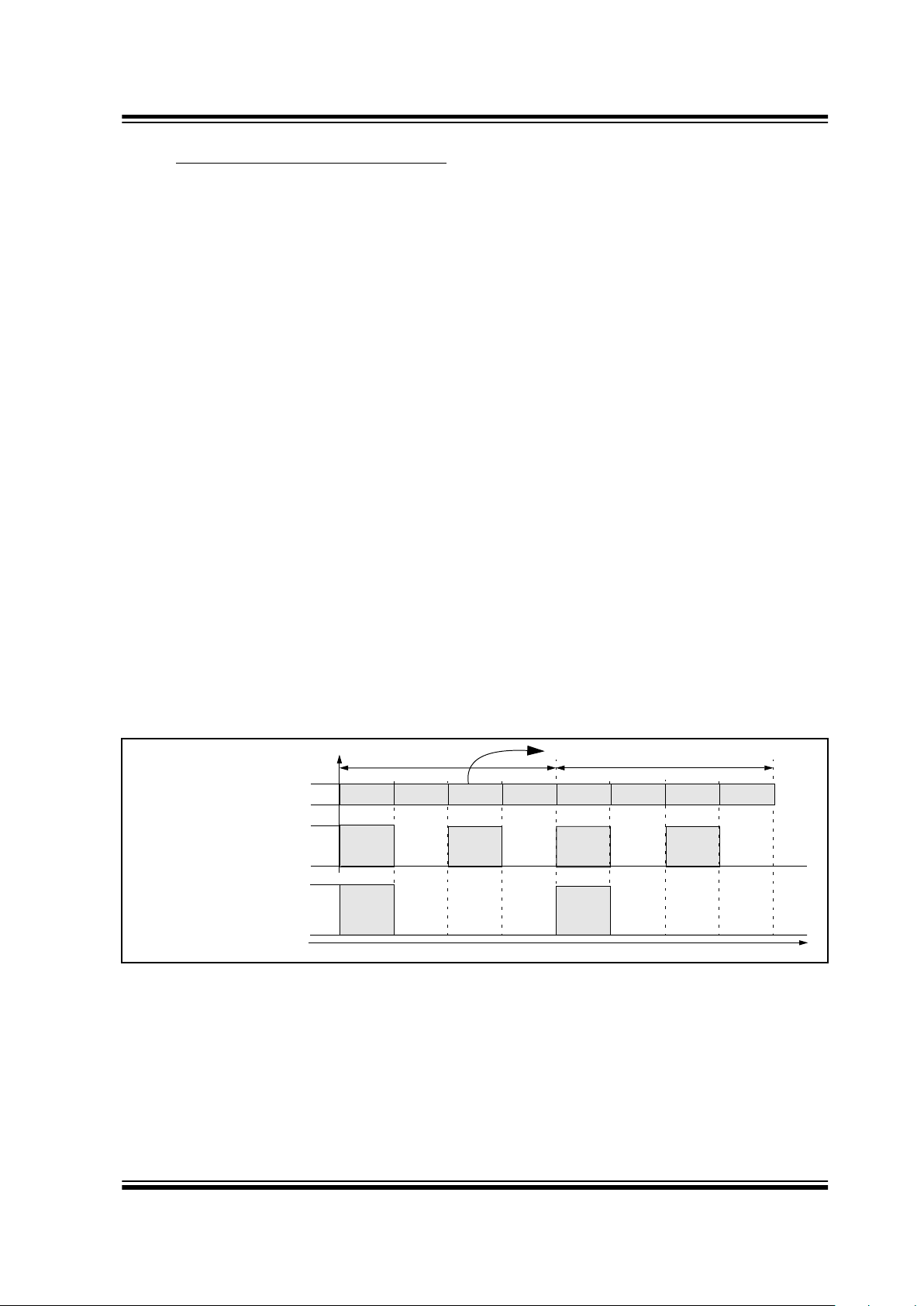
FIGURE 2-13: QUE COUNTER TIMING DIAGRAM
Note 1: The QUE will not overflow.
2: The button must be pressed f or more than
50 ms.
Input
Sx
DIO
Transmission
1st Button Press All Buttons Released 2nd Button Press
T
LOW>30 ms
t = 0
t > 50 ms
t <2S
t = 0
QUE = 00
2
QUE = 01
2
•Patents have been applied for.
Page 13

HCS410
1997 Microchip Technology Inc. Preliminary DS40158C-page 13
2.3.9 LED OUTPUT
The S2/LED line can be used to drive a LED when the
HCS410 is transmitting. If this option is enabled in the
configuration word the S2 line is driven high periodically when the HCS410 is transmitting as shown in
Figure 2-14. The LED output operates with a 30 ms on
and 480 ms off duty cycle when the supply voltage is
above the level indicated by the V
LOW bit in the config-
uration word. When the supply v oltage drops below the
voltage indicated by the VLOW bit the HCS410 will indicate this by turning the LED on for 200ms at the start of
a transmission and remain off for the rest of the transmission.
2.3.10 DELAYED INCREMENT
The HCS410 has a delayed increment feature that
increments the counter by 12, 20 seconds after the last
button press occurred. The 20-second time-out is reset
and the queue counter will increment if another press
occurs before the 20 seconds expires. The queue
counter is cleared after the buttons have been released
for more than 2 seconds. Systems that use this f eature
will circumvent the latest jamming-code grabbing
attackers.
2.3.11 OTHER CONFIGURABLE OPTIONS
Other configurable code hopping options include an
• Transmission-rate selection
• Extended serial number.
These are described in more detail in Section 3.7.
FIGURE 2-14: LED INDICATION DURING TRANSMISSION
200 ms 280 ms
400 ms
30 ms
S Input
LED
VDD = VLOW Level
LED
V
DD < VLOW LEVEL
Page 14

HCS410
DS40158C-page 14 Preliminary 1997 Microchip Technology Inc.
2.4 IFF Mode
IFF mode allows the decoder to perform an IFF validation, to write to the user EEPROM and to read from the
user EEPROM. Each operation consists of the decoder
sending an opcode data and the HCS410 giving a
response.
There are two IFF modes: IFF1 and IFF2. IFF1 allows
only one key IFF, while IFF2 allows two keys to be used.
It is possible to use the HCS410 as an IFF token without using a magnetic field for coupling. The HCS410
can be directly connected to the data line of the
decoder as shown in Figure 2-3. The HCS410 gets its
power from the data line as it would in normal transponder mode. The communication is identical to the communication used in transponder mode.
2.4.1 IFF MODE ACTIVATION
The HCS410 will enter IFF mode if the capacitor/induc-
tor resonant circuit generates a voltage greater than
approximately 1.0 volts on LC0. After the verified application of power and elapse of the normal reset period,
the device will start responding by pulsing the DAT A line
(LC0/1) with pulses as shown in Figure 2-17. This
action will continue until the pulse train is terminated by
receiving a start signal of duration 2T
E, on the LC
inputs before the next expected marker pulse. The
device now enters the IFF mode and expects to receiv e
an ‘Opcode’ and a 0/16/32-bit Data-stream to react on.
The data rate (T
E) is determined by the TBSL bits in the
configuration word. See Section 3.0 for additional
details.
2.4.2 IFF DECODER COMMANDS
As shown in Figure 2-15, a logic 1 and 0 are differenti-
ated by the time between two rising edges. A long pulse
indicates a 1; a short pulse, a 0.
FIGURE 2-15: MODULATION FOR IFF COMMUNICATION
FIGURE 2-16: OVERVIEW OF IFF OPERATION
Note: When IFF2 is enabled, seed transmissions
will not be allowed.
0
1
3 TE
1TE
5 TE
0
1
TE TE
2 TE TE
Start or
previous
bit
1 TE
PPM Decoder Commands PPM Encoder Response
Activate Opcode
32/16-bit Challenge 32/16-bit IFF Response
Opcode
Activate
Opcode 16 bit Data OK Opcode
Activate Opcode 16 bit Data
IFF
WRITE
READ
Opcode
Page 15

HCS410
1997 Microchip Technology Inc. Preliminary DS40158C-page 15
FIGURE 2-17: DECODER IFF COMMANDS AND WAVEFORMS
Ack pulses Opcode
Transport
Code
32 bits
Ack
Writing
bit0
bit1
bit2
bit3
bit4
TBITC
TE
Data
16 bits
TOTD TTTD
TWR
Only when writing Serial
Number, Config or IFF
programming
Serial number
1 to 32 bits
Encoder
Select
Ack
0
0
000
Ack pulses
Challenge
16/32 bits
Response
16/32 bits
Ack pulses Opcode TOTD
Response
Start TRT
16 bits
01
Ack pulsesRead
Write/Program
Challenge
Encoder Select
2 TE
Repeat 18 times for programming
TABLE 2-3: IFF TIMING PARAMETERS
Parameter Symbol Minimum Typical Maximum Units
Time Element
IFFB = 0
IFFB = 1
TE —
—
200
100
—
—
µs
PPM Command Bit Time
Data = 1
Data = 0
TBITC 3.5
5.5
4
6
—
—
TE
PPM Response Bit Time
Data = 1
Data = 0
T
BITR —
—
2
3
—
—
TE
PPM Command Minimum High Time TPMH 1.5 — — TE
Response Time (Minimum for Read) TRT 6.5 — — ms
Opcode to Data Input Time T
OTD 1.8 — — ms
Transport Code to Data Input Time T
TTD 6.8 — — ms
IFF EEPROM Write Time (16 bits) T
WR — — 30 ms
Page 16

HCS410
DS40158C-page 16 Preliminary 1997 Microchip Technology Inc.
2.4.3 HCS410 RESPONSES
The responses from the HCS410 are in PPM format.
See Figure 2-17 for additional information
2.4.4 IFF RESPONSE
The 16/32-bit response to a 16/32-bit challenge, is
transmitted once, after which the device is ready to
accept another command. The same applies to the
result of a Read command. The opcode written to the
device specifies the challenge length and algorithm
used.
2.4.5 IFF WRITE
The decoder can write to USER[0:3], SER[0:1], and the
configuration word in the EEPROM.
After the HCS410 has written the word into the
EEPROM, it will give two ackno wledge pulses (T
E wide
and T
E apart) on the LC pins.
When writing to the serial number or configuration
word, the user must send the transport code before the
write will begin (Section 3.4) .
2.4.6 IFF READ
The decoder can read USER[0:3], SER[0:1], and the
configuration word in the EEPROM. After the data has
been read, the device is ready to receive a command
again.
Each read command is followed by a 16-bit data
response. The response always starts with a leading
preamble of 01
2
and then the 16-bits of data.
2.4.7 IFF PROGRAMMING
Upon receiving a programming opcode and the trans-
port code, the EEPROM is erased (Section 3.4).
Thereafter, the first 16 bits of data can be written. After
indicating that a write command has been successfully
completed the device is ready to receive the next 16
bits. After a complete memory map was receiv ed, it will
be transmitted in PPM format on the LC pins as 16-bit
words. This enables wireless programming of the
device.
After the EEPROM is erased, the configuration word is
reloaded. This results in oscillator tuning bits of 0000
being used during programming. When using IFF programming, the user should read the configuration word
and store the oscillator bits in the memory map to be
programmed. A program command should be sent and
the next set of ACK pulses transmitted by the HCS410
should be used to determine the T
E. A second prog ram
command can then be sent, and the device programmed using the T
E just calibrated.
FIGURE 2-18: IFF INDUCTIVE IN RF OUT
Note: If the configuration word is written, the
device must be reset to allow the new configuration settings to come into effect.
Preamble
Header
Response
(32 bits)
Fixed Code
(37 bits)
PWM
LCI0/1
32-bit Response
16-bit
Response
16-bit
Response
Encoder
Select ACK
Opcode
(Read)
Response
(16 bits)
Next
Ack
Page 17

HCS410
1997 Microchip Technology Inc. Preliminary DS40158C-page 17
2.5 IFF Opcodes
TABLE 2-4: LIST OF IFF COMMANDS
Command Description Expected data In Response
00000 Select HCS410, used if Anticolli-
sion enabled
1 to 32 bits of the serial number
(SER)
Encoder select acknowledge if
SER match
00001 Read configuration word None 16-bit configuration word
00010 Read high serial number None Higher 16 bits of serial number
(SER1)
00011 Read low serial number None Lower 16 bits of serial number
(SER0)
00100 Read user area 0 None 16 Bits of User EEPROM USR0
00101 Read user area 1 None 16 Bits of User EEPROM USR1
00110 Read user area 2 None 16 Bits of User EEPROM USR2
00111 Read user area 3 None 16 Bits of User EEPROM USR3
01000 Program HCS410 EEPROM Transport code (32 bits); Com-
plete memory map: 18 x 16 bit
words (288 bits)
Write acknowledge pulse after
each 16-bit word, 288 bits trans-
mitted in 18 bursts of 16-bit
words
01001 Write configuration word Transport code (32 bits); 16 Bit
configuration word
Write acknowledge pulse
01010 Write high serial number Transport code (32 bits); Higher
16 bits of serial number (SER1)
Write acknowledge pulse
01011 Write low serial number Transport code (32 bits); Lower
16 bits of serial number (SER0)
Write acknowledge pulse
01100 Write user area 0 16 Bits of User EEPROM USR0 Write acknowledge pulse
01101 Write user area 1 16 Bits of User EEPROM USR1 Write acknowledge pulse
01110 Write user area 2 16 Bits of User EEPROM USR2 Write acknowledge pulse
01111 Write user area 3 16 Bits of User EEPROM USR3 Write acknowledge pulse
1X000 IFF1 using key-1 and IFF
algorithm
32-Bit Challenge 32 Bit Response
1X001 IFF1 using key-1 and HOP
algorithm
32-Bit Challenge 32 Bit Response
1X100 IFF2 32-bit using key-2 and IFF
algorithm
32-Bit Challenge 32 Bit Response
1X101 IFF2 32-bit using ke y-2 and HOP
algorithm
32-Bit Challenge 32 Bit Response
Page 18

HCS410
DS40158C-page 18 Preliminary 1997 Microchip Technology Inc.
2.6 IFF Special Features
2.6.1 ANTI-COLLISION (ACOLI)
When the ACOLI bit is set in the configuration word,
anti-collision mode is entered. The HCS410 will start
sending ACK pulses when it enters a magnetic field.
The ACK pulses stop as soon as the HCS410 detects
a start bit from the decoder. A ‘select encoder’ opcode
(00000) is then sent out by the decoder, followed by a
32-bit serial number. If the serial number matches the
HCS410’s serial number, the HCS410 will acknowledge with the acknowledge sequence as shown in
Figure 2-19. The HCS410 can then be addressed as
normal. If the serial number does not match, the IFF
encoder will stop transmitting ACK pulses until it is
either removed from the field or the correct serial number is given.
FIGURE 2-19: SERIAL NUMBER CORRECT
ACKNOWLEDGE SEQUENCE
2.6.2 TRANSPONDER IN/RF OUT
When in transponder mode with ACOLI and XPRF set,
the outputs of the HCS410’s LC0:LC1 pins are echoed
on the PWM output line. After transmitting the data on
the LC pins, the data is then transmitted on the PWM
line. The transmission format mirrors a code hopping
transmission. The response replaces the 32-bit code
hopping portion of the transmission. If the response is
a 16-bit response, the 16 bits are duplicated to make up
the 32-bit code hopping portion. The preamble, serial
number, CRC, and queuing bits are all transmitted as
normal (Figure 2-18).
This feature will be used in applications which use RF
for long distance unidirectional authentication and
short distance IFF.
2.6.3 INTELLIGENT DAMPING
If the LC circuit on the transponder has a high Q-factor ,
the circuit will keep on resonating for a long time after
the field has been shut down by the decoder. This
makes fast communication from the decoder to the
HCS410 difficult. If the IDAMP bit is set to 0, the
HCS410 will clamp the LC pins for 5 µs every 1/4 T
E,
whenever the HCS410 is expecting data from the
decoder. Refer to Figure 2-18 for timing details. This
option can be set in the configuration word.
2.7 LED Indicator
If a signal is detected on LC0, the LED pin goes high for
30 ms every 8s (IFFB = 0) or 4s (IFFB 1) to indicate that
the power source is charging.
FIGURE 2-20: LED INDICATOR WHEN CHARGING POWER SOURCE
LC0/1
TE
TE
3 TE
LC0
LED
IFFB = 0
LED
IFFB = 1
4s
8s
30 ms
2s 4s 30 ms
Page 19

HCS410
1997 Microchip Technology Inc. Preliminary DS40158C-page 19
3.0 EEPROM ORGANIZATION AND
CONFIGURATION
The HCS410 has nonvolatile EEPROM memory which
is used to store user programmable options. This information includes encoder keys, serial number , and up to
64-bits of user information.
The HCS410 has two modes in which it operates as
specified by the configuration word. In the first mode
the HCS410 has a single encoder key which is used for
encrypting the code hopping portion of a CH Mode
transmission and generating a response during IFF validation. Seed transmissions are allowed in this mode.
In the second mode the HCS410 is a transponder
device with two encoder keys.
The two different operating modes of the HCS410 lead
to different EEPROM memory maps.
In IFF1 mode, the HCS410 can act as a code hopping
encoder with Seed transmission, and as an IFF token
with one key.
In IFF2 mode, the HCS410 is able to act as a code hopping transmitter and an IFF token with two encoder
keys.
3.1 Encoder Key 1 and 2
The 64-bit encoder key1 is used by the transmitter to
create the encrypted message transmitted to the
receiver in Code Hopping Mode. An IFF operation, can
use encoder key1 or key2 to generate the response to
a challenge received. The key(s) is created and programmed at the time of production using a key generation algorithm. Inputs to the key generation algorithm
are the serial number or seed for the particular
transmitter being used and a secret manufacturer’s
code. While a number of key generation algorithms are
supplied by Microchip, a user may elect to create their
own method of key generation. This may be done providing that the decoder is programmed with the same
means of creating the key for decryption purposes. If a
seed is used (CH Mode), the seed will also form part of
the input to the key generation algorithm.
3.2 Discrimination Value and Overflow
The discrimination value forms part of the code hopping portion of a code hopping transmission. The least
significant 10 bits of the discrimination value are typically set to the least significant bits of the serial number.
The most significant 2 bits of the discrimination value
are the overflow bits (OVR1: O VR0). These are used to
extend the range of the synchronization counter . When
the synchronization counter wraps from FFFF
16
to
0000
16
OVR0 is cleared and the second time a wrap
occurs OVR1 is cleared.
Once cleared, the overflow bits cannot be set again,
thereby creating a permanent record of the counter
overflow.
3.3 16-bit Synchronization Counter
This is the 16-bit synchronization counter value that is
used to create the code hopping portion for transmission. This value will be changed after every transmission. The synchronization counter is not used in IFF
mode.
IFF1 Mode
64-bit Encoder Key 1
64-bit Seed/Transport Code
(SEED0, SEED1, SEED2, SEED3)
32-bit Serial Number
(SER0, SER1)
64-bit User Area
(USR0, USR1, USER2, USR3)
10-bit Discrimination Value and 2 Overflow Bits.
16-bit Synchronization Counter
Configuration Data
IFF2 Mode
64-bit Encoder Key 1
64-bit Encoder Key 2/Transport Code
32-bit Serial Number
(SER0, SER1)
64-bit User EEPROM
(USR0, USR1, USER2, USR3)
10-bit Discrimination Value and 2 Overflow Bits.
16-bit Synchronization Counter
Configuration Data
*Patents have been applied for.
Page 20

HCS410
DS40158C-page 20 Preliminary 1997 Microchip Technology Inc.
3.4 60/64-bit Seed Word/Transport Code
This is the 60-bit seed code that is transmitted when
seed transmission is selected. This allows the system
designer to implement the secure learn feature or use
this fixed code word as part of a different key generation/tracking process or purely as a fixed code transmission. The seed is not available in IFF2-mode. A
Seed transmission can be initiated in two ways,
depending on the button inputs (Figure 3-1)
Seed transmission is available for function codes
(Table 2-2) S[2:0] = 111 and S[2:0] = 011 (delayed).
The delayed seed transmission starts with a normal
code hopping transmission being transmitted for 3 seconds, before switching to a seed tr ansmission. The two
seed transmissions are shown in Figure 3-1.
The least significant 32-bits of the seed are used as the
transport code. The transport code is used to write-protect the serial number, configuration word, as well as
preventing accidental programming of the HCS410
when in IFF mode.
3.5 Encoder Serial Number
There are 32 bits allocated for the serial number and a
selectable configuration bit (XSER) determines
whether 32 or 28 bits will be transmitted. The serial
number is meant to be unique for every transmitter.
3.6 User Data
The 64-bit user EEPROM can be reprogrammed and
read at any time using the IFF interface.
FIGURE 3-1: SEED TRANSMISSION
Note: If both SEED and TMPSD are set, IFF2
mode is enabled.
All examples shown with XSER = 1 & SEED = 1
When S[2:0] = 111, the 3-second delay is not applicable:
Que [1:0], CRC [1:0], SEED_3 (12 bits) SEED_2 SEED_1 SEED_0
Data transmission direction
For S[2:0] = 011 before the 3-second delay:
16-bit Data Word 16-bit Counter
Encrypt
SER_1 SER_0 Encrypted Data
For S[2:0] = 011 after the 3-second delay (Note 1):
Data transmission direction
Note 1: For Seed Transmission, SEED_3 and SEED_2 are transmitted instead of SER_1 and SER_0, respectively.
SEED_3 (12 bits) SEED_2 SEED_1 SEED_0
Data transmission direction
VLOW, S[2:0]
Que [1:0], CRC [1:0]
+ VLOW, S [2:0]
Que [1:0], CRC [1:0],
VLOW, S [2:0]
*Patents have been applied for.
Page 21

HCS410
1997 Microchip Technology Inc. Preliminary DS40158C-page 21
3.7 Configuration Data
The configuration data is used to select various
encoder options. Further explanations of each of the
bits are described in the following sections.
3.7.1 CWBE: CODE WORD BLANKING ENABLE
BSL: BAUD RATE SELECT
Selecting this option allows code blanking as shown in
Table 3-3. If this option is not selected, all code words
are transmitted.
3.7.2 IDAMP: INTELLIGENT DAMPING
If IDAMP is set to ‘1’ intelligent damping is disabled.
3.7.3 SEED, TMPSD: SEED TRANSMISSION
3.7.4 OSC: OSCILLATOR TUNING BITS
These bits allow the onboard oscillator to be tuned to
within 10% of the nominal oscillator speed over both
temperature and voltage.
TABLE 3-1: CONFIGURATION OPTIONS
SEED
Symbol Description
CWBE Code Word Blanking Enable
IDAMP Intelligent Damping for High Q LC Tank.
SEED/
IFF2
Enable Seed Transmissions
TMPSD/
IFF2
Temporary Seed Transmissions
OSC0:3 Onboard Oscillator Tuning Bits
MTX3 Minimum 3 Code Words Transmitted
VLOW Low Voltage Trip Point Selection
LED Enable LED output
BSL0:1 Baudrate Select
TBSL Transponder Baud Page
MANCH Manchester Modulation Mode
ACOLI Anti Collision Communication Enable
XPRF Passive Proximity Activation
DINC Delayed Increment Enable
XSER Extended Serial Number
SEED TMPSD Description
0 0 No Seed
0 1 Seed Limited
1 0 Always Enabled
1 1 IFF2/No Seed
TABLE 3-2: OSCILLATOR TUNING
OSC Description
1000 Fastest
1001
1010
•
•
•
1111
Faster
0000 Nominal
0001
0010
•
•
•
0110
Slower
0111 Slowest
TABLE 3-3: BAUD RATE SELECTION
Code Hopping Transmissions (TE) Transponder Communication (TE)
BSL 1 BSL 0 PWM Manchester
Codes Wor d
T ransmitted*
TBSL PPM
0 0 400 µs 800 µs All 0 200 µs
0 1 200 µs 400 µs 1 of 2 — —
1 0 100 µs 200 µs 1 of 2 — —
1 1 100 µs 200 µs 1 of 4 1 100 µs
*If code word blanking is enabled.
Page 22

HCS410
DS40158C-page 22 Preliminary 1997 Microchip Technology Inc.
3.7.5 MTX3: MINIMUM CODE WORDS
COMPLETED
If this bit is set, the HCS410 will transmit a minimum of
3 words before it powers itself down. If this bit is
cleared, the HCS410 will only complete the current
transmission. This feature will only work if V
DD is con-
nected directly to the battery as shown in Figure 2-1.
3.7.6 V
LOW: LOW V OLTAGE TRIP POINT
The low voltage trip point select bit is used to tell the
HCS410 what Vdd le v el is being used. This inf ormation
will be used by the device to determine when to send
the voltage low signal to the receiver. When this bit is
set, the Vdd level is assumed to be operating from a 5
volt or 6 volt supply. If the bit is cleared, then the Vdd
level is assumed to be 3.0 v olts. Refer to Figure 5-3 f or
voltage trip point. When the battery reaches the Vlow
point, the LED will flash once for 200 ms on during a
code hopping transmission.
3.7.7 LED: OUTPUT ENABLE
If this bit is set, the S2 doubles as an LED output line.
If this bit is cleared (0), S2 is only used as an input.
3.7.8 TBSL: TRANSPONDER BAUD RATE
SELECT
This option selects the baud rate for IFF communication between a T
E of 100 µs or 200 µs.
3.7.9 MANCH: MANCHESTER CODE
ENCODING
MANCH selects between Manchester code modulation
and PWM modulation in code hopping mode. If
MANCH = 1, Manchester code modulation is selected.
If MANCH is cleared, PWM modulation is selected.
3.7.10 ACOLI: ANTI-COLLISION
COMMUNICATION AND
XPRF: TRANSPONDER ECHOING
ON PWM OUTPUT
ACOLI = 1, XPRF = 0
If ACOLI is set the anti-collision operation during bidirectional transponder mode (IFF) is enabled. This
feature is useful in situations where multiple transponders enter the magnetic field simultaneously.
ACOLI = 0, XPRF = 1
If XPRF is set, and ACOLI is cleared, proximity activation is enabled. the HCS410 star ts sending out ACK
pulses when it detects a magnetic field. If the HCS410
doesn’t receive a start bit from the decoder within 50
ms of sending the first set of ACK pulses, the HCS410
will transmit a code hopping transmission on LC and
PWM pins for 2 seconds.
ACOLI = 1, XPRF = 1
If both the ACOLI and XPRF are set, all of the HCS410
transponder responses are echoed on the PWM output, as described in Section 2.6.2.
3.7.11 DINC: DELAYED INCREMENT
If DINC is set to ‘1’, the delayed increment feature is
enabled. If DINC is cleared, the counter only increments once each time the button is pressed.
3.7.12 XSER: EXTENDED SERIAL NUMBER
If XSER is set, the full 64-bit SEED number is
transmitted. If XSER is cleared, the four most significant bits of the serial number are substituted by
S[2:0] = S2:S1:S0: 0 and is compatible with the
HCS200/300/301.
Page 23
HCS410
1997 Microchip Technology Inc. Preliminary DS40158C-page 23
4.0 INTEGRATING THE HCS410
INTO A SYSTEM
Use of the HCS410 in a system requires a compatible
decoder. This decoder is typically a microcontroller with
compatible firmware. Firmware routines that accept
transmissions from the HCS410, decrypt the code hopping portion of the data stream and perform IFF functions are available. These routines provide system
designers the means to develop their own decoding
system.
4.1 Key Generation
The serial number for each transmitter is programmed
by the manufacturer at the time of production. The
generation of the encoder key is done using a ke y generation algorithm (Figure 4-1). Typically, inputs to the
key generation algorithm are the serial number of the
transmitter or seed value, and a 64-bit manufacturer’s
code. The manuf acturer’ s code is chosen by the system
manufacturer and must be carefully controlled. The
manufacturer’s code is a pivotal part of the overall
system security.
FIGURE 4-1: CREATION AND STORAGE OF ENCODER KEY DURING PRODUCTION
Transmitter
Manufacturer’s
Serial Number or
Code
Encoder
Key
Key
Generation
Algorithm
Serial Number
Encoder Key
Sync Counter
.
.
.
HCS410 EEPROM Array
Seed
Page 24

HCS410
DS40158C-page 24 Preliminary 1997 Microchip Technology Inc.
4.2 Learning an HCS410 to a Receiver
In order for a transmitter to be used with a decoder , the
transmitter must first be ‘learned’. Several learning
strategies can be followed in the decoder implementation. When a transmitter is learned to a decoder, it is
suggested that the decoder stores the serial number
and current synchronization counter value (synchronization counter stored in CH Mode only) in EEPROM.
The decoder must keep track of these values for every
transmitter that is learned (Figure 4-2 and Figure 4-3).
FIGURE 4-2: TYPICAL CH MODE LEARN
SEQUENCE
The maximum number of transmitters that can be
learned is only a function of how much EEPROM
memory storage is available. The decoder must also
store the manufacturer’s code in order to learn an
HCS410, although this value will not change in a typical
system so it is usually stored as part of the microcontroller ROM code. Storing the manufacturer’s code as
part of the ROM code is also better for security reasons.
FIGURE 4-3: TYPICAL IFF LEARN
SEQUENCE
Enter Learn
Mode
Wait for Reception
of a Valid Code
Generate Key
from Serial Number
Use Generated Key
to Decrypt
Compare Discrimination
Value with Fixed Value
Equal
Wait for Reception
of Second Valid Code
Compare Discrimination
Value with Fixed Value
Use Generated Key
to Decrypt
Equal
Counters
Encoder key
Serial number
Synchronization counter
Sequential
?
?
?
Exit
Learn successful Store:
Learn
Unsuccessful
No
No
No
Yes
Yes
Yes
Enter Learn
Wait for token
to be detected
Read
Generate Key
From Serial
Perform IFF
with T ok en
Compare T ok en
and expected
response
Token and
Response
Equal?
Exit
Serial Number
No
Yes
Learn successful
Serial number
Encoder key
Number
Store:
Mode
Page 25

HCS410
1997 Microchip Technology Inc. Preliminary DS40158C-page 25
4.3 CH Mode Decoder Operation
In a typical decoder operation (Figure 4-4), the key
generation on the decoder side is done by taking the
serial number from a transmission and combining that
with the manufacturer’s code to create the same
encoder key that is stored in the HCS410. Once the
encoder key is obtained, the rest of the transmission
can be decrypted. The decoder waits for a tr ansmission
and immediately checks the serial number to
determine if it is a learned transmitter. If it is, the code
hopping portion of the transmission is decrypted using
the stored key. It uses the discrimination bits to determine if the decryption was valid. If everything up to this
point is valid, the synchronization counter value
is evaluated.
FIGURE 4-4: TYPICAL CH MODE
DECODER OPERATION
?
Transmission
Received
Does
Serial Number
Match
?
Decrypt T ransmission
Is
Decryption
Valid
?
Is
Counter
Within 16
?
Is
Counter
Within 32K
?
Update
Counter
Execute
Command
Save Counter
in T emp Location
Start
No
No
No
No
Yes
Yes
Yes
Yes
Yes
and
No
No
Page 26
HCS410
DS40158C-page 26 Preliminary 1997 Microchip Technology Inc.
4.3.1 SYNCHRONIZATION WITH DECODER
The K
EELOQ
technology features a sophisticated
synchronization technique (Figure 4-5) which does not
require the calculation and storage of future codes. If
the stored counter value for that particular transmitter
and the counter value that was just decrypted are
within a window of say 16, the counter is stored and the
command is executed. If the counter value was not
within the single operation window, but is within the
double operation window of say 32K window , the tr ansmitted synchronization counter value is stored in temporary location and it goes back to waiting for another
transmission. When the next valid transmission is
received, it will compare the new value with the one in
temporary storage. If the two v alues are sequential, it is
assumed that the counter had just gotten out of the single operation ‘window’, but is now back in sync, so the
new synchronization counter value is stored and the
command executed. If a transmitter has somehow gotten out of the double operation window, the transmitter
will not work and must be relearned. Since the entire
window rotates after each valid transmission, codes
that have been used are part of the ‘blocked’ (32K)
codes and are no longer valid. This eliminates the possibility of grabbing a previous code and retransmitting
to gain entry.
FIGURE 4-5: SYNCHRONIZATION WINDOW
FIGURE 4-6: BASIC OPERATION OF A CODE HOPPING RECEIVER (DECODER)
Note: The synchronization method described in
this section is only a typical
implementation and because it is usually
implemented in firmware, it can be altered
to fit the needs of a particular system
Blocked
Entire Window
rotates to eliminate
use of previously
used codes
Current
Position
(32K Codes)
Double
Operation
(32K Codes)
Single Operation
Window (16 Codes)
Button Press
Information
EEPROM Array
Encoder Key
32 Bits of
Encrypted Data
Serial Number
Received Information
Decrypted
Synchronization
Counter
Check for
Match
Check for
Match
KEELOQ
Algorithm
Decryption
Sync Counter
Serial Number
Manufacturer Code
Page 27

HCS410
1997 Microchip Technology Inc. Preliminary DS40158C-page 27
4.4 IFF Decoder Operation
In a typical IFF decoder, the key generation on the
decoder side is done by reading the serial number from
a token and combining that with the manufacturer’s
code to recreate the encoder key that is stored on the
token. The decoder polls for the presence of a token.
Once detected the decoder reads the serial number. If
the token has been learned, the decoder sends a challenge and reads the token’s response. The decoder
uses the encoder key stored in EEPROM and decrypt
response. The decrypt response is compared to the
challenge. If they match the appropriate output is activated.
FIGURE 4-7: TYPICAL IFF DECODER
OPERATION
FIGURE 4-8: BASIC OPERATION OF AN IFF RECEIVER (DECODER)
Start
Token
Detected?
Read Serial
Does
Serial Number
Match?
Send Challenge
and Read
Decrypt the
Response
Does
Challenge &
Match?
Execute Command
No
No
No
Yes
Yes
Yes
Response
Number
Decrypt response
IFF Key
Serial Number
KEELOQ
IFF
Algorithm
Decrypted
EEPROM Array
Manufacturer
Code
Serial Number Response
Check for
Match
Response
Written to HCS410
Challenge
Information read from HCS410
Page 28

HCS410
DS40158C-page 28 Preliminary 1997 Microchip Technology Inc.
5.0 ELECTRICAL CHARACTERISTICS
TABLE 5-1: ABSOLUTE MAXIMUM RATING
Symbol Item Rating Units
V
DD Supply voltage -0.3 to 6.6 V
V
IN* Input voltage -0.3 to VDD + 0.3 V
V
OUT Output voltage -0.3 to VDD + 0.3 V
I
OUT Max output current 50 mA
T
STG Storage temperature -55 to +125 C (Note)
T
LSOL Lead soldering temp 300 C (Note)
V
ESD ESD rating (Human Body Model) 4000 V
Note: Stresses above those listed under “ABSOLUTE MAXIMUM RATINGS” may cause permanent damage to
the device.
* If a battery is inserted in reverse, the protection circuitry switches on, protecting the device and draining the
battery.
TABLE 5-2: DC AND TRANSPONDER CHARACTERISTICS
Commercial (C): Tamb = 0°C to 70°C
Industrial (I): Tamb = -40°C to 85°C
2.0V < V
DD < 6.3V
Parameter Symbol Min Typ
1
Max Unit Conditions
Average operating current
2
IDD (avg) —
50
160
100
300
µA
V
DD = 3.0V
V
DD = 6.3V
Programming current
I
DDP
— 1.0
2.2
1.8
3.5
mA
VDD = 3.0V
V
DD = 6.3V
Standby current I
DDS — 0.1 100 nA
High level input voltage V
IH 0.55 VDD —VDD + 0.3 V
Low level input voltage V
IL -0.3 — 0.15 VDD V
High level output voltage V
OH
0.8 VDD
0.8 VDD
——
V
VDD = 2V, IOH =- .45 mA
V
DD = 6.3V, IOH,= -2 mA
Low level output voltage V
OL
—
—
—
—
0.08 VDD
0.08 VDD
V
V
DD = 2V, IOH = 0.5 mA
V
DD = 6.3V,IOH = 5mA
LED output current I
LED 3.0 4.0 7.0 mA VDD = 3.0V, VLED = 1.5V
Switch input resistor RS 40 60 80 kΩ
PWM input resistor R
PWM 80 120 160 kΩ
LC input current I
LC — — 10.0 mA VLCC=15 VP-P
LC input clamp voltage VLCC —15— VILC <10 mA
LC induced output current V
DDI — 5.0 mA VLCC > 10V
LC induced output voltage
V
DDV
5.0
4.5
6.3
5.6
6.8
6.8
V
10 V < VLCC, IDD = 0 mA
10 V < V
LCC, IDD = -1 mA
Carrier frequency
f
c — 125 — kHz
External LC Inductor value L — 900 — µH
External LC Capacitor value C — 1.8 — pF
Note 1: Typical values at 25°C.
2: No load connected.
3: LC inputs are clamped at 15 volts.
Page 29
HCS410
1997 Microchip Technology Inc. Preliminary DS40158C-page 29
FIGURE 5-1: POWER UP AND TRANSMIT TIMING
TABLE 5-3: POWER UP AND TRANSMIT TIMING REQUIREMENTS
VDD = +2.0 to 6.3V
Commercial (C):Tamb = 0°C to +70°C
Industrial (I): Tamb = -40°C to +85°C
Parameter Symbol Min Typ. Max Unit Remarks
Time to second button press T
BP 34 + Code
Word Time
38 + Code
Word Time
42 + Code
Word Time
ms (Note 1)
Transmit delay from button detect T
TD 34.2 38 41.8 ms (Note 2)
Debounce delay T
DB 27 30 33 ms
Auto-shutoff time-out period T
TO 18 20 22 s (Note 3)
Time to first LED on T
LST — 240 — ms
LED high-time T
LH —25—ms
LED high-time when battery low T
LHV — 200 — ms
LED low-time T
LL — 480 — ms
Note 1: T
BP is the time in which a second button can be pressed without completion of the first code word and the
intention was to press the combination of buttons.
2: Transmit delay maximum value if the previous transmission was successfully transmitted.
3: The auto-shutoff timeout period is not tested.
Button Press
Sn
Detect
T
DB
PWM
TTD
Code Word Transmission
TTO
Code
Word
1
Code
Word
2
Code
Word
3
Code
Word
n
T
BP
Page 30
HCS410
DS40158C-page 30 Preliminary 1997 Microchip Technology Inc.
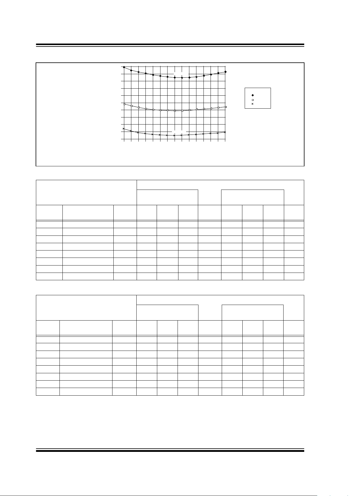
FIGURE 5-2: HCS410 NORMALIZED TE VS. TEMP
TABLE 5-4: CODE WORD TRANSMISSION TIMING PARAMETERS—PWM MODE
VDD = +2.0V to 6.3V
Commercial (C):Tamb = 0°C to +70°C
Industrial (I): Tamb = -40°C to +85°C
Code Words T ransmitted
BSL1 = 0,
BSL0 = 0
BSL1 = 0,
BSL0 = 1
Symbol Characteristic
Number
of TE
Min. Typ. Max.
Number
of TE
Min. Typ. Max. Units
TE Basic pulse element 1 360 400 440 1 180.0 200.0 220.0 µs
TBP PWM bit pulse width 3 1080 1200 1320 3 540.0 600.0 660.0 µs
TP Preamble duration 32 12 12.8 14 32 5.76 6.0 7.04 ms
TH Header duration 10 3.6 4.0 4.4 10 1.80 2.0 2.20 ms
THOP Code hopping duration 96 35 38.4 42 96 17.28 19.20 21.12 ms
TFIX Fixed code duration 111 39.96 44.4 48.84 111 19.98 22.20 24.42 ms
TG Guard time 46 16.6 18.4 20.2 46 8.3 9.6 10.1 ms
— Total transmit time 295 106.2 118.0 129.8 295 53.1 59.0 64.9 ms
Note: The timing parameters are not tested but derived from the oscillator clock.
VDD = +2.0V to 6.3V
Commercial (C): Tamb = 0°C to +70°C
Industrial (I): Tamb = -40°C to +85°C
Code Words T ransmitted
BSL1 = 1,
BSL0 = 0
BSL1 = 0,
BSL0 = 1
Symbol Characteristic
Number
of TE
Min. Typ. Max.
Number
of TE
Min. Typ. Max. Units
TE Basic pulse element 1 180.0 200.0 220.0 1 90.0 100.0 110.0 µs
TBP PWM bit pulse width 3 540.0 600.0 660.0 3 270.0 300.0 330.0 µs
TP Preamble duration 32 5.76 6.0 7.04 32 2.88 3.0 3.52 ms
TH Header duration 10 1.80 2.0 2.20 10 0.90 1.0 1.10 ms
THOP Code hopping duration 96 17.28 19.20 21.12 96 8.64 9.60 10.56 ms
T
FIX Fixed code duration 111 19.98 22.2 24.42 111 9.99 11.1 12.21 ms
TG Guard time 46 8.3 9.6 10.1 46 41 4.6 5.1 ms
— Total transmit time 295 53.1 59.0 64.9 295 26.6 29.5 32.5 ms
Note: The timing parameters are not tested but derived from the oscillator clock.
0.94
1.10
1.08
1.06
1.04
1.02
1.00
0.98
0.96
0.92
0.90
TE Min.
TE Max.
VDD LEGEND
= 2.0V
= 3.0V
= 6.0V
Typical
TE
Temperature °C
-50 -40 -30 -20 -10 0 10 20 30 40 50 60 70 80 90
Note: Values are for calibrated oscillator.
Page 31
HCS410
1997 Microchip Technology Inc. Preliminary DS40158C-page 31
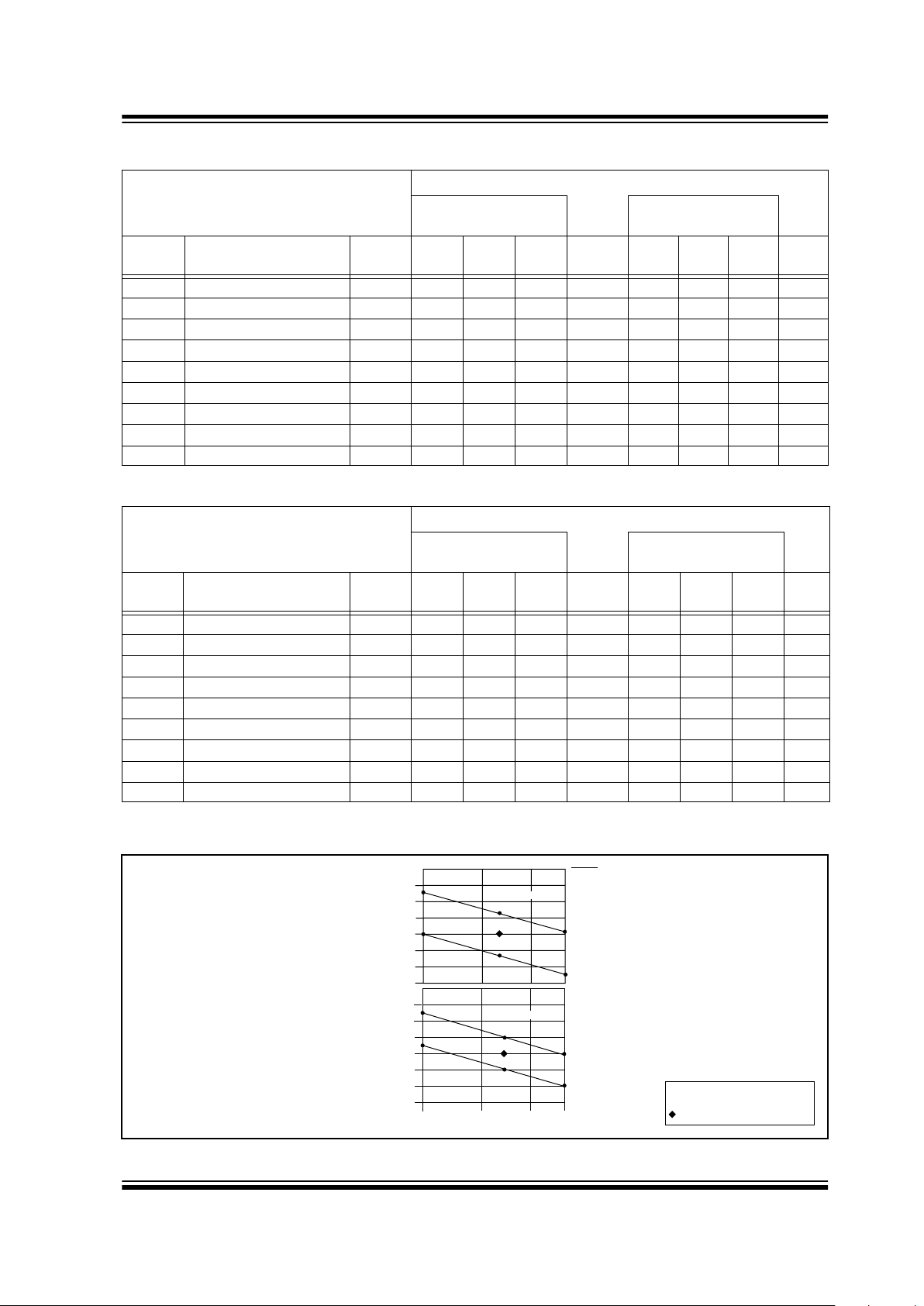
FIGURE 5-3: TYPICAL VOLTAGE TRIP POINTS
TABLE 5-5: CODE WORD TRANSMISSION TIMING PARAMETERS—MANCHESTER MODE
VDD = +2.0V to 6.3V
Commercial (C): Tamb = 0°C to +70°C
Industrial (I): Tamb = -40°C to +85°C
Code Words T ransmitted
BSL1 = 0,
BSL0 = 0
BSL1 = 0,
BSL0 = 1
Symbol Characteristic
Number
of TE
Min. Typ. Max.
Number
of TE
Min. Typ. Max. Units
TE
Basic pulse element 1 720.0 800.0 880.0 1.0 360.0 400.0 440.0 µs
TP
Preamble duration 32 23.04 25.60 28.16 32.0 11.52 12.80 14.08 ms
TH
Header duration 4 2.88 3.20 3.52 4.0 1.44 1.60 1.76 ms
TSTART
Start bit 2 1.44 1.60 1.76 2.0 0.72 0.80 0.88 ms
THOP
Code hopping duration 64 46.08 51.20 56.32 64.0 23.04 25.60 28.16 ms
TFIX
Fixed code duration 74 53.28 59.20 65.12 74 26.64 29.60 32.56 ms
TSTOP
Stop bit 2 1.44 1.60 1.76 2.0 0.72 0.80 0.88 ms
TG
Guard time 32 23.0 25.6 28.2 32 11.5 12.8 14.1 ms
— Total transmit time 210 151.2 168 184.8 210 75.6 84.0 92.4 ms
Note: The timing parameters are not tested but derived from the oscillator clock.
VDD = +2.0V to 6.3V
Commercial (C): Tamb = 0°C to +70°C
Industrial (I): Tamb = -40°C to +85°C
Code Words T ransmitted
BSL1 = 1,
BSL0 = 0
BSL1 = 1,
BSL0 = 1
Symbol Characteristic
Number
of TE
Min. Typ. Max.
Number
of TE
Min. Typ. Max. Units
TE
Basic pulse element 1 360.0 400.0 440.0 1.0 180.0 200.0 220.0 µs
TP
Preamble duration 32 11.52 12.80 14.08 32.0 5.76 6.40 7.04 ms
TH
Header duration 4 1.44 1.60 1.76 4.0 0.72 0.80 0.88 ms
TSTART
Start bit 2 0.72 0.80 0.88 2.0 0.36 0.40 0.44 ms
THOP
Code hopping duration 64 23.04 25.60 28.16 64.0 11.52 12.80 14.08 ms
TFIX
Fixed code duration 74 26.64 29.60 32.56 74 13.32 14.8 16.28 ms
TSTOP
Stop bit 2.0 0.72 0.80 0.88 2.0 0.36 0.40 0.44 ms
TG
Guard time 32 11.5 12.8 14.1 32 5.8 6.4 7.0 ms
— Total transmit time 210 75.6 84.0 92.4 210 37.8 42.0 46.2 ms
Note: The timing parameters are not tested but derived from the oscillator clock.
VLOW
Volts (V)
-40
05085
2.0
1.6
1.8
2.2
2.4
2.6
Temp (C)
VLOW sel = 0
4.4
4.0
4.2
3.8
4.6
4.8
5.0
VLOW sel = 1
2.8
Nominal VLOW trip point
Legend
Page 32

HCS410
DS40158C-page 32 Preliminary 1997 Microchip Technology Inc.
NOTES:
Page 33

HCS410
1997 Microchip Technology Inc. Preliminary DS40158C-page 33
NOTES:
Page 34

HCS410
DS40158C-page 34 Preliminary 1997 Microchip Technology Inc.
NOTES:
Page 35

HCS410
1997 Microchip Technology Inc. Preliminary DS40158C-page 35
HCS410 PRODUCT IDENTIFICATION SYSTEM
To order or obtain information, e.g., on pricing or delivery, refer to the factory or the listed sales office.
Sales and Support
Package:
P = Plastic DIP (300 mil Body), 8-lead
SN = Plastic SOIC (150 mil Body), 8-lead
ST = TSSOP (4.4 mm Body), 8-lead
Temperature
Range:
Blank = 0˚C to +70˚C
I = –40˚C to +85˚C
Device:
HCS410 Code Hopping Encoder
HCS410T Code Hopping Encoder (Tape and Reel)
HCS410 — /P
Data Sheets
Products supported by a preliminary Data Sheet may have an errata sheet describing minor operational differences and recommended workarounds. To determine if an errata sheet exists for a particular device, please contact one of the following:
1. Your local Microchip sales office.
2. The Microchip Corporate Literature Center U.S. FAX: (602) 786-7277.
3. The Microchip’s Bulletin Board, via your local CompuServe number (CompuServe membership NOT required).
Page 36

Information contained in this publication regarding device applications and the like is intended for suggestion only and ma y be superseded by updates. No representation or w arranty
is given and no liability is assumed by Microchip Technology Incor porated with respect to the accuracy or use of such information, or infringement of patents or other intellectual
property rights arising from such use or otherwise. Use of Microchip’s products as critical components in life support systems is not authorized except with express written approv al
by Microchip. No licenses are conveyed, implicitly or otherwise, under any intellectual property rights. The Microchip logo and name are registered trademarks of Microchip Technology Inc. in the U.S.A. and other countries. All rights reserved. All other trademarks mentioned herein are the property of their respective companies.
DS40158C-page 36
Preliminary
1997 Microchip Technology Inc.
All rights reserved. © 1/21/98, Microchip Technology Incorporated, USA. Wednesday, January 21, 1998 Printed on recycled paper.
M
AMERICAS
Corporate Office
Microchip T echnology Inc.
2355 West Chandler Blvd.
Chandler, AZ 85224-6199
Tel: 602-786-7200 Fax: 602-786-7277
Technical Support:
602 786-7627
Web:
http://www.microchip.com
Atlanta
Microchip T echnology Inc.
500 Sugar Mill Road, Suite 200B
Atlanta, GA 30350
Tel: 770-640-0034 Fax: 770-640-0307
Boston
Microchip T echnology Inc.
5 Mount Royal Avenue
Marlborough, MA 01752
Tel: 508-480-9990 Fax: 508-480-8575
Chicago
Microchip T echnology Inc.
333 Pierce Road, Suite 180
Itasca, IL 60143
Tel: 630-285-0071 Fax: 630-285-0075
Dallas
Microchip T echnology Inc.
14651 Dallas Parkway, Suite 816
Dallas, TX 75240-8809
Tel: 972-991-7177 Fax: 972-991-8588
Dayton
Microchip T echnology Inc.
Two Prestige Place, Suite 150
Miamisburg, OH 45342
Tel: 937-291-1654 Fax: 937-291-9175
Los Angeles
Microchip T echnology Inc.
18201 Von Karman, Suite 1090
Irvine, CA 92612
Tel: 714-263-1888 Fax: 714-263-1338
New Y ork
Microchip T echnology Inc.
150 Motor Parkway, Suite 202
Hauppauge, NY 11788
Tel: 516-273-5305 Fax: 516-273-5335
San Jose
Microchip T echnology Inc.
2107 North First Street, Suite 590
San Jose, CA 95131
Tel: 408-436-7950 Fax: 408-436-7955
Toronto
Microchip T echnology Inc.
5925 Airport Road, Suite 200
Mississauga, Ontario L4V 1W1, Canada
Tel: 905-405-6279 Fax: 905-405-6253
ASIA/PACIFIC
Hong Kong
Microchip Asia Pacific
RM 3801B, To wer Two
Metroplaza
223 Hing Fong Road
Kwai Fong, N.T., Hong Kong
Tel: 852-2-401-1200 Fax: 852-2-401-3431
India
Microchip T echnology Inc.
India Liaison Office
No. 6, Legacy, Convent Road
Bangalore 560 025, India
Tel: 91-80-229-0061 Fax: 91-80-229-0062
Japan
Microchip Technology Intl. Inc.
Benex S-1 6F
3-18-20, Shinyokohama
Kohoku-Ku, Yokohama-shi
Kanagawa 222 Japan
Tel: 81-45-471- 6166 Fax: 81-45-471-6122
Korea
Microchip T echnology Korea
168-1, Youngbo Bldg. 3 Floor
Samsung-Dong, Kangnam-Ku
Seoul, Korea
Tel: 82-2-554-7200 Fax: 82-2-558-5934
Shanghai
Microchip T echnology
RM 406 Shanghai Golden Bridge Bldg.
2077 Yan’an Road West, Hong Qiao District
Shanghai, PRC 200335
Tel: 86-21-6275-5700
Fax: 86 21-6275-5060
Singapore
Microchip T echnology Taiwan
Singapore Branch
200 Middle Road
#07-02 Prime Centre
Singapore 188980
Tel: 65-334-8870 Fax: 65-334-8850
ASIA/PACIFIC
(CONTINUED)
Taiwan, R.O.C
Microchip T echnology Taiwan
10F-1C 207
Tung Hua North Road
T aipei, Taiwan, ROC
Tel: 886-2-2717-7175 Fax: 886-2-2545-0139
EUROPE
United Kingdom
Arizona Microchip Technology Ltd.
505 Eskdale Road
Winnersh T riangle
Wokingham
Berkshire, England RG41 5TU
Tel: 44-1189-21-5858 Fax: 44-1189-21-5835
France
Arizona Microchip Technology SARL
Zone Industrielle de la Bonde
2 Rue du Buisson aux Fraises
91300 Massy, France
Tel: 33-1-69-53-63-20 Fax: 33-1-69-30-90-79
Germany
Arizona Microchip Technology GmbH
Gustav-Heinemann-Ring 125
D-81739 Müchen, Germany
Tel: 49-89-627-144 0 Fax: 49-89-627-144-44
Italy
Arizona Microchip Technology SRL
Centro Direzionale Colleoni
Palazzo Taurus 1 V. Le Colleoni 1
20041 Agrate Brianza
Milan, Italy
Tel: 39-39-6899939 Fax: 39-39-6899883
1/13/98
W
ORLDWIDE
S
ALES
AND
S
ERVICE
 Loading...