

Microchip Technology Inc 27C64-25I-SO, 27C64-25I-P, 27C64-25I-L, 27C64-25-L, 27C64-20I-SO Datasheet
...
27C64
64K (8K x 8) CMOS EPROM
FEATURES
• High speed performance
- 120 ns access time available
• CMOS Technology for low power consumption
- 20 mA Active current
- 100 µ A Standby current
• Factory programming available
• Auto-insertion-compatible plastic packages
• Auto ID aids automated programming
• Separate chip enable and output enable controls
• High speed “express” programming algorithm
• Organized 8K x 8: JEDEC standard pinouts
- 28-pin Dual-in-line package
- 32-pin PLCC Package
- 28-pin SOIC package
- Tape and reel
• Available for the following temperature ranges
- Commercial: 0˚C to +70˚C
- Industrial: -40˚C to +85˚C
DESCRIPTION
The Microchip Technology Inc. 27C64 is a CMOS 64K
bit (electrically) Programmable Read Only Memory.
The device is organized as 8K words by 8 bits (8K
bytes). Accessing individual bytes from an address
transition or from power-up (chip enable pin going low)
is accomplished in less than 120 ns. CMOS design and
processing enables this part to be used in systems
where reduced power consumption and high reliability
are requirements.
A complete family of packages is offered to provide the
most flexibility in applications. For surface mount applications, PLCC or SOIC packaging is available. Tape
and reel packaging is also available for PLCC or SOIC
packages.
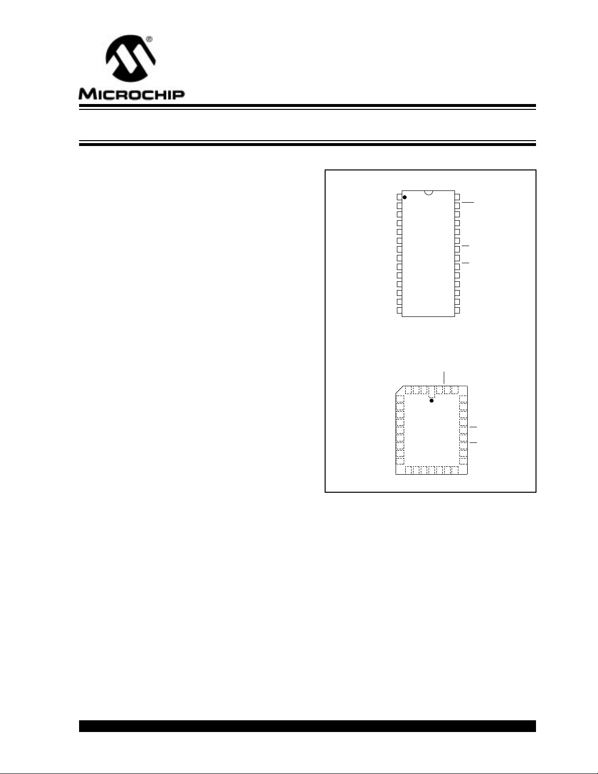
P ACKA GE TYPES
DIP/SOIC
• 1
V
PP
A12
2
A7
3
A6
4
A5
5
A4
6
A3
7
A2
8
A1
9
A0
10
O0
11
O1
12
O2
13
V
14
SS
PLCC
A7
432
5
A6
6
A5
7
A4
8
A3
9
A2
10
A1
11
A0
12
NC
13
O0
14
O1
A12
15
O2
16
27C64
PP
V
NU
Vcc
1
32
27C64
17
18
SS
O3
NU
V
28
27
26
25
24
23
22
21
20
19
18
17
16
15
PGM
31
19
O4
30
20
NC
O5
V
CC
PGM
NC
A8
A9
A11
OE
A10
CE
O7
O6
O5
O4
O3
29
28
27
26
25
24
23
22
21
A8
A9
A11
NC
OE
A10
CE
O7
O6
1996 Microchip Technology Inc. DS11107L-page 1
27C64
µ
µ
µ
±
µ
1.0 ELECTRICAL CHARA CTERISTICS
1.1 Maxim
CC
V
and input voltages w.r.t. V
voltage w.r.t. V
PP
V
um Ratings*
during
SS
SS
.......-0.6V to + 7.25V
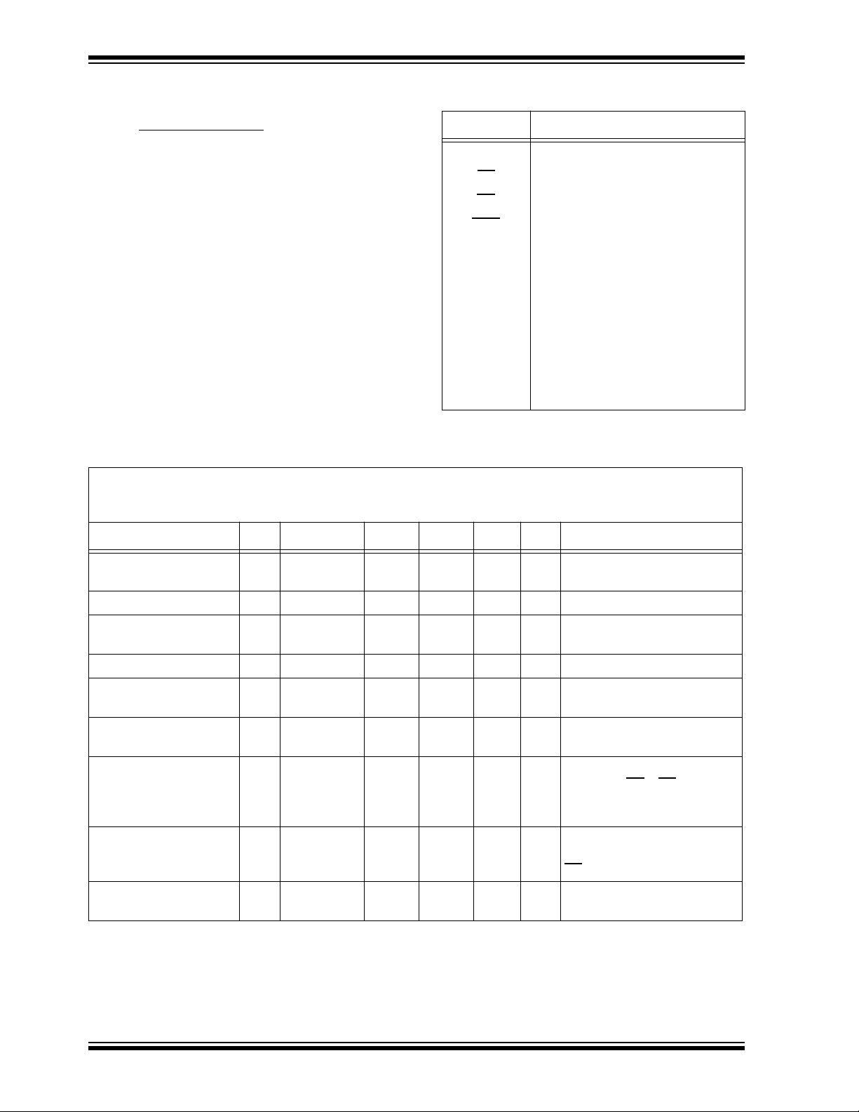
TABLE 1-1: PIN FUNCTION TABLE
A0-A12 Address Inputs
programming..........................................-0.6V to +14V
Voltage on A9 w.r.t. V
Output voltage w.r.t. V
......................-0.6V to +13.5V
SS
SS
............... -0.6V to V
CC
+1.0V
Storage temperature ..........................-65˚C to +150˚C
Ambient temp. with power applied .....-65˚C to +125˚C
*Notice: Stresses above those listed under “Maximum Ratings”
may cause permanent damage to the device. This is a stress rating only and functional operation of the device at those or any
other conditions above those indicated in the operation listings of
this specification is not implied. Exposure to maximum rating conditions for extended periods may affect device reliability.
O0 - O7 Data Output
TABLE 1-2: READ OPERATION DC CHARACTERISTICS
CC
V
= +5V ( ± 10%)
Commercial: Tamb = 0˚C to +70˚C
Industrial: Tamb = -40˚C to +85˚C
Name Function
CE
OE
PGM
PP
V
V
CC
V
SS
Chip Enable
Output Enable
Program Enable
Programming Voltage
+5V Power Supply
Ground
NC No Connection; No Internal Connec-
tions
NU Not Used; No External Connection Is
Allowed
Parameter Part* Status Symbol Min Max Units Conditions
Input Voltages all Logic "1"
Logic "0"
Input Leakage all — I
Output Voltages all Logic "1"
Logic "0"
Output Leakage all — I
Input Capacitance all — C
V
IH
IL
V
LI
V
OH
OL
V
LO
IN
2.0
V
+1
CC
-0.5
0.8
-10 10
V
V
AV
2.4
0.45VV
-10 10
AV
— 6 pF V
IN
= 0 to V
I
= -400 µ A
OH
I
OL
= 2.1 mA
OUT
= 0V; Tamb = 25 ° C;
IN
CC
= 0V to V
CC
f = 1 MHz
Output Capacitance all — C
OUT
—12pFV
OUT
= 0V; Tamb = 25 ° C;
f = 1 MHz
Power Supply Current,
Active
Power Supply Current,
Standby
PP
I
Read Current
PP
V
Read Voltage
* Parts: C=Commercial Temperature Range; I =Industrial Temperature Range.
C
I
C
I
all
all
all
TTL input
TTL input
TTL input
TTL input
CMOS input
Read Mode
Read Mode
CC1
I
CC2
I
I
(
CC
S
—
—
PP
I
PP
V
—
—
)
—
—
—
CC
V
-0.7
2025mAmAV
2
mA
3
mA
100
100
CC
V
CC
f = 1 MHz; OE
I
OUT
V
= 2.0 to V
IH
ACE
AVV
= V
PP
= 5.5V
= 5.5V; V
= 0 mA; V
CC
0.2V
PP
CC
= V
= CE = V
= -0.1 to 0.8V;
IL
; Note 1
CC
Note 1: Typical active current increases .5 mA per MHz up to operating frequency for all temperature ranges.
;
IL
;
DS11107L-page 2
1996 Microchip Technology Inc.
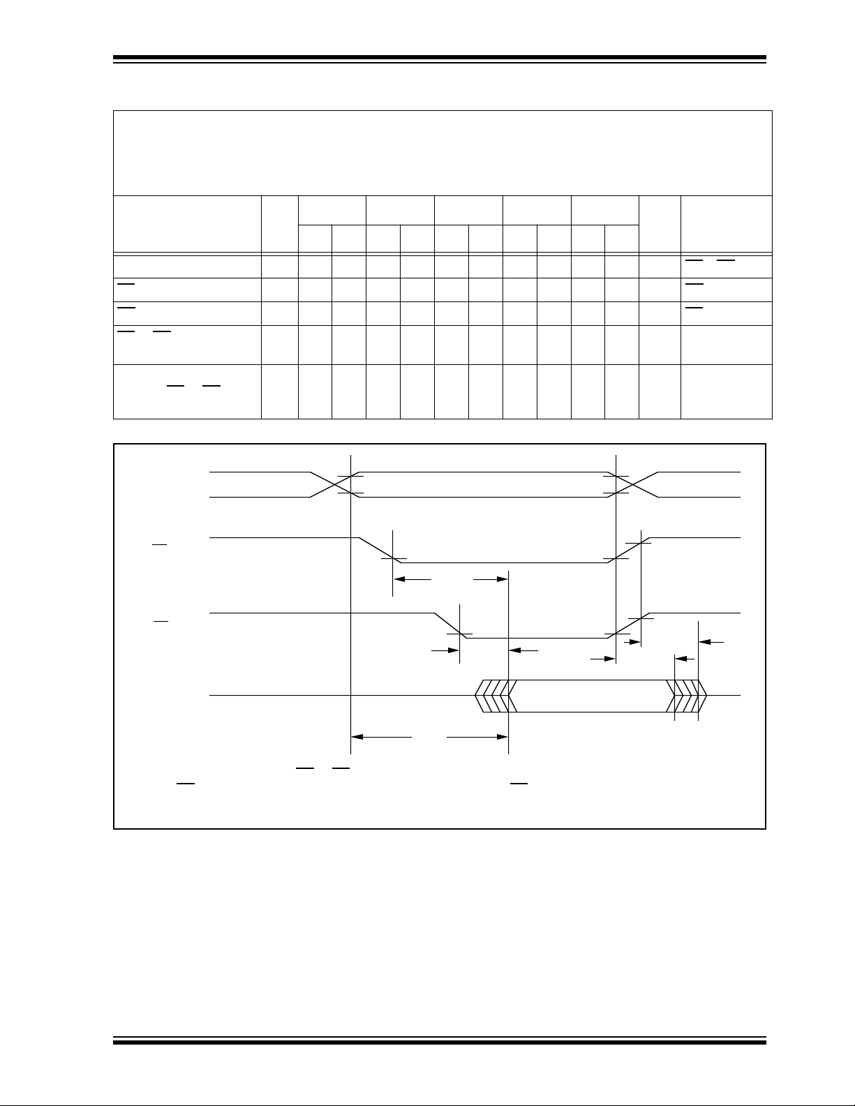
TABLE 1-3: READ OPERATION AC CHARACTERISTICS
27C64
AC Testing Waveform: V
Output Load: 1 TTL Load + 100 pF
Input Rise and Fall Times: 10 ns
Ambient Temperature: Commercial: Tamb = 0˚C to +70˚C
27C64-12 27C64-15 27C64-17 27C64-20 27C64-25
Parameter Sym
Min Max Min Max Min Max Min Max Min Max
Address to Output Delay t
to Output Delay t
CE
to Output Delay t
OE
or OE to O/P High
CE
ACC
— 120 — 150 — 170 — 200 — 250 ns CE = OE = V
CE
— 120 — 150 — 170 — 200 — 250 ns OE
OE
—65—70—70—75—100nsCE
t
OFF
050050050055060ns
Impedance
Output Hold from
OH
t
0—0—0—0—0—ns
Address CE or OE,
whichever occurs first
FIGURE 1-1: READ WAVEFORMS
V
IH
Address
VIL
IH
= 2.4V and V
IL
= 0.45V; V
OH
= 2.0V V
OL
= 0.8V
Industrial: Tamb = -40˚C to +85˚C
Units Conditions
Address Valid
= V
= V
IL
IL
IL
VIH
CE
VIL
tCE(2)
VIH
OE
Outputs
O0 - O7
VIL
V
VOL
OH
High Z
tOE(2)
tACC
Note 1: tOFF is specified for OE or CE, whichever occurs first.
2: OE
may be delayed up to tCE - tOE after the falling edge of CE without impact on tCE.
3: This parameter is sampled and is not 100% tested.
Valid Output
tOFF(1,3)
tOH
High Z
1996 Microchip Technology Inc. DS11107L-page 3
27C64
TABLE 1-4: PROGRAMMING DC CHARACTERISTICS
Ambient Temperature: Tamb = 25 ° C ± 5 ° C
CC
V
= 6.5V ± 0.25V, V
Parameter Status Symbol Min Max. Units Conditions
PP
H
= V
= 13.0V ± 0.25V
µ
Input Voltages Logic”1”
Logic”0”
Input Leakage — I
Output Voltages Logic”1”
Logic”0”
V
Current, program & verify — I
CC
V
PP
Current, program — I
A9 Product Identification — V
Note 1: V
CC
must be applied simultaneously or before V
V
V
V
V
CC2
PP2
IH
LI
OH
OL
2.0
V
CC
+1
IL
-0.1
0.8
-10 10
2.4
——0.45
V
V
AV
IN
VVI
OH
I
OL
= 0V to V
= -400 µ A
= 2.1 mA
CC
— 20 mA Note 1
— 25 mA Note 1
H
11.5 12.5 V
PP
and removed simultaneously or after V
PP
.
TABLE 1-5: PROGRAMMING AC CHARACTERISTICS
=2.4V and V
for Program, Program Verify AC Testing Waveform: V
IH
and Program Inhibit Modes Ambient Temperature: Tamb=25 ° C
V
CC= 6.5V ± 0.25V, VPP = VH = 13.0V ± 0.25V
Parameter Symbol Min Max Units Remarks
Address Set-Up Time t
Data Set-Up Time t
Data Hold Time t
Address Hold Time t
Float Delay (2) t
CC Set-Up Time tVCS 2—µs
V
Program Pulse Width (1) t
Set-Up Time tCES 2—µs
CE
Set-Up Time tOES 2—µs
OE
PP Set-Up Time tVPS 2—µs
V
Data Valid from OE
AS 2—µs
DS 2—µs
DH 2—µs
AH 0—µs
DF 0 130 ns
PW 95 105 µs 100 µs typical
tOE — 100 ns
Note 1: For express algorithm, initial programming width tolerance is 100 µs ±5%.
2: This parameter is only sampled and not 100% tested. Output float is defined as the point where data is no
longer driven (see timing diagram).
±5°C
=0.45V; V
IL
=2.0V; V
OH
OL
=0.8V
DS11107L-page 4
1996 Microchip Technology Inc.
 Loading...