

Microchip Technology Inc 25LC640XT-I-ST, 25LC640XT-ST, 25LC640X-I-ST, 25LC640X-ST, 25LC640T-I-ST Datasheet
...
1997 Microchip Technology Inc.
Preliminary
DS21223A-page 1
M
25AA640/25LC640/25C640
DEVICE SELECTION TABLE
FEATURES
• Low power CMOS technology
- Write current: 3 mA typical
- Read current: 500 µ A typical
- Standby current: 500 nA typical
• 8192 x 8 bit organization
• 32 byte page
• Write cycle time: 5ms max.
• Self-timed ERASE and WRITE cycles
• Block write protection
- Protect none, 1/4, 1/2, or all of array
• Built-in write protection
- Power on/off data protection circuitry
- Write enable latch
- Write protect pin
• Sequential read
• High reliability
- Endurance: 1M cycles (guaranteed)
- Data retention: > 200 years
- ESD protection: > 4000 V
• 8-pin PDIP, SOIC, and TSSOP packages
• Temperature ranges supported:
DESCRIPTION
The Microchip Technology Inc. 25AA640/25LC640/
25C640 (25xx640
*
) is a 64K bit serial Electrically Erasable PROM. The memory is accessed via a simple
Serial Peripheral Interface (SPI) compatible serial bus.
The bus signals required are a clock input (SCK) plus
separate data in (SI) and data out (SO) lines. Access to
the device is controlled through a chip select (CS
) input.
Communication to the device can be paused via the
hold pin (HOLD
). While the device is paused, transitions on its inputs will be ignored, with the exception of
chip select, allowing the host to service higher priority
interrupts.
PACKAGE TYPES
BLOCK DIAGRAM
Part
Number
V
CC
Range
Max Clock
Frequency
Temp
Ranges
25AA640 1.8-5.5V 1 MHz C,I
25LC640 2.5-5.5V 2 MHz C,I
25C640 4.5-5.5V 3 MHz C,I,E
- Commercial: (C) 0 ° C to +70 ° C
- Industrial: (I) -40 ° C to +85 ° C
- Automotive: (E) (25C640) -40 ° C to +125 ° C
25xx640
TSSOP
1
2
3
4
8
7
6
5
SCK
SI
V
SS
WP
HOLD
VCC
CS
SO
25xx640
PDIP/SOIC
1
2
3
4
8
7
6
5
V
CC
HOLD
SCK
SI
CS
SO
WP
VSS
SI
SO
SCK
CS
HOLD
WP
Status
Register
I/O Control
Memory
Control
Logic
X
Dec
HV Generator
EEPROM
Array
Page Latches
Y Decoder
Sense Amp.
R/W Control
Logic
VCC
VSS
64K SPI
™
Bus Serial EEPROM
*25xx640 is used in this document as a generic part number for the 25AA640/25LC640/25C640 devices.
SPI is a trademark of Motorola.
25AA640/25LC640/25C640
DS21223A-page 2
Preliminary
1997 Microchip Technology Inc.
1.0 ELECTRICAL
CHARACTERISTICS
1.1 Maxim
um Ratings*
Vcc...................................................................................7.0V
All inputs and outputs w.r.t. Vss.................. -0.6V to Vcc+1.0V
Storage temperature.......................................-65˚C to 150˚C
Ambient temperature under bias..................... -65˚C to 125˚C
Soldering temperature of leads (10 seconds).............+300˚C
ESD protection on all pins.................................................4kV
*Notice: Stresses above those listed under ‘Maximum ratings’ may
cause permanent damage to the device. This is a stress rating only and
functional operation of the device at those or any other conditions
above those indicated in the operational listings of this specification is
not implied. Exposure to maximum rating conditions for an extended
period of time may affect device reliability
TABLE 1-1: PIN FUNCTION TABLE
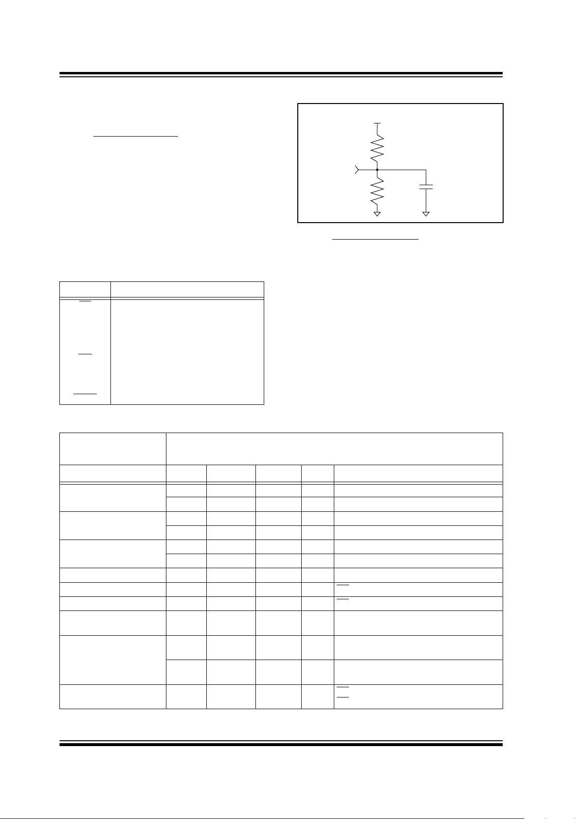
FIGURE 1-1: AC TEST CIRCUIT
1.2 A
C Test Conditions
Name Function
CS
Chip Select Input
SO Serial Data Output
SI Serial Data Input
SCK Serial Clock Input
WP
Write Protect Pin
V
SS
Ground
V
CC
Supply Voltage
HOLD
Hold Input
AC Waveform:
V
LO
= 0.2V
V
HI
= V
CC
- 0.2V (Note 1)
V
HI
= 4.0V (Note 2)
Timing Measurement Reference Level
Input 0.5 V
CC
Output 0.5 V
CC
Note 1: For V
CC
≤
4.0V
2:
For V
CC
> 4.0V
VCC
SO
100 pF
1.8 K
2.25 K
TABLE 1-2: DC CHARACTERISTICS
All parameters apply over the
specified operating ranges
unless otherwise noted.
Commercial (C): Tamb = 0 ° C to +70 ° C
V
CC
= 1.8V to 5.5V
Industrial (I): Tamb = -40 ° C to +85 ° C V
CC
= 1.8V to 5.5V
Automotive (E): Tamb = -40 ° C to +125 ° C V
CC
= 4.5V to 5.5V (25C640 only)
Parameter Symbol Min Max Units Test Conditions
High level input voltage
V
IH
1 2.0 V
CC
+1 V V
CC
≥ 2.7V (Note)
V
IH
2 0.7 V
CC
V
CC
+1 V V
CC
< 2.7V (Note)
Low level input voltage
V
IL
1 -0.3 0.8 V V
CC
≥ 2.7V (Note)
V
IL
2 -0.3 0.3 V
CC
V V
CC
< 2.7V (Note)
Low level output voltage
V
OL
— 0.4 V I
OL
= 2.1 mA
V
OL
— 0.2 V I
OL
= 1.0 mA, V
CC
< 2.5V
High level output voltage V
OH
V
CC
-0.5 — V I
OH
=-400 µ A
Input leakage current I
LI
-10 10
µ
A CS
= V
CC
, V
IN
= V
SS
TO
V
CC
Output leakage current I
LO
-10 10
µ
A CS
= V
CC
, V
OUT
= V
SS
TO
V
CC
Internal Capacitance
(all inputs and outputs)
C
INT
— 7 pF T
AMB
= 25˚C, CLK = 1.0 MHz,
V
CC
= 5.0V (Note)
Operating Current
I
CC
Read —
—
1
500
mA
µ
A
V
CC
= 5.5V; F
CLK
=3.0 MHz; SO = Open
V
CC
= 2.5V; F
CLK
=2.0 MHz; SO = Open
I
CC
Write —
—
5
3
mAmAV
CC
= 5.5V
V
CC
= 2.5V
Standby Current I
CCS
—
—
5
1
µ A µ
A
CS
= Vcc = 5.5V, Inputs tied to V
CC
or V
SS
CS = Vcc = 2.5V, Inputs tied to V
CC
or V
SS
Note: This parameter is periodically sampled and not 100% tested.
25AA640/25LC640/25C640
1997 Microchip Technology Inc.
Preliminary
DS21223A-page 3
TABLE 1-3: AC CHARACTERISTICS
All parameters apply over the
specified operating ranges
unless otherwise noted.
Commercial (C): Tamb = 0 ° C to +70 ° C V
CC
= 1.8V to 5.5V
Industrial (I): Tamb = -40 ° C to +85 ° C V
CC
= 1.8V to 5.5V
Automotive (E): Tamb = -40 ° C to +125°C V
CC = 4.5V to 5.5V (25C640 only)
Parameter Symbol Min Max Units Test Conditions
Clock Frequency FCLK —
—
—
3
2
1
MHz
MHz
MHz
VCC = 4.5V to 5.5V
VCC = 2.5V to 4.5V
VCC = 1.8V to 2.5V
CS Setup Time TCSS 100
250
500
—
—
—
ns
ns
ns
VCC = 4.5V to 5.5V
VCC = 2.5V to 4.5V
VCC = 1.8V to 2.5V
CS Hold Time TCSH 150
250
475
—
—
—
ns
ns
ns
VCC = 4.5V to 5.5V
VCC = 2.5V to 4.5V
VCC = 1.8V to 2.5V
CS Disable Time TCSD 500 — ns
Data Setup Time TSU 30
50
50
—
—
—
ns
ns
ns
VCC = 4.5V to 5.5V
VCC = 2.5V to 4.5V
VCC = 1.8V to 2.5V
Data Hold Time THD 50
100
100
—
—
—
ns
ns
ns
VCC = 4.5V to 5.5V
VCC = 2.5V to 4.5V
VCC = 1.8V to 2.5V
CLK Rise Time TR — 2 µs (Note 1)
CLK Fall Time TF — 2 µs (Note 1)
Clock High Time THI 150
250
475
—
—
—
ns
ns
ns
VCC = 4.5V to 5.5V
VCC = 2.5V to 4.5V
VCC = 1.8V to 2.5V
Clock Low Time TLO 150
250
475
—
—
—
ns
ns
ns
VCC = 4.5V to 5.5V
VCC = 2.5V to 4.5V
V
CC = 1.8V to 2.5V
Clock Delay Time TCLD 50 — ns
Clock Enable Time TCLE 50 — ns
Output Valid from
Clock Low
TV —
—
—
150
250
475
ns
ns
ns
VCC = 4.5V to 5.5V
VCC = 2.5V to 4.5V
VCC = 1.8V to 2.5V
Output Hold Time THO 0 — ns (Note 1)
Output Disable Time TDIS —
—
—
200
250
500
ns
ns
ns
VCC = 4.5V to 5.5V (Note 1)
VCC = 2.5V to 4.5V (Note 1)
VCC = 1.8V to 2.5V (Note 1)
HOLD Setup Time THS 100
100
200
—
—
—
ns
ns
ns
VCC = 4.5V to 5.5V
VCC = 2.5V to 4.5V
VCC = 1.8V to 2.5V
HOLD Hold Time THH 100
100
200
—
—
—
ns
ns
ns
VCC = 4.5V to 5.5V
VCC = 2.5V to 4.5V
VCC = 1.8V to 2.5V
HOLD Low to Output High-Z THZ 100
150
200
—
—
—
ns
ns
ns
VCC = 4.5V to 5.5V (Note 1)
VCC = 2.5V to 4.5V (Note 1)
VCC = 1.8V to 2.5V (Note 1)
HOLD High to Output Valid THV 100
150
200
—
—
—
ns
ns
ns
VCC = 4.5V to 5.5V
VCC = 2.5V to 4.5V
VCC = 1.8V to 2.5V
Internal Write Cycle Time TWC — 5 ms
Endurance — 1M — E/W Cycles (Note 2)
Note 1: This parameter is periodically sampled and not 100% tested.
2: This parameter is not tested but guaranteed by characterization. For endurance estimates in a specific application, please
consult the Total Endurance Model which can be obtained on Microchip’s BBS or website.
25AA640/25LC640/25C640
DS21223A-page 4 Preliminary 1997 Microchip Technology Inc.
FIGURE 1-2: HOLD TIMING
FIGURE 1-3: SERIAL INPUT TIMING
FIGURE 1-4: SERIAL OUTPUT TIMING
CS
SCK
SO
SI
HOLD
THH
THS THS THH
THVTHZ
don’t care
TSU
high impedance
n+2 n+1 n n-1
n
n+2 n+1 n
n
n-1
CS
SCK
SI
SO
TCSS
THDTsu
TF
TR
TCSD
TCLD
TCSH
LSB in
MSB in
high impedance
TCLE
Mode 1,1
Mode 0,0
CS
SCK
SO
TLO
THI
THO
TV
MSB out
LSB out
TCSH
TDIS
don’t care
SI
Mode 1,1
Mode 0,0
 Loading...