

Microchip Technology Inc 25C320T-I-ST, 25C320T-I-SN, 25C320T-I-P, 25C320T-E-ST, 25C320T-E-SN Datasheet
...
1996 Microchip Technology Inc.
Preliminary
DS21159B-page 1
FEATURES
• SPI modes 0,0 and 1,1
• 3.0 MHz Clock Rate
• Single 5V Supply
• Low Power CMOS Technology
- Max Write Current: 5 mA
- Read Current: 1.0 mA at 5.5V, 3MHz
- Standby Current: 1 µ A typical
• 4096 x 8 Organization
• 32 Byte Page
• Sequential Read
• Self-timed ERASE and WRITE Cycles
• Block Write Protection
- Protect none, 1/4, 1/2, or all of Array
• Built-in Write Protection
- Power On/Off Data Protection Circuitry
- Write Enable Latch
- Write Protect Pin
• High Reliability
- Endurance: 1M cycles (guaranteed)
- Data Retention: >200 years
- ESD protection: >4000V
• 8-pin PDIP/SOIC, 14-pin TSSOP
• Temperature ranges supported
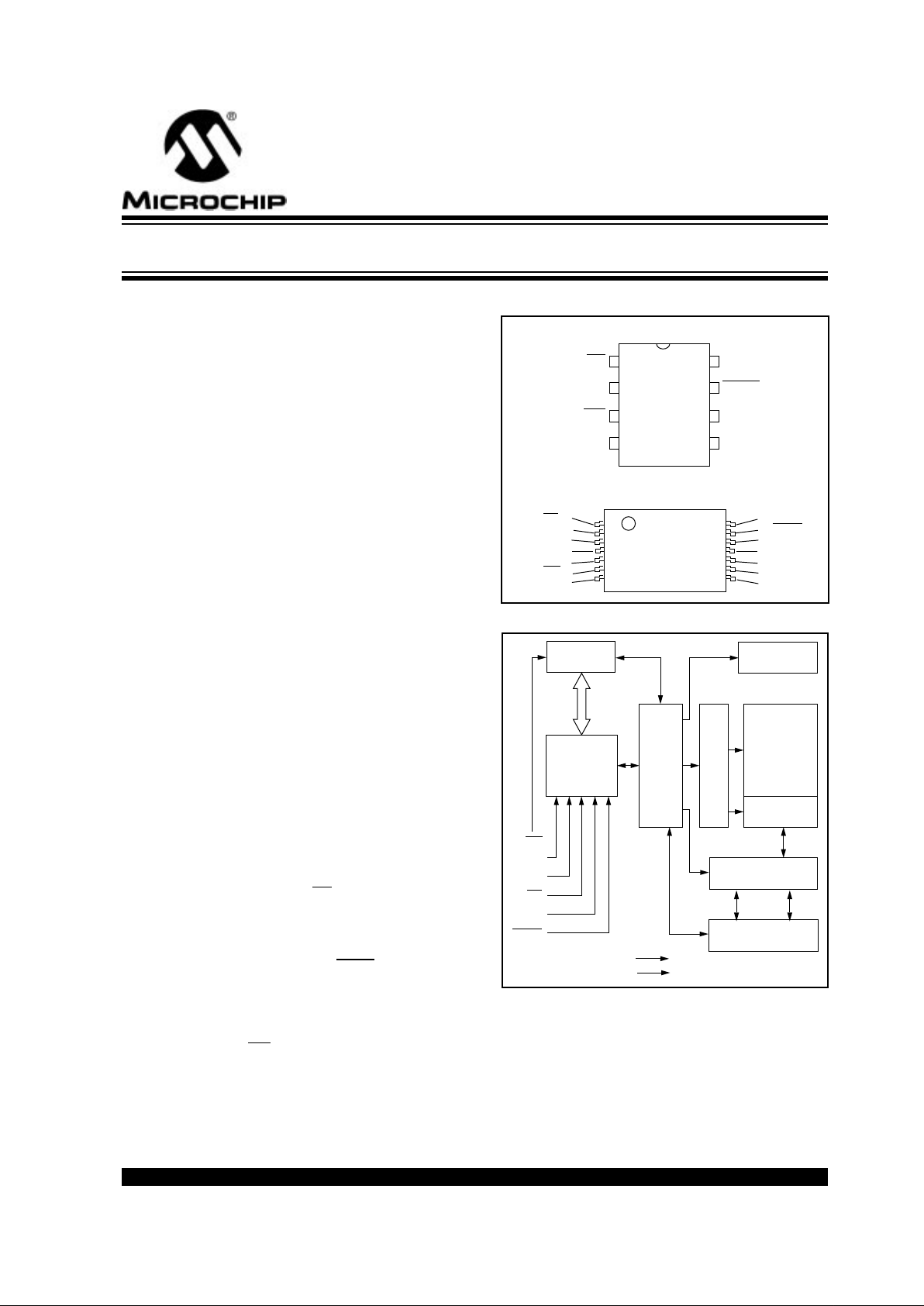
DESCRIPTION
The Microchip Technology Inc. 25C320 is a 32K-bit
serial Electrically Erasable PROM (EEPROM). The
memory is accessed via a simple Serial Peripheral
Interface (SPI) compatible serial bus. The bus signals
required are a clock input (SCK) plus separate data in
(SI) and data out (SO) lines. Access to the device is
controlled through a chip select (CS
) input, allowing any
number of devices to share the same bus.
There are two other inputs that provide the end user
with additional flexibility. Communication to the device
can be paused via the hold pin (HOLD
). While the
device is paused, transitions on its inputs will be
ignored, with the exception of chip select, allowing the
host to service higher priority interrupts. Also write
operations to the Status Register can be disabled via
the write protect pin (WP
).
- Commercial (C): 0 ° C to +70 ° C
- Industrial (I): -40 ° C to +85 ° C
- Automotive (E): -40 ° C to +125 ° C
PACKAGE TYPES
BLOCK DIAGRAM
DIP/SOIC
25C320
CS
SO
WP
VSS
1
2
3
4
8
7
6
5
VCC
HOLD
SCK
SI
25C320
14
13
12
11
10
9
8
VCC
HOLD
NC
NC
NC
SCK
SI
1
2
3
4
5
6
7
CS
SO
NC
NC
NC
WP
VSS
TSSOP
SI
SO
SCK
CS
HOLD
WP
Status
Register
I/O Control
Memory
Control
Logic
X
Dec
HV Generator
EEPROM
Array
Page Latches
Y Decoder
Sense Amp.
R/W Control
Logic
Vcc
Vss
25C320
32K 5.0V SPI
Bus Serial EEPROM
SPI is a trademark of Motorola.
25C320
DS21159B-page 2
Preliminary
1996 Microchip Technology Inc.
1.0 ELECTRICAL
CHARACTERISTICS
1.1 Maxim
um Ratings*
V
CC
........................................................................7.0V
All inputs and outputs w.r.t. V
SS
.......-0.6V to V
CC
+1.0V
Storage temperature............................ -65 ° C to 150 ° C
Ambient temperature under bias..........-65 ° C to 125 ° C
Soldering temperature of leads
(10 seconds) .................................................... +300 ° C
ESD protection on all pins..................................... 4 kV
*Notice: Stresses above those listed under ‘Maximum ratings’
may cause permanent damage to the device. This is a stress rating only and functional operation of the device at those or any
other conditions above those indicated in the operational listings
of this specification is not implied. Exposure to maximum rating
conditions for extended period of time may affect device reliability
TABLE 1-1: PIN FUNCTION TABLE
Name Function
CS
Chip Select Input
SO Serial Data Output
SI Serial Data Input
SCK Serial Clock Input
WP
Write Protect Pin
V
SS
Ground
V
CC
Supply V oltage
HOLD
Hold Input
NC No Connect
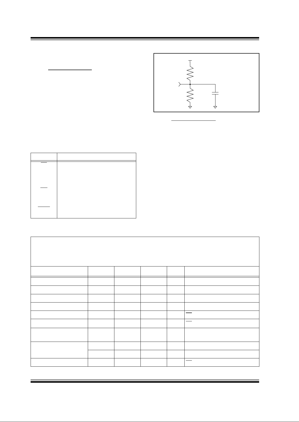
FIGURE 1-1: AC TEST CIRCUIT
1.2 A
C Test Conditions
AC Waveform:
V
LO
= 0.2V
V
HI
= Vcc - 0.2V
(Note 1)
V
HI
= 4.0V
(Note 2)
Timing Measurement Reference Level
Input 0.5 V
CC
Output 0.5 V
CC
Note 1: For V
CC
≤
4.0V
2: For V
CC
> 4.0V
Vcc
SO
100 pF
1.8 K
2.25 K
TABLE 1-2: DC CHARACTERISTICS
Applicable over recommended operating ranges shown below unless otherwise noted:
V
CC
= 4.5V to 5.5V
Commercial (C): Tamb = 0 ° C to +70˚C
Industrial (I): Tamb =-40˚C to +85˚C
Automotive (E): Tamb = -40 ° C to +125 ° C
Parameter Symbol Min Max Units Test Conditions
High level input voltage V
IH
2.0 V
CC
+1 V
Low level input voltage V
IL
-0.3 0.8 V
Low level output voltage V
OL
— 0.4 V I
OL
=2.1 mA
High level output voltage V
OH
V
CC
-0.5 — V I
OH
=-400 µ A
Input leakage current I
LI
-10 10
µ
ACS
=V
IH
, V
IN
=GND to V
CC
Output leakage current I
LO
-10 10
µ
ACS
=V
IH
, V
OUT
=GND to V
CC
Internal Capacitance
(all inputs and outputs)
C
INT
— 7 pF Tamb=25 ° C, F
CLK
=1.0 MHz,
V
CC
=5.5V (Note)
Operating Current I
CC write
—— 5 mA V
CC
=5.5V; SO=Open
I
CC
read
— 1 mA V
CC
=5.5V; SO=Open, F
CLK
=3.0 MHz
Standby Current I
CCS
—5
µ
ACS
=V
CC
=5.5V; V
IN
=Gnd or V
CC
Note: This parameter is periodically sampled and not 100% tested.
1996 Microchip Technology Inc.
Preliminary
DS21159B-page 3
25C320
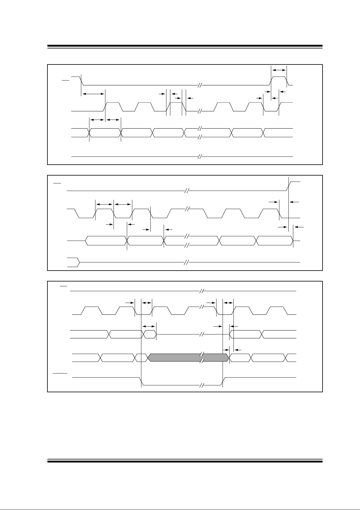
FIGURE 1-2: SERIAL
INPUT TIMING
FIGURE 1-3: SERIAL OUTPUT TIMING
FIGURE 1-4: HOLD TIMING
CS
SCK
SI
SO
t
CSS
t
HD
t
SU
t
F
t
R
t
CSD
t
CLD
t
CSH
lsb inmsb in
high impedance
CS
SCK
SO
t
LO
t
HI
t
HO
t
V
msb out
lsb out
t
CSH
t
DIS
don’t care
SI
CS
SCK
SO
SI
HOLD
t
HH
t
HS
t
HS
t
HH
t
HV
t
HZ
don’t care
t
SU
high impedance
n+2 n+1 n n-1
n
n+2 n+1 n
n
n-1
25C320
DS21159B-page 4
Preliminary
1996 Microchip Technology Inc.
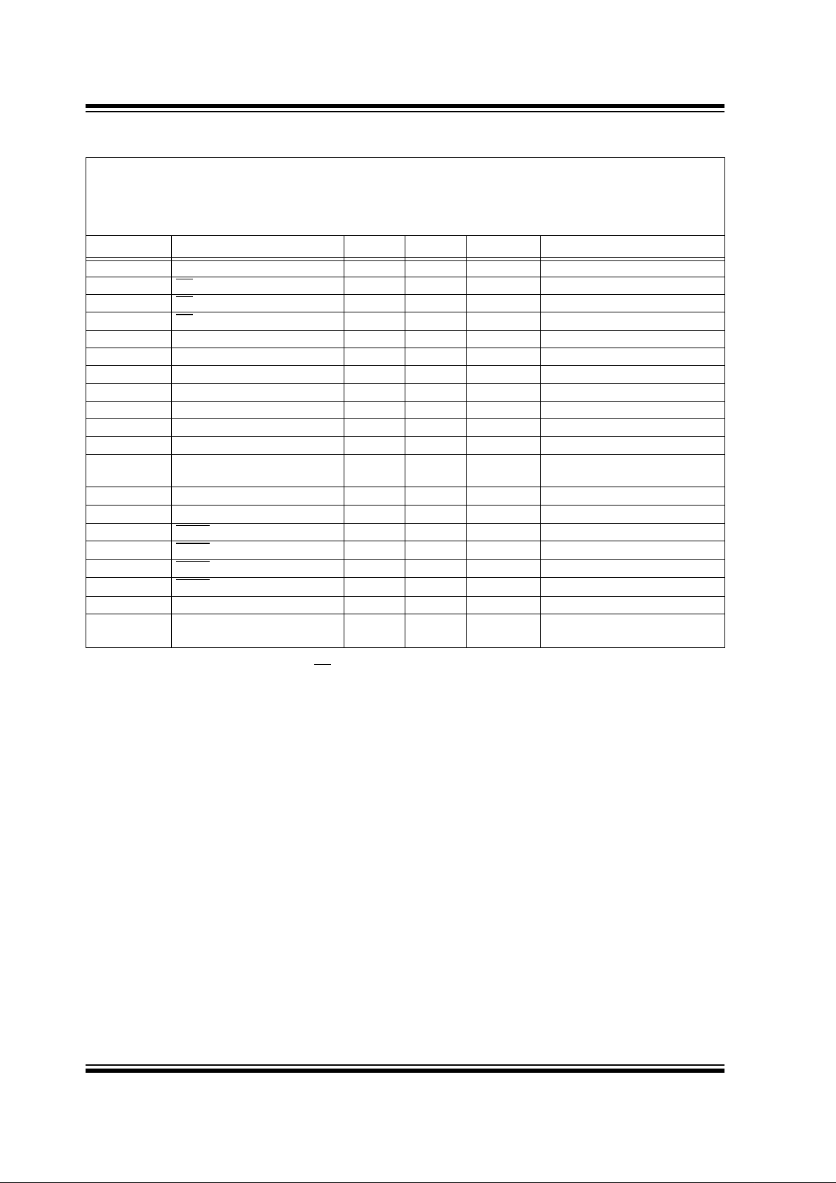
TABLE 1-3: AC CHARACTERISTICS
Applicable over recommended operating ranges shown below unless otherwise noted:
V
CC
= 4.5V to 5.5V
Commercial (C): Tamb = 0 ° C to +70 ° C
Industrial (I): Tamb = +40 ° C to +85C
Automotive (E): Tamb = -40 ° C to +125 ° C
Symbol Parameter Min Max Units Test Conditions
f
SCK Clock Frequency — 3 MHz
t
CSS CS Setup Time 100 — ns
t
CSH CS Hold Time 100 — ns
t
CSD CS Disable Time 250 — ns
t
SU Data Setup Time 30 — ns
t
HD Data Hold Time 50 — ns
t
R CLK Rise Time — 2 µs (Note 1)
t
F CLK Fall Time — 2 µs (Note 1)
t
HI Clock High Time 150 — ns
t
LO Clock Low Time 150 — ns
t
CLD Clock Delay Time 50 — ns
t
V Output V alid from
Clock Low
— 150 ns
t
HO Output Hold Time 0 — ns
t
DIS Output Disable Time — 200 ns
(Note 1)
t
HS HOLD Setup Time 100 — ns
t
HH HOLD Hold Time 100 — ns
t
HZ HOLD Low to Output High-Z 100 — ns
(Note 1)
t
HV HOLD High to Output Valid 100 — ns
(Note 1)
t
WC Internal Write Cycle Time — 5 ms (Note 2)
— Endurance 1M — E/W Cycles 25°C, Vcc = 5.0V, Block Mode
(Note 3)
Note 1: This parameter is periodically sampled and not 100% tested.
2: t
WC begins on the rising edge of CS after a valid write sequence and ends when the internal self-timed write
cycle is complete.
3: This parameter is not tested but guaranteed b y characterization. For endurance estimates in a specific appli-
cation, please consult the Total Endurance Model which can be obtained on our BBS or website.
 Loading...