

Microchip Technology Inc 24LC21AT-I-SN, 24LC21AT-I-P, 24LC21AT-P, 24LC21A-I-SN, 24LC21A-I-P Datasheet
...
1996 Microchip Technology Inc.
Preliminary
DS21160B-page 1
FEATURES
• Single supply with operation down to 2.5V
• Completely implements DDC1 /DDC2
interface for monitor identification, including recovery to DDC1
• Pin and function compatible with 24LC21
• Low power CMOS technology
- 1 mA typical active current
- 10 µ A standby current typical at 5.5V
• 2-wire serial interface bus, I
2
C
compatible
• 100 kHz (2.5V) and 400 kHz (5V) compatibility
• Self-timed write cycle (including auto-erase)
• Page-write buffer for up to eight bytes
• 10,000,000 erase/write cycles guaranteed
• Data retention > 200 years
• ESD Protection > 4000V
• 8-pin PDIP and SOIC package
• Available for extended temperature ranges
DESCRIPTION
The Microchip Technology Inc. 24LC21A is a 128 x 8bit dual-mode Electrically Erasable PROM. This device
is designed for use in applications requiring storage
and serial transmission of configuration and control
information. Two modes of operation have been implemented: Transmit-Only Mode and Bi-directional Mode.
Upon power-up, the device will be in the Transmit-Only
Mode, sending a serial bit stream of the memory array
from 00h to 7Fh, clocked by the VCLK pin. A valid high
to low transition on the SCL pin will cause the device to
enter the transition mode, and look for a valid control
byte on the I
2
C bus. If it detects a valid control byte from
the master, it will switch into Bi-directional Mode, with
byte selectable read/write capability of the memory
array using SCL. If no control byte is received, the
device will revert to the Transmit-Only Mode after it
receives 128 consecutive VCLK pulses while the SCL
pin is idle. The 24LC21A is available in a standard 8-pin
PDIP and SOIC package in both commercial and
industrial temperature ranges.
- Commercial (C): 0 ° C to +70 ° C
- Industrial (I): -40 ° C to +85 ° C
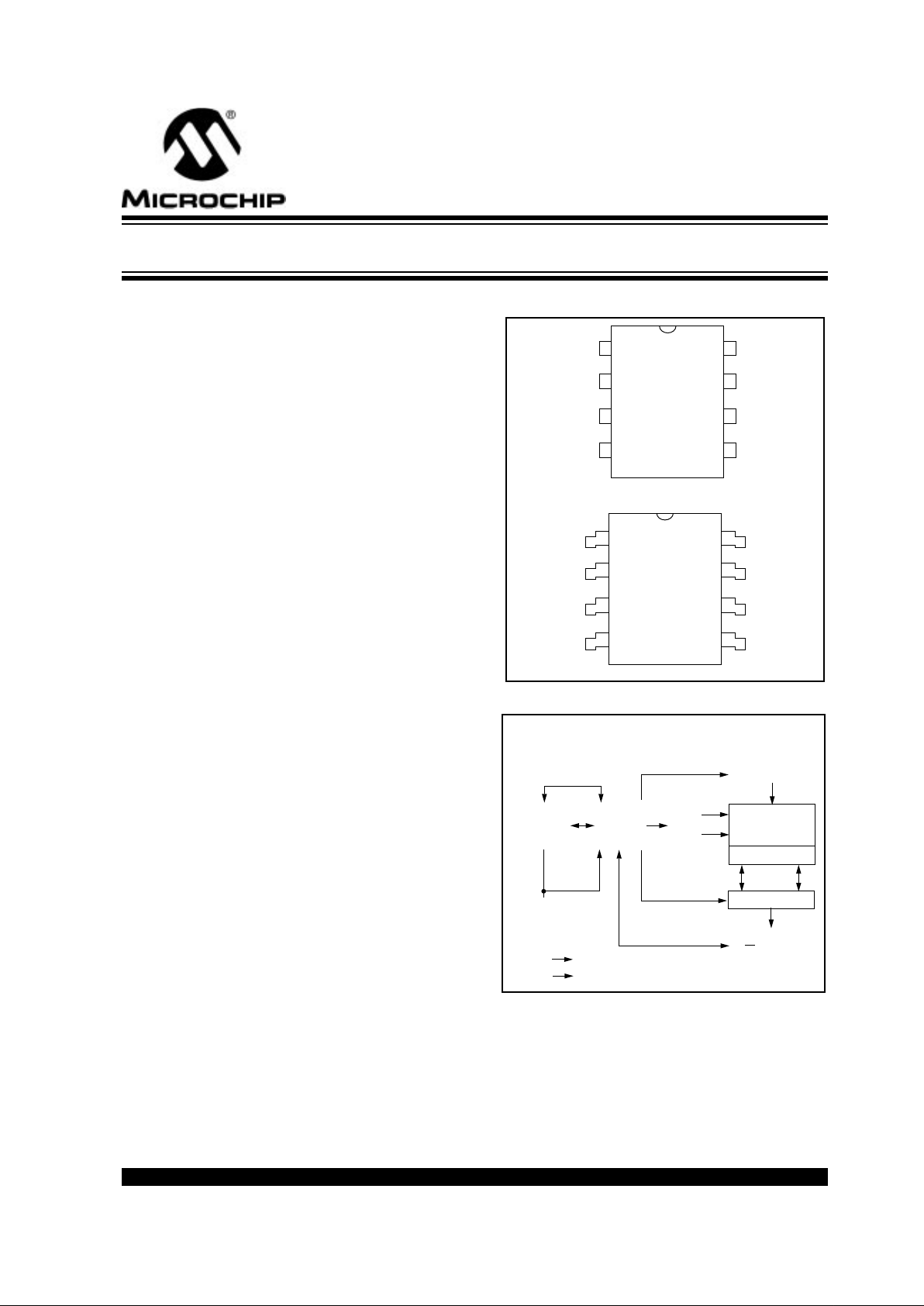
PACKA GE TYPES
BLOCK DIAGRAM
PDIP
SOIC
24LC21A
NC
NC
NC
V
SS
1
2
3
4
8
7
6
5
V
CC
VCLK
SCL
SDA
24LC21A
NC
NC
NC
V
SS
1
2
3
4
8
7
6
5
V
CC
VCLK
SCL
SDA
HV GENERATOR
EEPROM
ARRAY
PAGE LATCHES
YDEC
XDEC
SENSE AMP
R/W
CONTROL
MEMORY
CONTROL
LOGIC
I/O
CONTROL
LOGIC
SDA SCL
V
CC
VSS
VCLK
24LC21A
1K 2.5V Dual Mode I
2
C
Serial EEPROM
DDC is a trademark of the Video Electronics Standards Association.
I
2
C is a trademark of Philips Corporation.
24LC21A
DS21160B-page 2
Preliminary
1996 Microchip Technology Inc.
1.0 ELECTRICAL
CHARACTERISTICS
1.1 Maxim
um Ratings*
V
CC
........................................................................7.0V
All inputs and outputs w.r.t. V
SS
.... -0.6V to V
CC
+1.0V
Storage temperature ..........................-65 ° C to +150 ° C
Ambient temp. with power applied .....-65 ° C to +125 ° C
Soldering temperature of leads (10 seconds) ..+300 ° C
ESD protection on all pins .....................................≥ 4 kV
*
Notice: Stresses above those listed under “Maximum ratings” may cause perma-
nent damage to the device. This is a stress rating only and functional operation of
the device at those or any other conditions above those indicated in the operational
listings of this specification is not implied. Exposure to maximum rating conditions
for extended periods may affect device reliability.
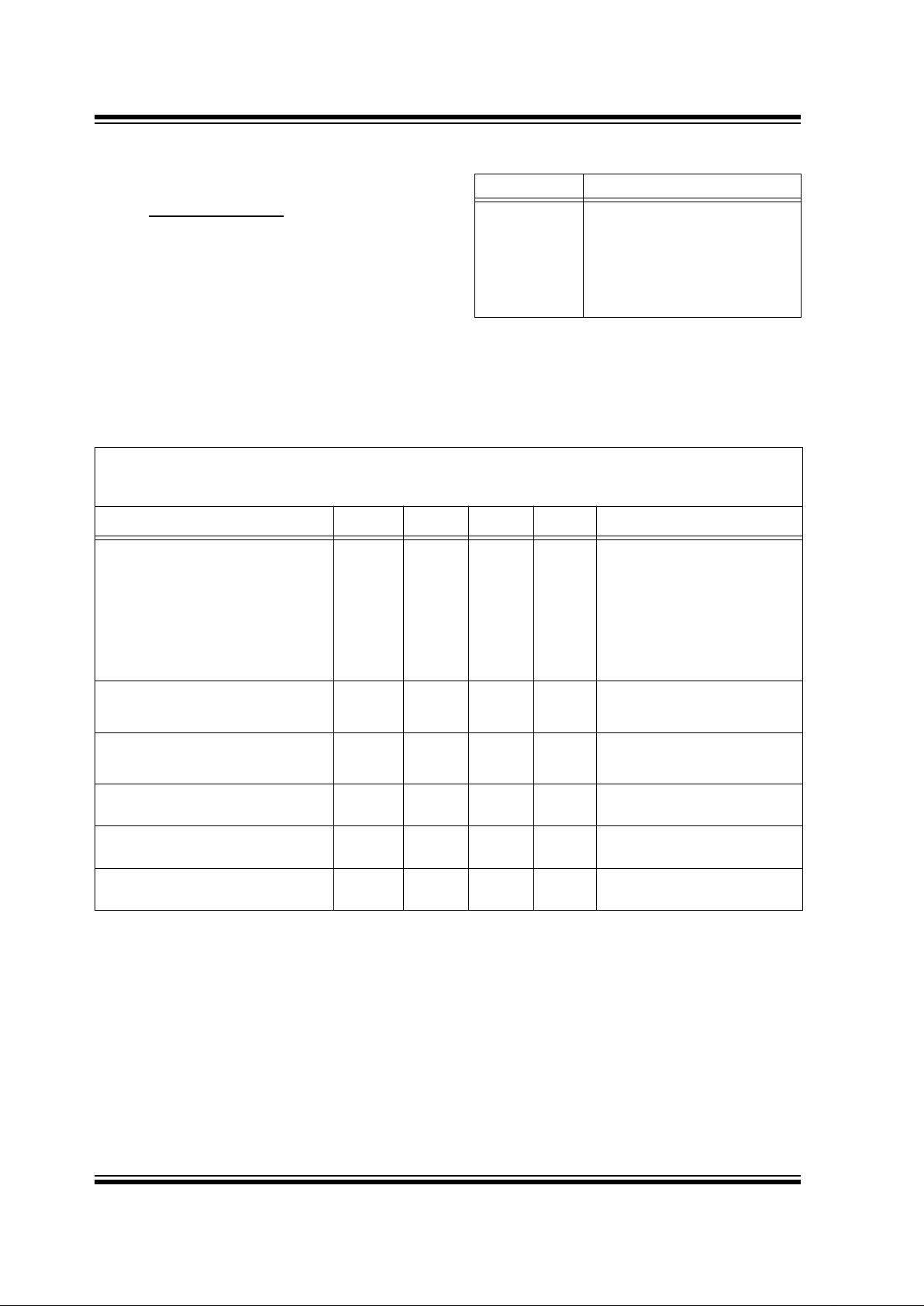
TABLE 1-1: PIN FUNCTION TABLE
Name Function
V
SS
Ground
SDA Serial Address/Data I/O
SCL Serial Clock (Bi-directional Mode)
VCLK Serial Clock (Transmit-Only Mode)
V
CC
+2.5V to 5.5V Power Supply
NC No Connection
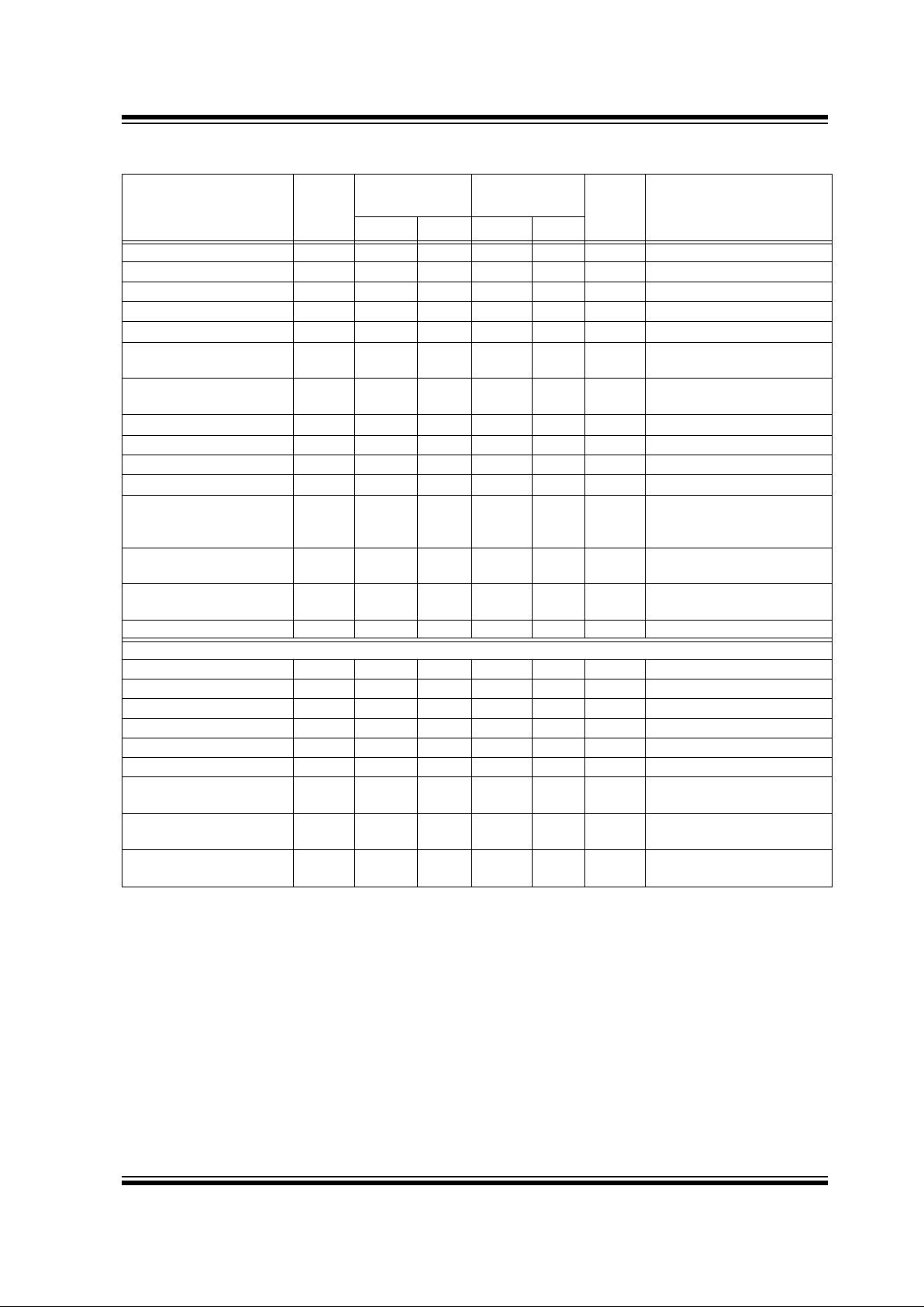
TABLE 1-2: DC CHARACTERISTICS
V
CC
= +2.5V to 5.5V
Commercial (C): Tamb = 0 ° C to +70 ° C
Industrial (I): Tamb =-40 ° C to +85 ° C
Parameter Symbol Min Max Units Conditions
SCL and SDA pins:
High level input voltage
Low level input voltage
V
IH
V
IL
0.7 V
CC
—
—
0.3 V
CC
V
V
Input levels on VCLK pin:
High level input voltage
Low level input voltage
V
IH
V
IL
2.0
—
—
0.2 V
CC
V
V
V
CC
≥
2.7V (Note)
V
CC
< 2.7V (Note)
Hysteresis of Schmitt trigger inputs V
HYS
.05 V
CC
— V (Note)
Low level output voltage V
OL1
— 0.4 V I
OL
= 3 mA, V
CC
= 2.5V (Note)
Low level output voltage V
OL2
— 0.6 V I
OL
= 6 mA, V
CC
= 2.5V
Input leakage current I
LI
-10 10
µ
AV
IN
= 0.1V to V
CC
Output leakage current I
LO
-10 10
µ
AV
OUT
= 0.1V to V
CC
Pin capacitance (all inputs/outputs) Cin, Cout — 10 pF V
CC
= 5.0V (Note)
Tamb = 25 ° C, F
CLK
= 1 MHz
Operating current I
CC
Write
I
CC
Read
—
—
3
1
mAmAV
CC
= 5.5V
V
CC
= 5.5V, SCL = 400 kHz
Standby current I
CCS
—
—
30
100
µ A µ
A
V
CC
= 3.0V, SDA = SCL = V
CC
V
CC
= 5.5V, SDA = SCL = V
CC
Note: This parameter is periodically sampled and not 100% tested.
1996 Microchip Technology Inc.
Preliminary
DS21160B-page 3
24LC21A
TABLE 1-3: AC CHARACTERISTICS
Parameter Symbol
Vcc= 2.5-5.5V
Standard Mode
Vcc= 4.5 - 5.5V
Fast Mode
Units Remarks
Min Max Min Max
Clock frequency F
CLK
— 100 — 400 kHz
Clock high time T
HIGH
4000 — 600 — ns
Clock low time T
LOW
4700 — 1300 — ns
SDA and SCL rise time T
R
— 1000 — 300 ns
(Note 1)
SDA and SCL fall time T
F
— 300 — 300 ns
(Note 1)
START condition hold time T
HD
:
STA
4000 — 600 — ns After this period the first clock
pulse is generated
START condition setup
time
T
SU
:
STA
4700 — 600 — ns Only relevant for repeated
START condition
Data input hold time T
HD
:
DAT
0—0—ns
(Note 2)
Data input setup time T
SU
:
DAT
250 — 100 — ns
STOP condition setup time T
SU
:
STO
4000 — 600 — ns
Output valid from clock T
AA
— 3500 — 900 ns
(Note 2)
Bus free time T
BUF
4700 — 1300 — ns Time the bus must be free
before a new transmission
can start
Output fall time from V
IH
minimum to V
IL
maximum
T
OF
— 250 20 +
0.1 C
B
250 ns
(Note 1), C
B
≤
100 pF
Input filter spike suppression (SDA and SCL pins)
T
SP
— 50 — 50 ns
(Note 3)
Write cycle time T
WR
— 10 — 10 ms Byte or Page mode
Transmit-Only Mode Parameters
Output valid from VCLK T
VAA
— 2000 — 1000 ns
VCLK high time T
VHIGH
4000 — 600 — ns
VCLK low time TVLOW 4700 — 1300 — ns
VCLK setup time T
VHST 0—0—ns
VCLK hold time T
SPVL 4000 — 600 — ns
Mode transition time T
VHZ — 1000 — 500 ns
Transmit-Only power up
time
T
VPU 0—0—ns
Input filter spike suppression (VCLK pin)
T
SPV — 100 — 100 ns
Endurance — 10M — 10M — cycles 25°C, Vcc = 5.0V , Block Mode
(Note 4)
Note 1: Not 100% tested. C
B = Total capacitance of one bus line in pF.
2: As a transmitter , the device must provide an internal minimum delay time to bridge the undefined region (min-
imum 300 ns) of the falling edge of SCL to avoid unintended generation of START or STOP conditions.
3: The combined T
SP and VHYS specifications are due to Schmitt trigger inputs which provide noise and spike
suppression. This eliminates the need for a T
I specification for standard operation.
4: This parameter is not tested but guaranteed by characterization. For endurance estimates in a specific appli-
cation, please consult the Total Endurance Model which can be obtained on our BBS or website.
24LC21A
DS21160B-page 4 Preliminary 1996 Microchip Technology Inc.
2.0 FUNCTIONAL DESCRIPTION
The 24LC21A is designed to comply to the DDC Standard proposed by VESA (Figure 3-3) with the exception
that it is not Access.bus capable. It operates in two
modes, the Transmit-Only Mode and the Bi-directional
Mode. There is a separate 2-wire protocol to support
each mode, each having a separate clock input but
sharing a common data line (SDA). The device enters
the Transmit-Only Mode upon power-up. In this mode,
the device transmits data bits on the SDA pin in
response to a clock signal on the VCLK pin. The device
will remain in this mode until a valid high to low transition is placed on the SCL input. When a valid transition
on SCL is recognized, the device will switch into the Bidirectional Mode and look for its control byte to be sent
by the master. If it detects its control byte, it will stay in
the Bi-directional Mode. Otherwise, it will revert to the
Transmit-Only Mode after it sees 128 VCLK pulses.
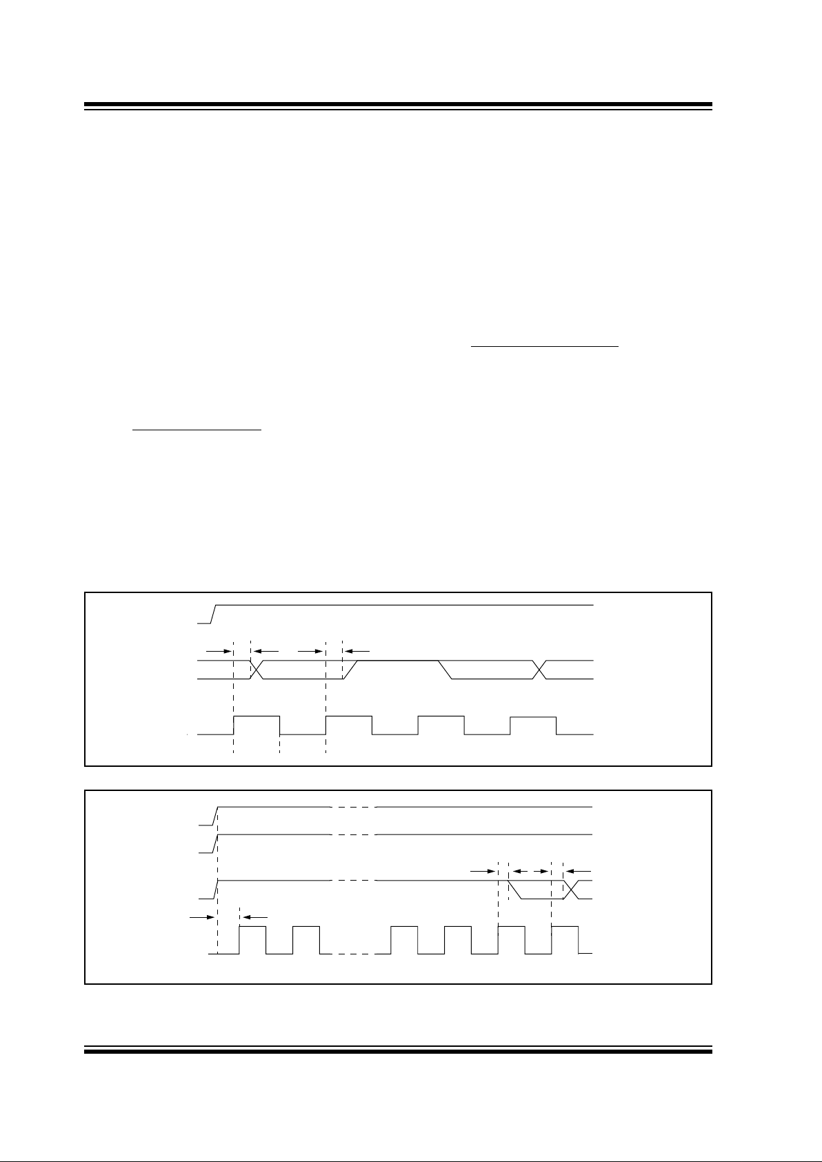
2.1 Transmit-Only Mode
The device will power up in the Transmit-Only Mode at
address 00H. This mode supports a unidirectional
2-wire protocol for continuous transmission of the
contents of the memory array. This device requires that
it be initialized prior to valid data being sent in the Trans-
mit-Only Mode (Section 2.2). In this mode, data is
transmitted on the SDA pin in 8-bit bytes, with each byte
followed by a ninth, null bit (Figure 2-1). The clock
source for the Transmit-Only Mode is provided on the
VCLK pin, and a data bit is output on the rising edge on
this pin. The eight bits in each byte are transmitted most
significant bit first. Each byte within the memory array
will be output in sequence. After address 7Fh in the
memory array is transmitted, the internal address pointers will wrap around to the first memory location (00h)
and continue. The Bi-directional Mode Clock (SCL) pin
must be held high for the device to remain in the
Transmit-Only Mode.
2.2 Initialization Procedure
After VCC has stabilized, the device will be in the
Transmit-Only Mode. Nine clock cycles on the VCLK pin
must be given to the device for it to perform internal
sychronization. During this period, the SDA pin will be
in a high impedance state. On the rising edge of the
tenth clock cycle, the device will output the first valid
data bit which will be the most significant bit in address
00h. (Figure 2-2).
FIGURE 2-1: TRANSMIT-ONLY MODE
FIGURE 2-2: DEVICE INITIALIZATION
SCL
SDA
VCLK
Tvaa Tvaa
Bit 1 (LSB)
Null Bit
Bit 1 (MSB) Bit 7
TvlowTvhigh
Tvaa Tvaa
Bit 8 Bit 7High Impedance for 9 clock cycles
Tvpu
12 891011
SCL
SDA
VCLK
Vcc
1996 Microchip Technology Inc. Preliminary DS21160B-page 5
24LC21A
3.0 BI-DIRECTIONAL MODE
Before the 24LC21A can be switched into the Bi-directional Mode (Figure 3-1), it must enter the transition
mode, which is done by applying a valid high to low
transition on the Bi-directional Mode Clock (SCL). As
soon it enters the transition mode, it looks for a control
byte 1010 000X on the I
2
C bus, and starts to count
pulses on VCLK. Any high to low transition on the SCL
line will reset the count. If it sees a pulse count of 128
on VCLK while the SCL line is idle, it will revert back to
the Transmit-Only Mode, and transmit its contents starting with the most significant bit in address 00h. However, if it detects the control byte on the I
2
C bus,
(Figure 3-2) it will switch to the in the Bi-directional
Mode. Once the device has made the transition to the
Bi-directional mode, the only way to switch the device
back to the Transmit-Only Mode is to remove power
from the device. The mode transition process is shown
in detail in Figure 3-3.
Once the device has switched into the Bi-directional
Mode, the VCLK input is disregarded, with the exception that a logic high level is required to enable write
capability. This mode supports a two-wire Bi-directional
data transmission protocol (I
2
C). In this protocol, a
device that sends data on the bus is defined to be the
transmitter, and a device that receives data from the
bus is defined to be the receiver. The bus must be controlled by a master device that generates the Bi-directional Mode Clock (SCL), controls access to the bus
and generates the START and STOP conditions, while
the 24LC21A acts as the slave. Both master and slave
can operate as transmitter or receiver, but the master
device determines which mode is activated. In the Bidirectional mode, the 24LC21A only responds to
commands for device 1010 000X.
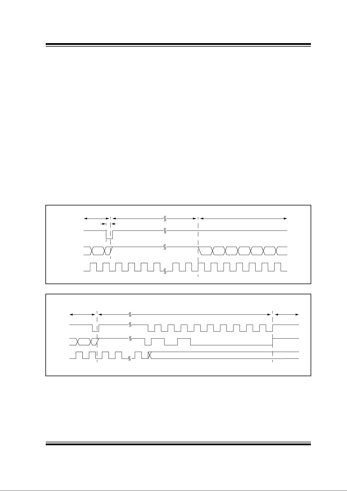
FIGURE 3-1: MODE TRANSITION WITH RECOVERY TO TRANSMIT-ONLY MODE
FIGURE 3-2: SUCCESSFUL MODE TRANSITION TO BI-DIRECTIONAL MODE
TVHZ
SCL
SDA
VCLK
Transmit
Only
MODE
Bi-directional
Recovery to Transmit-Only Mode
Bit8
(MSB of data in 00h)
VCLK count =
1 2 3 4 127 128
Transition Mode with possibility to return to Transmit-Only Mode
Bi-directional
permanently
SCL
SDA
VCLK count = 1 2 n 0
VCLK
Transmit
Only Mode
MODE
S1010 00 0 0 ACK
n < 128
 Loading...