

Microchip Technology Inc 24LC025T-I-ST, 24LC025T-I-SN, 24LC025T-I-P, 24LC025T-ST, 24LC025T-SN Datasheet
...
1997 Microchip Technology Inc.
Preliminary
DS21210A-page 1
M
24LC024/24LC025
FEATURES
• Single supply with operation from 2.5 to 5.5V
• Low power CMOS technology
- 1 mA active current typical
- 10 µ A standby current typical at 5.5V
• Organized as a single block of 128 bytes (256 x 8)
• Hardware write protection for entire array
(24LC024)
• 2-wire serial interface bus, I
2
C compatible
• 100kHz and 400kHz compatibility
• Page-write buffer for up to 16 bytes
• Self-timed write cycle (including auto-erase)
• 3.5 ms typical write cycle time for page write
• Address lines allow up to eight devices on bus
• 10,000,000 erase/write cycles guaranteed
• ESD protection > 4,000V
• Data retention > 200 years
• 8-pin PDIP, SOIC or TSSOP packages
• Available for extended temperature ranges
DESCRIPTION
The Microchip Technology Inc. 24LC024/24LC025 is a
2K bit Serial Electrically Erasable PROM with a voltage
range of 2.5V to 5.5V. The device is organized as a
single block of 256 x 8-bit memory with a 2-wire ser ial
interface. Low current design permits operation with
typical standby and active currents of only 10 µ A and 1
mA respectively. The device has a page-write capability
for up to 16 bytes of data. Functional address lines
allow the connection of up to eight 24LC024/24LC025
devices on the same bus for up to 16K bits of contiguous EEPROM memory. The device is available in the
standard 8-pin PDIP, 8-pin SOIC (150 mil), and TSSOP
packages.
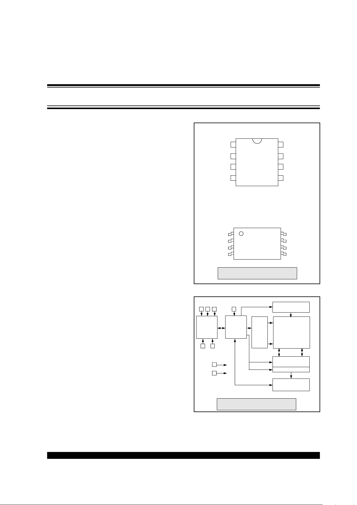
PACKA GE TYPES
BLOCK DIAGRAM
- Commercial (C): 0 ° C to +70 ° C
- Industrial (I): -40 ° C to +85 ° C
PDIP/SOIC
TSSOP
A0
A1
A2
Vss
Vcc
WP*
SCL
SDA
24LC024
25LC025
24LC024
24LC025
1
2
3
4
8
7
6
5
A0
A1
A2
V
SS
VCC
WP*
SCL
SDA
1
2
3
4
8
7
6
5
*WP pin available only on 24LC024. This
pin has no internal connection on 24LC025
I/O
Control
Logic
Memory
Control
Logic
XDEC
HV Generator
EEPROM
Array
Write Protect
Circuitry
YDEC
V
CC
VSS
SENSE AMP
R/W CONTROL
SDA
SCL
A0 A1 A2
WP*
*WP pin available only on 24LC024. This
pin has no internal connection on 24LC025
2K 2.5V I
2
C
™
Serial EEPROM
24LC024/24LC025
DS21210A-page 2
Preliminary
1997 Microchip Technology Inc.
1.0 ELECTRICAL
CHARACTERISTICS
1.1 Maxim
um Ratings*
V
CC
........................................................................7.0V
All inputs and outputs w.r.t. V
SS
......-0.6V to V
CC
+1.0V
Storage temperature...........................-65˚C to +150˚C
Ambient temp. with power applied.......-65˚C to +125˚C
Soldering temperature of leads (10 seconds)...+300˚C
ESD protection on all pins ......................................≥ 4 kV
*Notice: Stresses above those listed under “Maximum ratings” may
cause permanent damage to the device. This is a stress rating only and
functional operation of the device at those or any other conditions
above those indicated in the operational listings of this specification is
not implied. Exposure to maximum rating conditions for extended periods may affect device reliability.
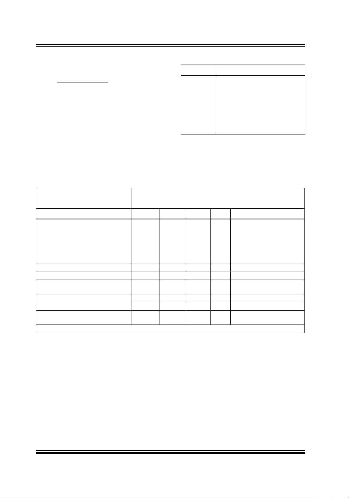
TABLE 1-1: PIN FUNCTION TABLE
Name Function
V
SS
SDA
SCL
V
CC
A0, A1, A2
WP
NC
Ground
Serial Data
Serial Clock
+2.5V to 5.5V Power Supply
Chip Selects
Hardware Write Protect (24LC024)
No internal connection
TABLE 1-2: DC CHARACTERISTICS
All parameters apply across the specified operating ranges unless otherwise
noted.
V
CC
= +2.5V to +5.5V
Commercial (C): Tamb = 0 ° C to +70 ° C
Industrial (I): Tamb = -40 ° C to +85 ° C
Parameter Symbol Min. Max. Units Conditions
SCL and SDA pins:
High level input voltage V
IH
0.7 V
CC
V
Low level input voltage V
IL
0.3 V
CC
V
Hysteresis of Schmitt trigger inputs V
HYS
0.05 V
CC
— V (Note)
Low level output voltage V
OL
0.40 V I
OL
= 3.0 mA, V
CC
= 4.5V
I
OL
= 2.1 mA, V
CC
= 2.5V
Input leakage current I
LI
-10 10
µ
A V
IN
= 0.1V to 5.5V, WP = Vss
Output leakage current I
LO
-10 10
µ
A V
OUT
= 0.1V to 5.5V
Pin capacitance (all inputs/outputs) C
IN
, C
OUT
— 10 pF V
CC
= 5.0V (Note)
Tamb = 25 ° C, f = 1 MHz
Operating current
I
CC
Read — 1 mA V
CC
= 5.5V, SCL = 400 kHz
I
CC
Write — 3 mA V
CC
= 5.5V
Standby current I
CCS
— 50
µ
A V
CC
= 5.5V, SDA = SCL = V
CC
A0, A1, A2 = Vss
Note : This parameter is periodically sampled and not 100% tested.
24LC024/24LC025
1997 Microchip Technology Inc.
Preliminary
DS21210A-page 3
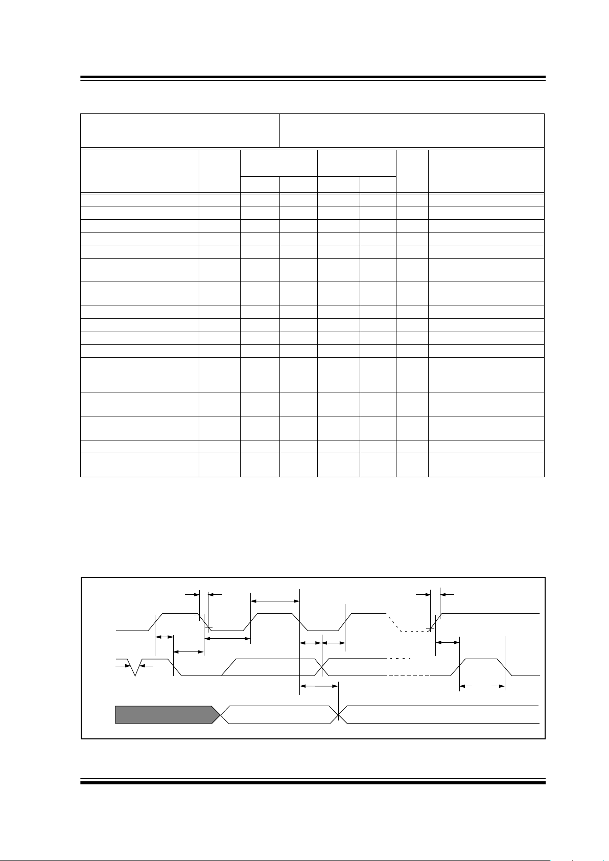
TABLE 1-3: AC CHARACTERISTICS
FIGURE 1-1: BUS TIMING DATA
All parameters apply across the specified operating ranges unless otherwise noted.
Vcc = 2.5V to 5.5V
Commercial (C): Tamb = 0 ° C to +70 ° C
Industrial (I): Tamb = -40 ° C to +85 ° C
Parameter Symbol
Vcc = 2.5V - 5.5V
STD MODE
Vcc = 4.5V - 5.5V
FAST MODE
Units Remarks
Min. Max. Min. Max.
Clock frequency F
CLK
— 100 — 400 kHz
Clock high time T
HIGH
4000 — 600 — ns
Clock low time T
LOW
4700 — 1300 — ns
SDA and SCL rise time T
R
— 1000 — 300 ns (Note 1)
SDA and SCL fall time T
F
— 300 — 300 ns (Note 1)
START condition hold time T
HD
:
STA
4000 — 600 — ns After this period the first
clock pulse is generated
START condition setup time T
SU
:
STA
4700 — 600 — ns Only relevant for repeated
START condition
Data input hold time T
HD
:
DAT
0 — 0 — ns (Note 2)
Data input setup time T
SU
:
DAT
250 — 100 — ns
STOP condition setup time T
SU
:
STO
4000 — 600 — ns
Output valid from clock T
AA
— 3500 — 900 ns (Note 2)
Bus free time T
BUF
4700 — 1300 — ns Time the bus must be free
before a new transmission
can start
Output fall time from V
IH
minimum to V
IL
maximum
T
OF
— 250 20 +0.1
C
B
250 ns (Note 1), C
B
≤
100 pF
Input filter spike suppression
(SDA and SCL pins)
T
SP
— 50 — 50 ns (Note 3)
Write cycle time T
WC
— 10 — 10 ms Byte or Page mode
Endurance 10M — 10M — cycles 25 ° C, V
CC
= 5.0V, Block
Mode (Note 4)
Note 1: Not 100% tested. C
B
= total capacitance of one bus line in pF.
2:
As a transmitter, the device must provide an internal minimum delay time to bridge the undefined region
(minimum 300 ns) of the falling edge of SCL to avoid unintended generation of START or STOP conditions.
3:
The combined T
SP
and V
HYS
specifications are due to Schmitt trigger inputs which provide improved noise
spike suppression. This eliminates the need for a TI specification for standard operation.
4:
This parameter is not tested but guaranteed by characterization. For endurance estimates in a specific
application, please consult the Total Endurance Model which can be obtained on our BBS or website.
SCL
SDA
IN
TSU:STA
SDA
OUT
THD:STA
TLOW
THIGH
TR
TBUF
TAA
THD:DAT TSU:DAT TSU:STO
TSP
TF
24LC024/24LC025
DS21210A-page 4 Preliminary 1997 Microchip Technology Inc.
2.0 PIN DESCRIPTIONS
2.1 SDA Serial Data
This is a bi-directional pin used to transfer addresses
and data into and data out of the device. It is an open
drain terminal, therefore the SDA bus requires a pull-up
resistor to V
CC (typical 10 kΩ for 100 kHz, 2 kΩ for
400 kHz).
For normal data transfer SD A is allow ed to change only
during SCL low. Changes during SCL high are reserved
for indicating the START and STOP conditions.
2.2 SCL Serial Clock
This input is used to synchronize the data transfer from
and to the device.
2.3 A0, A1, A2
The levels on these inputs are compared with the corresponding bits in the slave address. The chip is
selected if the compare is true.
Up to eight 24LC024/24LC025 devices may be connected to the same bus by using different chip select bit
combinations. These inputs must be connected to
either V
CC or VSS.
2.4 WP (24LC024 only)
This is the hardware write protect pin. It must be tied to
V
CC or VSS. If tied to Vcc, the hardware write protection
is enabled. If the WP pin is tied to Vss the hardware
write protection is disabled. Note that the WP pin is
available only on the 24LC024. This pin is not internally
connected on the 24LC025.
2.5 Noise Protection
The 24LC024/24LC025 employs a VCC threshold
detector circuit which disables the internal erase/write
logic if the V
CC is below 1.5 volts at nominal conditions.
The SCL and SDA inputs hav e Schmitt trigger and filter
circuits which suppress noise spikes to assure proper
device operation even on a noisy bus.
3.0 FUNCTIONAL DESCRIPTION
The 24LC024/24LC025 supports a bi-directional 2-wire
bus and data transmission protocol. A device that
sends data onto the bus is defined as transmitter, and
a device receiving data as receiver. The bus has to be
controlled by a master device which generates the
serial clock (SCL), controls the bus access, and generates the START and STOP conditions, while the
24LC024/24LC025 works as slave. Both master and
slave can operate as transmitter or receiver but the
master device determines which mode is activated.
 Loading...