

Microchip Technology Inc 24LC00-I-P, 24LC00-ST, 24LC00-SN, 24LC00-P, 24LC00-OT Datasheet
...
M
128 Bit I
24AA00/24LC00/24C00
2
C™ Bus Serial EEPROM
DEVICE SELECTION TABLE
Device V
24AA00 1.8 - 6.0 C,I
24LC00 2.5 - 6.0 C,I
24C00 4.5 - 5.5 C,I,E
CC
Range Temp Range
FEATURES
• Low power CMOS technology
- 500 µ A typical active current
- 500 nA typical standby current
• Organized as 16 bytes x 8 bits
• 2-wire serial interface bus, I
• 100kHz (1.8V) and 400kHz (5V) compatibility
• Self-timed write cycle (including auto-erase)
• 4 ms maximum byte write cycle time
• 1,000,000 erase/write cycles guaranteed
• ESD protection > 4kV
• Data retention > 200 years
• 8L DIP, SOIC, TSSOP and 5L SOT-23 packages
• Temperature ranges available:
- Commercial (C): 0 ° C to +70 ° C
- Industrial (I): -40 ° C to +85 ° C
- Automotive (E) -40 ° C to +125 ° C
2
C™ compatible
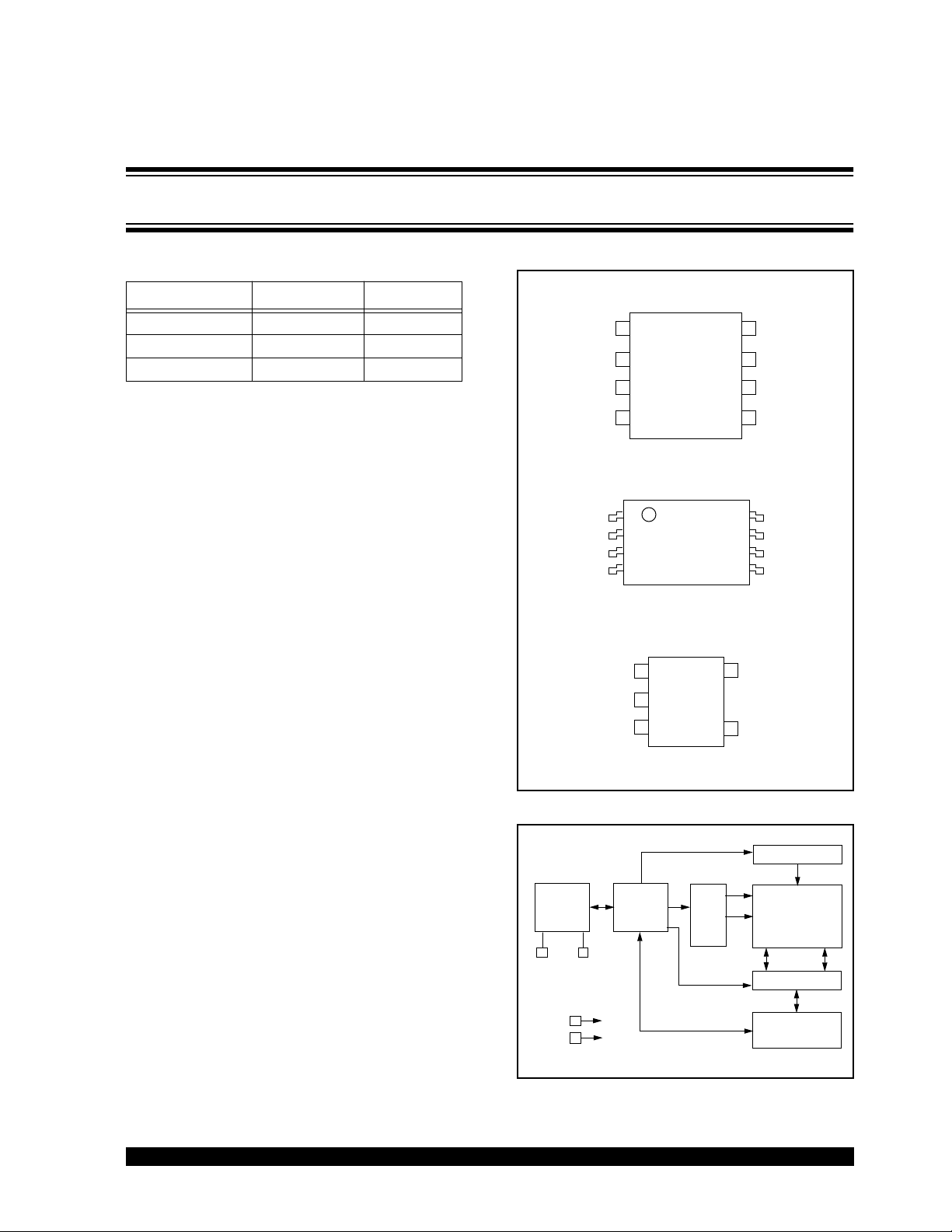
PACKA GE TYPES
8-PIN PDIP/SOIC
SCL
VSS
SDA
1
2
3
4
1
2
3
4
1
2
3
NC
NC
NC
VSS
8-PIN TSSOP
NC
NC
NC
Vss
5-PIN SOT-23
24xx00
24xx00
5
24xx00
4
8
7
6
5
8
7
6
5
VCC
NC
VCC
NC
SCL
SDA
Vcc
NC
SCL
SDA
DESCRIPTION
The Microchip Technology Inc. 24AA00/24LC00/24C00
(24xx00*) is a 128-bit Electrically Erasable PROM
memory organized as 16 x 8 with a 2-wire serial interface. Low voltage design permits operation down to 1.8
volts for the 24xx00 version, and every version maintains a maximum standby current of only 1 µ A and typical active current of only 500 µ A. This device was
designed where a small amount of EEPROM is needed
for the storage of calibration values, ID numbers or
manufacturing information, etc. The 24xx00 is available
in 8ld PDIP, 8ld SOIC (150 mil), 8ld TSSOP and the 5ld
SOT-23 packages.
*24xx00 is used in this document as a generic part number for the 24AA00/24LC00/24C00 devices.
2
I
C is a trademark of Philips Corporation.
1996 Microchip Technology Inc.
Preliminary
BLOCK DIAGRAM
I/O
CONTROL
LOGIC
SCL
SDA
VCC
VSS
MEMORY
CONTROL
LOGIC
XDEC
HV GENERATOR
EEPROM
ARRAY
YDEC
SENSE AMP
R/W CONTROL
DS21178A-page 1
24xx00
µ
µ
1.0 ELECTRICAL
CHARACTERISTICS
1.1 Maxim
Vcc...................................................................................7.0V
All inputs and outputs w.r.t. Vss.................-0.6V to Vcc +1.0V
Storage temperature.....................................-65˚C to +150˚C
Ambient temp. with power applied................. -65˚C to +125˚C
Soldering temperature of leads (10 seconds).............+300˚C
ESD protection on all pins................................................4 kV
*Notice: Stresses above those listed under “Maximum ratings” may
cause permanent damage to the device. This is a stress rating only and
functional operation of the device at those or any other conditions
above those indicated in the operational listings of this specification is
not implied. Exposure to maximum rating conditions for extended periods may affect device reliability.
um Ratings*
TABLE 1-1 PIN FUNCTION TABLE
Name Function
V
SDA
SCL
V
NC
TABLE 1-2 DC CHARACTERISTICS
All Parameters apply across the recommended operating ranges unless otherwise noted
Parameter Symbol Min. Max. Units Conditions
SCL and SDA pins:
High level input voltage V
Low level input voltage V
Hysteresis of Schmitt trigger inputs V
Low level output voltage V
Input leakage current I
Output leakage current I
Pin capacitance (all inputs/outputs) C
Operating current I
Standby current I
Note: This parameter is periodically sampled and not 100% tested.
Commercial (C): Tamb = 0˚C to +70˚C, Vcc = 1.8V to 6.0V
Industrial (I): Tamb = -40˚C to +85˚C, Vcc = 1.8V to 6.0V
Automotive (E) Tamb = -40˚C to +125˚C, Vcc = 4.5V to 5.5V
IH
IL
HYS
OL
LI
LO
,
IN
C
OUT
Write — 2 mA V
CC
CC
I
Read — 1 mA V
CCS
CC
.7 V
CC
.05 V
-10 10
-10 10
—10pFV
—1
SS
Ground
Serial Data
Serial Clock
CC
+1.8V to 6.0V (24AA00)
+2.5V to 6.0V (24LC00)
+4.5V to 5.5V (24C00)
No Internal Connection
V (Note)
.3 V
CC
V (Note)
— V (Note)
.40 V I
AV
AV
µ
AV
= 3.0 mA, V
OL
= 0.1V to 5.5V
IN
OUT
= 0.1V to 5.5V
= 5.0V (Note)
CC
CC
= Vcc
Tamb = 25˚C, f = 1 MHz
= 5.5V, SCL = 400 kHz
CC
CC
= 5.5V, SCL = 400 kHz
= 5.5V, SDA = SCL = V
CC
MIN
CC
FIGURE 1-1: BUS TIMING DATA
TF
SCL
SDA
IN
SDA
OUT
DS21178A-page 2
TSU:STA
TSP
TLOW
THD:STA
THIGH
THD:DAT TSU:DAT TSU:STO
TAA
TR
Preliminary
TBUF
1996 Microchip Technology Inc.
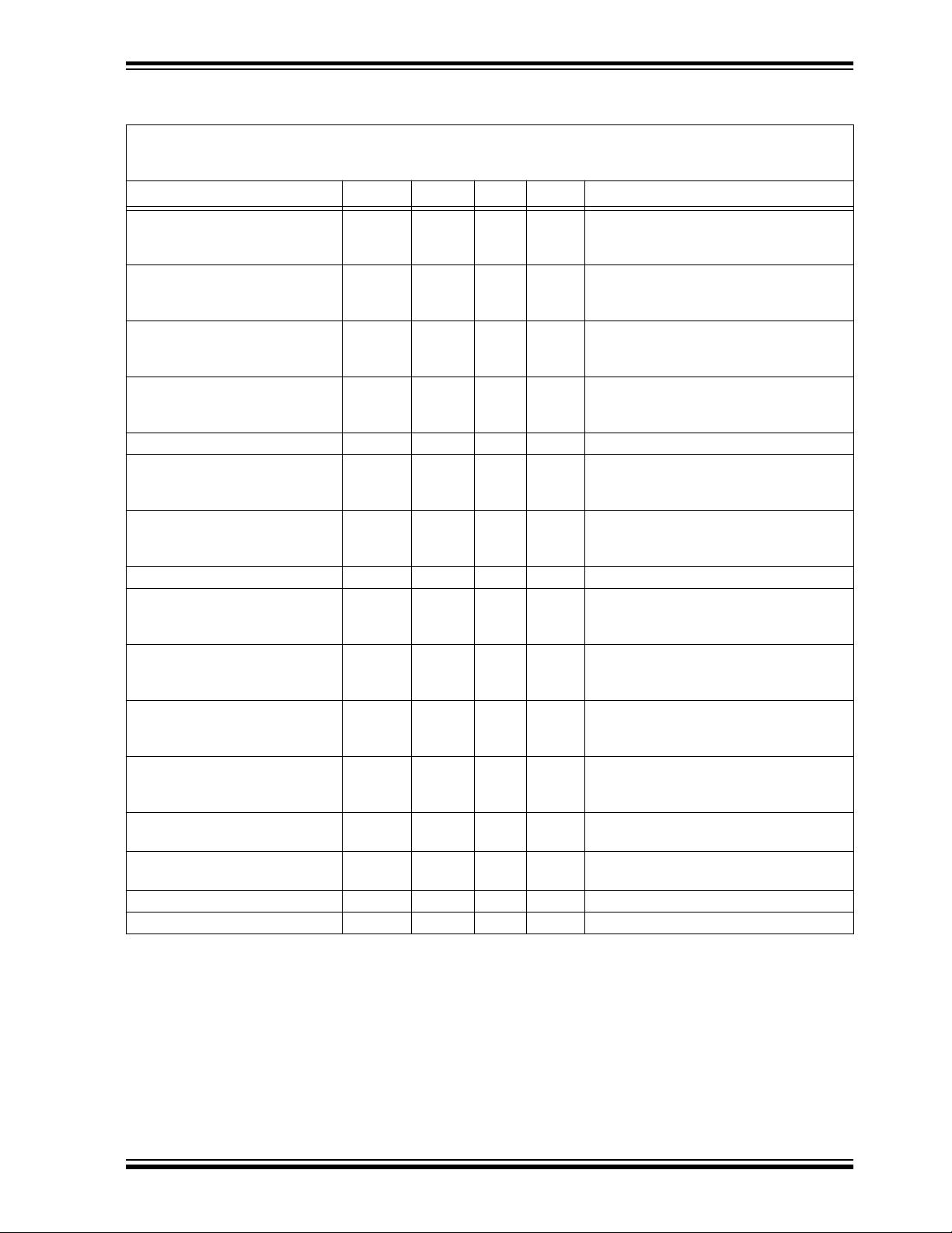
TABLE 1-3 AC CHARACTERISTICS
24xx00
All Parameters apply across all
recommended operating ranges
unless otherwise noted
Commercial (C): Tamb = 0˚C to +70˚C, Vcc = 1.8V to 6.0V
Industrial (I): Tamb = -40˚C to +85˚C, Vcc = 1.8V to 6.0V
Automotive (E): Tamb = -40˚C to +125˚C, Vcc = 4.5V to 5.5V
Parameter Symbol Min Max Units Conditions
Clock frequency F
Clock high time T
Clock low time T
SDA and SCL rise time
CLK
HIGH
LOW
T
R
(Note 1)
SDA and SCL fall time T
START condition hold time T
HD
F
:
STA
START condition setup time TSU:STA 4700
—
—
—
4000
4000
600
4700
4700
1300
—
—
—
100
100
400
—
—
—
—
—
—
1000
1000
300
kHz 4.5V ≤ Vcc ≤ 5.5V (E Temp range)
1.8V ≤ Vcc ≤ 4.5V
4.5V ≤ Vcc ≤ 6.0V
ns 4.5V ≤ Vcc ≤ 5.5V (E Temp range)
1.8V ≤ Vcc ≤ 4.5V
4.5V ≤ Vcc ≤ 6.0V
ns 4.5V ≤ Vcc ≤ 5.5V (E Temp range)
1.8V ≤ Vcc ≤ 4.5V
4.5V ≤ Vcc ≤ 6.0V
ns 4.5V ≤ Vcc ≤ 5.5V (E Temp range)
1.8V ≤ Vcc ≤ 4.5V
4.5V ≤ Vcc ≤ 6.0V
— 300 ns (Note 1)
4000
4000
600
4700
600
—
—
—
—
—
—
ns 4.5V ≤ Vcc ≤ 5.5V (E Temp range)
1.8V ≤ Vcc ≤ 4.5V
4.5V ≤ Vcc ≤ 6.0V
ns 4.5V ≤ Vcc ≤ 5.5V (E Temp range)
1.8V ≤ Vcc ≤ 4.5V
4.5V ≤ Vcc ≤ 6.0V
Data input hold time THD:DAT 0 — ns (Note 2)
Data input setup time T
SU:DAT 250
250
100
STOP condition setup time TSU:STO 4000
4000
600
Output valid from clock
(Note 2)
TAA —
—
—
Bus free time: Time the b us m ust
be free before a new transmission
can start
Output fall time from VIH
minimum to VIL maximum
Input filter spike suppression
TBUF 4700
4700
1300
OF 20+0.1
T
CB
SP — 50 ns (Notes 1, 3)
T
—
—
—
—
—
—
3500
3500
900
—
—
—
ns 4.5V ≤ Vcc ≤ 5.5V (E Temp range)
1.8V ≤ Vcc ≤ 4.5V
4.5V ≤ Vcc ≤ 6.0V
ns 4.5V ≤ Vcc ≤ 5.5V (E Temp range)
1.8V ≤ Vcc ≤ 4.5V
4.5V ≤ Vcc ≤ 6.0V
ns 4.5V ≤ Vcc ≤ 5.5V (E Temp range)
1.8V ≤ Vcc ≤ 4.5V
4.5V ≤ Vcc ≤ 6.0V
ns 4.5V ≤ Vcc ≤ 5.5V (E Temp range)
1.8V ≤ Vcc ≤ 4.5V
4.5V ≤ Vcc ≤ 6.0V
250 ns (Note 1), CB ≤ 100 pF
(SDA and SCL pins)
Write cycle time T
Endurance 1M — cycles 25°C, V
WC —4ms
CC = 5.0V, Block Mode (Note 4)
Note 1: Not 100% tested. CB = total capacitance of one bus line in pF.
2: As a transmitter, the device must provide an internal minimum delay time to bridge the undefined region
(minimum 300 ns) of the falling edge of SCL to avoid unintended generation of START or STOP conditions.
3: The combined T
SP and VHYS specifications are due to new Schmitt trigger inputs which provide improved
noise spike suppression. This eliminates the need for a TI specification for standard operation.
4: This parameter is not tested b ut guaranteed by characterization. For endurance estimates in a specific appli-
cation, please consult the Total Endurance Model which can be obtained on Microchip’s BBS or website.
1996 Microchip Technology Inc.
Preliminary
DS21178A-page 3
24xx00
2.0 PIN DESCRIPTIONS
2.1 SDA Serial Data
This is a bi-directional pin used to transfer addresses
and data into and data out of the device. It is an open
drain terminal, therefore the SDA b us requires a pull-up
resistor to V
kHz).
For normal data transfer SD A is allow ed to change only
during SCL low. Changes during SCL high are reserved
for indicating the START and STOP conditions.
CC (typical 10kΩ for 100 kHz, 1kΩ for 400
2.2 SCL Serial Clock
This input is used to synchronize the data transfer from
and to the device.
2.3 Noise Protection
The SCL and SDA inputs hav e Schmitt trigger and filter
circuits which suppress noise spikes to assure proper
device operation even on a noisy bus.
3.0 FUNCTIONAL DESCRIPTION
The 24xx00 supports a bi-directional 2-wire bus and
data transmission protocol. A device that sends data
onto the bus is defined as a transmitter, and a device
receiving data as a receiver. The bus has to be controlled by a master device which generates the serial
clock (SCL), controls the bus access, and generates
the START and STOP conditions, while the 24xx00
works as slave. Both master and slave can operate as
transmitter or receiver, but the master device determines which mode is activated.
4.0 BUS CHARACTERISTICS
The following bus protocol has been defined:
• Data transfer may be initiated only when the b us is
not busy.
• During data transfer, the data line must remain
stable whenever the clock line is HIGH. Changes
in the data line while the clock line is HIGH will be
interpreted as a START or STOP condition.
Accordingly, the following bus conditions have been
defined (Figure 4-1).
0.1 Stop Data Transfer (C)
A LOW to HIGH transition of the SDA line while the
clock (SCL) is HIGH determines a STOP condition. All
operations must be ended with a STOP condition.
4.3 Data Valid (D)
The state of the data line represents valid data when,
after a START condition, the data line is stable for the
duration of the HIGH period of the clock signal.
The data on the line must be changed during the LOW
period of the clock signal. There is one bit of data per
clock pulse.
Each data transfer is initiated with a START condition
and terminated with a STOP condition. The number of
the data bytes transferred between the START and
STOP conditions is determined by the master device
and is theoretically unlimited.
4.4 Acknowledge
Each receiving device, when addressed, is obliged to
generate an acknowledge after the reception of each
byte. The master device must generate an extra clock
pulse which is associated with this acknowledge bit.
Note: The 24xx00 does not generate any
acknowledge bits if an internal programming cycle is in progress.
The device that acknowledges has to pull down the
SDA line during the acknowledge cloc k pulse in such a
way that the SDA line is stable LOW during the HIGH
period of the acknowledge related clock pulse. Of
course, setup and hold times must be taken into
account. A master must signal an end of data to the
slave by not generating an acknowledge bit on the last
byte that has been clocked out of the sla ve. In this case,
the slave must leave the data line HIGH to enable the
master to generate the STOP condition (Figure 4-2).
4.1 Bus not Busy (A)
Both data and clock lines remain HIGH.
4.2 Start Data Transfer (B)
A HIGH to LOW transition of the SDA line while the
clock (SCL) is HIGH determines a START condition. All
commands must be preceded by a START condition.
DS21178A-page 4 Preliminary 1996 Microchip Technology Inc.
 Loading...