

Page 1

USB2422
2-Port USB 2.0 Hi-Speed Hub Controller
PRODUCT FEATURES
General Description
The Microchip USB2422 hub is a low-power, single
transaction translator, hub controller IC with two
downstream ports for embedded USB solutions. The hub
controller can attach to an upstream port as a Hi-Speed and
Full-Speed hub or as a Full-Speed only hub. The hub
supports Low-Speed, Full-Speed, and Hi-Speed (when
configured as a Hi-Speed hub) downstream devices on the
enabled downstream ports.
All required resistors on the USB ports are integrated into
the hub. This includes all series termination resistors on D+
and D- pins and all required pull-down and pull-up resistors
on D+ and D- pins. The over-current sense inputs for the
downstream facing ports have internal pull-up resistors.
Features
Supports the USB Battery Charging Specification,
Revision 1.1
Fully integrated USB termination and pull-up/pull-
down resistors
Supports a single external 3.3 V supply source;
internal regulators provide 1.2 V internal core voltage
On-chip driver for 24 MHz crystal resonator or
external 24 MHz clock input
ESD protection up to 6 kV on all USB pins
Supports self-powered operation
The hub contains a built-in default configuration; no
external configuration options or components are
required
Downstream ports as non-removable ports
Downstream port power control and over-current
detection on an individual or ganged basis
Supports compound devices on a port-by-port basis
24-pin SQFN (4x4 mm), RoHS-compliant package
Commercial temperature range support:
0ºC to +70ºC
Industrial temperature range support:
-40ºC to +85ºC
Datasheet
Highlights
High performance, low-power, small footprint hub
controller IC with two downstream ports
Fully compliant with the USB 2.0 Specification
Optimized for minimal bill-of-materials and low-cost
designs
Applications
LCD monitors and TVs
Multi-function USB peripherals
PC motherboards
Set-top boxes, DVD players, DVR/PVR
Printers and scanners
PC media drive bay
Portable hub boxes
Mobile PC docking
Embedded systems
Gaming consoles
Cable/DSL modems
HDD enclosures
KVM switches
Server front panels
Point-of-Sale (POS) systems
IP telephony
Automobile/home audio systems
Thin client terminals
2014 Microchip Technology Inc. DS00001726A-page 1
Page 2
ORDER NUMBERS
2-Port USB 2.0 Hi-Speed Hub Controller
Datasheet
Order Numbers:
ROHS COMPLIANT
PACKAGE TEMP. RANGE REEL SIZE
USB2422/MJ
USB2422T/MJ 0ºC to +70ºC
USB2422-I/MJ -40ºC to +85ºC
24-Pin SQFN
4 x 4 mm
0ºC to +70ºC
USB2422T-I/MJ -40ºC to +85ºC
-
4000
-
4000
This product meets the halogen maximum concentration values per IEC61249-2-21
TO OUR VALUED CUSTOMERS
It is our intention to provide our valued customers with the best documentation possible to ensure successful use of your Microchip
products. To this end, we will continue to improve our publications to better suit your needs. Our publications will be refined and
enhanced as new volumes and updates are introduced.
If you have any questions or comments regarding this publication, please contact the Marketing Communications Department via
E-mail at docerrors@microchip.com. We welcome your feedback.
Most Current Data Sheet
To obtain the most up-to-date version of this data sheet, please register at our Worldwide Web site at:
http://www.microchip.com
You can determine the version of a data sheet by examining its literature number found on the bottom outside corner of any page.
The last character of the literature number is the version number, (e.g., DS30000000A is version A of document DS30000000).
Errata
An errata sheet, describing minor operational differences from the data sheet and recommended workarounds, may exist for current devices. As device/documentation issues become known to us, we will publish an errata sheet. The errata will specify the
revision of silicon and revision of document to which it applies.
To determine if an errata sheet exists for a particular device, please check with one of the following:
• Microchip’s Worldwide Web site; http://www.microchip.com
• Your local Microchip sales office (see last page)
When contacting a sales office, please specify which device, revision of silicon and data sheet (include -literature number) you are
using.
Customer Notification System
Register on our web site at www.microchip.com to receive the most current information on all of our products.
DS00001726A-page 2 2014 Microchip Technology Inc.
Page 3

2-Port USB 2.0 Hi-Speed Hub Controller
Datasheet
Conventions
Within this manual, the following abbreviations and symbols are used to improve readability.
Example Description
BIT
FIELD.BIT
x…y Range from x to y, inclusive
BITS[m:n]
PIN Pin Name
zzzzb Binary number (value zzzz)
0xzzz Hexadecimal number (value zzz)
zzh Hexadecimal number (value zz)
rsvd Reserved memory location. Must write 0, read value indeterminate
code Instruction code, or API function or parameter
Section Name Section or Document name
x Don’t care
<Parameter> <> indicate a Parameter is optional or is only used under some conditions
{,Parameter} Braces indicate Parameter(s) that repeat one or more times
[Parameter]
Name of a single bit within a field
Name of a single bit (BIT) in FIELD
Groups of bits from m to n, inclusive
Brackets indicate a nested Parameter. This Parameter is not real and actually decodes
into one or more real parameters.
2014 Microchip Technology Inc. DS00001726A-page 3
Page 4

2-Port USB 2.0 Hi-Speed Hub Controller
Datasheet
Table of Contents
Chapter 1 Block Diagram . . . . . . . . . . . . . . . . . . . . . . . . . . . . . . . . . . . . . . . . . . . . . . . . . . . . . 8
Chapter 2 Pin Descriptions . . . . . . . . . . . . . . . . . . . . . . . . . . . . . . . . . . . . . . . . . . . . . . . . . . . . 9
2.1 Pin Configuration . . . . . . . . . . . . . . . . . . . . . . . . . . . . . . . . . . . . . . . . . . . . . . . . . . . . . . . . . . . . . . . 9
2.2 Pin Table. . . . . . . . . . . . . . . . . . . . . . . . . . . . . . . . . . . . . . . . . . . . . . . . . . . . . . . . . . . . . . . . . . . . . 10
2.3 Pin Descriptions (Grouped by Function). . . . . . . . . . . . . . . . . . . . . . . . . . . . . . . . . . . . . . . . . . . . . 11
2.4 Buffer Type Descriptions . . . . . . . . . . . . . . . . . . . . . . . . . . . . . . . . . . . . . . . . . . . . . . . . . . . . . . . . 14
2.5 Strap Pin Configuration. . . . . . . . . . . . . . . . . . . . . . . . . . . . . . . . . . . . . . . . . . . . . . . . . . . . . . . . . . 14
2.5.1 Non-Removable. . . . . . . . . . . . . . . . . . . . . . . . . . . . . . . . . . . . . . . . . . . . . . . . . . . . . . . . 14
2.5.2 Internal Pull-Down (IPD) . . . . . . . . . . . . . . . . . . . . . . . . . . . . . . . . . . . . . . . . . . . . . . . . . 15
2.5.3 LED . . . . . . . . . . . . . . . . . . . . . . . . . . . . . . . . . . . . . . . . . . . . . . . . . . . . . . . . . . . . . . . . . 15
2.6 Example Applications . . . . . . . . . . . . . . . . . . . . . . . . . . . . . . . . . . . . . . . . . . . . . . . . . . . . . . . . . . . 16
Chapter 3 Battery Charging Support . . . . . . . . . . . . . . . . . . . . . . . . . . . . . . . . . . . . . . . . . . 18
3.1 USB Battery Charging . . . . . . . . . . . . . . . . . . . . . . . . . . . . . . . . . . . . . . . . . . . . . . . . . . . . . . . . . . 18
3.1.1 Special Behavior of PRTPWR Pins . . . . . . . . . . . . . . . . . . . . . . . . . . . . . . . . . . . . . . . . . 18
3.2 Battery Charging Configuration . . . . . . . . . . . . . . . . . . . . . . . . . . . . . . . . . . . . . . . . . . . . . . . . . . . 19
3.2.1 Battery Charging Enabled via SMBus . . . . . . . . . . . . . . . . . . . . . . . . . . . . . . . . . . . . . . . 19
Chapter 4 Configuration Options. . . . . . . . . . . . . . . . . . . . . . . . . . . . . . . . . . . . . . . . . . . . . . 20
4.1 Hub Configuration. . . . . . . . . . . . . . . . . . . . . . . . . . . . . . . . . . . . . . . . . . . . . . . . . . . . . . . . . . . . . . 20
4.2 Resets. . . . . . . . . . . . . . . . . . . . . . . . . . . . . . . . . . . . . . . . . . . . . . . . . . . . . . . . . . . . . . . . . . . . . . . 20
4.2.1 External Hardware RESET_N . . . . . . . . . . . . . . . . . . . . . . . . . . . . . . . . . . . . . . . . . . . . . 20
4.2.2 USB Bus Reset . . . . . . . . . . . . . . . . . . . . . . . . . . . . . . . . . . . . . . . . . . . . . . . . . . . . . . . . 21
4.3 SMBus . . . . . . . . . . . . . . . . . . . . . . . . . . . . . . . . . . . . . . . . . . . . . . . . . . . . . . . . . . . . . . . . . . . . . . 22
4.3.1 SMBus Slave Address. . . . . . . . . . . . . . . . . . . . . . . . . . . . . . . . . . . . . . . . . . . . . . . . . . . 22
4.3.2 Protocol Implementation . . . . . . . . . . . . . . . . . . . . . . . . . . . . . . . . . . . . . . . . . . . . . . . . . 22
4.3.3 Slave Device Timeout . . . . . . . . . . . . . . . . . . . . . . . . . . . . . . . . . . . . . . . . . . . . . . . . . . . 23
4.3.4 Stretching the SCLK Signal . . . . . . . . . . . . . . . . . . . . . . . . . . . . . . . . . . . . . . . . . . . . . . . 23
4.3.5 SMBus Timing . . . . . . . . . . . . . . . . . . . . . . . . . . . . . . . . . . . . . . . . . . . . . . . . . . . . . . . . . 23
4.3.6 Bus Reset Sequence. . . . . . . . . . . . . . . . . . . . . . . . . . . . . . . . . . . . . . . . . . . . . . . . . . . . 23
4.3.7 SMBus Alert Response Address . . . . . . . . . . . . . . . . . . . . . . . . . . . . . . . . . . . . . . . . . . . 23
4.4 SMBus Registers . . . . . . . . . . . . . . . . . . . . . . . . . . . . . . . . . . . . . . . . . . . . . . . . . . . . . . . . . . . . . . 24
4.4.1 Vendor ID Least Significant Bit Register (VIDL) . . . . . . . . . . . . . . . . . . . . . . . . . . . . . . . 25
4.4.2 Vendor ID Most Significant Bit Register (VIDM) . . . . . . . . . . . . . . . . . . . . . . . . . . . . . . . 25
4.4.3 Product ID Least Significant Bit Register (PIDL) . . . . . . . . . . . . . . . . . . . . . . . . . . . . . . . 26
4.4.4 Product ID Most Significant Bit Register (PIDM) . . . . . . . . . . . . . . . . . . . . . . . . . . . . . . . 26
4.4.5 Device ID Least Significant Bit Register (DIDL). . . . . . . . . . . . . . . . . . . . . . . . . . . . . . . . 26
4.4.6 Device ID Most Significant Bit Register (DIDM). . . . . . . . . . . . . . . . . . . . . . . . . . . . . . . . 26
4.4.7 Configuration Data Byte 1 Register (CFG1) . . . . . . . . . . . . . . . . . . . . . . . . . . . . . . . . . . 27
4.4.8 Configuration Data Byte 2 Register (CFG2) . . . . . . . . . . . . . . . . . . . . . . . . . . . . . . . . . . 29
4.4.9 Configuration Data Byte 3 Register (CFG3) . . . . . . . . . . . . . . . . . . . . . . . . . . . . . . . . . . 30
4.4.10 Non-Removable Device Register (NRD) . . . . . . . . . . . . . . . . . . . . . . . . . . . . . . . . . . . . . 30
4.4.11 Port Disable for Self-Powered Operation Register (PDS) . . . . . . . . . . . . . . . . . . . . . . . . 31
4.4.12 Port Disable for Bus-Powered Operation Register (PDB) . . . . . . . . . . . . . . . . . . . . . . . . 31
4.4.13 Max Power for Self-Powered Operation Register (MAXPS) . . . . . . . . . . . . . . . . . . . . . . 32
4.4.14 Max Power for Bus-Powered Operation Register (MAXPB) . . . . . . . . . . . . . . . . . . . . . . 32
4.4.15 Hub Controller Max Current for Self-Powered Operation Register (HCMCS) . . . . . . . . . 32
4.4.16 Hub Controller Max Power for Bus-Powered Operation Register (HCMCB). . . . . . . . . . 33
4.4.17 Power-On Time Register (PWRT) . . . . . . . . . . . . . . . . . . . . . . . . . . . . . . . . . . . . . . . . . . 33
4.4.18 Language ID High Register (LANGIDH) . . . . . . . . . . . . . . . . . . . . . . . . . . . . . . . . . . . . . 33
DS00001726A-page 4 2014 Microchip Technology Inc.
Page 5

2-Port USB 2.0 Hi-Speed Hub Controller
Datasheet
4.4.19 Language ID Low Register (LANGIDL) . . . . . . . . . . . . . . . . . . . . . . . . . . . . . . . . . . . . . . 33
4.4.20 Manufacturer String Length Register (MFRSL) . . . . . . . . . . . . . . . . . . . . . . . . . . . . . . . . 34
4.4.21 Product String Length Register (PRDSL) . . . . . . . . . . . . . . . . . . . . . . . . . . . . . . . . . . . . 34
4.4.22 Serial String Length Register (SERSL) . . . . . . . . . . . . . . . . . . . . . . . . . . . . . . . . . . . . . . 34
4.4.23 Manufacturer String Registers (MANSTR) . . . . . . . . . . . . . . . . . . . . . . . . . . . . . . . . . . . 34
4.4.24 Product String Registers (PRDSTR) . . . . . . . . . . . . . . . . . . . . . . . . . . . . . . . . . . . . . . . . 35
4.4.25 Serial String Registers (SERSTR) . . . . . . . . . . . . . . . . . . . . . . . . . . . . . . . . . . . . . . . . . . 35
4.4.26 Battery Charging Enable Register (BC_EN) . . . . . . . . . . . . . . . . . . . . . . . . . . . . . . . . . . 35
4.4.27 Boost Upstream Register (BOOSTUP) . . . . . . . . . . . . . . . . . . . . . . . . . . . . . . . . . . . . . . 36
4.4.28 Boost Downstream Register (BOOST40) . . . . . . . . . . . . . . . . . . . . . . . . . . . . . . . . . . . . 36
4.4.29 Port Swap Register (PRTSP) . . . . . . . . . . . . . . . . . . . . . . . . . . . . . . . . . . . . . . . . . . . . . 37
4.4.30 Port 1/2 Remap Register (PRTR12) . . . . . . . . . . . . . . . . . . . . . . . . . . . . . . . . . . . . . . . . 38
4.4.31 Status/Command Register (STCD) . . . . . . . . . . . . . . . . . . . . . . . . . . . . . . . . . . . . . . . . . 39
Chapter 5 DC Parameters. . . . . . . . . . . . . . . . . . . . . . . . . . . . . . . . . . . . . . . . . . . . . . . . . . . . 40
5.1 Maximum Guaranteed Ratings . . . . . . . . . . . . . . . . . . . . . . . . . . . . . . . . . . . . . . . . . . . . . . . . . . . . 40
5.2 Operating Conditions . . . . . . . . . . . . . . . . . . . . . . . . . . . . . . . . . . . . . . . . . . . . . . . . . . . . . . . . . . . 40
5.2.1 Pin Capacitance . . . . . . . . . . . . . . . . . . . . . . . . . . . . . . . . . . . . . . . . . . . . . . . . . . . . . . . 43
Chapter 6 AC Specifications . . . . . . . . . . . . . . . . . . . . . . . . . . . . . . . . . . . . . . . . . . . . . . . . . . 44
6.1 Oscillator/Crystal. . . . . . . . . . . . . . . . . . . . . . . . . . . . . . . . . . . . . . . . . . . . . . . . . . . . . . . . . . . . . . . 44
6.2 External Clock. . . . . . . . . . . . . . . . . . . . . . . . . . . . . . . . . . . . . . . . . . . . . . . . . . . . . . . . . . . . . . . . . 45
6.2.1 USB 2.0 . . . . . . . . . . . . . . . . . . . . . . . . . . . . . . . . . . . . . . . . . . . . . . . . . . . . . . . . . . . . . . 45
6.3 SMBus Interface . . . . . . . . . . . . . . . . . . . . . . . . . . . . . . . . . . . . . . . . . . . . . . . . . . . . . . . . . . . . . . . 45
Chapter 7 Package Outline . . . . . . . . . . . . . . . . . . . . . . . . . . . . . . . . . . . . . . . . . . . . . . . . . . . 46
Chapter 8 Datasheet Revision History . . . . . . . . . . . . . . . . . . . . . . . . . . . . . . . . . . . . . . . . . . 49
2014 Microchip Technology Inc. DS00001726A-page 5
Page 6

2-Port USB 2.0 Hi-Speed Hub Controller
Datasheet
List of Figures
Figure 1.1 USB2422 Block Diagram . . . . . . . . . . . . . . . . . . . . . . . . . . . . . . . . . . . . . . . . . . . . . . . . . . . . . 8
Figure 2.1 USB2422 24-Pin SQFN . . . . . . . . . . . . . . . . . . . . . . . . . . . . . . . . . . . . . . . . . . . . . . . . . . . . . . 9
Figure 2.2 Non-Removable Pin Strap Example . . . . . . . . . . . . . . . . . . . . . . . . . . . . . . . . . . . . . . . . . . . 14
Figure 2.3 IPD Pin Strap Example . . . . . . . . . . . . . . . . . . . . . . . . . . . . . . . . . . . . . . . . . . . . . . . . . . . . . 15
Figure 2.4 LED Pin Strap Example . . . . . . . . . . . . . . . . . . . . . . . . . . . . . . . . . . . . . . . . . . . . . . . . . . . . . 15
Figure 2.5 Example Application - SoC Based Design . . . . . . . . . . . . . . . . . . . . . . . . . . . . . . . . . . . . . . . 16
Figure 2.6 Example Application - Non-SoC Based Design . . . . . . . . . . . . . . . . . . . . . . . . . . . . . . . . . . . 16
Figure 3.1 Battery Charging via External Power Supply . . . . . . . . . . . . . . . . . . . . . . . . . . . . . . . . . . . . . 18
Figure 4.1 Hub Configuration Timing . . . . . . . . . . . . . . . . . . . . . . . . . . . . . . . . . . . . . . . . . . . . . . . . . . . 21
Figure 4.2 Block Write . . . . . . . . . . . . . . . . . . . . . . . . . . . . . . . . . . . . . . . . . . . . . . . . . . . . . . . . . . . . . . . 22
Figure 4.3 Block Read. . . . . . . . . . . . . . . . . . . . . . . . . . . . . . . . . . . . . . . . . . . . . . . . . . . . . . . . . . . . . . . 23
Figure 5.1 Supply Rise Time Model . . . . . . . . . . . . . . . . . . . . . . . . . . . . . . . . . . . . . . . . . . . . . . . . . . . . 41
Figure 6.1 Typical Crystal Circuit . . . . . . . . . . . . . . . . . . . . . . . . . . . . . . . . . . . . . . . . . . . . . . . . . . . . . . 44
Figure 6.2 Formula to Find the Value of C1 and C2 . . . . . . . . . . . . . . . . . . . . . . . . . . . . . . . . . . . . . . . . 44
Figure 7.1 24-SQFN Package . . . . . . . . . . . . . . . . . . . . . . . . . . . . . . . . . . . . . . . . . . . . . . . . . . . . . . . . . 46
Figure 7.2 Taping Dimensions and Part Orientation . . . . . . . . . . . . . . . . . . . . . . . . . . . . . . . . . . . . . . . . 47
Figure 7.3 Reel Dimensions . . . . . . . . . . . . . . . . . . . . . . . . . . . . . . . . . . . . . . . . . . . . . . . . . . . . . . . . . . 48
Figure 7.4 Tape Length and Part Quantity . . . . . . . . . . . . . . . . . . . . . . . . . . . . . . . . . . . . . . . . . . . . . . . 48
DS00001726A-page 6 2014 Microchip Technology Inc.
Page 7

2-Port USB 2.0 Hi-Speed Hub Controller
Datasheet
List of Tables
Table 2.1 USB2422 Pin Table . . . . . . . . . . . . . . . . . . . . . . . . . . . . . . . . . . . . . . . . . . . . . . . . . . . . . . . . . 10
Table 2.2 USB2422 Pin Descriptions . . . . . . . . . . . . . . . . . . . . . . . . . . . . . . . . . . . . . . . . . . . . . . . . . . . 11
Table 2.3 Buffer Type Descriptions . . . . . . . . . . . . . . . . . . . . . . . . . . . . . . . . . . . . . . . . . . . . . . . . . . . . . 14
Table 2.4 Strap Option Summary . . . . . . . . . . . . . . . . . . . . . . . . . . . . . . . . . . . . . . . . . . . . . . . . . . . . . . 14
Table 2.5 Example Applications - Resistor/Capacitor Values . . . . . . . . . . . . . . . . . . . . . . . . . . . . . . . . . 17
Table 4.1 Hub Configuration Options . . . . . . . . . . . . . . . . . . . . . . . . . . . . . . . . . . . . . . . . . . . . . . . . . . . 20
Table 4.2 Hub Configuration Timing . . . . . . . . . . . . . . . . . . . . . . . . . . . . . . . . . . . . . . . . . . . . . . . . . . . . 21
Table 5.1 DC Electrical Characteristics . . . . . . . . . . . . . . . . . . . . . . . . . . . . . . . . . . . . . . . . . . . . . . . . . . 41
Table 5.2 Pin Capacitance. . . . . . . . . . . . . . . . . . . . . . . . . . . . . . . . . . . . . . . . . . . . . . . . . . . . . . . . . . . . 43
Table 6.1 Crystal Circuit Legend . . . . . . . . . . . . . . . . . . . . . . . . . . . . . . . . . . . . . . . . . . . . . . . . . . . . . . . 44
Table 8.1 Revision History. . . . . . . . . . . . . . . . . . . . . . . . . . . . . . . . . . . . . . . . . . . . . . . . . . . . . . . . . . . . 49
2014 Microchip Technology Inc. DS00001726A-page 7
Page 8
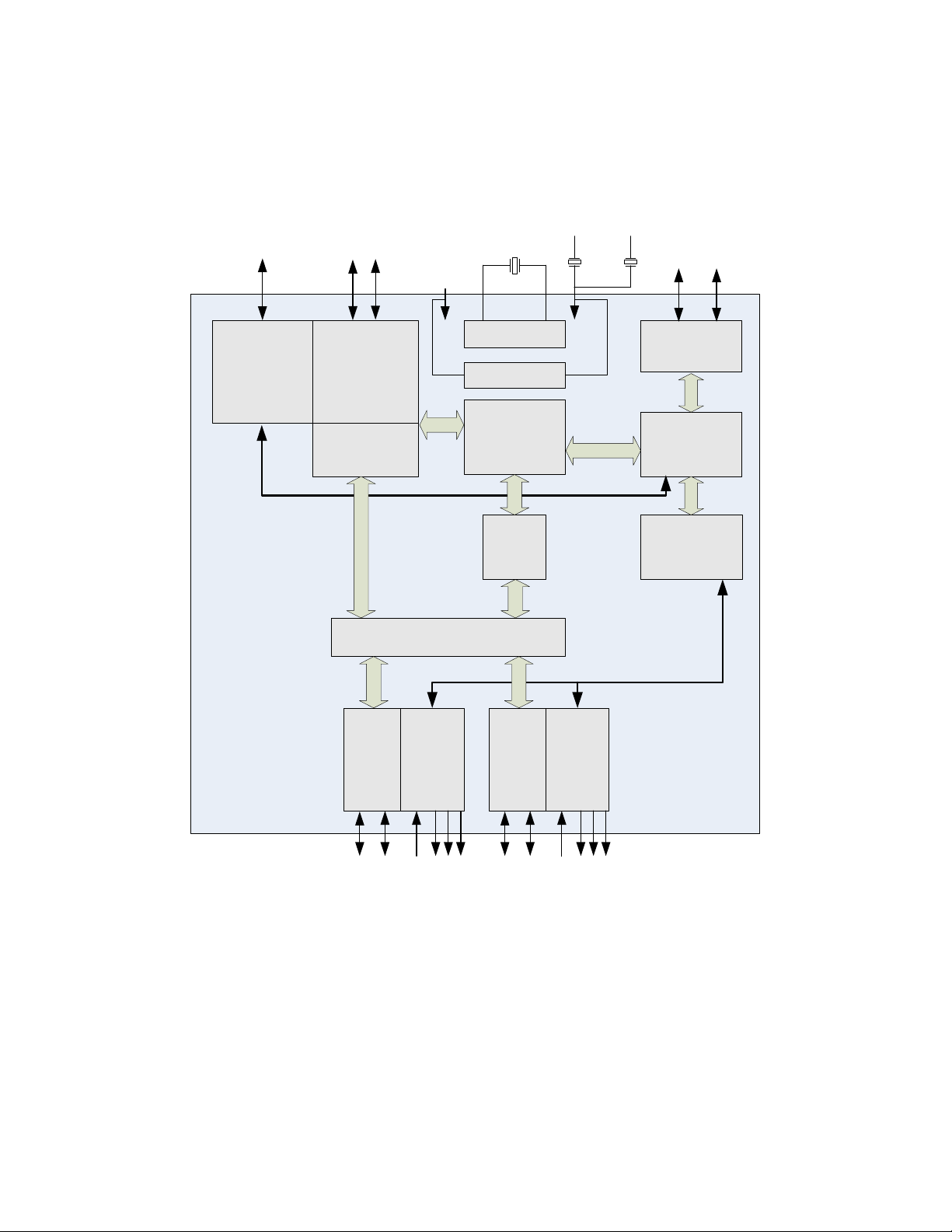
Chapter 1 Block Diagram
To Upstream
V
BUS
3.3V
Upstream
PHY
Upstream USB
Data
Repeater
Controller
SIE
Serial
Interface
PLL
24 MHz Crystal
To
SMBus Master
Routing & Port Re-Ordering
Logic
SMBCLK
SMBDATA
Port
Controller
Bus-Power
Detect/V
BUS
Pulse
TT
PHY#1
Port #1
OC
Sense
Switch
Driver
PHY#2
Port #2
OC
Sense
Switch
Driver
USB Data
Downstream
OC Sense
Switch
USB Data
Downstream
OC Sense
Switch
CRFILT PLLFILT
1.2V Reg
2-Port USB 2.0 Hi-Speed Hub Controller
Datasheet
Figure 1.1 USB2422 Block Diagram
DS00001726A-page 8 2014 Microchip Technology Inc.
Page 9
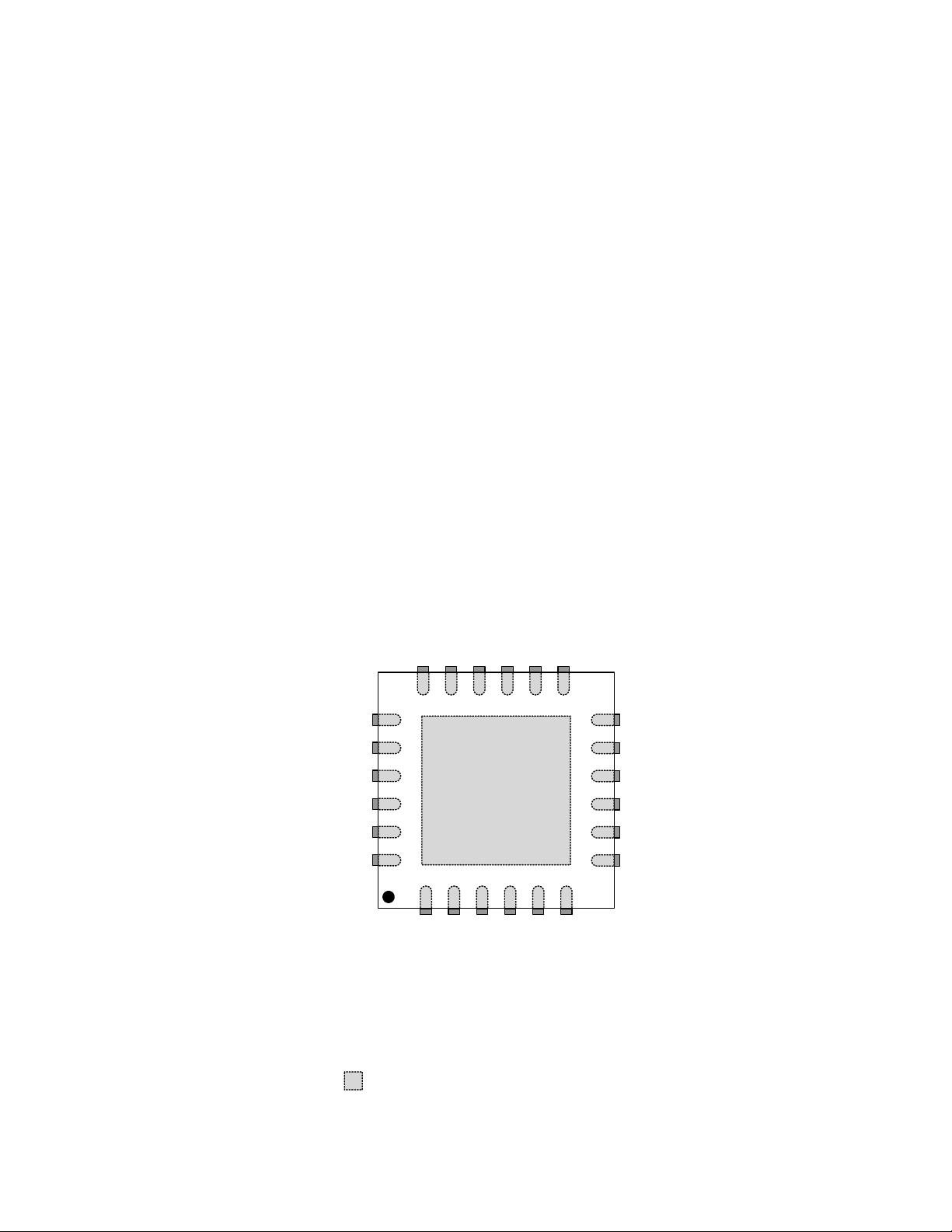
2-Port USB 2.0 Hi-Speed Hub Controller
Thermal Slug
(must be connected to VSS)
12
11
10
9
8
7
USBDP_UP
19
XTALOUT/(CLKIN_EN)
20
XTALIN/CLKIN
21
RBIAS
24
23
PLLFILT
22
1
VDD33
2
USBDP_DN1/PRT_DIS_P1
3
USBDM_DN2/PRT_DIS_M2
4
USBDP_DN2/PRT_DIS_P2
5
6
USBDM_DN1/PRT_DIS_M1
NC
USBDM_UP
17
SUSP_IND/LOCAL_PWR/(NON_REM0)16VBUS_DET
RESET_N
15
14
SMBCLK/CFG_SEL0
VDD33
18
13
SMBDATA/NON_REM1
Indicates pins on the bottom of the device.
OCS1_N
PRTPWR1/(BC_EN1)
VDD33
CRFILT
PRTPWR2
OCS2_N
USB2422
(Top View SQFN-24)
Datasheet
Chapter 2 Pin Descriptions
This chapter is organized by a set of pin configurations followed by a corresponding pin list organized
by function according to their associated interface. A detailed description list of each signal (named in
the pin list) is organized by function in Table 2.2, “USB2422 Pin Descriptions,” on page 11. Refer to
Table 2.3, “Buffer Type Descriptions,” on page 14 for a list of buffer types.
An N at the end of a signal name indicates that the active (asserted) state occurs when the signal is
at a low voltage level. When the N is not present, the signal is asserted when it is at a high voltage
level. The terms assertion and negation are used exclusively in order to avoid confusion when working
with a mixture of active low and active high signals. The term assert, or assertion, indicates that a
signal is active, independent of whether that level is represented by a high or low voltage. The term
negate, or negation, indicates that a signal is inactive.
2.1 Pin Configuration
2014 Microchip Technology Inc. DS00001726A-page 9
Figure 2.1 USB2422 24-Pin SQFN
Page 10

2.2 Pin Table
2-Port USB 2.0 Hi-Speed Hub Controller
Datasheet
Table 2.1 USB2422 Pin Table
UPSTREAM USB 2.0 INTERFACES (3 PINS)
USBDM_UP
USBDP_DN1/
PRT_DIS_P1
PRTPWR1/
BC_EN1
RBIAS
SMBDATA/
NON_REM1
XTALIN/
CLKIN
NC
USBDM_UP
DOWNSTREAM 2-PORT USB 2.0 INTERFACES (9 PINS)
USBDM_DN1/
PRT_DIS_M1
PRTPWR2 OCS1_N OCS2_N
SERIAL PORT INTERFACE (2 PINS)
SMBCLK/
CFG_SEL
MISC (5 PINS)
XTALOUT/
CLKIN_EN
VBUS_DET
USBDP_DN2/
PRT_DIS_P2
RESET_N
USBDM_DN2/
PRT_DIS_M2
SUSP_IND/
LOCAL_PWR/
NON_REM0
POWER, GROUND, AND NO CONNECTS (5 PINS)
(3) VDD33 CRFILT PLLFILT VSS
TOTAL 24
DS00001726A-page 10 2014 Microchip Technology Inc.
Page 11

2-Port USB 2.0 Hi-Speed Hub Controller
Datasheet
2.3 Pin Descriptions (Grouped by Function)
Table 2.2 USB2422 Pin Descriptions
PIN
# SYMBOL
19
20
16 VBUS_DET I Detect Upstream VBUS Power:
5
3
and
4
2
USBDM_UP
USBDP_UP
USBDP_DN[2:1]/
PRT_DIS_P[2:1]
and
USBDN_DN[2:1]/
PRT_DIS_M[2:1]
BUFFER
TYPE DESCRIPTION
UPSTREAM USB 2.0 INTERFACES
IO-U USB Bus Data:
Connect to the upstream USB bus data signals (host, port, or
upstream hub).
Detects the state of upstream VBUS power. The hub monitors
VBUS_DET to determine when to assert the internal D+ pull-up
resistor (signalling a connect event)
When designing a detachable hub, this pin should be connected to
VBUS on the upstream port via a 2:1 voltage divider. Two 100 kΩ
resistors are suggested.
For self-powered applications with a permanently attached host, this
pin must be connected to a dedicated host control output, or
connected to the 3.3 V domain that powers the host (typically VDD33).
DOWNSTREAM USB 2.0 INTERFACES
IO-U Hi-Speed USB Data:
Connect to the downstream USB peripheral devices attached to the
hub’s ports.
Port Disable Strap Option:
If this strap is enabled by package and configuration settings (see
Table 4.1, "Hub Configuration Options"), this pin will be sampled at
RESET_N negation to determine if the port is disabled.
Both USB data pins for the corresponding port must be tied to VDD33
to disable the associated downstream port.
7 PRTPWR1/ O12 USB Power Enable:
Enables power to USB peripheral devices that are downstream, where
the hub supports active high power controllers only.
BC_EN1 IPD Battery Charging Strap Option:
Port 1 pin will be sampled at RESET_N negation to determine if port
1 supports the battery charging protocol (and thus the supporting
external port power controllers) that would enable a device to draw the
currents per the USB Battery Charging Specification.
This pin has an internal pull-down that will be removed after the strap
option hold time is completed.
BC_EN1= 1: Battery charging feature is supported for port 1
BC_EN1= 0: Battery charging feature is not supported for port 1
11 PRTPWR2 O12 USB Power Enable:
Enables power to USB peripheral devices that are downstream, where
the hub supports active high power controllers only.
8
12
2014 Microchip Technology Inc. DS00001726A-page 11
OCS1_N
OCS2_N
IPU Over-Current Sense:
Input from external current monitor indicating an over-current
condition. This pin contains an internal pull-up to the 3.3 V supply.
Page 12

2-Port USB 2.0 Hi-Speed Hub Controller
Table 2.2 USB2422 Pin Descriptions (continued)
Datasheet
PIN
# SYMBOL
BUFFER
TYPE DESCRIPTION
24 RBIAS I-R USB Transceiver Bias:
A12.0 kΩ (+/- 1%) resistor is attached from ground to this pin to set
the transceiver’s internal bias settings.
SERIAL PORT INTERFACE
13 SMBDATA I/OSD12 System Management Bus Data
NON_REM1 Non-removable Port Strap Option:
This pin is sampled (in conjunction with SUSP_IND/NON_REM0) at
RESET_N negation to determine if ports [2:1] contain permanently
attached (non-removable) devices:
NON_REM[1:0] = 00: all ports are removable
NON_REM[1:0] = 01: port 1 is non-removable
NON_REM[1:0] = 10: ports 1 and 2 are non-removable
NON_REM[1:0] = 11: reserved
See Section 2.5, "Strap Pin Configuration" for details.
14 SMBCLK/ I/OSD12 System Management Bus Clock
CFG_SEL Configuration Select:
The logic state of this multifunction pin is internally latched on the
rising edge of RESET_N (RESET_N negation), and will determine the
hub configuration method as described in Table 4.1.
MISC
22 XTALIN/
CLKIN
ICLKx 24 MHz Crystal or External Clock Input:
This pin connects to either one terminal of the crystal or to an external
24 MHz clock when a crystal is not used.
21 XTALOUT OCLKx Crystal Output:
This is the other terminal of the crystal circuit with 1.2 V p-p output and
a weak (< 1 mA) driving strength. When an external clock source is
used to drive XTALIN/CLKIN, leave this pin unconnected, or use with
appropriate caution.
15 RESET_N IS RESET Input:
The system must reset the chip by driving this input low. The minimum
active low pulse is 1 μs.
6 NC IPD Treat as a no connect pin or connect to ground. No trace or signal
should be routed or attached to this pin.
DS00001726A-page 12 2014 Microchip Technology Inc.
Page 13

2-Port USB 2.0 Hi-Speed Hub Controller
Datasheet
Table 2.2 USB2422 Pin Descriptions (continued)
PIN
# SYMBOL
BUFFER
TYPE DESCRIPTION
17 SUSP_IND I/O12 Suspend Indicator:
Indicates the USB state of the hub.
negated : unconfigured, or configured and in USB Suspend
asserted : Hub is configured, and is active (i.e., not in suspend)
LOCAL_PWR Local Power:
This input selects whether the hub reports itself as bus or self-powered
when dynamic power switching is enabled via the Dynamic Power
Enable (DYNAMIC) bit of the Configuration Data Byte 2 Register
(CFG2). This pin is sampled at POR/Reset before the USB Hub Attach
command is sent. Once the hub has entered the attach state (as
indicated by the USB Attach and Write Protect (USB_ATTACH) bit of
the Status/Command Register (STCD)), this pin cannot be changed.
Low : self/local power source is not available (i.e., the Hub gets all
power from the upstream USB VBus).
High : self/local power source is available.
Note: Never tie this pin directly to VDD33, as doing so may cause
it to act as SUSP_IND.
Note: This pin assumes the meaning of local power input only if
properly configured via SMBus. If the hub is configured via
straps, it is NON_REM0 at reset and SUSP_IND after reset.
(NON_REM0) Non-Removable Port Strap Option:
This pin is sampled (in conjunction with SUSP_IND/NON_REM0) at
RESET_N negation to determine if ports [2:1] contain permanently
attached (non-removable) devices:
NON_REM[1:0] = 00: all ports are removable
NON_REM[1:0] = 01: port 1 is non-removable
NON_REM[1:0] = 10: ports 1 and 2 are non-removable
NON_REM[1:0] = 11: reserved
See Section 2.5, "Strap Pin Configuration" for details.
POWER, GROUND, and NO CONNECTS
1
9
18
VDD33 3.3 V power to the chip.
A 1.0 μF low-ESR capacitor to VSS is required on pin 9 as close as
possible to the pin. A 0.1 μF low-ESR capacitor to VSS is required on
pin 1 as close as possible to the pin.
10 CRFILT VDD Core Regulator Filter Capacitor:
This pin requires a 1.0 μF low-ESR capacitor to VSS for proper
operation.
23 PLLFILT PLL Regulator Filter Capacitor:
This pin can have up to a 0.1 μF low-ESR capacitor to VSS, or be left
unconnected.
VSS Ground Pad/ePad:
The package slug is the only VSS for the device and must be tied to
ground with multiple vias.
2014 Microchip Technology Inc. DS00001726A-page 13
Page 14
2.4 Buffer Type Descriptions
HUB
I/O Strap Pin Strap High
+V
HUB
I/O Strap Pin Strap Low
GND
R kΩ
R kΩ
Table 2.3 Buffer Type Descriptions
BUFFER DESCRIPTION
I/O Input/Output
IPD Input with internal weak pull-down resistor
IPU Input with internal weak pull-up resistor
IS Input with Schmitt trigger
I/O12 Input/Output buffer with 12 mA sink and 12 mA source
ICLKx XTAL clock input
OCLKx XTAL clock output
I-R RBIAS
I/O-U Analog Input/Output defined in USB specification
2-Port USB 2.0 Hi-Speed Hub Controller
Datasheet
2.5 Strap Pin Configuration
If a pin's strap function is enabled through hub configuration selection (Ta b le 4 .1 ), the strap pins must
be pulled either high or low using the values provided in Ta bl e 2. 4 . Each strap option is dependent on
the pin’s buffer type, as outlined in the sections that follow.
Table 2.4 Strap Option Summary
STRAP OPTION RESISTOR VALUE BUFFER TYPE NOTES
Non-Removable 47 - 100 kΩ I/O
Internal Pull-Down
(IPD)
10 kΩ IPD
LED 47 - 100 kΩ I/O
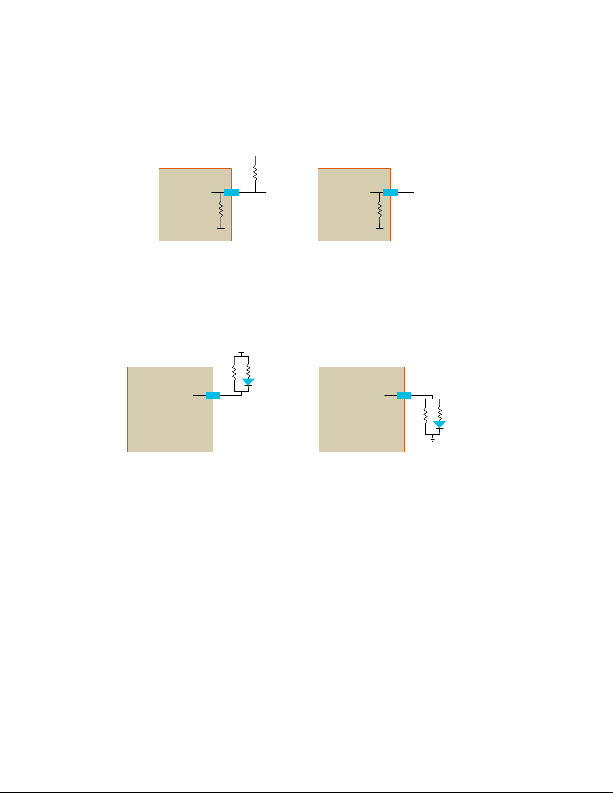
2.5.1 Non-Removable
If a strap pin’s buffer type is I/O, an external pull-up or pull-down must be implemented as shown in
Figure 2.2. Use Strap High to set the strap option to 1 and Strap Low to set the strap option to 0. When
implementing the Strap Low option, no additional components are needed (i.e., the internal pull-down
provides the resistor)
Only applicable to port power pins
Contains a built-in resistor
DS00001726A-page 14 2014 Microchip Technology Inc.
Figure 2.2 Non-Removable Pin Strap Example
Page 15
2-Port USB 2.0 Hi-Speed Hub Controller
HUBHUB
IPD Strap Pin Strap High
R kΩ
+V
VSS
IPD Strap Pin Strap Low
VSS
HUB
Strap Pin
LED/
Strap High
HUB
Strap Pin
LED/
Strap Low
R
kΩ
R
kΩ
Datasheet
2.5.2 Internal Pull-Down (IPD)
If a strap pin’s buffer type is IPD, one of the two hardware configurations outlined in Figure 2.3 must
be implemented. Use the Strap High configuration to set the strap option value to 1 and Strap Low to
set the strap option value to 0.
Figure 2.3 IPD Pin Strap Example
2.5.3 LED
If a strap pin’s buffer type is I/O and shares functionality with an LED, the hardware configuration
outlined below must be implemented. The internal logic will drive the LED appropriately (active high or
low) depending on the sampled strap option. Use the Strap High configuration to set the strap option
value to 1 and Strap Low to set the strap option to 0.
2014 Microchip Technology Inc. DS00001726A-page 15
Figure 2.4 LED Pin Strap Example
Page 16
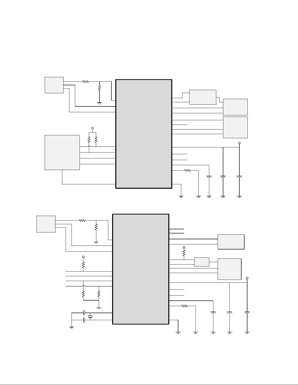
2.6 Example Applications
Embedded
Device
SOC
USB2422
SMBCLK
SMBDATA
RESET_N
XTALOUT
XTALIN
SUSP_IND
RBIAS
VDD33 (1,9,18)
PLLFILT
CRFILT
N/C
PRTPWR1
OCS1_N
USBDP_DN1
USBDM_DN1
PRTPWR2(11)
OCS2_N(12)
USBDP_DN2
USBDM_DN2
GND
R
BIAS
C
BYPCOUTCRCOUTPLL
Vcc
USB Switch
Enable
FAULT_N
RESET_N
Clock
VBUS_DET
USBDP_UP
USBDM_UP
Connector
3.3V
USB
Connector
R
VBUS
R
VBUS
USB2422
VBUS_DET
USBDP_UP
USBDM_UP
CFG_SEL0(14)
NON_REM1(13)
RESET_N
XTAL1(22)
XTAL2(21)
NON_REM0(17)
RBIAS
VDD33 (1,9,18)
PLLFILT
CRFILT
N/C
PRTPWR2(11)
OCS2_N(12)
USBDP_DN2
USBDM_DN2
PRTPWR1
OCS1_N
USBDP_DN1
USBDM_DN1
GND
R2
R2
R
BIAS
C
BYP
C
OUTCR
C
OUTPLL
USB
Connector
Charger
Enabled
Port
Non-removable
Device
R
VBUS
R
VBUS
R2
Vcc
Vcc
R1
Vcc
24MHz
Power
Switch
Cx
Cx
Figure 2.5 and Figure 2.6 depict example applications for an SoC based design and a non-SoC based
design, respectively. The corresponding resistor and capacitor values for these examples are provided
in Ta b le 2 .5 .
2-Port USB 2.0 Hi-Speed Hub Controller
Datasheet
Figure 2.5 Example Application - SoC Based Design
DS00001726A-page 16 2014 Microchip Technology Inc.
Figure 2.6 Example Application - Non-SoC Based Design
Page 17

2-Port USB 2.0 Hi-Speed Hub Controller
Datasheet
Table 2.5 Example Applications - Resistor/Capacitor Values
DESIGNATOR VALUE
R1 20 kΩ
R2 50 kΩ
Cx 18 pF
Note 2.1 C
Note 2.2 C
C
BYP
C
OUTCR
C
OUTPLL
R
BIAS
R
VBUS
should be placed as close as possible to pin 9
OUTCR
should be placed as close as possible to pin 1
OUTPLL
1.0 uF
1.0 uF
(Note 2.1)
0.1 uF
(Note 2.2)
12 kΩ
100 kΩ
2014 Microchip Technology Inc. DS00001726A-page 17
Page 18
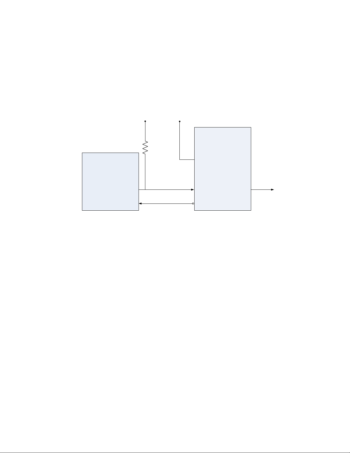
Chapter 3 Battery Charging Support
USB2422
USB Port Power
Controller
IN
EN
FLAG
VBUS
5.0 V3.3 V
R
STRAP
PRTPWR1
OCSx_N
The USB2422 hub provides support for battery charging devices on a per port basis in compliance
with the USB Battery Charging Specification, Revision 1.1. The hub can be configured to individually
enable each downstream port for battery charging support either via pin strapping (Port 1 only) as
illustrated in Figure 3.1 or by setting the corresponding configuration bits via SMBus (Section 4.1 on
page 20).
2-Port USB 2.0 Hi-Speed Hub Controller
Datasheet
Figure 3.1 Battery Charging via External Power Supply
Note: R
enables battery charging.
STRAP
3.1 USB Battery Charging
A downstream port enabled for battery charging turns on port power as soon as the power on reset
and hardware configuration process has completed. The hub does not need to be enumerated nor
does VBUS_DET need to be asserted for the port power to be enabled. These conditions allow battery
charging in S3, S4, and S5 system power states as well as in the fully operational state. The USB
Battery Charging Specification does not interfere with standard USB operation, which allows a device
to perform battery charging at any time.
A port that supports battery charging must be able to support 1.5 amps of current on VBUS. Standard
USB port power controllers typically only allow for 0.8 amps of current before detecting an over-current
condition. Therefore, the 5 volt power supply, port power controller, or over-current protection devices
must be chosen to handle the larger current demand compared to standard USB hub designs.
3.1.1 Special Behavior of PRTPWR Pins
The USB2422 enables VBUS by asserting the port power (PRTPWR[2:1]) as soon as the hardware
configuration process has completed. If the port detects an over-current condition, PRTPWR[2:1] will
be turned off to protect the circuitry from overloading. If an over-current condition is detected when the
hub is not enumerated, PRTPWR[2:1] can only be turned on from the host or if RESET_N is toggled.
These behaviors provide battery charging even when the hub is not enumerated and protect the hub
from sustained short circuit conditions. If the short circuit condition persists when the hub is plugged
into a host system the user is notified that a port has an over-current condition. Otherwise
PRTPWR[2:1] turned on by the host system and the ports operate normally.
DS00001726A-page 18 2014 Microchip Technology Inc.
Page 19

2-Port USB 2.0 Hi-Speed Hub Controller
Datasheet
3.2 Battery Charging Configuration
The battery charging option can be configured in one of two ways:
When the hub is brought up in the default configuration with strapping options enabled, with the
PRTPWR1/BC_EN1 pin configured (Port 1 only). See the following sections for details:
Section 2.3: Pin Descriptions (Grouped by Function) on page 11
Section 2.5: Strap Pin Configuration on page 14
When the hub is initialized for configuration over SMBus.
3.2.1 Battery Charging Enabled via SMBus
Register memory map location 0xD0 is allocated for battery charging support. The Battery Charging
register at location 0xD0 starting from bit 1 enables battery charging for each downstream port when
asserted. Bit 1 represents port 1, and bit 2 represents port 2. Each port that has battery charging
enabled asserts the corresponding PRTPWR[2:1] pin.
2014 Microchip Technology Inc. DS00001726A-page 19
Page 20

Chapter 4 Configuration Options
Microchip’s USB 2.0 hub is fully compliant with the USB Specification [1]. Refer to Chapter 10 (Hub
Specification) for general details regarding hub operation and functionality.
The hub provides one Transaction Translator (TT) that is shared by both downstream ports (defined
as Single-TT configuration). The TT contains 4 non-periodic buffers.
4.1 Hub Configuration
The USB2422 only supports internal defaults with the exception of the non-removable strap option
(using NON_REM[1:0]). The hub internal default settings are as follows:
Internal Default Configuration without over-rides
Strap options enabled
Self-powered operation enabled
Individual power switching
Individual over-current sensing
2-Port USB 2.0 Hi-Speed Hub Controller
Datasheet
Table 4.1 Hub Configuration Options
CFG_SEL DESCRIPTION
0 Default configuration:
Strap options enabled
Hub descriptors indicate the hub as “self-powered”
1 The hub is configured externally over SMBus (as an SMBus
slave device with address 0101100b):
Strap options disabled
Self-powered or bus-powered depending on register
settings
All registers configured over SMBus
4.2 Resets
There are two device resets: a hardware reset via RESET_N, and a USB Bus Reset.
4.2.1 External Hardware RESET_N
A valid hardware reset is defined as assertion of RESET_N for a minimum of 1 μs after all power
supplies are within operating range. While reset is asserted, the hub (and its associated external
circuitry) consumes less than 500 μA of current from the upstream USB power source.
Assertion of RESET_N causes the following:
1. All downstream ports are disabled.
2. The PRTPWR power to downstream devices is turned on when battery charging is enabled for a
specific port, and removed when battery charging is disabled for a specific port.
3. The PHYs are disabled, and the differential pairs will be in a high-impedance state.
4. All transactions immediately terminate; no states are saved.
5. All internal registers return to the default state (in most cases, 00h).
6. The external crystal oscillator is halted.
DS00001726A-page 20 2014 Microchip Technology Inc.
Page 21
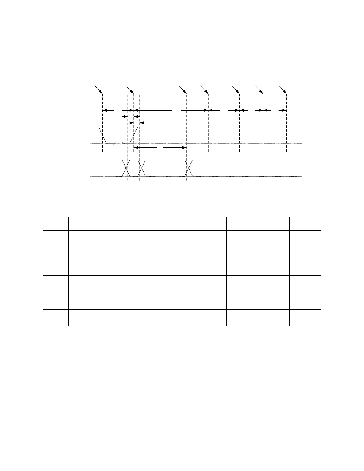
2-Port USB 2.0 Hi-Speed Hub Controller
t1
t4
t5
t6
t7 t8
Valid Driven by Hub if strap is an output
RESET_N
VSS
NON_REM[1:0]
VSS
Hardware
reset asserted
Read
NON_REM[1:0]
Drive Strap
Outputs to
inactive levels
Attach
USB
Upstream
Attach
Debounce
Interval Idle
Start completion
request response
t2
t3
Don’t Care
Don’t Care
Datasheet
7. The PLL is halted.
4.2.1.1 Hub Configuration Timing for Strapping Option
Figure 4.1 Hub Configuration Timing
Table 4.2 Hub Configuration Timing
NAME DESCRIPTION MIN TYP MAX UNITS
t1 RESET_N asserted 1 μsec
t2 Strap setup time 16.7 nsec
t3 Strap hold time 16.7 1400 nsec
t4 Hub outputs driven to inactive logic states 1.5 2 μsec
t5 USB attach (See Note) 3 μsec
t6 Host acknowledges attach and signals USB reset 100 msec
t7 USB idle undefined msec
t8 Completion time for requests (with or without data
5 msec
stage)
Note: All power supplies must have reached the operating levels mandated in Chapter 5, DC
Parameters, prior to (or coincident with) the assertion of RESET_N.
4.2.2 USB Bus Reset
In response to the upstream port signaling a reset to the hub, the hub does the following:
1. Sets default address to 0.
2. Sets configuration to unconfigured.
3. The PRTPWR power to downstream devices is turned on when battery charging is enabled for a
specific port, and removed when battery charging is disabled for a specific port.
4. Clears all TT buffers.
5. Moves device from suspended to active (if suspended).
2014 Microchip Technology Inc. DS00001726A-page 21
Page 22
6. Complies with Section 11.10 of the USB 2.0 Specification for behavior after completion of the reset
Denotes Master-to-Slave Denotes Slave-to-Master
S Slave Address Register AddressWr A
17118A1
...
181
Byte Count = N
A Data byte 1 A Data byte 2 A
81 1 188
Data byte N A P
sequence. The host then configures the hub and the hub’s downstream port devices in accordance
with the specification.
The hub does not propagate the upstream USB reset to downstream devices.
4.3 SMBus
The Microchip hub can be configured by an external processor via an SMBus interface (see Ta bl e 4. 1
for details on enabling the SMBus interface). The Microchip hub waits indefinitely for the SMBus code
load to complete and only appears as a newly connected device on USB after the code load is
complete.
The hub’s SMBus acts as a slave-only SMBus device. The implementation only supports block write
(Section 4.3.2.1) and block read (Section 4.3.2.2) protocols. Reference the System Management Bus
Specification [2] for additional information.
Refer to Section 4.4, "SMBus Registers," on page 24 for details on all SMBus accessible registers.
4.3.1 SMBus Slave Address
The 7-bit slave address is 0101100b. The hub will not respond to the general call address of 0000000b.
4.3.2 Protocol Implementation
Typical block write and block read protocols are shown in figures 4.2 and 4.3. Register accesses are
performed using 7-bit slave addressing, an 8-bit register address field, and an 8-bit data field. The
shading shown in the figures during a read or write indicates the hub is driving data on the SMBDATA
line; otherwise, host data is on the SMBDATA line.
The SMBus slave address assigned to the hub (0101100b) allows it to be identified on the SMBus.
The register address field is the internal address of the register to be accessed. The register data field
is the data that the host is attempting to write to the register or the contents of the register that the
host is attempting to read.
2-Port USB 2.0 Hi-Speed Hub Controller
Datasheet
Note: Data bytes are transferred MSB first.
4.3.2.1 Block Write/Read
The block write begins with a slave address and a write condition. After the command code, the host
issues a byte count which describes how many more bytes will follow in the message. If a slave had
20 bytes to send, the first byte would be the number 20 (14h), followed by the 20 bytes of data. The
byte count may not be zero. A block write or read allows a transfer maximum of 32 data bytes.
Note: For the following SMBus tables:
4.3.2.2 Block Read
A block read differs from a block write in that the repeated start condition exists to satisfy the SMBus
specification’s requirement for a change in the transfer direction.
Figure 4.2 Block Write
DS00001726A-page 22 2014 Microchip Technology Inc.
Page 23

2-Port USB 2.0 Hi-Speed Hub Controller
1
SS Slave Address Register AddressWr
1711 8A1
Slave Address Rd A
711
...
A
81 1 188 181
PA AAAByte Count = N Data byte 2Data byte 1 Data byte N
Datasheet
Figure 4.3 Block Read
4.3.2.3 Invalid Protocol Response Behavior
Note that any attempt to update registers with an invalid protocol will not be updated. The only valid
protocols are write block and read block (described above), where the hub only responds to the 7-bit
hardware selected slave address (0101100b).
4.3.3 Slave Device Timeout
Devices in a transfer can abort the transfer in progress and release the bus when any single clock low
interval exceeds 25 ms (T
condition within or after the transfer of the interrupted data byte. Slave devices must reset their
TIMEOUT, MIN
communication and be able to receive a new START condition no later than 35 ms (T
Note: Some simple devices do not contain a clock low drive circuit; this simple kind of device typically
resets its communications port after a start or stop condition. The slave device timeout must
be implemented.
). The master must detect this condition and generate a stop
TIMEOUT, MAX
).
4.3.4 Stretching the SCLK Signal
The hub supports stretching of the SCLK by other devices on the SMBus. However, the hub does not
stretch the SCLK.
4.3.5 SMBus Timing
The SMBus slave interface complies with the SMBus Specification Revision 1.0 [2]. See Section 2.1,
AC Specifications on page 3 for more information.
4.3.6 Bus Reset Sequence
The SMBus slave interface resets and returns to the idle state upon a START condition followed
immediately by a STOP condition.
4.3.7 SMBus Alert Response Address
The SMBALERT# signal is not supported by the hub.
2014 Microchip Technology Inc. DS00001726A-page 23
Page 24

4.4 SMBus Registers
This section details the device SMBus registers.
Note: Internal Default ROM values are not visible to THE SMBus interface and cannot be read. When
the hub is configured for SMBus register load, the entire register set must be written.
Table 4.3 Internal Default and SMBus Register Memory Map
2-Port USB 2.0 Hi-Speed Hub Controller
Datasheet
INTERNAL
REG.
ADDRESS TYPE REGISTER NAME
00h R/W Vendor ID Least Significant Bit Register (VIDL) 24h 00h
01h R/W Vendor ID Most Significant Bit Register (VIDM) 04h 00h
02h R/W Product ID Least Significant Bit Register (PIDL) 22h 00h
03h R/W Product ID Most Significant Bit Register (PIDM) 24h 00h
04h R/W Device ID Least Significant Bit Register (DIDL) A0h 00h
05h R/W Device ID Most Significant Bit Register (DIDM) 00h 00h
06h R/W Configuration Data Byte 1 Register (CFG1) 8Bh 00h
07h R/W Configuration Data Byte 2 Register (CFG2) 20h 00h
08h R/W Configuration Data Byte 3 Register (CFG3) 02h 00h
09h R/W Non-Removable Device Register (NRD) 00h 00h
0Ah R/W Port Disable for Self-Powered Operation Register (PDS) 00h 00h
0Bh R/W Port Disable for Bus-Powered Operation Register (PDB) 00h 00h
0Ch R/W Max Power for Self-Powered Operation Register (MAXPS) 01h 00h
0Dh R/W Max Power for Bus-Powered Operation Register (MAXPB) 32h 00h
DEFAULT
ROM
SMBUS &
EEPROM
DEFAULT
0Eh R/W Hub Controller Max Current for Self-Powered Operation Register
0Fh R/W Hub Controller Max Power for Bus-Powered Operation Register
10h R/W Power-On Time Register (PWRT) 32h 00h
11h R/W Language ID High Register (LANGIDH) 00h 00h
12h R/W Language ID Low Register (LANGIDL) 00h 00h
13h R/W Manufacturer String Length Register (MFRSL) 00h 00h
14h R/W Product String Length Register (PRDSL) 00h 00h
15h R/W Serial String Length Register (SERSL) 00h 00h
16h-53h R/W Manufacturer String Registers (MANSTR) 00h 00h
54h-91h R/W Product String Registers (PRDSTR) 00h 00h
92h-CFh R/W Serial String Registers (SERSTR) 00h 00h
D0h R/W Battery Charging Enable Register (BC_EN) 00h 00h
E0h-F5h - RESERVED - -
DS00001726A-page 24 2014 Microchip Technology Inc.
(HCMCS)
(HCMCB)
01h 00h
32h 00h
Page 25

2-Port USB 2.0 Hi-Speed Hub Controller
Datasheet
Table 4.3 Internal Default and SMBus Register Memory Map (continued)
REG.
ADDRESS TYPE REGISTER NAME
F6h R/W Boost Upstream Register (BOOSTUP) 00h 00h
F7h - RESERVED - -
F8h R/W Boost Downstream Register (BOOST40) 00h 00h
F9h - RESERVED - -
FAh R/W Port Swap Register (PRTSP) 00h 00h
FBh R/W Port 1/2 Remap Register (PRTR12) 00h 00h
FCh-FEh - RESERVED - -
FFh R/W Status/Command Register (STCD) 00h 00h
DEFAULT
ROM
4.4.1 Vendor ID Least Significant Bit Register (VIDL)
Offset: 00h Size: 8 bits
INTERNAL
SMBUS &
EEPROM
DEFAULT
BITS DESCRIPTION TYPE DEFAULT
7:0 Least Significant Byte of the Vendor ID (VID_LSB)
R/W 00h
This is a 16-bit value that uniquely identifies the Vendor of the user device
(assigned by USB-Interface Forum). This field is set by the OEM using the
SMBus interface option.
4.4.2 Vendor ID Most Significant Bit Register (VIDM)
Address: 01h Size: 8 bits
BITS DESCRIPTION TYPE DEFAULT
7:0 Most Significant Byte of the Vendor ID (VID_LSB)
This is a 16-bit value that uniquely identifies the Vendor of the user device
(assigned by USB-Interface Forum). This field is set by the OEM using the
SMBus interface options.
R/W 00h
2014 Microchip Technology Inc. DS00001726A-page 25
Page 26

2-Port USB 2.0 Hi-Speed Hub Controller
Datasheet
4.4.3 Product ID Least Significant Bit Register (PIDL)
Address: 02h Size: 8 bits
BITS DESCRIPTION TYPE DEFAULT
7:0 Least Significant Byte of the Product ID (PID_LSB)
This is a 16-bit value that the Vendor can assign that uniquely identifies this
particular product (assigned by OEM). This field is set by the OEM using the
SMBus interface options.
R/W 00h
4.4.4 Product ID Most Significant Bit Register (PIDM)
Address: 03h Size: 8 bits
BITS DESCRIPTION TYPE DEFAULT
7:0 Most Significant Byte of the Product ID (PID_LSB)
This is a 16-bit value that the Vendor can assign that uniquely identifies this
particular product (assigned by OEM). This field is set by the OEM using
either SMBus interface options.
R/W 00h
4.4.5 Device ID Least Significant Bit Register (DIDL)
Address: 04h Size: 8 bits
BITS DESCRIPTION TYPE DEFAULT
7:0 Least Significant Byte of the Device ID (DID_LSB)
This is a 16-bit device release number in BCD format (assigned by OEM).
This field is set by the OEM using either the SMBus interface options.
R/W 00h
4.4.6 Device ID Most Significant Bit Register (DIDM)
Address: 05h Size: 8 bits
BITS DESCRIPTION TYPE DEFAULT
7:0 Most Significant Byte of the Device ID (DID_LSB)
This is a 16-bit device release number in BCD format (assigned by OEM).
This field is set by the OEM using the SMBus interface options.
DS00001726A-page 26 2014 Microchip Technology Inc.
R/W 00h
Page 27

2-Port USB 2.0 Hi-Speed Hub Controller
Datasheet
4.4.7 Configuration Data Byte 1 Register (CFG1)
Address: 06h Size: 8 bits
BITS DESCRIPTION TYPE DEFAULT
7 Self or Bus Power (SELF_BUS_PWR)
R/W 0b
Selects between Self- and Bus-Powered operation.
The Hub is either Self-Powered (draws less than 2mA of upstream bus
power) or Bus-Powered (limited to a 100mA maximum of upstream power
prior to being configured by the host controller).
When configured as a Bus-Powered device, the Hub consumes less than
100mA of current prior to being configured. After configuration, the BusPowered Hub (along with all associated hub circuitry, any embedded
devices if part of a compound device, and 100mA per externally available
downstream port) must consume no more than 500mA of upstream VBUS
current. The current consumption is system dependent, and the OEM must
ensure that the USB2.0 specifications are not violated.
When configured as a Self-Powered device, <1mA of upstream VBUS
current is consumed and all ports are available, with each port being
capable of sourcing 500mA of current.
This field is set by the OEM using the SMBus interface option.
Please see the description under Dynamic Power for the self/bus power
functionality when dynamic power switching is enabled.
0 = Bus-Powered operation
1 = Self-Powered operation
Note: If Dynamic Power Switching is enabled, this bit is ignored and the
LOCAL_PWR pin is used to determine if the hub is operating from
self or bus power.
6 RESERVED --
5 High Speed Disable (HS_DISABLE)
R/W 0b
Disables the capability to attach as either a High/Full- speed device, and
forces attachment as Full-speed only i.e. (no High-Speed support).
0 = High-/Full-Speed
1 = Full-Speed-Only (High-Speed disabled)
4 Multi-TT Enable (MTT_ENABLE)
R/W 0b
Enables one transaction translator per port operation.
Selects between a mode where only one transaction translator is available
for all ports (Single-TT), or each port gets a dedicated transaction translator
(Multi-TT)
Note: The host may force Single-TT mode only
0 = Single TT for all ports. Default to STT if MTT still exists
1 = One TT per port (multiple TT’s supported)
2014 Microchip Technology Inc. DS00001726A-page 27
Page 28

2-Port USB 2.0 Hi-Speed Hub Controller
Datasheet
BITS DESCRIPTION TYPE DEFAULT
3 EOP Disable (EOP_DISABLE)
Disables EOP generation of EOF1 when in Full-Speed mode. During FS
operation only, this permits the Hub to send EOP if no downstream traffic is
detected at EOF1. See Section 11.3.1 of the USB 2.0 Specification for
additional details.
Note: generation of an EOP at the EOF1 point may prevent a Host
controller (operating in FS mode) from placing the USB bus in
suspend.
0 = An EOP is generated at the EOF1 point if no traffic is detected
1 = EOP generation at EOF1 is disabled (Note: This is normal USB
operation)
Note: This is a rarely used feature in the PC environment. It is included
because it is a permitted feature in Chapter 11 of the USB
specification.
2:1 Over Current Sense (CURRENT_SNS)
Selects current sensing on a port-by-port basis, all ports ganged, or none
(only for bus-powered hubs) The ability to support current sensing on a port
or ganged basis is hardware implementation dependent.
00 = Ganged sensing (all ports together)
01 = Individual port-by-port
1x = Over current sensing not supported (Must only be used with BusPowered configurations)
0 Port Power Switching (PORT_PWR)
Enables power switching on all ports simultaneously (ganged), or port power
is individually switched on and off on a port- by-port basis (individual). The
ability to support power enabling on a port or ganged basis is hardware
implementation dependent.
R/W 0b
R/W 00b
R/W 0b
0 = Ganged switching (all ports together)
1 = Individual port-by-port switching
DS00001726A-page 28 2014 Microchip Technology Inc.
Page 29

2-Port USB 2.0 Hi-Speed Hub Controller
Datasheet
4.4.8 Configuration Data Byte 2 Register (CFG2)
Address: 07h Size: 8 bits
BITS DESCRIPTION TYPE DEFAULT
7 Dynamic Power Enable (DYNAMIC)
R/W 0b
Controls the ability of the Hub to automatically change from Self-Powered
operation to Bus- Powered operation if the local power source is removed
or is unavailable (and from Bus-Powered to Self-Powered if the local power
source is restored).
Note: If the local power source is available, the Hub will always switch to
Self-Powered operation.
When Dynamic Power switching is enabled, the Hub detects the availability
of a local power source by monitoring the external LOCAL_PWR pin. If the
Hub detects a change in power source availability, the Hub immediately
disconnects and removes power from all downstream devices and
disconnects the upstream port. The Hub will then re-attach to the upstream
port as either a Bus-Powered Hub (if local-power is unavailable) or a SelfPowered Hub (if local power is available).
0 = No Dynamic auto-switching
(pin becomes SUSP_IND) and the hub controller will utilize the inverse of
the SELF_BUS_PWR bit for 'Hub_Status_Field' bit '0' (local power source)
1 = Dynamic Auto-switching capable
(pin becomes LOCAL_PWR) and the hub controller will utilize the
LOCAL_PWR pin for 'Hub_Status_Field' bit '0' (local power source)
6 RESERVED --
5:4 Over Current Timer Delay (OC_TIMER)
R/W 00b
00 = 0.1ms
01 = 4ms
10 = 8ms
11 = 16ms
3 Compound Device (COMPOUND)
R/W 0b
Allows the OEM to indicate that the Hub is part of a compound (see the USB
Specification for definition) device. The applicable port(s) must also be
defined as having a “Non-Removable Device”.
Note: When configured via strapping options, declaring a port as non-
removable automatically causes the hub controller to report that it
is part of a compound device.
0 = No
1 = Yes, Hub is part of a compound device
2:0 RESERVED --
2014 Microchip Technology Inc. DS00001726A-page 29
Page 30

2-Port USB 2.0 Hi-Speed Hub Controller
Datasheet
4.4.9 Configuration Data Byte 3 Register (CFG3)
Address: 08h Size: 8 bits
BITS DESCRIPTION TYPE DEFAULT
7:4 RESERVED --
3 Port Remapping Enable (PRTMAP_EN)
Selects the method used by the hub to assign port numbers and disable
ports
0 = Standard Mode
Strap options or the following registers are used to define which ports are
enabled, and the ports are mapped as Port'n' on the hub is reported as
Port'n' to the host, unless one of the ports is disabled, then the higher
numbered ports are remapped in order to report contiguous port numbers to
the host.
Register 0Ah: Port Disable For Self Powered Operation (Reset = 0x00)
Register 0Bh: Port Disable For Bus Powered Operation (Reset = 0x00).
1 = Port Re-Map mode
The mode enables remapping via Register FBh: Port Remap 12
2:1 RESERVED --
0 String Enable (STRING_EN)
Enables string descriptor support.
0 = String support disabled
1 = String support enabled
R/W 0b
R/W 0b
4.4.10 Non-Removable Device Register (NRD)
Address: 09h Size: 8 bits
BITS DESCRIPTION TYPE DEFAULT
7:0 Non-Removable Device (NR_DEVICE)
Indicates which port(s) include non- removable devices.
0 = port is removable
1 = port is non- removable
Informs the Host if one of the active physical ports has a permanent device
that is undetachable from the Hub.
Note: The device must provide its own descriptor data.
When using the internal default option, the NON_REM[1:0] pins will
designate the appropriate ports as being non- removable.
Bit 7= Reserved
Bit 6= Reserved
Bit 5= Reserved
Bit 4= Reserved
Bit 3= Reserved
Bit 2= Port 2 non-removable
Bit 1= Port 1 non removable
Bit 0= Reserved
DS00001726A-page 30 2014 Microchip Technology Inc.
R/W 00h
Page 31

2-Port USB 2.0 Hi-Speed Hub Controller
Datasheet
4.4.11 Port Disable for Self-Powered Operation Register (PDS)
Address: 0Ah Size: 8 bits
BITS DESCRIPTION TYPE DEFAULT
7:0 Port Disable Self-Powered (PORT_DIS_SP)
Disables 1 or more ports.
0 = port is available
1 = port is disabled
During Self-Powered operation, when PRTMAP_EN = '0', this selects the
ports which will be permanently disabled, and are not available to be
enabled or enumerated by a Host Controller. The ports can be disabled in
any order, the internal logic will automatically report the correct number of
enabled ports to the USB Host, and will reorder the active ports in order to
ensure proper function.
When using the internal default option, the PRT_DIS[1:0] pins will disable
the appropriate ports.
Bit 7= Reserved
Bit 6= Reserved
Bit 5= Reserved
Bit 4= Reserved
Bit 3= Reserved
Bit 2= Port 2 Disable
Bit 1= Port 1 Disable
Bit 0= Reserved
R/W 00h
4.4.12 Port Disable for Bus-Powered Operation Register (PDB)
Address: 0Bh Size: 8 bits
BITS DESCRIPTION TYPE DEFAULT
7:0 Port Disable Bus-Powered (PORT_DIS_BP)
2014 Microchip Technology Inc. DS00001726A-page 31
Disables 1 or more ports.
0 = port is available
1 = port is disabled
During Bus-Powered operation, when PRTMAP_EN = '0', this selects the
ports which will be permanently disabled, and are not available to be
enabled or enumerated by a Host Controller. The ports can be disabled in
any order, the internal logic will automatically report the correct number of
enabled ports to the USB Host, and will reorder the active ports in order to
ensure proper function.
When using the internal default option, the PRT_DIS[1:0] pins will disable
the appropriate ports.
Bit 7= Reserved
Bit 6= Reserved
Bit 5= Reserved
Bit 4= Reserved
Bit 3= Reserved
Bit 2= Port 2 Disable
Bit 1= Port 1 Disable
Bit 0= Reserved
R/W 00h
Page 32

2-Port USB 2.0 Hi-Speed Hub Controller
Datasheet
4.4.13 Max Power for Self-Powered Operation Register (MAXPS)
Address: 0Ch Size: 8 bits
BITS DESCRIPTION TYPE DEFAULT
7:0 Max Power Self-Powered (MAX_PWR_SP)
Value in 2mA increments that the Hub consumes from an upstream port
(VBUS) when operating as a self-powered hub. This value includes the hub
silicon along with the combined power consumption (from VBUS) of all
associated circuitry on the board. This value also includes the power
consumption of a permanently attached peripheral if the hub is configured
as a compound device, and the embedded peripheral reports 0mA in its
descriptors.
Note: The USB2.0 Specification does not permit this value to exceed
100mA.
R/W 00h
4.4.14 Max Power for Bus-Powered Operation Register (MAXPB)
Address: 0Dh Size: 8 bits
BITS DESCRIPTION TYPE DEFAULT
7:0 Max Power Bus-Powered (MAX_PWR_BP)
Value in 2mA increments that the Hub consumes from an upstream port
(VBUS) when operating as a self-powered hub. This value includes the hub
silicon along with the combined power consumption (from VBUS) of all
associated circuitry on the board. This value also includes the power
consumption of a permanently attached peripheral if the hub is configured
as a compound device, and the embedded peripheral reports 0mA in its
descriptors.
R/W 00h
4.4.15 Hub Controller Max Current for Self-Powered Operation Register (HCMCS)
Address: 0Eh Size: 8 bits
BITS DESCRIPTION TYPE DEFAULT
7:0 Hub Controller Max Current Self-Powered (HC_MAX_C_SP)
Value in 2mA increments that the Hub consumes from an upstream port
(VBUS) when operating as a self- powered hub. This value includes the hub
silicon along with the combined power consumption (from VBUS) of all
associated circuitry on the board. This value does NOT include the power
consumption of a permanently attached peripheral if the hub is configured
as a compound device.
Note: The USB2.0 Specification does not permit this value to exceed
100mA.
DS00001726A-page 32 2014 Microchip Technology Inc.
R/W 00h
Page 33

2-Port USB 2.0 Hi-Speed Hub Controller
Datasheet
4.4.16 Hub Controller Max Power for Bus-Powered Operation Register (HCMCB)
Address: 0Fh Size: 8 bits
BITS DESCRIPTION TYPE DEFAULT
7:0 Hub Controller Max Power Bus-Powered (MAX_PWR_BP)
Value in 2mA increments that the Hub consumes from an upstream port
(VBUS) when operating as a bus- powered hub. This value will include the
hub silicon along with the combined power consumption (from VBUS) of all
associated circuitry on the board. This value will NOT include the power
consumption of a permanently attached peripheral if the hub is configured
as a compound device.
R/W 00h
4.4.17 Power-On Time Register (PWRT)
Address: 10h Size: 8 bits
BITS DESCRIPTION TYPE DEFAULT
7:0 Power-On Time (POWER_ON_TIME)
The length of time that is takes (in 2 ms intervals) from the time the host
initiated power-on sequence begins on a port until power is good on that
port. System software uses this value to determine how long to wait before
accessing a powered-on port.
R/W 00h
4.4.18 Language ID High Register (LANGIDH)
Address: 11h Size: 8 bits
BITS DESCRIPTION TYPE DEFAULT
7:0 USB Language ID High (LANG_ID_H)
Upper 8 bits of the 16-bit language ID field.
R/W 00h
4.4.19 Language ID Low Register (LANGIDL)
Address: 12h Size: 8 bits
BITS DESCRIPTION TYPE DEFAULT
7:0 USB Language ID Low (LANG_ID_L)
2014 Microchip Technology Inc. DS00001726A-page 33
Lower 8 bits of the 16-bit language ID field.
R/W 00h
Page 34

2-Port USB 2.0 Hi-Speed Hub Controller
Datasheet
4.4.20 Manufacturer String Length Register (MFRSL)
Address: 13h Size: 8 bits
BITS DESCRIPTION TYPE DEFAULT
7:0 Manufacturer String Length (MFR_STR_LEN)
Maximum string length is 31 characters.
R/W 00h
4.4.21 Product String Length Register (PRDSL)
Address: 14h Size: 8 bits
BITS DESCRIPTION TYPE DEFAULT
7:0 Product String Length (PRD_STR_LEN)
Maximum string length is 31 characters.
R/W 00h
4.4.22 Serial String Length Register (SERSL)
Address: 15h Size: 8 bits
BITS DESCRIPTION TYPE DEFAULT
7:0 Serial String Length (SER_STR_LEN)
Maximum string length is 31 characters.
R/W 00h
4.4.23 Manufacturer String Registers (MANSTR)
Address: 16h-53h Size: 8 bits
BITS DESCRIPTION TYPE DEFAULT
7:0 Manufacturer String (MFR_STR)
UNICODE UTF-16LE per USB 2.0 Specification.
Maximum string length is 31 characters (62 Bytes).
Note: The String consists of individual 16 Bit UNICODE UTF-16LE
characters. The Characters will be stored starting with the LSB at
the least significant address and the MSB at the next 8-bit location
(subsequent characters must be stored in sequential contiguous
address in the same LSB, MSB manner).
DS00001726A-page 34 2014 Microchip Technology Inc.
R/W 00h
Page 35

2-Port USB 2.0 Hi-Speed Hub Controller
Datasheet
4.4.24 Product String Registers (PRDSTR)
Address: 54h-91h Size: 8 bits
BITS DESCRIPTION TYPE DEFAULT
7:0 Product String (PRD_STR)
UNICODE UTF-16LE per USB 2.0 Specification.
Maximum string length is 31 characters (62 Bytes).
Note: The String consists of individual 16 Bit UNICODE UTF-16LE
characters. The Characters will be stored starting with the LSB at
the least significant address and the MSB at the next 8-bit location
(subsequent characters must be stored in sequential contiguous
address in the same LSB, MSB manner).
R/W 00h
4.4.25 Serial String Registers (SERSTR)
Address: 92h-CFh Size: 8 bits
BITS DESCRIPTION TYPE DEFAULT
7:0 Serial String (SER_STR)
UNICODE UTF-16LE per USB 2.0 Specification.
Maximum string length is 31 characters (62 Bytes).
Note: The String consists of individual 16 Bit UNICODE UTF-16LE
characters. The Characters will be stored starting with the LSB at
the least significant address and the MSB at the next 8-bit location
(subsequent characters must be stored in sequential contiguous
address in the same LSB, MSB manner).
R/W 00h
4.4.26 Battery Charging Enable Register (BC_EN)
Address: D0h Size: 8 bits
BITS DESCRIPTION TYPE DEFAULT
7:0 Battery Charging Enable (BC_EN)
2014 Microchip Technology Inc. DS00001726A-page 35
Enables the battery charging feature for the corresponding port.
0 = Battery Charging support is not enabled
1 = Battery charging support is enabled
Bit 7= Reserved
Bit 6= Reserved
Bit 5= Reserved
Bit 4= Reserved
Bit 3= Reserved
Bit 2= Port 2 Battery Charging Enable
Bit 1= Port 1 Battery Charging Enable
Bit 0= Reserved
R/W 00h
Page 36

2-Port USB 2.0 Hi-Speed Hub Controller
Datasheet
4.4.27 Boost Upstream Register (BOOSTUP)
Address: F6h Size: 8 bits
BITS DESCRIPTION TYPE DEFAULT
7:2 RESERVED --
1:0 Boost Upstream (BOOST_IOUT_A)
USB electrical signaling drive strength Boost Bit for Upstream Port 'A'.
00 = Normal electrical drive strength
01 = Elevated electrical drive strength (+4% boost)
10 = Elevated electrical drive strength (+8% boost)
11 = Elevated electrical drive strength (+12% boost)
R/W 00b
4.4.28 Boost Downstream Register (BOOST40)
Address: F8h Size: 8 bits
BITS DESCRIPTION TYPE DEFAULT
7:4 RESERVED --
3:2 Boost Downstream Port 2 (BOOST_IOUT_2)
USB electrical signaling drive strength Boost Bit for Upstream Port '2'.
00 = Normal electrical drive strength
01 = Elevated electrical drive strength (+4% boost)
10 = Elevated electrical drive strength (+8% boost)
11 = Elevated electrical drive strength (+12% boost)
1:0 Boost Downstream Port 1 (BOOST_IOUT_1)
USB electrical signaling drive strength Boost Bit for Upstream Port '1'.
R/W 00b
R/W 00b
00 = Normal electrical drive strength
01 = Elevated electrical drive strength (+4% boost)
10 = Elevated electrical drive strength (+8% boost)
11 = Elevated electrical drive strength (+12% boost)
DS00001726A-page 36 2014 Microchip Technology Inc.
Page 37

2-Port USB 2.0 Hi-Speed Hub Controller
Datasheet
4.4.29 Port Swap Register (PRTSP)
Address: FAh Size: 8 bits
BITS DESCRIPTION TYPE DEFAULT
7:0 Port Swap (PRTSP)
Swaps the Upstream and Downstream USB DP and DM Pins for ease of
board routing to devices and connectors.
0 = USB D+ functionality is associated with the DP pin and Dfunctionality is associated with the DM pin.
1 = USB D+ functionality is associated with the DM pin and Dfunctionality is associated with the DP pin
Bit 7= Reserved
Bit 6= Reserved
Bit 5= Reserved
Bit 4= Reserved
Bit 3= Reserved
Bit 2= Port 2 DP/DM Swap
Bit 1= Port 1 DP/DM Swap
Bit 0= Upstream Port DP/DM Swap
R/W 00h
2014 Microchip Technology Inc. DS00001726A-page 37
Page 38

2-Port USB 2.0 Hi-Speed Hub Controller
Bits[7:4] = 0000 Physical Port 2 is disabled
0001 Physical Port 2 is mapped to Logical Port 1
0010 Physical Port 2 is mapped to Logical Port 2
0011
to
1111
RESERVED
Will default to 0000 value.
Bits[3:0] = 0000 Physical Port 1 is disabled
0001 Physical Port 1 is mapped to Logical Port 1
0010 Physical Port 1 is mapped to Logical Port 2
0011
to
1111
RESERVED
Will default to 0000 value.
Datasheet
4.4.30 Port 1/2 Remap Register (PRTR12)
Address: FBh Size: 8 bits
BITS DESCRIPTION TYPE DEFAULT
7:0 Port 1/2 Remap (PRTR12)
When a hub is enumerated by a USB Host Controller, the hub is only
permitted to report how many ports it has, the hub is not permitted to select
a numerical range or assignment. The Host Controller will number the
downstream ports of the hub starting with the number '1', up to the number
of ports that the hub reported as having.
The host's port number is referred to as “Logical Port Number” and the
physical port on the hub is the “Physical Port Number”. When remapping
mode is enabled (PRTMAP_EN in the Configuration Data Byte 3 Register
(CFG3)), the hub's downstream port numbers can be remapped to different
logical port numbers assigned by the host.
Note: The OEM must ensure that Contiguous Logical Port Numbers are
used, starting from one up to the maximum number of enabled
ports. This ensures that the hub's ports are numbered in
accordance with the way a Host will communicate with the ports.
R/W 00h
DS00001726A-page 38 2014 Microchip Technology Inc.
Page 39

2-Port USB 2.0 Hi-Speed Hub Controller
Datasheet
4.4.31 Status/Command Register (STCD)
Address: FFh Size: 8 bits
BITS DESCRIPTION TYPE DEFAULT
7:3 RESERVED --
2 SMBus Interface Power Down (INTF_PW_DN)
0 = Interface is active
1 = Interface power down after ACK has completed
Note: This bit is write once and is only cleared by assertion of the
external RESET_N pin.
1 Reset (RESET)
Resets the SMBus Interface and internal memory back to RESET_N
assertion default settings.
0 = Normal Run/Idle State
1 = Force a reset of the registers to their default state
Note: During this reset, this bit is automatically cleared to its default value
of 0.
0 USB Attach and Write Protect (USB_ATTACH)
0 = SMBus slave interface is active
1 = Hub will signal a USB attach event to an upstream device, and the
internal memory that is not Modify capable in the address range 00hFEh, is “write-protected” to prevent unintentional data corruption.
Note: This bit is write once and is only cleared by assertion of the
external RESET_N pin.
R/W 0b
R/W 0b
R/W 0b
2014 Microchip Technology Inc. DS00001726A-page 39
Page 40
2-Port USB 2.0 Hi-Speed Hub Controller
Chapter 5 DC Parameters
5.1 Maximum Guaranteed Ratings
PARAMETER SYMBOL MIN MAX UNITS COMMENTS
Datasheet
Storage Temperature T
Lead Temperature Refer to JEDEC Specification
3.3 V supply voltage VDD33 4.6 V
Voltage on any I/O pin -0.5 5.5 V
Voltage on XTALIN -0.5 4.0 V
Voltage on XTALOUT -0.5 2.5 V
Note 5.1 Refer to JEDEC Specification J-STD-020D [3].
Note 5.2 Stresses above the specified parameters could cause permanent damage to the device.
Note 5.3 When powering this device from laboratory or system power supplies, it is important that
STOR
This is a stress rating only and functional operation of the device at any condition above
those indicated in the operation sections of this specification is not implied.
the absolute maximum ratings not be exceeded or device failure can result. Some power
supplies exhibit voltage spikes on their outputs when the AC power is switched on or off.
In addition, voltage transients on the AC power line may appear on the DC output. When
this possibility exists, it is suggested that a clamp circuit be used.
-55 150 °C
J-STD-020D [3]
5.2 Operating Conditions
PARAMETER SYMBOL MIN MAX UNITS COMMENTS
USB2422 Operating
Temperature
USB2422-i Operating
Temperature
3.3 V supply voltage VDD33 3.0 3.6 V
3.3 V supply rise time t
Voltage on any I/O pin -0.3 5.5 V If any 3.3 V supply voltage drops
Voltage on XTALIN -0.3 VDD12
DS00001726A-page 40 2014 Microchip Technology Inc.
T
A
T
A
RT33
0 70 °C Ambient temperature in still air
-40 85 °C Ambient temperature in still air
0400μsSee Figure 5.1
below 3.0 V, then the MAX
becomes:
(3.3 V supply voltage) + 0.5
V
+ 0.3
Page 41
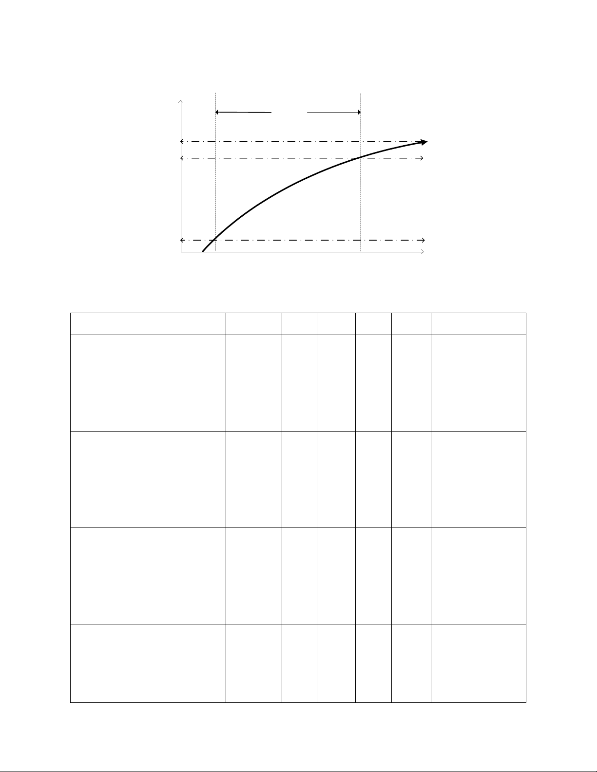
2-Port USB 2.0 Hi-Speed Hub Controller
t
10%
10%
90%
Voltage
t
RT33
t
90%
Time
100%
3.3 V
VSS
VDD33
Datasheet
Figure 5.1 Supply Rise Time Model
Table 5.1 DC Electrical Characteristics
PARAMETER SYMBOL MIN TYP MAX UNITS COMMENTS
I, IS Type Input Buffer
Low Input Level V
High Input Level V
Input Leakage I
Hysteresis (IS only) V
Input Buffer with Pull-Up (IPU)
Low Input Level V
High Input Level V
Low Input Leakage I
High Input Leakage I
Input Buffer with Pull-Down (IPD)
Low Input Level V
High Input Level V
Low Input Leakage I
High Input Leakage I
ILI
IHI
IL
HYSI
ILI
IHI
ILL
IHL
ILI
IHI
ILL
IHL
0.8 V TTL Levels
2.0 V
-10 +10 μAVIN = 0 to VDD33
250 350 mV
0.8 V TTL Levels
2.0 V
+35 +90 μAVIN = 0
-10 +10 μAVIN = VDD33
0.8 V TTL Levels
2.0 V
+10 -10 μAVIN = 0
-35 -90 μAVIN = VDD33
ICLK Input Buffer
Low Input Level V
High Input Level V
Input Leakage I
2014 Microchip Technology Inc. DS00001726A-page 41
ILCK
IHCK
IL
0.3 V
0.9 V
-10 +10 μAVIN = 0 to VDD33
Page 42

Table 5.1 DC Electrical Characteristics (continued)
PARAMETER SYMBOL MIN TYP MAX UNITS COMMENTS
O12, I/O12 & I/OSD12 Type Buffer
2-Port USB 2.0 Hi-Speed Hub Controller
Datasheet
Low Output Level V
High Output Level V
Output Leakage I
Hysteresis (SD pad only) V
Supply Current Unconfigured
Hi-Speed Host
Supply Current
Hi-Speed Host, each additional
downstream port
Supply Current
Hi-Speed Host, 1 downstream port
Supply Current
Hi-Speed Host, 2 downstream ports
Supply Current
Full-Speed Host, 1 downstream port
Supply Current
Full-Speed Host, 2 downstream ports
OL
OH
OL
HYSC
I
CCINTHS
I
CCINTFS
I
HCH1
I
HCH2
I
FCC1
I
FCC2
0.4 V IOL = 12 mA @
VDD33 = 3.3 V
2.4 V IOH = -12 mA @
VDD33 = 3.3 V
-10 +10 μA
250 350 mV VIN = VDD33
(Note 5.1)
40 45 mA
35 40 mA Note 5.8
47 58 mA Note 5.8
70 89
mA
Note 5.8
29 40 mA Note 5.8
35 45 mA Note 5.8
Supply Current Suspend I
Supply Current Reset I
Note 5.4 Output leakage is measured with the current pins in high impedance.
Note 5.5 See USB 2.0 Specification [1] for USB DC electrical characteristics.
Note 5.6 1000 μA for commercial temperature part, and 1200 μA for industrial temperature part.
Note 5.7 800 μA for commercial temperature part, and 1000 μA for industrial temperature part.
Note 5.8 Current measured during peak USB traffic and does not reflect the average current draw.
CSBY
CRST
425 Note
5.6
300 Note
5.7
μA
μA
DS00001726A-page 42 2014 Microchip Technology Inc.
Page 43

2-Port USB 2.0 Hi-Speed Hub Controller
Datasheet
5.2.1 Pin Capacitance
Table 5.2 Pin Capacitance
LIMITS
PARAMETER SYMBOL MIN TYP MAX UNIT TEST CONDITION
Clock Input
C
Capacitance
Input Capacitance C
Output Capacitance C
XTAL
IN
OUT
6 pF All pins except USB pins and the pins
under the test tied to AC ground.
6 pF Capacitance TA = 25°C
fc = 1 MHz
VDD33 = 3.3 V
6 pF The maximum capacitance values
include the full length of the pin pad.
2014 Microchip Technology Inc. DS00001726A-page 43
Page 44

Chapter 6 AC Specifications
C
1
C
2
C
L
Crystal
C
0
XTALIN
(C
S1
= CB1 + C
XTALIN
)
XTALOUT
(C
S2
= CB2 + C
XTALOUT
)
C1 = 2 x (CL – C0) – C
S1
C2 = 2 x (CL – C0) – C
S2
6.1 Oscillator/Crystal
Parallel Resonant, Fundamental Mode, 24 MHz ±350 ppm.
2-Port USB 2.0 Hi-Speed Hub Controller
Datasheet
Figure 6.1 Typical Crystal Circuit
Table 6.1 Crystal Circuit Legend
SYMBOL DESCRIPTION IN ACCORDANCE WITH
C
C
C
C
C
C
C
0
L
B
S
XTAL
1
2
Crystal shunt capacitance
Crystal load capacitance
Crystal manufacturer’s specification (See Note 6.1)
Total board or trace capacitance OEM board design
Stray capacitance Microchip IC and OEM board design
XTAL pin input capacitance Microchip IC
Load capacitors installed on OEM
board
Figure 6.2 Formula to Find the Value of C1 and C
Calculated values based on Figure 6.2, "Formula to Find the
Value of C1 and C2" (See Note 6.2)
2
Note 6.1 C0 is usually included (subtracted by the crystal manufacturer) in the specification for C
L
and should be set to 0 for use in the calculation of the capacitance formulas in Figure 6.2,
"Formula to Find the Value of C1 and C2". However, the PCB itself may present a parasitic
capacitance between XTALIN and XTALOUT. For an accurate calculation of C
take the parasitic capacitance between traces XTALIN and XTALOUT into account.
and C
1
2,
Note 6.2 Each of these capacitance values is typically approximately 18 pF.
DS00001726A-page 44 2014 Microchip Technology Inc.
Page 45

2-Port USB 2.0 Hi-Speed Hub Controller
Datasheet
6.2 External Clock
50% Duty cycle ± 10%, 24 MHz ± 350 ppm.
The external clock is recommended to conform to the signaling level designated in the JESD76-2
specification on 1.2 V CMOS Logic. XTALOUT should be treated as a weak (< 1 mA) buffer output.
6.2.1 USB 2.0
The Microchip hub conforms to all voltage, power, and timing characteristics and specifications as set
forth in the USB 2.0 Specification [1]. See the USB Specification for more information.
6.3 SMBus Interface
The Microchip hub conforms to all voltage, power, and timing characteristics and specifications as set
forth in the SMBus 1.0 Specification [2] for slave-only devices (except as noted in Section 4.3,
"SMBus," on page 22).
2014 Microchip Technology Inc. DS00001726A-page 45
Page 46

Chapter 7 Package Outline
2-Port USB 2.0 Hi-Speed Hub Controller
Datasheet
Note: For the most current package drawings,
see the Microchip Packaging Specification at
http://www.microchip.com/packaging
Figure 7.1 24-SQFN Package
DS00001726A-page 46 2014 Microchip Technology Inc.
Page 47

2-Port USB 2.0 Hi-Speed Hub Controller
Datasheet
Figure 7.2 Taping Dimensions and Part Orientation
2014 Microchip Technology Inc. DS00001726A-page 47
Page 48
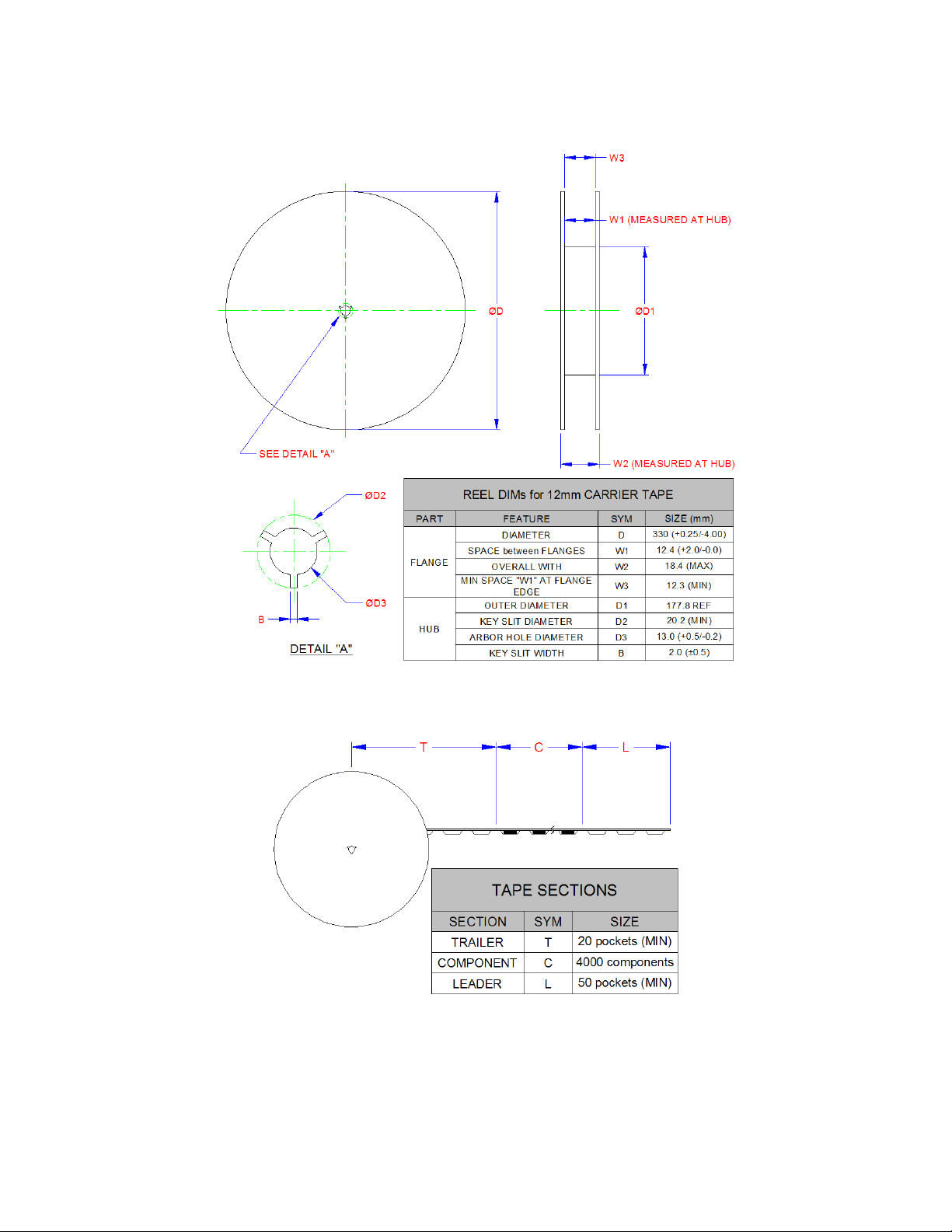
2-Port USB 2.0 Hi-Speed Hub Controller
Datasheet
Figure 7.3 Reel Dimensions
Figure 7.4 Tape Length and Part Quantity
Note: Standard reel size is 4000 pieces per reel.
DS00001726A-page 48 2014 Microchip Technology Inc.
Page 49

2-Port USB 2.0 Hi-Speed Hub Controller
Datasheet
Chapter 8 Datasheet Revision History
Table 8.1 Revision History
REVISION LEVEL & DATE SECTION/FIGURE/ENTRY CORRECTION
DS00001726A replaces the previous SMSC version rev. 1.0
Rev. 1.0 (06-04-13) Initial Revision
2014 Microchip Technology Inc. DS00001726A-page 49
Page 50

Appendix A (Acronyms)
OCS: Over-Current Sense
PCB: Printed Circuit Board
PHY: Physical Layer
PLL: Phase-Locked Loop
SQFN: Sawn Quad Flat No Leads
RoHS: Restriction of Hazardous Substances Directive
SCL: Serial Clock
SIE: Serial Interface Engine
SMBus: System Management Bus
TT: Transaction Translator
2-Port USB 2.0 Hi-Speed Hub Controller
Datasheet
DS00001726A-page 50 2014 Microchip Technology Inc.
Page 51

2-Port USB 2.0 Hi-Speed Hub Controller
Datasheet
Appendix B (References)
[1] Universal Serial Bus Specification, Version 2.0, April 27, 2000 (12/7/2000 and 5/28/2002 Errata)
USB Implementers Forum, Inc. http://www.usb.org
[2] System Management Bus Specification, version 1.0
SMBus. http://smbus.org/specs/
[3] JEDEC Specifications: JESD76-2 (June 2001) and J-STD-020D.1 (March 2008)
JEDEC Global Standards for the Microelectronics Industry.http://www.jedec.org/standards-documents
[4] USB Battery Charging Specification, Revision 1.1, April 15, 2009
USB Implementers Forum, Inc. http://www.usb.org
2014 Microchip Technology Inc. DS00001726A-page 51
Page 52

Note the following details of the code protection feature on Microchip devices:
CERTIFIED BY DNV
== ISO/TS 16949 ==
• Microchip products meet the specification contained in their particular Microchip Data Sheet.
• Microchip believes that its family of products is one of the most secure families of its kind on the market today, when used in the
intended manner and under normal conditions.
• There are dishonest and possibly illegal methods used to breach the code protection feature. All of these methods, to our
knowledge, require using the Microchip products in a manner outside the operating specifications contained in Microchip’s Data
Sheets. Most likely, the person doing so is engaged in theft of intellectual property.
• Microchip is willing to work with the customer who is concerned about the integrity of their code.
• Neither Microchip nor any other semiconductor manufacturer can guarantee the security of their code. Code protection does not
mean that we are guaranteeing the product as “unbreakable.”
Code protection is constantly evolving. We at Microchip are committed to continuously improving the code protection features of our
products. Attempts to break Microchip’s code protection feature may be a violation of the Digital Millennium Copyright Act. If such acts
allow unauthorized access to your software or other copyrighted work, you may have a right to sue for relief under that Act.
Information contained in this publication regarding device applications and the like is provided only for your convenience and may be
superseded by updates. It is your responsibility to ensure that your application meets with your specifications. MICROCHIP MAKES NO
REPRESENTATIONS OR WARRANTIES OF ANY KIND WHETHER EXPRESS OR IMPLIED, WRITTEN OR ORAL, STATUTORY OR
OTHERWISE, RELATED TO THE INFORMATION, INCLUDING BUT NOT LIMITED TO ITS CONDITION, QUALITY, PERFORMANCE,
MERCHANTABILITY OR FITNESS FOR PURPOSE
. Microchip disclaims all liability arising from this information and its use. Use of
Microchip devices in life support and/or safety applications is entirely at the buyer’s risk, and the buyer agrees to defend, indemnify and
hold harmless Microchip from any and all damages, claims, suits, or expenses resulting from such use. No licenses are conveyed, implicitly or otherwise, under any Microchip intellectual property rights.
Trademarks
The Microchip name and logo, the Microchip logo, dsPIC, FlashFlex, KEELOQ, KEELOQ logo, MPLAB, PIC, PICmicro, PICSTART, PIC32
logo, rfPIC, SST, SST Logo, SuperFlash and UNI/O are registered trademarks of Microchip Technology Incorporated in the U.S.A. and
other countries.
FilterLab, Hampshire, HI-TECH C, Linear Active Thermistor, MTP, SEEVAL and The Embedded Control Solutions Company are
registered trademarks of Microchip Technology Incorporated in the U.S.A.
Silicon Storage Technology is a registered trademark of Microchip Technology Inc. in other countries.
Analog-for-the-Digital Age, Application Maestro, BodyCom, chipKIT, chipKIT logo, CodeGuard, dsPICDEM, dsPICDEM.net,
dsPICworks, dsSPEAK, ECAN, ECONOMONITOR, FanSense, HI-TIDE, In-Circuit Serial Programming, ICSP, Mindi, MiWi, MPASM,
MPF, MPLAB Certified logo, MPLIB, MPLINK, mTouch, Omniscient Code Generation, PICC, PICC-18, PICDEM, PICDEM.net, PICkit,
PICtail, REAL ICE, rfLAB, Select Mode, SQI, Serial Quad I/O, Total Endurance, TSHARC, UniWinDriver, WiperLock, ZENA and ZScale are trademarks of Microchip Technology Incorporated in the U.S.A. and other countries.
SQTP is a service mark of Microchip Technology Incorporated in the U.S.A.
GestIC and ULPP are registered trademarks of Microchip Technology Germany II GmbH & Co. KG, a subsidiary of Microchip
Technology Inc., in other countries.
flexPWR, JukeBlox, Kleer, KleerNet, MediaLB, and MOST
The preceding is a non-exhaustive list of trademarks in use in the US and other countries. For a complete list of trademarks, email a
request to legal.department@microchip.com
. The absence of a trademark (name, logo, etc.) from the list does not constitute a waiver
of any intellectual property rights that SMSC has established in any of its trademarks.
All other trademarks mentioned herein are property of their respective companies.
© 2014, Microchip Technology Incorporated, Printed in the U.S.A., All Rights Reserved.
ISBN: 9781632761477
Microchip received ISO/TS-16949:2009 certification for its worldwide
QUALITY MANAGEMENT SYSTEM
DS00001726A-page 52 Advance Information 2014 Microchip Technology Inc.
headquarters, design and wafer fabrication facilities in Chandler and
Tempe, Arizona; Gresham, Oregon and design centers in California
and India. The Company’s quality system processes and procedures
are for its PIC
devices, Serial EEPROMs, microperipherals, nonvolatile memory and
analog products. In addition, Microchip’s quality system for the design
and manufacture of development systems is ISO 9001:2000 certified.
®
MCUs and dsPIC® DSCs, KEELOQ
®
code hopping
Page 53

Worldwide Sales and Service
AMERICAS
Corporate Office
2355 West Chandler Blvd.
Chandler, AZ 85224-6199
Tel: 480-792-7200
Fax: 480-792-7277
Technical Support:
http://www.microchip.com/
support
Web Address:
www.microchip.com
Atlanta
Duluth, GA
Tel: 678-957-9614
Fax: 678-957-1455
Austin, TX
Tel: 512-257-3370
Boston
Westborough, MA
Tel: 774-760-0087
Fax: 774-760-0088
Chicago
Itasca, IL
Tel: 630-285-0071
Fax: 630-285-0075
Cleveland
Independence, OH
Tel: 216-447-0464
Fax: 216-447-0643
Dallas
Addison, TX
Tel: 972-818-7423
Fax: 972-818-2924
Detroit
Novi, MI
Tel: 248-848-4000
Houston, TX
Tel: 281-894-5983
Indianapolis
Noblesville, IN
Tel: 317-773-8323
Fax: 317-773-5453
Los Angeles
Mission Viejo, CA
Tel: 949-462-9523
Fax: 949-462-9608
New York, NY
Tel: 631-435-6000
San Jose, CA
Tel: 408-735-9110
Canada - Toronto
Tel: 905-673-0699
Fax: 905-673-6509
ASIA/PACIFIC
Asia Pacific Office
Suites 3707-14, 37th Floor
Tower 6, The Gateway
Harbour City, Kowloon
Hong Kong
Tel: 852-2943-5100
Fax: 852-2401-3431
Australia - Sydney
Tel: 61-2-9868-6733
Fax: 61-2-9868-6755
China - Beijing
Tel: 86-10-8569-7000
Fax: 86-10-8528-2104
China - Chengdu
Tel: 86-28-8665-5511
Fax: 86-28-8665-7889
China - Chongqing
Tel: 86-23-8980-9588
Fax: 86-23-8980-9500
China - Hangzhou
Tel: 86-571-8792-8115
Fax: 86-571-8792-8116
China - Hong Kong SAR
Tel: 852-2943-5100
Fax: 852-2401-3431
China - Nanjing
Tel: 86-25-8473-2460
Fax: 86-25-8473-2470
China - Qingdao
Tel: 86-532-8502-7355
Fax: 86-532-8502-7205
China - Shanghai
Tel: 86-21-5407-5533
Fax: 86-21-5407-5066
China - Shenyang
Tel: 86-24-2334-2829
Fax: 86-24-2334-2393
China - Shenzhen
Tel: 86-755-8864-2200
Fax: 86-755-8203-1760
China - Wuhan
Tel: 86-27-5980-5300
Fax: 86-27-5980-5118
China - Xian
Tel: 86-29-8833-7252
Fax: 86-29-8833-7256
China - Xiamen
Tel: 86-592-2388138
Fax: 86-592-2388130
China - Zhuhai
Tel: 86-756-3210040
Fax: 86-756-3210049
ASIA/PACIFIC
India - Bangalore
Tel: 91-80-3090-4444
Fax: 91-80-3090-4123
India - New Delhi
Tel: 91-11-4160-8631
Fax: 91-11-4160-8632
India - Pune
Tel: 91-20-3019-1500
Japan - Osaka
Tel: 81-6-6152-7160
Fax: 81-6-6152-9310
Japan - Tokyo
Tel: 81-3-6880- 3770
Fax: 81-3-6880-3771
Korea - Daegu
Tel: 82-53-744-4301
Fax: 82-53-744-4302
Korea - Seoul
Tel: 82-2-554-7200
Fax: 82-2-558-5932 or
82-2-558-5934
Malaysia - Kuala Lumpur
Tel: 60-3-6201-9857
Fax: 60-3-6201-9859
Malaysia - Penang
Tel: 60-4-227-8870
Fax: 60-4-227-4068
Philippines - Manila
Tel: 63-2-634-9065
Fax: 63-2-634-9069
Singapore
Tel: 65-6334-8870
Fax: 65-6334-8850
Taiwan - Hsin Chu
Tel: 886-3-5778-366
Fax: 886-3-5770-955
Taiwan - Kaohsiung
Tel: 886-7-213-7830
Taiwan - Taipei
Tel: 886-2-2508-8600
Fax: 886-2-2508-0102
Thailand - Bangkok
Tel: 66-2-694-1351
Fax: 66-2-694-1350
EUROPE
Austria - Wels
Tel: 43-7242-2244-39
Fax: 43-7242-2244-393
Denmark - Copenhagen
Tel: 45-4450-2828
Fax: 45-4485-2829
France - Paris
Tel: 33-1-69-53-63-20
Fax: 33-1-69-30-90-79
Germany - Dusseldorf
Tel: 49-2129-3766400
Germany - Munich
Tel: 49-89-627-144-0
Fax: 49-89-627-144-44
Germany - Pforzheim
Tel: 49-7231-424750
Italy - Milan
Tel: 39-0331-742611
Fax: 39-0331-466781
Italy - Venice
Tel: 39-049-7625286
Netherlands - Drunen
Tel: 31-416-690399
Fax: 31-416-690340
Poland - Warsaw
Tel: 48-22-3325737
Spain - Madrid
Tel: 34-91-708-08-90
Fax: 34-91-708-08-91
Sweden - Stockholm
Tel: 46-8-5090-4654
UK - Wokingham
Tel: 44-118-921-5800
Fax: 44-118-921-5820
03/25/14
DS00001726A-page 53 2014 Microchip Technology Inc.
 Loading...