

Page 1

UCS81003
Evaluation Board
User’s Guide
2014 Microchip Technology Inc. DS50002300A
Page 2

Note the following details of the code protection feature on Microchip devices:
YSTEM
CERTIFIED BY DNV
== ISO/TS 16949 ==
• Microchip products meet the specification contained in their particular Microchip Data Sheet.
• Microchip believes that its family of products is one of the most secure families of its kind on the market today, when used in the
intended manner and under normal conditions.
• There are dishonest and possibly illegal methods used to breach the code protection feature. All of these methods, to our
knowledge, require using the Microchip products in a manner outside the operating specifications contained in Microchip’s Data
Sheets. Most likely, the person doing so is engaged in theft of intellectual property.
• Microchip is willing to work with the customer who is concerned about the integrity of their code.
• Neither Microchip nor any other semiconductor manufacturer can guarantee the security of their code. Code protection does not
mean that we are guaranteeing the product as “unbreakable.”
Code protection is constantly evolving. We at Microchip are committed to continuously improving the code protection features of our
products. Attempts to break Microchip’s code protection feature may be a violation of the Digital Millennium Copyright Act. If such acts
allow unauthorized access to your software or other copyrighted work, you may have a right to sue for relief under that Act.
Information contained in this publication regarding device
applications and the like is provided only for your convenience
and may be superseded by updates. It is your responsibility to
ensure that your application meets with your specifications.
MICROCHIP MAKES NO REPRESENTATIONS OR
WARRANTIES OF ANY KIND WHETHER EXPRESS OR
IMPLIED, WRITTEN OR ORAL, STATUTORY OR
OTHERWISE, RELATED TO THE INFORMATION,
INCLUDING BUT NOT LIMITED TO ITS CONDITION,
QUALITY, PERFORMANCE, MERCHANTABILITY OR
FITNESS FOR PURPOSE. Microchip disclaims all liability
arising from this information and its use. Use of Microchip
devices in life support and/or safety applications is entirely at
the buyer’s risk, and the buyer agrees to defend, indemnify and
hold harmless Microchip from any and all damages, claims,
suits, or expenses resulting from such use. No licenses are
conveyed, implicitly or otherwise, under any Microchip
intellectual property rights.
Trademarks
The Microchip name and logo, the Microchip logo, dsPIC,
FlashFlex, flexPWR, JukeBlox, K
LANCheck, MediaLB, MOST, MOST logo, MPLAB,
OptoLyzer, PIC, PICSTART, PIC
SST, SST Logo, SuperFlash and UNI/O are registered
trademarks of Microchip Technology Incorporated in the
U.S.A. and other countries.
The Embedded Control Solutions Company and mTouch are
registered trademarks of Microchip Technology Incorporated
in the U.S.A.
Analog-for-the-Digital Age, BodyCom, chipKIT, chipKIT logo,
CodeGuard, dsPICDEM, dsPICDEM.net, ECAN, In-Circuit
Serial Programming, ICSP, Inter-Chip Connectivity, KleerNet,
KleerNet logo, MiWi, MPASM, MPF, MPLAB Certified logo,
MPLIB, MPLINK, MultiTRAK, NetDetach, Omniscient Code
Generation, PICDEM, PICDEM.net, PICkit, PICtail,
RightTouch logo, REAL ICE, SQI, Serial Quad I/O, Total
Endurance, TSHARC, USBCheck, VariSense, ViewSpan,
WiperLock, Wireless DNA, and ZENA are trademarks of
Microchip Technology Incorporated in the U.S.A. and other
countries.
SQTP is a service mark of Microchip Technology Incorporated
in the U.S.A.
Silicon Storage Technology is a registered trademark of
Microchip Technology Inc. in other countries.
GestIC is a registered trademarks of Microchip Technology
Germany II GmbH & Co. KG, a subsidiary of Microchip
Technology Inc., in other countries.
All other trademarks mentioned herein are property of their
respective companies.
© 2014, Microchip Technology Incorporated, Printed in the
U.S.A., All Rights Reserved.
ISBN: 978-1-63276-598-7
EELOQ, KEELOQ logo, Kleer,
32
logo, RightTouch, SpyNIC,
QUALITY MANAGEMENT S
DS50002300A-page 2 2014 Microchip Technology Inc.
Microchip received ISO/TS-16949:2009 certification for its worldwide
headquarters, design and wafer fabrication facilities in Chandler and
Tempe, Arizona; Gresham, Oregon and design centers in California
and India. The Company’s quality system processes and procedures
are for its PIC
devices, Serial EEPROMs, microperipherals, nonvolatile memory and
analog products. In addition, Microchip’s quality system for the design
and manufacture of development systems is ISO 9001:2000 certified.
®
MCUs and dsPIC® DSCs, KEELOQ
®
code hopping
Page 3
UCS81003 Evaluation Board User’s Guide
Object of Declaration: UCS81003 Evaluation Board
2014 Microchip Technology Inc. DS50002300A-page 3
Page 4

UCS81003 Evaluation Board User’s Guide
NOTES:
DS50002300A-page 4 2014 Microchip Technology Inc.
Page 5

UCS81003 EVALUATION BOARD
USER’S GUIDE
Table of Contents
Preface ...........................................................................................................................7
Introduction............................................................................................................ 7
Document Layout .................................................................................................. 7
Conventions Used in this Guide ............................................................................ 8
Recommended Reading........................................................................................ 9
The Microchip Web Site ........................................................................................ 9
Customer Support ................................................................................................. 9
Document Revision History ................................................................................... 9
Chapter 1. Product Overview
1.1 Introduction ................................................................................................... 11
1.2 UCS81003 Evaluation System ..................................................................... 11
1.3 What the UCS81003 Evaluation Board Kit Contains .................................... 12
Chapter 2. Installation and Operation
2.1 Introduction ................................................................................................... 13
2.2 Connectors on the Evaluation Board ............................................................ 13
2.3 LEDs on the Evaluation Board ..................................................................... 14
2.4 Jumpers on the Evaluation Board ................................................................ 15
2.5 Data Test Points on the Evaluation Board ................................................... 17
2.6 Ground Test Points on the Evaluation Board ............................................... 18
2.7 Software Installation ..................................................................................... 19
Chapter 3. Hardware Description
3.1 UCS81003 Device ........................................................................................ 21
3.2 Evaluation Board Power Source .................................................................. 21
3.3 MCP2221 USB-to-SMBus Bridge ................................................................. 22
3.4 MCP23018 I/O expander .............................................................................. 22
3.5 Direct SMBus Connect Option ..................................................................... 22
Chapter 4. Software Description
4.1 Overview ...................................................................................................... 23
4.1.1 Tips for Using the EVB GUI ....................................................................... 24
4.1.2 GUI Abbreviations ..................................................................................... 24
4.1.3 Keyboard Shortcuts ................................................................................... 24
4.2 Interface Description and Operation ............................................................. 25
4.2.1 Panel Controls ........................................................................................... 25
4.2.2 Pin State and Attach Status Panel ............................................................ 27
4.2.3 Pin State & Attach Status Panel ................................................................ 27
2014 Microchip Technology Inc. DS50002300A-page 5
Page 6

UCS81003 Evaluation Board User’s Guide
4.2.4 Active Mode Selection ...............................................................................28
4.3 Tabs Description .......................................................................................... 29
4.3.1 Main Tab ....................................................................................................29
4.3.2 Configuration and General Status Tab ......................................................33
4.3.3 Custom Charging Tab ................................................................................35
4.3.4 Register Set Tab ........................................................................................37
4.3.5 Demo Tab ..................................................................................................39
4.4 Troubleshooting ............................................................................................ 41
Appendix A. Schematic and Layouts
A.1 Introduction .................................................................................................. 43
A.2 Board – Schematic ....................................................................................... 44
A.3 Board – Top Silk .......................................................................................... 45
A.4 Board – Top Copper and Silk ....................................................................... 45
A.5 Board – Top Copper .................................................................................... 46
A.6 Board – Inner Plans GND 1 ......................................................................... 46
A.7 Board – Inner Plans GND 2 ......................................................................... 47
A.8 Board – Bottom Copper ............................................................................... 47
A.9 Board – Bottom Copper and Silk ................................................................. 48
A.10 Board – Bottom Silk ................................................................................... 48
Appendix B. Bill of Materials
Worldwide Sales and Service .....................................................................................51
DS50002300A-page 6 2014 Microchip Technology Inc.
Page 7
UCS81003 EVALUATION BOARD
USER’S GUIDE
Preface
NOTICE TO CUSTOMERS
All documentation becomes dated, and this manual is no exception. Microchip tools and
documentation are constantly evolving to meet customer needs, so some actual dialogs
and/or tool descriptions may differ from those in this document. Please refer to our web site
(www.microchip.com) to obtain the latest documentation available.
Documents are identified with a “DS” number. This number is located on the bottom of each
page, in front of the p age number. The numbering convention for the DS number is
“DSXXXXXXXXA”, where “XXXXXXXX” is the document number and “A” is the revision level
of the document.
For the most up-to-date information on development tools, see the MPLAB
Select the Help menu, and then Topics to open a list of available online help files.
®
IDE online help.
INTRODUCTION
This chapter contains general information that will be useful to know before using the
UCS81003 Evaluation Board. Items discussed in this chapter include:
• Document Layout
• Conventions Used in this Guide
• Recommended Reading
• The Microchip Web Site
• Customer Support
• Document Revision History
DOCUMENT LAYOUT
This document describes how to use the UCS81003 Evaluation Board. The manual
layout is as follows:
• Chapter 1. “Product Overview” – Important information about the UCS81003
Evaluation Board.
• Chapter 2. “Installation and Operation” – Includes instructions on how to
configure the board.
• Chapter 3. “Hardwa re Desc ript ion ” – Describes the UCS81003 Evaluation
Board features and functionalities.
• Chapter 4. “Software Description” – Describes the PC Graphical User Interface
that operates the UCS81003 Evaluation Board.
• Appendix A. “Schematic and Layouts” – Shows the schematic and layout
diagrams for the UCS81003 Evaluation Board.
• Appendix B. “Bill of Materials” – Lists the parts used to build the UCS81003
Evaluation Board.
2014 Microchip Technology Inc. DS50002300A-page 7
Page 8

UCS81003 Evaluation Board User’s Guide
CONVENTIONS USED IN THIS GUIDE
This manual uses the following documentation conventions:
DOCUMENTATION CONVENTIONS
Description Represents Examples
Arial font:
Italic characters Referenced books MPLAB
Emphasized text ...is the only compiler...
Initial caps A window the Output window
A dialog the Settings dialog
A menu selection select Enable Programmer
Quotes A field name in a window or
dialog
Underlined, italic text with
right angle bracket
Bold characters A dialog button Click OK
N‘Rnnnn A number in verilog format,
Text in angle brackets < > A key on the keyboard Press <Enter>, <F1>
Courier New font:
Plain Courier New Sample source code #define START
Italic Courier New A variable argument file.o, where file can be
Square brackets [ ] Optional arguments mcc18 [options] file
Curly brackets and pipe
character: { | }
Ellipses... Replaces repeated text var_name [,
A menu path File>Save
A tab Click the Power tab
where N is the total number of
digits, R is the radix and n is a
digit.
Filenames autoexec.bat
File paths c:\mcc18\h
Keywords _asm, _endasm, static
Command-line options -Opa+, -Opa-
Bit values 0, 1
Constants 0xFF, ‘A’
Choice of mutually exclusive
arguments; an OR selection
Represents code supplied by
user
“Save project before build”
4‘b0010, 2‘hF1
any valid filename
[options]
errorlevel {0|1}
var_name...]
void main (void)
{ ...
}
®
IDE User’s Guide
DS50002300A-page 8 2014 Microchip Technology Inc.
Page 9

RECOMMENDED READING
This user's guide describes how to use UCS81003 Evaluation Board. Other useful
documents are listed below. The following Microchip documents are available and
recommended as supplemental reference resources.
• UCS81003 Data Sheet - “Automotive USB Port Power Controller with
Charger Emulation” (DS20005334)
• MCP2221 Data Sheet - “USB 2.0 to I
GPIO” (DS200005292)
• AN24.14 - “UCS1002 Fundamentals of Custom Charger Emulation”
(DS200005234)
THE MICROCHIP WEB SITE
Microchip provides online support via our web site at www.microchip.com. This web
site is used as a means to make files and information easily available to customers.
Accessible by using your favorite Internet browser, the web site contains the following
information:
• Product Support – Data sheets and errata, application notes and sample
programs, design resources, user’s guides and hardware support documents,
latest software releases and archived software
• General Technical Support – Frequently Asked Questions (FAQs), technical
support requests, online discussion groups, Microchip consultant program
member listing
• Business of Microchip – Product selector and ordering guides, latest Microchip
press releases, listing of seminars and events, listings of Microchip sales offices,
distributors and factory representatives
Preface
2
C™/UART Protocol Converter with
CUSTOMER SUPPORT
Users of Microchip products can receive assistance through several channels:
• Distributor or Representative
• Local Sales Office
• Field Application Engineer (FAE)
• Technical Support
Customers should contact their distributor, representative or field application engineer
(FAE) for support. Local sales offices are also available to help customers. A listing of
sales offices and locations is included in the back of this document.
Technical support is available through the web site at:
http://www.microchip.com/support.
DOCUMENT REVISION HISTORY
Revision A (September 2014)
• Initial Release of this Document.
2014 Microchip Technology Inc. DS50002300A-page 9
Page 10

UCS81003 Evaluation Board User’s Guide
NOTES:
DS50002300A-page 10 2014 Microchip Technology Inc.
Page 11
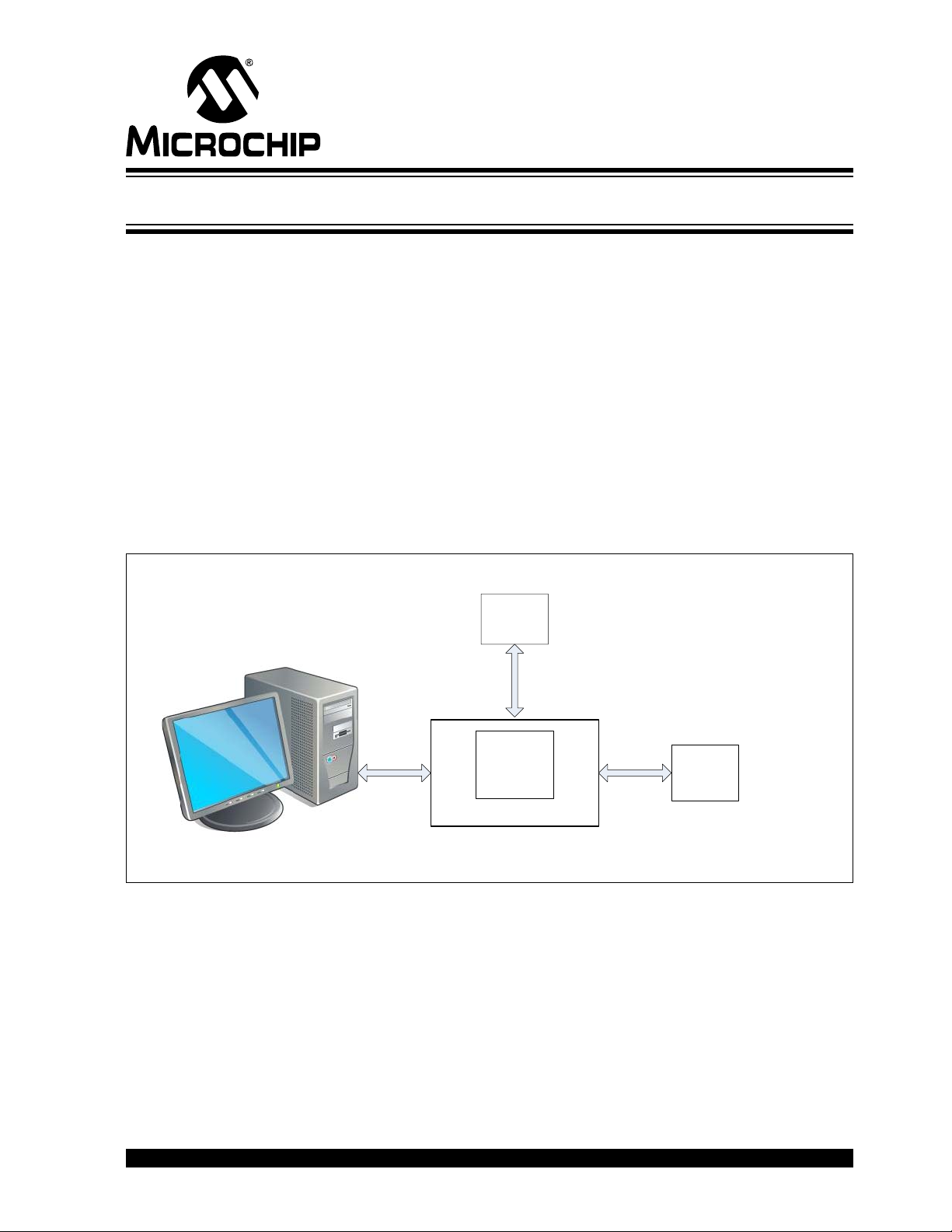
Chapter 1. Product Overview
Portable
Device
PC running UCS81003 GUI
UCS81003
Device
UCS81003 Evaluation Board
OEM USB
Charging Cable
V
S
Cable
USB Cable
1.1 INTRODUCTION
This document provides a description of the software and hardware used to evaluate
the features of the UCS81003.
1.2 UCS81003 EVALUATION SYSTEM
The evaluation system has several components, as shown in Figure 1-1:
• Customer-provided Windows
• UCS81003 graphical user interface (GUI) program
• UCS81003 Evaluation Board
• USB Cable for GUI communications (Standard-A plug to mini-B plug)
• 5V power source (V
• Customer-provided portable device and OEM USB charging cable
(with Standard-A plug at board’s end)
)
S
®
UCS81003 EVALUATION
BOARD USER’S GUIDE
PC
FIGURE 1-1: UCS81003 Evaluation System.
2014 Microchip Technology Inc. DS50002300A-page 11
Page 12
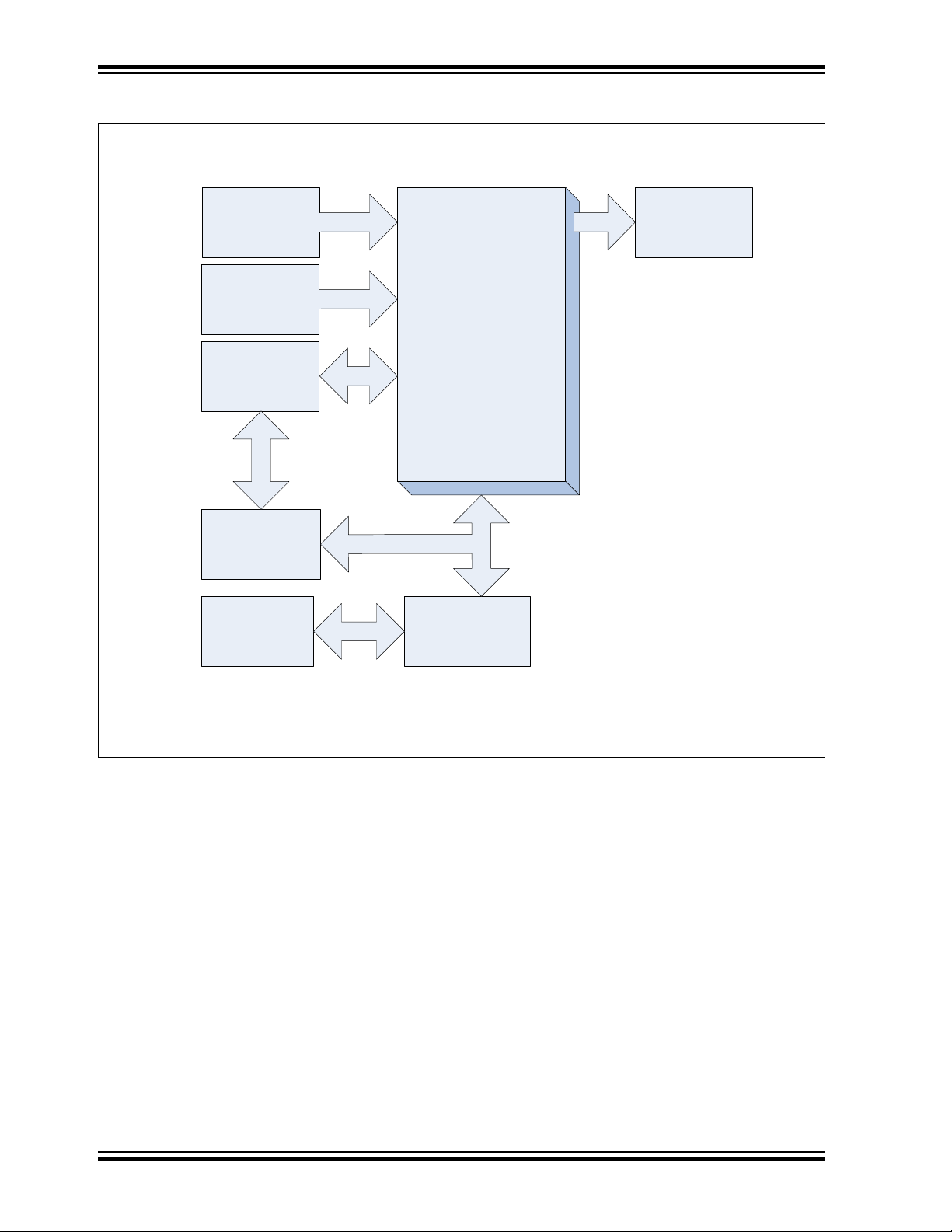
UCS81003 Evaluation Board User’s Guide
USB STD-A PLUG
(Data & Power
From Host)
AUX Input (Power)
UCS81003
USB STD-A
RECPT
(To Portable
Device)
USB Bridge
MCP2221
USB MINI-B
RECPT
Control/Status
Manual/Bridge
Configuration &
Status
A block diagram of the UCS81003 Evaluation Board is shown in Figure 1-2 below:
FIGURE 1-2: UCS81003 Evaluation Board Block Diagram.
1.3 WHAT THE UCS81003 EVALUATION BOARD KIT CONTAINS
This UCS81003 Evaluation Board kit includes:
• UCS81003 Evaluation Board (ADM00561)
• Important Information Sheet
• 5V AC-DC Wall Adapter
• Standard-A plug to mini-B plug USB Cable
DS50002300A-page 12 2014 Microchip Technology Inc.
Page 13
UCS81003 EVALUATION
J2
USB Mini-B
receptacle
to PC
J10
USB Standard-A receptacle
to portable device
J3
USB Stanadrd-A plug to
USB host / USB Power
J1
Auxiliary power connector
to external power supply
BOARD USER’S GUIDE
Chapter 2. Installation and Operation
2.1 INTRODUCTION
This chapter identifies the main connectors, LEDs, jumpers and test points that can be
found on the UCS81003 Evaluation Board. It also explains the steps to install the
board’s graphical user interface.
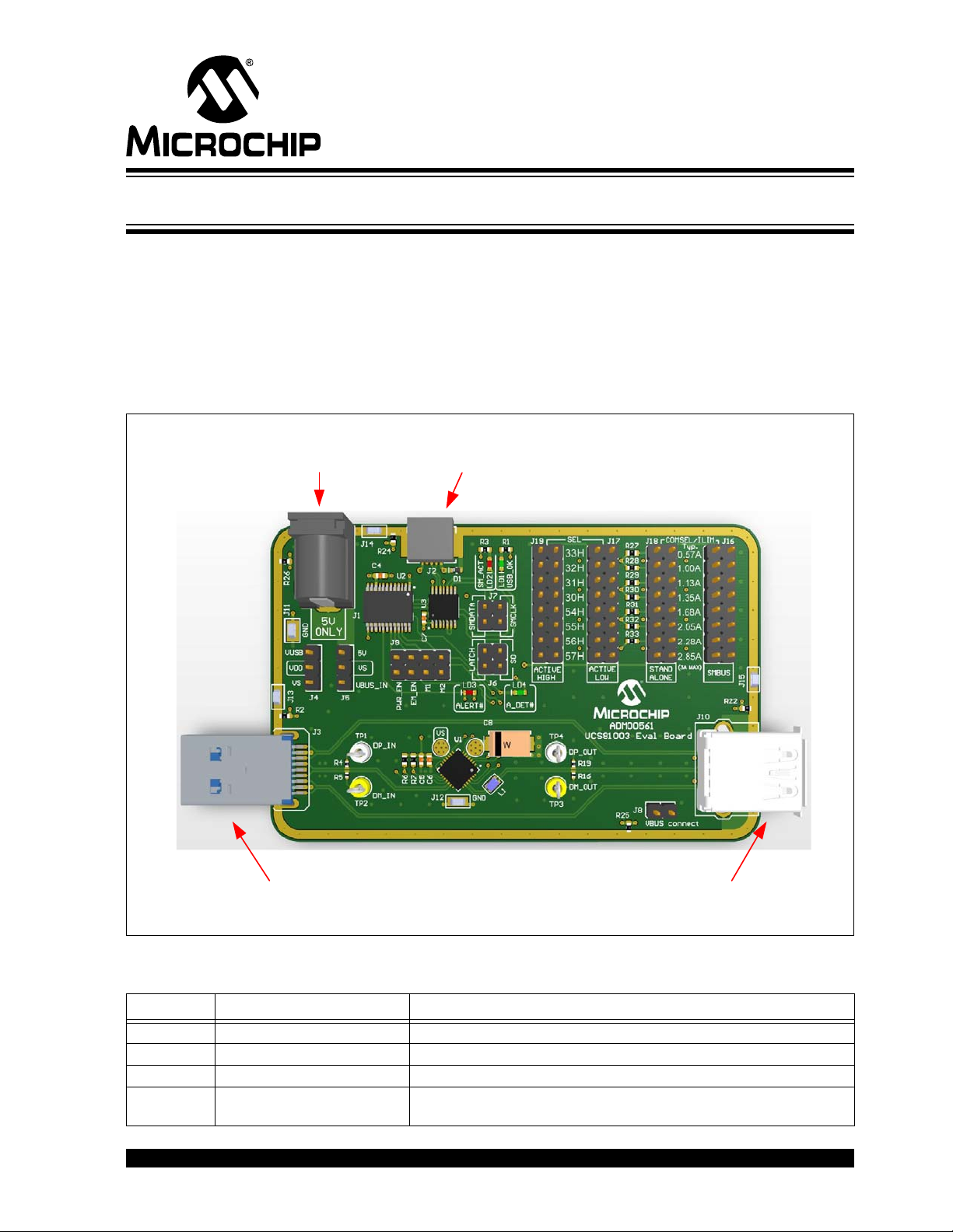
2.2 CONNECTORS ON THE EVALUATION BOARD
Figure 2-1 shows the top of the evaluation board and highlights the connectors.
FIGURE 2-1: UCS81003 Evaluation Board Top View – Connectors.
TABLE 2-1: CONNECTOR DESCRIPTIONS
Designator Connector Type Description
J1 Power jack External 5V power supply
J2 USB Mini-B receptacle This connects the board to the PC with the GUI software
J3 USB Standard-A plug This connects the evaluation board to the USB host
J10 Right-Angle USB Standard-A
receptacle
This connects the board to the portable device
2014 Microchip Technology Inc. DS50002300A-page 13
Page 14
UCS81003 Evaluation Board User’s Guide
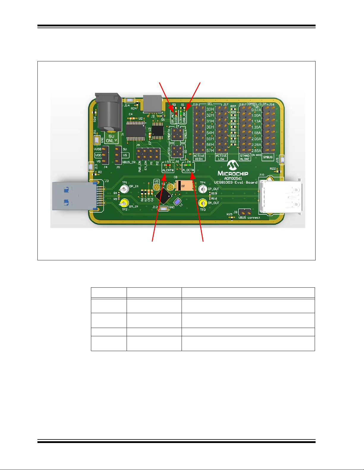
LED4
Attach Detection (green)
LED1
USB_OK
(green)
LED3 ALERT
(red)
LED2
SMBus Activity
(red)
2.3 LEDS ON THE EVALUATION BOARD
Figure 2-2 shows the top of the Evaluation Board and highlights the LEDs.
FIGURE 2-2: Evaluation Board Top View – LEDs.
TABLE 2-2: LED DESCRIPTIONS
Designator Function Description
LD1 USB OK When lit, this green LED means the MCP2221 USB
LD2 SMBus Activity When flashing, this green LED indicates SMBus
LD3 ALERT# When lit, this red LED indicates an alert signal is active.
LD4 A_DET# When lit, this green LED indicates a device is attached
bridge is connected to the PC.
communication activity.
for the UCS81003.
DS50002300A-page 14 2014 Microchip Technology Inc.
Page 15
Installation and Operation
J16
Current Limit,
SMBus mode
J18
Current Limit,
Stand-Alone mode
J8
Connects
UCS81003 V
BUS
output to J10
J9
PWR_EN,
EM_EN,
M1, M2
J17
Address Selection,
PWR_EN Active Low
J19
Address Selection,
PWR_EN Active High
J6
LATCH,
S0
J7
SMBus
data,
clock
J5
V
S
source
selection:
5V from J1 or
from J3 V
BUS
J4
VDD source
selection:
Vs or
V
BUS
from J2
J1
J2
J3 J10
2.4 JUMPERS ON THE EVALUATION BOARD
Figure 2-3 shows the top of the Evaluation Board and highlights the jumpers.
FIGURE 2-3: Evaluation Board Top View – Jumpers.
TABLE 2-3: JUMPER DESCRIPTIONS
Designator Function
J4 V
source selection The jumper populated on this header selects the VDD
DD
Jumper
Position
1-2 V
2-3 V
supply source for the digital circuits on the board.
is connected to V
DD
is connected to VS. This is the recommended
DD
configuration when evaluating the Attach Detection feature
of the UCS81003. If the board is evaluated with a PC
running the GUI, then the V
USB cable is plugged into the J2 connector.
BUS
Description
pin of the J2 USB connector
must be supplied after the
S
2014 Microchip Technology Inc. DS50002300A-page 15
Page 16
UCS81003 Evaluation Board User’s Guide
TABLE 2-3: JUMPER DESCRIPTIONS (CONTINUED)
Designator Function
J5 VS source selection The jumper populated on this header selects the voltage
J6 LATCH, S0
Logic Inputs settings
J7 SMBus data and clock lines If the UCS81003 is in SMBus mode (as selected by using
J8 V
output connection This jumper connects the 5V pin of connector J10 to the
BUS
J9 PWR_EN, EM_EN, M1, M2
Logic Inputs settings
J16 Current Limit
SMBus mode
J18 Current Limit
Stand-alone mode
J17 SMBus Address
PWR_EN active low
Jumper
Position
Description
input source for the power switch inside the UCS81003.
1-2 V
source is the J1 power connector (external 5V power
S
supply).
2-3 V
is connected to V
S
of the J3 USB connector. Use this
BUS
configuration only if the USB host can deliver the necessary
current for charging.
The jumpers must be left off for SMBus communication to
be enabled.
If the UCS81003 is in Stand-Alone mode (as selected by
using J18 instead of J16), then the header pins have the
following functions:
1-2 Jumper placed S0=Logic Low - Detect Power state disabled
No jumper S0=Logic High - Detect Power state enabled
3-4 Jumper placed LATCH=Logic Low - “Auto-retry” fault
handler enabled
No jumper LATCH=Logic High - “Latch” fault handler
enabled
J16 instead of J18), then two jumpers must be populated in
1-2 and 3-4 positions to connect the clock and data lines to
the MCP2221 USB bridge.
The jumpers must be left off if UCS81003 is in Stand-alone
mode.
UCS81003 V
power output pins. A current probe or a
BUS
multimeter can be connected to this header for measuring
the charging current and the voltage, close to the USB
connector.
When a jumper is installed, the corresponding UCS81003
input pin will be in Logic Low state. Otherwise, the
corresponding pin will be in Logic High state.
1-2 PWR_EN
3-4 EM_EN
5-6 M1
7-8 M2
Placing one jumper on this header selects the current limit
and sets the UCS81003 in SMBus mode. In this case, no
jumper must be populated on J18 header.
Placing one jumper on this header selects the current limit
and sets the UCS81003 in Stand-alone mode. In this case,
no jumper must be populated on J16 header.
Placing one jumper on this header selects the SMBus
address and sets the PWR_EN control to be active low. In
this case, no jumper must be populated on J19 header.
DS50002300A-page 16 2014 Microchip Technology Inc.
Page 17

Installation and Operation
TP1
DP_IN
TP3
DM_OUT
TP2
DM_IN
TP4
DP_OUT
TABLE 2-3: JUMPER DESCRIPTIONS (CONTINUED)
Designator Function
J19 SMBus Address
PWR_EN active high
Note: The following headers must be populated with one jumper for the UCS81003
Evaluation Board to be functional:
• J4, J5, J8
• J16 or J18
• J17 or J19
• If
UCS81003 is configured in SMBus mode (as selected by using J16 instead of J18), two
jumpers must be populated on J7 and J6 must be left unpopulated.
configured in Stand-Alone mode, the jumpers on J7 must be left off.
2.5 DATA TEST PO INTS ON THE EVALUATION BOARD
Figure 2-4 shows the top of the board and highlights the USB data line test points.
Jumper
Position
Placing one jumper on this header selects the SMBus
address and sets the PWR_EN control to be active high. In
this case, no jumper must be populated on J17 header.
Description
If UCS81003 is
FIGURE 2-4: Evaluation Board Top View – Data Test Points.
TABLE 2-4:
Designator Assigned Pin Description
TP1 DP_IN This test point connects to the D
TP2 DM_IN This test point connects to the D
TP3 DM_OUT This test point connects to the D
TP4 DP_OUT This test point connects to the D
2014 Microchip Technology Inc. DS50002300A-page 17
data line through a 1 MΩ series resistor.
PIN
data line through a 1 MΩ series resistor.
MIN
data line through a 1 MΩ series resistor.
MOUT
data line through a 1 MΩ series resistor.
POUT
Page 18

UCS81003 Evaluation Board User’s Guide
Signal
Ground
Signal
Ground
Earth
Ground
Earth
Ground
Earth
Ground
2.6 GROUND TEST POINTS ON THE EVALUATION BOARD
Figure 2-5 shows the top of the board and highlights the ground test points.
FIGURE 2-5: Evaluation Board Top View – Ground Test Points.
TABLE 2-5:
Designator Test Point Type Description
J11, J12 Signal Ground These test points connect to the signal ground of the board.
J13, J14, J15 Earth Ground These test points connect to the earth ground of the board (the
These are the ground reference for the UCS81003.
shield of the USB connectors).
DS50002300A-page 18 2014 Microchip Technology Inc.
Page 19

2.7 SOFTWARE INSTALLATION
To begin using the UCS81003 Evaluation Board, software must be installed on a
Windows
1. Download the software archive from the board’s web page, unzip it and
®
-based computer with a USB port.
double-click the Setup.exe, to start the installation. Figure 2-6 shows the initial
installation screen, which displays briefly as the setup program loads.
Installation and Operation
FIGURE 2-6: Software Installation – Initialize Window.
2. Click
Next
in the Destination Directory window, as shown in
operation, the files must be installed in the default locations. The default location
for the software files is
while for the LabVIEW software is
Instruments
.
C:\Program Files(x86)\Microchip\UCS81003\
C:\Program Files(x86)\National
Figure 2-7
. For proper
,
FIGURE 2-7: Software Installation – Setting the Destination Directory.
2014 Microchip Technology Inc. DS50002300A-page 19
Page 20

UCS81003 Evaluation Board User’s Guide
3. Read and accept the license agreement, then click Next.
FIGURE 2-8: Software Installation – Software License Agreement.
4. To use the LabVIEW software, read and accept the license agreement, then click
Next.
FIGURE 2-9: Software Installation – LabVIEW License Agreement.
On the following screens, select Next and follow the on-screen instructions to complete
the installation. When installation is complete, the program will automatically run. If a
screen appears requiring a restart for the changes to take effect, reboot the computer.
The UCS81003 interface will start with the SMBus communications.
DS50002300A-page 20 2014 Microchip Technology Inc.
Page 21

Chapter 3. Hardware Description
3.1 UCS81003 DEVICE
The UCS81003 provides a single USB port power switch for precise control of up to
3.0A continuous current (2.85A typical) with overcurrent limiting, dynamic thermal
management, latch/auto-recovery upon fault, selectable active low or high enable,
under and overvoltage lockout, and back-drive protection.
USB Charging Port profiles are integrated into the UCS81003 to assure compliance to
multiple standards. In addition to power switching and USB Charging Port profiling, the
UCS81003 provides automatic and configurable USB data line handshaking to enable
charging of USB-IF Battery Charging 1.2 (CDP or DCP modes), Chinese
Telecommunications Industry Standard YD/T 1591-2009, Apple
other mobile devices.
The UCS81003 provides a device attachment detection output, as well as a dedicated
alert output, with current monitoring, charge rationing for controlled delivery of current
regardless of a host’s power state. When the limit is reached, the UCS81003 will
perform the user-programmed behavior (report and disconnect is the default).
UCS81003 EVALUATION
BOARD USER’S GUIDE
®
Inc., RIM® and many
3.2 EVALUATION BOARD POWER SOURCE
The UCS81003 has split power supply support:
is the voltage input to Power Switch. This supply rail is required to charge the
•V
S
portable device. V
follows:
Jumper
Position
1-2 VS is supplied from the external 5V power supply connected to J1 power jack.
2-3 V
is the power supply for chip functionality. The UCS81003 Evaluation Board
•V
DD
contains two additional ICs, MCP2221 USB bridge and MCP23018 I/O expander,
which are also powered from the V
populating a jumper on the J4 header, as follows:
Jumper
Position
1-2 V
2-3 V
source is selected by populating a jumper on J5 header, as
S
is supplied from the V
S
only if the USB host port can supply the charging current for the portable
device.
DD
is supplied from V
DD
board in this configuration and the Attach Detection feature of the UCS81003
is used, the V
data sheet.
is connected to VS. This configuration is recommended when using the
DD
Attach Detection feature. If the board is evaluated with a PC running the GUI,
then the V
connector.
voltage must not exceed VDD + 150 mV, as specified in the
S
must be supplied after the USB cable is plugged into the J2
S
BUS
Definition
pin of the J3 USB connector. Use this option
BUS
supply rail. VDD source is selected by
Definition
pin of the J2 USB connector. When using the
2014 Microchip Technology Inc. DS50002300A-page 21
Page 22

UCS81003 Evaluation Board User’s Guide
USB bridge
SCL pin
SMCLK/S0
UCS81003 pin
USB bridge
SDA pin
SMDATA/LATCH
UCS81003 pin
Ground
3.3 MCP2221 USB-TO-SMBUS BRIDGE
The MCP2221 is a USB-to-UART/I2C bridge that supports SMBus communication. It is
controlled through USB interface by the GUI running on the PC. It is the master device
on the SMBus/I2C bus. It is used to read and write the registers of the two devices
connected to the SMBus/I
3.4 MCP23018 I/O EXPANDER
MCP23018 is a 16-bit I/O Expander with open-drain outputs and I2C interface. Its I2C
address is configured to 0100_000(R/W), different than all possible addresses of the
UCS81003.
The I/O pins used in this application are configured as inputs. They are used to read
the logic state of the following UCS81003 pins: ALERT#, ADET#, PWR_EN, EM_EN,
M1, M2.
3.5 DIRECT SMBUS CONNECT OPTION
It is also possible to connect an external SMBus master to the UCS81003 Evaluation
Board. Remove the jumpers on J7 and connect the SMBus master to the header pins
that are linked directly to UCS81003 pins SMDATA/LATCH and SMCLK/S0. Note that
ground must be connected to one of the test point grounds or header pins on the EVB.
See Figure 3-1 for header pins description.
2
C interface: UCS81003 and MCP23018 I/O expander.
DS50002300A-page 22 2014 Microchip Technology Inc.
FIGURE 3-1: UCS81003-to-SMBus Bridge Jumpers.
Page 23

4.1 OVERVIEW
Ta bs
Fixed Panel
with Controls
To get the graphical interface and the evaluation board running, follow these
instructions:
1. Start the UCS81003 GUI software: from the Windows Start menu, select
2. Connect the USB mini connector end of the cable to the board and the standard
The UCS81003 Evaluation Board interface (Figure 4-1), consists of five tabs (Main,
Configuration & General Status , Custom Charging, Register Set and Demo) as
well as the right side sections that are always visible (Panel Controls, Pi n State &
Attach Status and Active Mode Selection).
UCS81003 EVALUATION
BOARD USER’S GUIDE
Chapter 4. Software Description
Programs >
USB connector of the cable to any available USB port on the PC. If the V
supply is connected to VS (the jumper on J4 header is populated on position 2-3),
then connect the VS supply. The USB Activity LED should light, indicating that
the MCP2221 USB bridge is connected to the PC.
Microchip > UCS81003.
DD
FIGURE 4-1: UCS81003 Evaluation Board Initial Window.
2014 Microchip Technology Inc. DS50002300A-page 23
Page 24

UCS81003 Evaluation Board User’s Guide
4.1.1 Tips for Using the EVB GUI
• For many controls on the GUI panel, placing the mouse cursor over a control will
pop up context help that indicates the register address or provides a description.
• After a power up of the evaluation board, the default settings are loaded. Users
can save setting configurations to user-named files which can be reloaded at any
time for quick reconfiguration (see Section 4.3.4.3 “Configuration Save and
Load”).
• The GUI cannot be used to demonstrate UCS81003 behavior in Stand-Alone
mode since SMBus communication is required.
4.1.2 GUI Abbreviations
Abbreviation Description
BC Battery charging
CDP Charging downstream port
DCE Dedicated charger emulation
DCP Dedicated charging port
EM Emulation
EM_EN Emulation enable
M1 Mode control pin number one
M2 Mode control pin number two
4.1.3 Keyboard Shortcuts
Some GUI controls have keyboard shortcuts, as shown in Table 4-1.
TABLE 4-1: UCS81003 EVALUATION BOARD GUI KEYBOARD SHORTCUTS
GUI Control Shortcut Control Description
Run CTRL + R Section 4.2.1.1 “Stop and Run Buttons”
Stop F12 Section 4.2.1.1 “Stop and Run Buttons”
DS50002300A-page 24 2014 Microchip Technology Inc.
Page 25

4.2 INTERFACE DESCRIPTION AND OPERATION
Register Read
Single Read
Stop
Button
COM Status
Single/
Continuous Read
Mode Switch
Delay Button and Field
Indicator
Enable Check Box
Default
Button
Step
Button
Demo
Button
Run Button
Abort Execution
Button
Extended Menu
4.2.1 Panel Controls
The Panel Controls section on the right side of the GUI, shown in Figure 4-2, affects
GUI operation. This section is always displayed.
Software Description
FIGURE 4-2: Panel Controls.
4.2.1.1 STOP AND RUN BUTTONS
Pressing the Stop button, shown in Figure 4-2, interrupts GUI software communication
with the evaluation board. When this button is clicked, the Run button appears under
an extended menu bar, as shown in Figure 4-3.
FIGURE 4-3: Stop and Run Button.
2014 Microchip Technology Inc. DS50002300A-page 25
Page 26

UCS81003 Evaluation Board User’s Guide
4.2.1.2 RUN BUTTON
To restart communication between the software and the evaluation board, click the Run
button. This button disappears when communication resumes.
Note: Stopping and restarting the GUI does not affect register settings. To restore
default register settings, disconnect power from the board, then reconnect
power.
To close the program, press the Close (X) button on the upper right corner of the
window.
4.2.1.3 COM STATUS INDICATOR
The COM Status indicator shows the status of communications over the SMBus.
During normal operation, COM Status is green. If SMBus communications fails, COM
Status turns red (or alternates red and green).
4.2.1.4 REGISTER READ DELAY
The Register Read Delay sets the GUI control panel update speed. It affects the
speed that the software reads the registers, but will not affect the device’s sampling
time. The default is 25 ms. This number can range from 0 to 5000 ms in increments of
25 ms.
4.2.1.5 SINGLE/CONTINUOUS READ
The panel defaults to continuous register reads (toggle switch in down position, as
shown in Figure 4-2). To stop continuous register reads, check the “Single Read
Enable” box. In order to capture the register values at a given time, click the switch,
which will briefly flip to Single Read.
4.2.1.6 DEFAULT
When this button is pressed, it loads the defaults to all registers of the UCS81003.
4.2.1.7 STEP
When selected, Step will go through the Emulation Profiles in sequence, from Legacy 1
through 7, then BC1.2 DCP, and finally Custom. The actual DCE cycle is slightly
different, please see product’s data sheet for more information.
4.2.1.8 DEMO
The Demo button enables an automated routine to cycle through a user-defined set of
profiles and selects the highest current profile. This feature emulates an external
controller and is not part of the UCS81003 device.
DS50002300A-page 26 2014 Microchip Technology Inc.
Page 27

Software Description
ALERT#
Pin
Indicators
A_DET#
Pin Override
Check Boxes
and
Indicators
4.2.2 Pin State and Attach Status Panel
The Pin State & Attach Status section on the right side of the GUI, shown in Figure 4-4,
provides a quick graphical status reference and allows physical control pin override.
This section is always displayed.
FIGURE 4-4: Pin State and Attach Status.
4.2.3 Pin State & Attach Status Panel
4.2.3.1 ALERT# AND A_DET# INDICATORS
When the ALERT# and A_DET# indicators are green, the signals at the device’s
respective pin are low and the corresponding condition has occurred (alert or device
attached, respectively). When the indicators are dark, the pin states are high.
4.2.3.2 PIN INDICATORS
The pin indicators (SEL, PWR_EN, M1, M2 and EM_EN) shown in Figure 4-4 are
green if the signal on the corresponding pin on the UCS81003 device is high, and dark
if the signal is low. If the “Pin Ignore” box is checked (see Section 4.2.3.3 “Pin
Override”), these indicators will reflect the GUI overrides for these pins.
4.2.3.3 PIN OVERRIDE
For evaluation convenience, the GUI can override the setting of the following pins on
the UCS81003 device: PWR_EN, M1, M2 and EM_EN. Check the “Pin Ignore” box
(see Figure 4-4) to enable pin override. Then, check in the corresponding pin box to set
the value high.
Note 1: Pin override does not affect the actual signal on the pin. It only affects the
register values.
2: The SEL pin is only read once by the UCS81003 at power up, so there is
no pin override for it. To close the port power switch, the PWR_EN state
must match the SEL state (e.g., SEL = high and PWR_EN = high).
2014 Microchip Technology Inc. DS50002300A-page 27
Page 28

UCS81003 Evaluation Board User’s Guide
4.2.4 Active Mode Selection
The Active Mode Selection section on the right side of the GUI, shown in Figure 4-5,
provides a quick reference regarding operating state based on the values of M1, M2
and EM_EN. This section is always displayed.
FIGURE 4-5: Charger Emulation Selection.
DS50002300A-page 28 2014 Microchip Technology Inc.
Page 29

4.3 TAB DESCRIPTIONS
Ta b
Status Panel
Measured
Current
Status
Right-click Wave Box
for Plot Appearance Settings
Current Status
Instantaneous
Current
Measurement
Screen
Selection
4.3.1 Main Tab
The Main tab (Figure 4-6) shows key parameters related to the port power switch,
including the maximum current limit, the present current limit (always equal to or less
than maximum current limit), and power state (e.g. detect, active, error, etc.). When a
portable device has been successfully attached, the screen shows the power state
change from Detect to Active and shows the various handshakes applied. Once it is
determined that the device is charging, the screen shows which emulation profile was
successful, and the graph shows the charging current. Optionally, the user may monitor
the charge delivered or ration the charge delivered to the attached device.
Software Description
FIGURE 4-6: Main Tab Window Overview.
4.3.1.1 DEDICATED CHARGER EMULATION (DCE) CYCLE
As shipped, the UCS81003 is ready to function as a dedicated charger, which will be
applied when there is an attach detection. To view this behavior, perform the following:
1. Connect V
Evaluation Board”). The VS_LOW indicator on the bottom of the Main Tab must
be dark. If the color is red, the voltage is not high enough to charge a portable
device.
2. Connect a portable device to the board. Use the OEM USB charging cable that
comes with the portable device.
3. The UCS81003 should detect an attachment, switch to the Active Power state,
apply an emulation profile and deliver a charge. Figure 4-7 shows the interface
after charging has started.
2014 Microchip Technology Inc. DS50002300A-page 29
to the evaluation board (see Section 2.4 “Jumpers on the
S
Page 30

UCS81003 Evaluation Board User’s Guide
VS_LOW
Indicator
Power State
Indicator
Charger
Emulation
Profile
Indicator
A_DET#
is asserted
Pin Status
Power State
Indicator Changed
A_DET#
is deasserted
Disconnect
showing
Point
in Plot
Pin Status
FIGURE 4-7: Main Tab - Charging Started.
4. Disconnect the portable device from the board.
The UCS81003 should detect a removal, switch to the Detect power state, and stop
delivering a charge. Figure 4-8 shows the interface after a removal was detected.
FIGURE 4-8: Main Tab - Removal Detected.
DS50002300A-page 30 2014 Microchip Technology Inc.
Page 31

Software Description
Data
Pass-Through
Options
4.3.1.2 CHARGING DOWNSTREAM PORT (CDP)
The CDP charging profile is based on the “USB Battery Charging Specification v1.x”.
When a BC1.x-compliant portable device attachment is detected, the UCS81003 and
the portable device do handshaking based on the standard. If handshaking is
successful, charging occurs up to the set current limit.
To select the CDP port power profile, M1, M2 and EM_EN must all be high. This can
be done by removing the jumpers for these pins (from J9 header) or by using the pin
override in the GUI (see Section 4.2.3.3 “Pin Override”).
4.3.1.3 PASS-THROUGH
Data Pass-Through does not apply any type of charger emulation. When selected, it
closes the USB high-speed data switch and supplies current up to the current limit.
To select Data Pass-Through, M1, M2 and EM_EN can be set to any one of the two
DATA PASS-THRU combinations (010 and 110), as shown in Figure 4-9. This can be
done by setting the jumpers for these pins (from J9 header –
see Section 2.4 “Jumpers on the Evaluation Board”) or by using the pin override in
the GUI (see Section 4.2.3.3 “Pin Override”).
FIGURE 4-9: Data Pass-Through Selection Options.
4.3.1.4 CURRENT MONITORING AND CHARGE RATIONING
To view current monitoring and current rationing, perform the following on the Main tab:
1. Set a Ration Limit. The ration limit is expressed in mAh (electric charge).
2. Set rationing behavior. The Ration Completion Behavior defaults to “Report &
Disconnect”. Once the ration limit is reached, portable device charging will
cease, the ALERT# pin will assert, and the Ration Complete bit will be set. If
you do not want the system to behave in this fashion, select one of the other
three options from the Ration Completion Behavior drop-down list: Report,
Report & Sleep or Take No Action.
3. Connect V
Evaluation Board”). The VS_LOW indicator on the bottom of the Main Tab must
be dark. If the VS_LOW indicator is red, the voltage is not high enough to charge
a portable device.
4. Connect a portable device to the evaluation board. Use the OEM USB charging
cable that comes with the portable device.
5. Enable rationing by checking the Ration Enable check box on the Main Tab.
6. Watch the GUI as the device starts charging. Figure 4-10 shows the interface
after the ration limit was reached (for “Report & Disconnect” behavior setting).
to the evaluation board (see Section 2.4 “Jumpers on the
S
2014 Microchip Technology Inc. DS50002300A-page 31
Page 32

UCS81003 Evaluation Board User’s Guide
Power State
Indicator Changed
Pin is
Instantaneous
Ration Limit
Setting
Rationing
Behavior
ALERT#
Complete
Rationing
Indicator
Ration
Enable
Current (mA)
Delivered
Current
Measured
Current
Status
VS_LOW
Indicator
Charge
(mAh)
Asserted
Note: As shown in Figure 4-10, the green trace is the instantaneous current, while
the red diagonal line is the charge being delivered in mAh. Both are also
presented in numeric format in the bottom left boxes. Trace color and
characteristics can be changed by clicking on the waveform boxes to the
left of these numerical values.
FIGURE 4-10: Main Tab - Ration Limit Reached.
DS50002300A-page 32 2014 Microchip Technology Inc.
Page 33

Software Description
Configuration Tab
Selected
Interrupt and General
Status
Emulation Profile
Disable
Emulation
Behavior Option
Comm.,
Fault
Handler,
Controls
General
and
Thermal
Emulation
Settings
4.3.2 Configuration and General Status Tab
The Configuration & General Status tab (Figure 4-11), includes various status
indicators and configuration controls. Items are grouped by function, detailed in the
following sections.
FIGURE 4-11: Configuration & General Status Tab.
4.3.2.1 INTERRUPT STATUS
The indicators in the Interrupt Status section turn green when the corresponding bit is
high, and are dark when the bit is low.
4.3.2.2 GENERAL STATUS
Indicators in the General Status section turn green when the corresponding bit is high
and are dark when the bit is low.
4.3.2.3 EMULATION BEHAVIOR
Check the necessary check box to enable the corresponding emulation behavior.
4.3.2.4 COMMUNICATIONS
SMBus address is displayed. SMBus timeout can be disabled.
4.3.2.5 EMULATION PROFILE DISABLE
Check the Profiles boxes to disable them. They will not be used during emulation. By
selecting the “Disable ALL” will toggle all profile check boxes.
2014 Microchip Technology Inc. DS50002300A-page 33
Page 34

UCS81003 Evaluation Board User’s Guide
4.3.2.6 ATTACH/REMOVE ENABLE
Click the S0_SET box to remove the check mark and disable the function.
4.3.2.7 FAULT HANDLER
These are controls related to fault handling.
4.3.2.8 GENERAL CONTROL
Controls for general parameters.
4.3.2.9 THERMAL REGULATION
Controls for thermal and detection delay parameters.
4.3.2.10 PORT POWER KEEP-OUT
Displays values for the port power parameters.
4.3.2.11 GENERAL EMULATION/CHARGING SETTINGS
Controls for emulation and charging.
4.3.2.12 EMULATION TIMEOUTS
Sets the emulation timeout period for each profile. These timeout periods are not used
if the EM_TIMEOUT_DIS control in the Emulation Behavior section is checked.
4.3.2.13 CHARGING THRESHOLD CURRENT
Controls charging threshold current setting.
4.3.2.14 HIGH SPEED SWITCH CONFIGURATION
Controls the high-speed switch parameters.
DS50002300A-page 34 2014 Microchip Technology Inc.
Page 35

Software Description
Custom Charging Tab
Selected
Custom Emulation
Configuration Setting
Custom Current
Limiting Behavior
Custom Emulation
Quick Load Selection
Custom Emulation
Save Option
Custom Emulation
Timeout Custom Setting
Selection
4.3.3 Custom Charging Tab
The Custom Charging tab (Figure 4-12), provides the means for users to create
custom charger emulator configurations. These configurations include signaling on the
USB data lines, as well as what method of current limiting to employ (Constant Current
or Trip). For more information, refer to the UCS81003 Data Sheet and AN24.14 -
“UCS1002 Fundamentals of Custom Charger Emulation” (DS200005234).
FIGURE 4-12: Custom Charging Tab.
4.3.3.1 CUSTOM EMULATION CONFIGURATION
Creating a custom emulation profile is a two-part process of entering the appropriate
stimulus-response pairs in the provided fields, as well as the desired current limiting
behavior (after emulation is applied, and the portable device starts to draw current).
4.3.3.1.1 Example
Settings shown in Figure 4-12 will apply the Legacy 2 stimulus pair. This includes a
voltage divider on DP and on DM with the values shown under STEP 5 column.
If the portable device draws bus current greater than the charging threshold being
used, it will always operate in Current Limiting Trip mode (with trip point based on the
current limit setting).
2014 Microchip Technology Inc. DS50002300A-page 35
Page 36

UCS81003 Evaluation Board User’s Guide
Region 2
Drop-down List
Click on the arrow
to reveal the options
in the VBus_Min
Drop-down List
Current Limit
4.3.3.2 CUSTOM CURRENT LIMITING BEHAVIOR
The second part of creating custom profiles is to specify the behavior of current limiting
and minimum voltage output. This is accomplished using the Ibus_r2min and
VBus_Min drop-down lists, as shown in Figure 4-13.
FIGURE 4-13: Current -Voltage Behavior Selectio n.
4.3.3.3 CUSTOM EMULATION QUICK LOAD
The Custom Emulation Quick Load drop-down menu allows single-click loading of the
Custom Emulation Configuration registers. Simply select the profile to load from the
menu and registers 41h – 4Ch will be loaded with that profile.
4.3.3.4 SAVE CUSTOM EMULATION CONFIGURATION
Customs Emulation Configuration allows for a quick way to save the necessary registers to configure the UCS81003 for a custom profile to a file. Enter the path and press
the SAVE button. Files will be overwritten if duplicate file names are used.
Registers 40h – 4Ch (Custom Emulation Configuration - Custom Charging tab),
16h (Emulation Behavior - Configuration tab), 19h (ILIM - Main tab), 25h (High Speed
Switch Configuration – Configuration tab) and 51h (Custom Current Limiting Behavior
– Custom Charging tab) will be saved in a two-column format. Comments can be
added at the end of the file for documentation.
DS50002300A-page 36 2014 Microchip Technology Inc.
Page 37

Software Description
Register Set Tab
Selected
Load/Save Register
Register Content List
Product
Section
Information
4.3.4 Register Set Tab
The Register Set tab (Figure 4-14), allows viewing and updating of the UCS81003
registers, identifies the device on the evaluation board and manages configuration files.
FIGURE 4-14: Register Set Tab.
4.3.4.1 REGISTER CONTENT
Register Content shown in Figure 4-14 is a scrollable list of the UCS81003 registers
and the current value. It is important to note that not all addresses are physical memory
locations on the device; these registers will read ‘0’. Likewise, some registers shown,
that are undocumented in the data sheet, may contain data. Editing these registers can
cause unexpected results.
To update a register value, locate the register address in the left column, type the new
value in the corresponding cell in the right column, and press Enter on the keyboard or
click outside the editable field to complete the action.
4.3.4.2 PRODUCT INFORMATION
Product Information panel shows the values of three registers (FDh, FEh and FFh)
which identify the device on the evaluation board.
4.3.4.3 CONFIGURATION SAVE AND LOAD
The Register Set tab contains controls (Figure 4-15) which save the settings currently
configured in the UCS81003 to allow quick reconfiguration at any time.
2014 Microchip Technology Inc. DS50002300A-page 37
Page 38

UCS81003 Evaluation Board User’s Guide
Browse for Location
Buttons
Path Fields
Load/Save All Register
Values Buttons
FIGURE 4-15: Save/Load Section.
To save configuration settings, configure the UCS81003 as desired, then display the
Register Set tab. Type a path in the “File Stored Path” field or press the Browse button
to select the folder where the configuration file will be saved. The file should be named
with the .txt extension or with a similar text file format. Once a file name and location
has been chosen, click the Save All Register V alues switch, and the file is saved.
Note: If a file with the same name already exists, it will be overwritten and the old
data will be lost.
The data is saved in two columns separated by tabs. The first column is the register
address and the second column is the register data.
Once a file is saved, it can be recalled at any time by selecting the file in the “File Load
Path” field and clicking the Load All Register Values switch.
DS50002300A-page 38 2014 Microchip Technology Inc.
Page 39

Software Description
Demo Tab
Selected
Demo Options
Quick
Step 2
Load
Custom
Panel
Option
Demo
Button
Step 1
Configure Device
Emulation
Config
Options
Demo
Results
4.3.5 Demo Tab
The Demo tab (Figure 4-16) demonstrates external controller logic to apply custom
emulation profiles and optimize charging current. This feature uses the LabView engine
to step through the selected files and store the current drawn by the device. Several
options are available to customize the operation of the demo and explore the potential
of the UCS81003.
FIGURE 4-16: Demo Tab.
4.3.5.1 STEP 1: CONFIGURE DEVICE FOR DEMO ROUTINE
The first step in preparing to run the Demo feature is to configure the device to the
desired starting configuration. A file has been preloaded at installation and is ready to
be used, or a new configuration can be created. Each time the Demo button (in the
Panel Control section) is toggled, the Setup.txt file will be loaded.
4.3.5.2 STEP 2: DEFINE CUSTOM EMULATION CONFIGURATIONS
At installation, a set of files are preloaded on the users system (profile1.txt –
profile7.txt) with the default profiles of the UCS81003. These files can be
changed easily by using the Custom Charging tab.
4.3.5.2.1 Active Files
Check the corresponding check box to activate the desired profile in the demo routine.
4.3.5.2.2 Custom Emulation Files
This column contains the full path to the profile file to be loaded. This file should contain
registers 40h – 4Ch, 16h and 25h. This file can be created with the GUI on the Custom
Charging tab.
2014 Microchip Technology Inc. DS50002300A-page 39
Page 40

UCS81003 Evaluation Board User’s Guide
4.3.5.2.3 Current Reading
This column displays the current being drawn from the attached device. If End Value is
selected (from the Demo Options section, Current Reading features), this will update
continuously. If MAX Value is selected, this will store the highest value of current during
the dwell time.
4.3.5.2.4 Dwell Time
Dwell Time column defines the amount of time from PWR_EN set to PWR_EN unset.
Each profile can have a different Dwell Time.
4.3.5.3 DEMO OPTIONS
TABLE 4-2: DEMO OPTIONS DESCRIPTION
Options Description
Repeat if 0 mA When this option is set, it will repeat if all of the profiles read 0 mA,
i.e. no device connected
Repeat Forever When set, it will repeat the set of files until unchecked
Dead Batt. Repeat When set, it will start the demo after the initial cycle after the
specified Dead Batt. Delay time. This is useful when the battery is
completely discharged and the device OS is unable to handshake
with UCS81003.
Dead Batt. Delay This option is defined in minutes. Minimum is 0 minutes, maximum
is 10 minutes.
Current Reading Displays either the End Value (last value before PWR_EN set low)
or MAX Value (highest value during Dwell Time)
4.3.5.4 CUSTOM FILE PATH QUICK LOAD
When starting the UCS81003 interface, the file paths are reset to a default path. If
desired, the user may save the files in an alternate location. This quick load feature
saves the paths of the Setup.txt and all seven profile locations to quickly return or
change files with one click.
4.3.5.5 RUNNING THE DEMO
Once the files and settings are configured as desired, enable the Demo routine by
pressing the Demo switch within the Panel Controls area. The routine begins and the
results are displayed in Profile MAX and Current MAX. By default, the Demo routine
will enable the profile that is indicated by Profile MAX.
• Profile MAX: Stores the profile of the highest value of current draw.
• Current MAX: Stores the highest current associated with the Profile MAX #.
Note: The Demo tab does not need to be visible to activate the Demo routine.
DS50002300A-page 40 2014 Microchip Technology Inc.
Page 41

Software Description
4.4 TROUBLESHOOTING
Ta bl e 4 - 3 identifies possible problems and their solutions to troubleshoot the
UCS81003 software.
TABLE 4-3: TROUBLESHOOTING THE INTERFACE - COMMON PROBLEMS
Problem Solution
GUI Controls Unresponsive
After Installation
GUI Freezes If the GUI freezes for unknown reasons, communications cannot be stopped, and
Random Panel Display When a board is not connected to the PC running the GUI, the panel will be in an
Device Is Not Charging or Not
Charging Optimally
Restart the computer. In some cases, a restart is required after installation.
the program cannot be closed, disconnect the USB cable from the evaluation
board, then close the program. Reconnect the board, then restart the GUI.
all-zero register displayed state. This also occurs when SMBus communications
are disconnected. The panel display is not meaningful. Connect the board and
establish SMBus communications. If this still does not work, there is a problem
with the connection. The cable or the USB port may be defective.
• Check if the current limit jumper is set appropriately.
• The current source may not have high enough capacity from V
• Run the Demo routine to determine highest current profile.
.
S
2014 Microchip Technology Inc. DS50002300A-page 41
Page 42

UCS81003 Evaluation Board User’s Guide
NOTES:
DS50002300A-page 42 2014 Microchip Technology Inc.
Page 43

Appendix A. Schematic and Layouts
A.1 INTRODUCTION
This appendix contains the following schematics and layouts for the UCS81003
Evaluation Board:
• Board – Schematic
• Board – Top Silk
• Board – Top Copper and Silk
• Board – Top Copper
• Board – Inner Plans GND 1
• Board – Inner Plans GND 2
• Board – Bottom Copper
• Board – Bottom Copper and Silk
• Board – Bottom Silk
UCS81003 EVALUATION
BOARD USER’S GUIDE
2014 Microchip Technology Inc. DS50002300A-page 43
Page 44

2014 Microchip Technology Inc. DS50002300A-page 44
VBUS
G
VDD
0
GP1
UA
GP2
G
SDA
SC
VUS
D
VSS
VSS
NTB
VBUS
SSRX-
+
VBUS
-
A.2 BOARD – SCHEMATIC
SHIELD
J2
VBUS
GND
0
SHIELD
VDD_5V
USB_OK
J1
JACK Power 2.1mm Male
GND
J3
VBUS
GND
SSRX-
SSRX
SSRX+
GND_D
SSTX-
SSTX+
Shield
USB 3.0 A PLUG
0
SHIELD
D1
5V
1
2
D-
3
D+
D+
4
ID
5
ND
USB MINI-B Female
VDD_5V
R1
1k
0603
5%
LD1
GREEN
1
3
2
C1
0603
0.1uF 25V
1
2
D-
D-
3
D+
D+
4
5
SSRX_N
6
SSRX_P
7
GND_DRAIN
8
SSTX_N
9
SSTX_P
R2
0R
0603
VDD_5V
123
USB_N
USB_P
GND
R3
1k
0603
5%
LD2
RED
SM_ACT
5V_IN
GND
VBUS_IN
GND
TP LOOP White
J4
HDR-2.54 Male 1x3
SMDATA/LATCH
SMCLK/S0
J5
123
HDR-2.54 Male 1x3
GND
GND
R4
1M
0402
1%
TP1
DP_IN
VDD_5V
GND
C2
10uF 10V
C3
0.01uF 16V
R5
1M
0402
1%
TP2
TP LOOP Yellow
DM_IN
VS_5V
R6
10k
0603
1%
12
34
J6
HDR-2.54 Male 2x2
VS_5V
0805
0603
D_IN_N
D_IN_P
PWR_EN
EM_EN
M1
M2
VDD_5V
VDD_5V
R8
10k
0603
1%
1
2
GP0
3
GP1
4
RESET
5
RX
6
TX
USB_OK SM_ACT
VDD_5V
R9
R7
10k
0603
J7
1%
HDR-2.54 Male 2x2
R10
2.2k
2.2k
0603
0603
34
1%
1%
12
GND
RESET
VDD_5V
C4
0.1uF
25V
0603
GND
VDD_5V
C5
1uF 16V
C6
0.1uF 25V
U1
12
VDD
9
VS1
10
VS2
11
VS3
20
DMIN
19
DPIN
13
PWR_EN
26
EM_EN
2
M1
3
M2
27
COMM_I_LIM
GND
29
EP
NC
NC14NC
NC21NC
1
GND
15
C7
0.1uF 25V
U3
VDD
GP0
GP
GP1
RST
RST
UART RX
RT RX
UART TX
UART TX
GP27GP3
MCP2221
C11
4.7uF 16V
U2
11
SCL
12
SDA
13
ADDR
14
RESET
16
INTA
15
INTB
10
VDD
1
VSS
MCP23018
0603
0603
GND
4
VBUS1
5
VBUS2
6
VBUS3
23
DMOUT
24
DPOUT
25
A_DET#
18
ALERT#
16
SMDATA
17
SMCLK
7
8
SEL
NC
UCS81003
22
28
0603
0603
VUSB
GPA0
GPA1
GPA2
GPA3
GPA4
GPA5
GPA6
GPA7
GPB0
GPB1
GPB2
GPB3
GPB4
GPB5
GPB6
GPB7
VSS
D+
+
D-
D
B
SCL
L
SDA
P3
VBUS_5V
C8
150uF 10V
D_OUT_N
D_OUT_P
A_DET#
ALERT#
SMDATA/LATCH
SMCLK/S0
COMM_SEL/ILIM
SEL
14
13
12
11
10
9
8
GND
17
18
19
20
21
22
23
24
2
3
4
5
6
7
8
9
SDA
SCL
GND
USB_P
USB_N
VUSB
ALERT#
A_DET#
PWR_EN
EM_EN
M1
M2
TANT-D
L1
CM Choke 90Ohm
VDD_5V
C9
0.47uF 6.3V
GND
L1L1'
L2L2'
LD3
ALERT#
RED
R14
1k
0603
5%
0603
J8
D_OUT_N
D_OUT_P
VDD_5V
GND
VDD_5V
1
2
LD4
A_DET#
GREEN
R18
1k
0603
5%
TP LOOP Yellow
DM_OUT
R27
JP1
Shunt 2.54mm 1x2 Handle11
R17
R20
R21
10k
0603
1%
R23
10k
10k
10k
0603
0603
0603
1%
1%
1%
J9
1 2
3 4
5 6
7 8
HDR-2.54 Male 2x4
GND
GND
47k
R28
56k
R29
68k
R30
82k
R31
100k
R32
120K
R33
150k
R41
0R
R42
10k
R43
12k
R44
15k
R45
18k
R46
22k
R47
27k
R48
33k
VDD_5V
0.57A
1.00A
1.13A
1.35A
1.68A
2.05A
2.28A
2.85A
GND
R34
47k
R35
56k
R36
68k
R37
82k
R38
C10
GND
D4
5V
SOD-882
470pF 50V
SSRX_N
SSRX_P
GND_DRAIN
SSTX_N
SSTX_P
0603
J10
1
VBUS
2
D-
D-
3
D+
D
4
GND
5
6
7
8
9
SSRX-
SSRX+
GND_D
SSTXSSTX+
Shield
SHIELD
J11
GND
J12
GND
USB 3.0 A RCPT
0
J13
1
SHIELD
J14
SHIELD
J15
SHIELD
R24
0R
0603
GND
1
R25
0R
0603
GND
1
R26
0R
0603
GND
SHIELD
1
GND
SHIELD
1
GND
SHIELD
GND
GND
D2
5V
SOD-523
D3
5V
SOD-882
R22
0R
0603
GND
VBUS_OUT
GND
R19
R16
1M
1M
0402
0402
1%
1%
TP3
TP4
TP LOOP White
DP_OUT
100k
R39
120K
R40
150k
R49
0R
R50
10k
R51
12k
R52
15k
R53
18k
R54
22k
R55
27k
R56
33k
VDD_5V
AL_57h
AL_56h
AL_55h
AL_54h
AL_30h
AL_31h
AL_32h
AL_33h
0.57A_SA
1.00A_SA
1.13A_SA
1.35A_SA
1.68A_SA
2.05A_SA
2.28A_SA
2.85A_SA
J16
1
2
3
4
5
6
7
8
9
10
12
11
14
13
16
15
HDR-2.54 Male 2x8
AH_33h
AH_32h
AH_31h
AH_30h
AH_54h
AH_55h
AH_56h
AH_57h
J17
15
16
13
14
11
12
9
10
8
7
6
5
4
3
2
1
HDR-2.54 Male 2x8
J18
COMM_SEL/ILIM
1
2
3
4
5
6
7
8
9
10
12
11
14
13
16
15
HDR-2.54 Male 2x8
COMM_SEL/ILIM
J19
1
2
3
4
5
6
7
8
9
10
12
11
14
13
16
15
HDR-2.54 Male 2x8
SEL
SEL
Schematic and Layouts
Page 45

A.3 BOARD – TOP SILK
Schematic and Layouts
A.4 BOARD – TOP COPPER AND SILK
2014 Microchip Technology Inc. DS50002300A-page 45
Page 46

UCS81003 Evaluation Board User’s Guide
A.5 BOARD – TOP COPPER
A.6 BOARD – INNER PLANS GND 1
DS50002300A-page 46 2014 Microchip Technology Inc.
Page 47

A.7 BOARD – INNER PLANS GND 2
Schematic and Layouts
A.8 BOARD – BOTTOM COPPER
2014 Microchip Technology Inc. DS50002300A-page 47
Page 48

UCS81003 Evaluation Board User’s Guide
A.9 BOARD – BOTTOM COPPER AND SILK
A.10 BOARD – BOTTOM SILK
DS50002300A-page 48 2014 Microchip Technology Inc.
Page 49

UCS81003 EVALUATION
BOARD USER’S GUIDE
Appendix B. Bill of Mater ials
TABLE B-1: BILL OF MATERIALS (BOM)
Qty. Reference Description Manufacturer Part Number
4 C1, C4, C6, C7 Cap. ceramic 0.1 μF 25V 10% X7R
SMD 0603
1 C2 Cap. ceramic 10 μF 10V 10% X7R
SMD 0805
1 C3 Cap. ceramic 0.01 μF 16V 10% X7R
SMD 0603
1 C5 Cap. ceramic 1 μF 16V 10% X7R SMD
0603
1 C8 Cap. tantalum 150 μF 10V 10% 100m
ohm SMD D
1 C9 Cap. ceramic 0.47 μF 6.3V 10% X5R
SMD 0603
1 C10 Cap. ceramic 470 pF 50V 10% X7R
0603
1 C11 Cap. ceramic 4.7 uF 16V 10% X5R
SMD 0603
2 D1, D2 Diode Zener T5V0S5-7 5V 150 mW
SMD SOD-523
2 D3, D4 Diode Zener PESD5V0X1BL 5V SMD
SOD-882
1 J1 Conn. jack power 2.1 mm 16V 2.5A
male th. R/A
11 JP1 Mech. hardware jumper 2.54 mm 1x2
handle gold
1 J2 Conn. USB Mini-B female SMD R/A Hirose Electric Co., Ltd. UX60SC-MB-5ST(80)
1 J3 Conn. USB 3.0 Standard-A plug SMD
R/A
2 J4, J5 Conn. header-2.54 male 1x3 gold
5.84 MH th. vert.
1 J6 Conn. header-2.54 male 2x2 gold
5.84MH th. vert.
1 J7 Conn. header-2.54 male 2x2 gold
5.84MH th. vert.
1 J8 Conn. header-2.54 male 1x2 gold
5.84MH th. vert.
1 J9 Conn. header-2.54 male 2x4 gold
5.84MH th. vert.
1 J10 Conn. USB 3.0 Standard-A rcpt. th. R/A Wurth Elektronik GmbH &
5 J11, J12, J13, J14,
J15
Note 1: The components listed in this Bill of Materials are representative of the PCB assembly. The released BOM
used in manufacturing uses all RoHS-compliant components.
Conn. TP loop tin SMD FCI 68602-116HLF
Murata Electronics
Murata Electronics GRM21BR71A106KE51L
Samsung Group CL10B103KO8NNNC
Taiyo Yuden Co., Ltd. EMK107B7105KA-T
AVX Corporation TPSD157K010R0100
Murata Electronics GRM188R60J474KA01D
TDK Corporation C1608X7R1H471K
TDK Corporation C1608X5R1C475K080AC
®
Diodes
NXP Semiconductor PESD5V0X1BL,315
CUI Inc. PJ-002A
TE Connectivity, Ltd. 881545-2
Wurth Elektronik GmbH &
Co.
FCI 68000-103HLF
Samtec, Inc. TSW-102-07-G-D
Samtec, Inc. HTSW-102-07-G-D
FCI 68001-202HLF
Samtec, Inc. TSW-104-08-L-D
Co.
Incorporated T5V0S5-7
®
GRM188R71E104KA01D
692112030100
692121030100
2014 Microchip Technology Inc. DS50002300A-page 49
Page 50

UCS81003 Evaluation Board User’s Guide
TABLE B-1: BILL OF MATERIALS (BOM) (CONTINUED)
Qty. Reference Description Manufacturer Part Number
4 J16, J17, J18, J19 Conn. header-2.54 male 2x8 gold
5.84MH th. vert.
1 L1 Inductor choke Common Mode 90 ohm
0805
2 LD1, LD4 Diode LED green 2.2V 25mA 15 mcd
clear SMD 0603
2 LD2, LD3 Diode LED red 1.95V 30 mA 700 mcd
clear SMD 0603
4 R1, R3, R14, R18 Res. TKF 1k 5% 1/10W SMD 0603 Panasonic
7 R2, R22, R24, R25,
R26, R41, R49
4 R4, R5, R16, R19 Res. TKF 1M 1% 1/10W SMD 0402 Panasonic ERJ-2RKF1004X
9 R6, R7, R8, R17,
R20, R21, R23,
R42, R50
2 R9, R10 Res. TKF 2.2k 1% 1/10W SMD 0603 Panasonic ERJ-3EKF2201V
2 R27, R34 Res. TKF 47k 1% 1/10W SMD 0603 Panasonic ERJ-3EKF4702V
2 R28, R35 Res. TKF 56k 1% 1/10W SMD 0603 Stackpole Electronics, Inc. RMCF0603FT56K0
2 R29, R36 Res. TKF 68k 1% 1/10W SMD 0603 Stackpole Electronics, Inc. RMCF0603FT68K0
2 R30, R37 Res. 82K ohm 1/10W 1% 0603 SMD Panasonic ERJ-3EKF8202V
2 R31, R38 Res. TKF 100k 1% 1/10W SMD 0603 Panasonic ERJ-3EKF1003V
2 R32, R39 Res. TKF 120K 1% 1/10W SMD 0603 Panasonic ERJ-3EKF1203V
2 R33, R40 Res. TKF 150k 1% 1/10W SMD 0603 Panasonic ERJ-3EKF1503V
2 R43, R51 Res. TKF 12k 1% 1/10W SMD 0603 Yageo Corporation RC0603FR-0712KL
2 R44, R52 Res. TKF 15k 1% 1/10W SMD 0603 Panasonic ERJ-3EKF1502V
2 R45, R53 Res. TKF 18k 1% 1/10W SMD 0603 ROHM Semiconductor MCR03EZPFX1802
2 R46, R54 Res. TKF 22k 1% 1/10W SMD 0603 Stackpole Electronics, Inc. RMCF0603JT22K0
2 R47, R55 Res. TKF 27k 1% 1/10W SMD 0603 Yageo Corporation RC0603FR-0727KL
2 R48, R56 Res. TKF 33k 1% 1/10W SMD 0603 Stackpole Electronics. Inc. RMCF0603FT33K0
2 TP1, TP4 Conn. TP loop white th. Keystone Electronics
2 TP2, TP3 Conn. TP loop yellow th. Keystone Electronics
1 U1 UCS81003 QFN-28_5X5_EP2.7x3 Microchip Technology Inc. UCS81003AM-C1A
1 U2 Microchip interface GPIO-port Expand.
1 U3 MCP2221 TSSOP-14 Microchip Technology Inc. MCP2221- I/ST
Note 1: The components listed in this Bill of Materials are representative of the PCB assembly. The released BOM
used in manufacturing uses all RoHS-compliant components.
Res. TKF 0R 1/10W SMD 0603 NIC Components Corp. NRC06Z0TRF
Res. TKF 10k 1% 1/10W SMD 0603 NIC Components Corp. NRC06F1002TRF
I2C 16-port MCP23018-E/SS SSOP-24
FCI 68602-116HLF
Murata Electronics DLW21HN900SQ2L
Kingbright Corp. APT1608SGC
Kingbright Corp. APTD1608SURCK
®
Corp.
Corp.
Microchip Technology Inc. MCP23018-E/SS
ERJ-3GEYJ102V
5012
5014
DS50002300A-page 50 2014 Microchip Technology Inc.
Page 51

NOTES:
Bill of Materials
2014 Microchip Technology Inc. DS50002300A-page 51
Page 52

Worldwide Sales and Service
AMERICAS
Corporate Office
2355 West Chandler Blvd.
Chandler, AZ 85224-6199
Tel: 480-792-7200
Fax: 480-792-7277
Technical Support:
http://www.microchip.com/
support
Web Address:
www.microchip.com
Atlanta
Duluth, GA
Tel: 678-957-9614
Fax: 678-957-1455
Austin, TX
Tel: 512-257-3370
Boston
Westborough, MA
Tel: 774-760-0087
Fax: 774-760-0088
Chicago
Itasca, IL
Tel: 630-285-0071
Fax: 630-285-0075
Cleveland
Independence, OH
Tel: 216-447-0464
Fax: 216-447-0643
Dallas
Addison, TX
Tel: 972-818-7423
Fax: 972-818-2924
Detroit
Novi, MI
Tel: 248-848-4000
Houston, TX
Tel: 281-894-5983
Indianapolis
Noblesville, IN
Tel: 317-773-8323
Fax: 317-773-5453
Los Angeles
Mission Viejo, CA
Tel: 949-462-9523
Fax: 949-462-9608
New Yor k , NY
Tel: 631-435-6000
San Jose, CA
Tel: 408-735-9110
Canada - Toronto
Tel: 905-673-0699
Fax: 905-673-6509
ASIA/PACIFIC
Asia Pacific Office
Suites 3707-14, 37th Floor
Tower 6, The Gateway
Harbour City, Kowloon
Hong Kong
Tel: 852-2943-5100
Fax: 852-2401-3431
Australia - Sydney
Tel: 61-2-9868-6733
Fax: 61-2-9868-6755
China - Beijing
Tel: 86-10-8569-7000
Fax: 86-10-8528-2104
China - Chengdu
Tel: 86-28-8665-5511
Fax: 86-28-8665-7889
China - Chongqing
Tel: 86-23-8980-9588
Fax: 86-23-8980-9500
China - Hangzhou
Tel: 86-571-8792-8115
Fax: 86-571-8792-8116
China - Hong Kong SAR
Tel: 852-2943-5100
Fax: 852-2401-3431
China - Nanjing
Tel: 86-25-8473-2460
Fax: 86-25-8473-2470
China - Qingdao
Tel: 86-532-8502-7355
Fax: 86-532-8502-7205
China - Shanghai
Tel: 86-21-5407-5533
Fax: 86-21-5407-5066
China - Shenyang
Tel: 86-24-2334-2829
Fax: 86-24-2334-2393
China - Shenzhen
Tel: 86-755-8864-2200
Fax: 86-755-8203-1760
China - Wuhan
Tel: 86-27-5980-5300
Fax: 86-27-5980-5118
China - Xian
Tel: 86-29-8833-7252
Fax: 86-29-8833-7256
China - Xiamen
Tel: 86-592-2388138
Fax: 86-592-2388130
China - Zhuhai
Tel: 86-756-3210040
Fax: 86-756-3210049
ASIA/PACIFIC
India - Bangalore
Tel: 91-80-3090-4444
Fax: 91-80-3090-4123
India - New Delhi
Tel: 91-11-4160-8631
Fax: 91-11-4160-8632
India - Pune
Tel: 91-20-3019-1500
Japan - Osaka
Tel: 81-6-6152-7160
Fax: 81-6-6152-9310
Japan - Tokyo
Tel: 81-3-6880- 3770
Fax: 81-3-6880-3771
Korea - Daegu
Tel: 82-53-744-4301
Fax: 82-53-744-4302
Korea - Seoul
Tel: 82-2-554-7200
Fax: 82-2-558-5932 or
82-2-558-5934
Malaysia - Kuala Lumpur
Tel: 60-3-6201-9857
Fax: 60-3-6201-9859
Malaysia - Penang
Tel: 60-4-227-8870
Fax: 60-4-227-4068
Philippines - Manila
Tel: 63-2-634-9065
Fax: 63-2-634-9069
Singapore
Tel: 65-6334-8870
Fax: 65-6334-8850
Tai wan - Hsin Chu
Tel: 886-3-5778-366
Fax: 886-3-5770-955
Taiwan - Kaohsiung
Tel: 886-7-213-7830
Taiwan - Taipei
Tel: 886-2-2508-8600
Fax: 886-2-2508-0102
Thailand - Bangkok
Tel: 66-2-694-1351
Fax: 66-2-694-1350
EUROPE
Austria - Wels
Tel: 43-7242-2244-39
Fax: 43-7242-2244-393
Denmark - Copenhagen
Tel: 45-4450-2828
Fax: 45-4485-2829
France - Paris
Tel: 33-1-69-53-63-20
Fax: 33-1-69-30-90-79
Germany - Dusseldorf
Tel: 49-2129-3766400
Germany - Munich
Tel: 49-89-627-144-0
Fax: 49-89-627-144-44
Germany - Pforzheim
Tel: 49-7231-424750
Italy - Milan
Tel: 39-0331-742611
Fax: 39-0331-466781
Italy - Venice
Tel: 39-049-7625286
Netherlands - Drunen
Tel: 31-416-690399
Fax: 31-416-690340
Poland - Wars a w
Tel: 48-22-3325737
Spain - Madrid
Tel: 34-91-708-08-90
Fax: 34-91-708-08-91
Sweden - Stockholm
Tel: 46-8-5090-4654
UK - Wokingham
Tel: 44-118-921-5800
Fax: 44-118-921-5820
03/25/14
DS50002300A-page 52 2014 Microchip Technology Inc.
 Loading...