

Page 1

UCS1003-2
Evaluation Board
User’s Guide
2016 Microchip Technology Inc. DS50002430A
Page 2

Note the following details of the code protection feature on Microchip devices:
YSTEM
CERTIFIED BY DNV
== ISO/TS 16949 ==
• Microchip products meet the specification contained in their particular Microchip Data Sheet.
• Microchip believes that its family of products is one of the most secure families of its kind on the market today, when used in the
intended manner and under normal conditions.
• There are dishonest and possibly illegal methods used to breach the code protection feature. All of these methods, to our
knowledge, require using the Microchip products in a manner outside the operating specifications contained in Microchip’s Data
Sheets. Most likely, the person doing so is engaged in theft of intellectual property.
• Microchip is willing to work with the customer who is concerned about the integrity of their code.
• Neither Microchip nor any other semiconductor manufacturer can guarantee the security of their code. Code protection does not
mean that we are guaranteeing the product as “unbreakable.”
Code protection is constantly evolving. We at Microchip are committed to continuously improving the code protection features of our
products. Attempts to break Microchip’s code protection feature may be a violation of the Digit al M illennium Copyright Act. If such acts
allow unauthorized access to your software or other copyrighted work, you may have a right to sue for relief under that Act.
Information contained in this publication regarding device
applications and t he like is provided on ly for your conve nience
and may be su perseded by upda t es . I t is your responsi bil i ty to
ensure that your application meets with your specifications.
MICROCHIP MAKES NO REPRESENTATIONS OR
WARRANTIES OF ANY KIND WHETHER EXPRESS OR
IMPLIED, WRITTEN OR ORAL, STATUTORY OR
OTHERWISE, RELATED TO THE INFORMATION,
INCLUDING BUT NOT LIMITED TO ITS CONDITION,
QUALITY, PERFORMANCE, MERCHANTABILITY OR
FITNESS FOR PURPOSE. Microchip disclaims all liability
arising from this information and its use. Use of Microchip
devices in life supp ort and/or safety ap plications is entir ely at
the buyer’s risk, and the buyer agrees to defend, indemnify and
hold harmless Mi crochip from any and all dama ges, claims,
suits, or expenses re sulting from such use. No licens es are
conveyed, implicitly or otherwise, under any Microchip
intellectual property rights unless otherwise stated.
Microchip received ISO/TS-16949:2009 certification for its worldwide
headquarters, design and wafer fabrication facilities in Chandler and
Tempe, Arizona; Gresham, Oregon and design centers in California
and India. The Company’s quality system processes and procedures
are for its PIC
devices, Serial EEPROMs, microperipherals, nonvolatile memory and
analog products. In addition, Microchip’s quality system for the design
and manufacture of development systems is ISO 9001:2000 certified.
®
MCUs and dsPIC® DSCs, KEEL
®
OQ
code hopping
QUALITY MANAGEMENT S
Trademarks
The Microchip name and logo, the Microchip logo, AnyRate,
dsPIC, FlashFlex, flexPWR, Heldo, JukeBlox, KeeLoq,
KeeLoq logo, Kleer, LANCheck, LINK MD, MediaLB, MOST,
MOST logo, MPLAB, OptoLyzer, PIC, PICSTAR T , PIC32 logo,
RightT ouch, S pyNIC, SST, SST Logo, SuperFlash and UNI/O
are registered trademarks of Microchip Technology
Incorporated in the U.S.A. and other countries.
ClockWorks, The Embedded Control Solutions Company,
ETHERSYNCH, Hyper Speed Control, HyperLight Load,
IntelliMOS, mTouch, Precision Edge, and QUIET-WIRE are
registered trademarks of Microchip Technology Incorporated
in the U.S.A.
Analog-for-the-Digital Age, Any Capacitor, AnyIn, AnyOut,
BodyCom, chipKIT, chipKIT logo, CodeGuard, dsPICDEM,
dsPICDEM.net, Dynamic Average Matching, DAM, ECAN,
EtherGREEN, In-Circuit Serial Programming, ICSP, Inter-Chip
Connectivity, JitterBlocker, KleerNet, KleerNet logo, MiWi,
motorBench, MPASM, MPF, MPLAB Certified logo, MPLIB,
MPLINK, MultiTRAK, NetDetach, Omniscient Code
Generation, PICDEM, PICDEM.net, PICkit, PICtail,
PureSilicon, RightTouch logo, REAL ICE, Ripple Blocker,
Serial Quad I/O, SQI, SuperSwitcher, SuperSwitcher II, Total
Endurance, TSHARC, USBCheck, VariSense, ViewSpan,
WiperLock, Wireless DNA, and ZENA are trademarks of
Microchip Technology Incorporated in the U.S.A. and other
countries.
SQTP is a service mark of Microchip T echnology Incorporated
in the U.S.A.
Silicon Storage Technology is a registered trademark of
Microchip Technology Inc. in other countries.
GestIC is a registered trademarks of Microchip Technology
Germany II GmbH & Co. KG, a subsidiary of Microchip
Technology Inc., in other countries.
All other trademarks mentioned herein are property of their
respective companies.
© 2016, Microchip Technology Incorporated, Printed in the
U.S.A., All Rights Reserved.
ISBN: 978-1-5224-0363-0
DS50002430A-page 2 2016 Microchip Technology Inc.
Page 3
Object of Declaration: UCS1003-2 Evaluation Board
2016 Microchip Technology Inc. DS50002430A-page 3
Page 4

NOTES:
DS50002430A-page 4 2016 Microchip Technology Inc.
Page 5

UCS1003-2 EVALUATION BOARD
USER’S GUIDE
Table of Contents
Preface ...........................................................................................................................7
Introduction............................................................................................................7
Document Layout .................................................................................................. 7
Conventions Used in this Guide............................................................................ 8
Recommended Reading.............................................................................. .... .. .. . .9
The Microchip Web Site ........................................................................................ 9
Customer Support......................... ........................................................................9
Document Revision History................................................................................... 9
Chapter 1. Product Overview
1.1 Introduction ...................................................................................................11
1.2 Evaluation System Features ........................................................................ 11
1.3 What the UCS1003-2 Evaluation Board Kit Contains .............................. .. ..12
Chapter 2. Installation and Operation
2.1 Getting Start ed ......... .. .......................................... ........................................ 13
2.1.1 System Requirements ...............................................................................13
2.1.2 Evaluation Board Jumper Configuration ....................................................13
2.1.3 Configuration for Dedicated Charger Emulation (DCE) Mode ...................15
2.1.4 Configuration for BC1.2 Charging Downstream Port (CDP) Mode ............ 16
2.1.5 Configuration for BC1.2 Dedicated Charging Port (DCP) Mode ................17
2.1.6 Configuration for BC1.2 SDP Mode ..........................................................18
Chapter 3. Hardware Overview
3.1 Introduction ...................................................................................................19
3.1.1 Power Source ............................................................................................19
3.2 Stand-Alone Functionality ............................................................................20
3.2.1 Charger Emulation Mode Configurations ..................................................20
3.2.2 Attach Detection and Power States ........................................................... 20
3.3 Fault Handling .............. .. .............................................................................. 20
3.4 Current Lim iting ............ ............................................................................... . 20
3.5 High-Speed USB Data Switch ....................................................... .. .. ...........20
2016 Microchip Technology Inc. DS50002430A-page 5
Page 6

UCS1003-2 Evaluation Board User’s Guide
Appendix A. Schematics and Layouts
A.1 Introduction ..................................................................................................21
A.2 Board – Schem a tic .......................................... ............................................. 22
A.3 Board – Top Sil k ..... ............... ...................................................................... 23
A.4 Board – Top Silk and Copper .......................................................................23
A.5 Board – Top Copper ....................................................................................24
A.6 Board – Bottom Copper ...............................................................................24
A.7 Board – Bottom Silk and Copper .............................. .. .. .... ...........................25
A.8 Board – Botto m Si lk ..................................................................................... 25
Appendix B. Bill of Materials (BOM)...........................................................................27
Worldwide Sales and Service .....................................................................................30
DS50002430A-page 6 2016 Microchip Technology Inc.
Page 7
UCS1003-2 EVALUATION BOARD
USER’S GUIDE
Preface
NOTICE TO CUSTOMERS
All documentation becomes dated, and this manual is no exception. Microchip tools and
documentation are constantly evolving to meet customer needs, so some actual dialogs
and/or tool descriptions may differ from those in this document. Please refer to our web site
(www.microchip.com) to obtain the latest documentation available.
Documents are identified with a “DS” number. This number is located on the bottom of each
page, in front of the page number. The numbering convention for the DS number is
“DSXXXXXXXXA”, where “XXXXXXXX” is the document number and “A” is the revision level
of the document.
For the most up-to-date information on development tools, see the MPLAB
Select the Help menu, and then Topics to open a list of available online help files.
®
IDE online help.
INTRODUCTION
This chapter contains general information that will be useful to know before using the
UCS1003-2 Evaluation Board. Items discussed in this chapter include:
• Document Layout
• Conventi ons Used in this Guide
• Recommended Reading
• The Microchip Web Site
• Customer Support
• Document Revision History
DOCUMENT LAYOUT
This document describes how to use the UCS1003-2 Evaluation Board. The manual
layout is as follows:
• Chapter 1. “Product Overview” – Important information about the UCS1003-2
Evaluation Board.
• Chapter 2. “Installation and Operation” – Includes instructions on installing and
getting started with the UCS1003-2 Evaluation Board.
• Chapter 3. “Hard ware O v erv iew” – Shows hardware details of the UCS1003-2
Evaluation Board.
• Appendix A. “Schematics and Layouts” – Shows the schematic and layout
diagrams for the UCS1003-2 Evaluation Board.
• Appendix B. “Bill of Materials (BOM)” – Lists the parts used to build the
UCS1003-2 Evaluation Board.
2016 Microchip Technology Inc. DS50002430A-page 7
Page 8
UCS1003-2 Evaluation Board User’s Guide
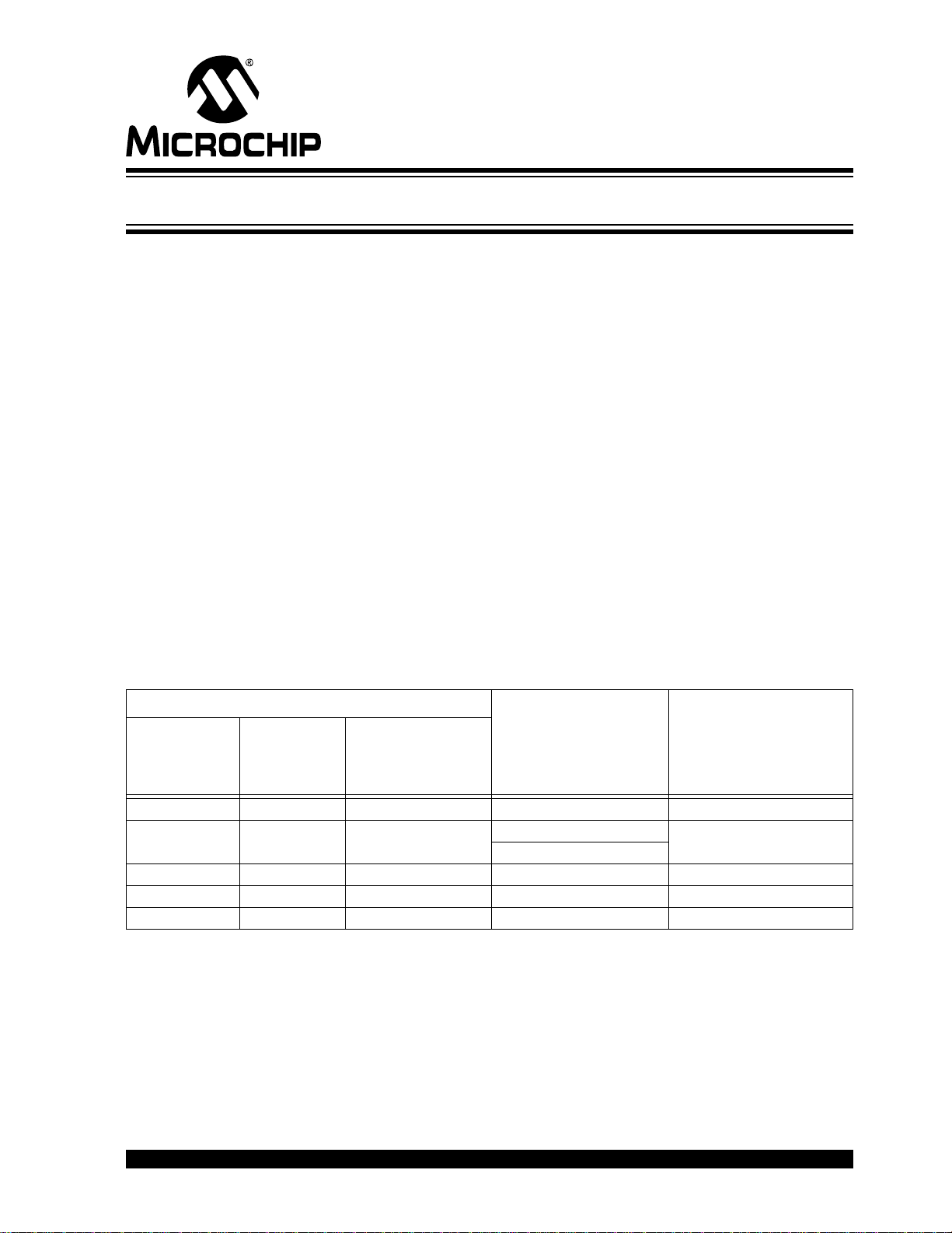
CONVENTIONS USED IN THIS GUIDE
This manual uses the following docum entation conventions:
DOCUMENTATION CONVENTIONS
Description Represents Examples
Arial font:
Italic chara c ters Referenced books MPLAB
Emphasized text ...is the only comp ile r...
Initial caps A window the Output window
A dialog the Settings dialog
A menu selection select Enable Programmer
Quotes A field name in a window or
dialog
Underlined, italic text with
right angle bracket
Bold characters A dialog button Click OK
N‘Rnnnn A number in verilog format,
Text in angle brackets < > A key on the keyboard Press <Enter>, <F1>
Courier New font:
Plain Courier New Sample source code #define START
Italic Courier New A variable argument file.o, where file can be
Square brackets [ ] Optional arguments mcc18 [options] file
Curly brackets and pipe
character: { | }
Ellipses... Replaces r epeated text var_name [,
A menu path File>Save
A tab Click the Power tab
where N is the tota l number of
digits, R is th e radi x and n is a
digit.
Filenames autoexec.bat
File paths c:\mcc18\h
Keywords _asm, _endasm, static
Command-line options -Opa+, -Opa-
Bit values 0, 1
Constants 0xFF, ‘A’
Choice of mutually exclusive
arguments; an OR selection
Represents code supplied by
user
“Save project before build”
4‘b0010, 2‘hF1
any valid filename
[options]
errorlevel {0|1}
var_name...]
void main (void)
{ ...
}
®
IDE User’s Guide
DS50002430A-page 8 2016 Microchip Technology Inc.
Page 9

RECOMMENDED READING
This user’s gui de descri bes how to us e the UC S1003-2 Ev aluation Board. Oth er useful
documents are listed below. The following Microchip documents are available and
recommended as suppl emental r eference resources.
• UCS1003-1/2/3 Data Sheet – “USB Port Power Controller with Charger
Emulation” (DS200005346)
• AN 24.20 – “Using the UCS100x as a Single or Dual Mode Charger”
(DS20005246)
• AN 25.16 – “USB Charging Port ESD Protection Tips for UCS100x”
(DS20005230)
• AN 26.0 – “UCS1002 Current Limit Operation and Features” (DS20005247)
THE MICROCHIP WEB SITE
Microchip provides online support via our web site at www.microchip.com. This web
site is used as a means to make files and information easily available to customers.
Accessible by using your favorite Internet browser, the web site contains the following
information:
• Product Support – Data sheets and errata, application notes and sample
programs, design resources, user’s guides and hardware support documents,
latest software releases and archived software
• General Technical Support – Frequently Asked Questions (FAQs), technical
support requests, online discussion groups, Microchip consultant program
member listing
• Business of Microchip – Product selector and ordering guides, latest Microchip
press releases, list ing of seminars and events, listings of Microchip sales offices,
distributors and factory representatives
Preface
CUSTOMER SUPPORT
Users of Microchip products can receive assistance through several channels:
• Distributor or Representative
• Local Sales Office
• Field Application Engineer (FAE)
• Technical Support
Customers should contact their distributor, representative or field application engineer
(FAE) for support. Local sales offices are also available to help customers. A listing of
sales offices and locations is included in the back of this document.
Technical support is available through the web site at:
http://www.microchip.com/support.
DOCUMENT REVISION HISTORY
Revision A (March 2016)
• Initial Release of this Document.
2016 Microchip Technology Inc. DS50002430A-page 9
Page 10

UCS1003-2 Evaluation Board User’s Guide
NOTES:
DS50002430A-page 10 2016 Microchip Technology Inc.
Page 11

Chapter 1. Product Overview
Tablet or
Smartphone
DC 5V, 3A
Optional
Optional Connectio n to a
5V Power Supply
1.1 INTRODUCTION
The UCS1003-2 device is a Universal Serial Bus (USB) port power switch with charger
emulation. All of the functions of the UCS1003-2 device can be tested and observed
with the UCS1003-2 Evaluation Board. A block diagram of this evaluation board test
setup is shown in Figure 1-1.
UCS1003-2 EVALUATION BOARD
USER’S GUIDE
FIGURE 1-1: UCS1003-2 Evaluation Board – Charger Emulation Test Setup Block Diagram.
1.2 EVALUATION SYSTEM FEATURES
2016 Microchip Technology Inc. DS50002430A-page 11
The evaluation setup is comprised of the UCS1003-2 Evaluation Board and a
downstream tablet or cell phone device, which allows the user to:
• Observe the Charger Emulat io n func tion al ity
• Observe the BC1.2 Charging Downstream Port (CDP), Dedicated Charging Port
(DCP) and Standard Downstream Port (SDP) functionality
• Observe the USB Pass-Through functionality
The hardware platform provides the following features to the user:
• Jumpers for Modes of Operation: Dedicated Charger Emulation (DCE), DCP , CDP
and USB Pass-Through
• Jumper for Fault Handling: Latch upon Fault or Auto-Recovery
• Jumper for Current-Limiting of 0.57A to 2.85A
• Jumper for PWR_EN
Page 12

UCS1003-2 Evaluation Board User’s Guide
1.3 WHAT THE UCS1003-2 EVALUATION BOARD KIT CONTAINS
This UCS1003-2 Evaluation Board Kit includes:
• UCS1003-2 Evaluation Board (ADM00669)
• Provided 5V Wall Power Adapter
• Important Information Sheet
DS50002430A-page 12 2016 Microchip Technology Inc.
Page 13

UCS1003-2 EVALUATION BOARD
USER’S GUIDE
Chapter 2. Installation and Operation
2.1 GETTING STARTED
2.1.1 System Requirements
To use the UCS1003-2 Evaluation Board, the following are required:
• A 5V supply capable of 5V, 3.0A, or the wall transformer provided in the
evaluation kit.
• Various downstream USB devices to charge, such as tablets and cell phones.
• A PC with a USB port to demonstrate CDP, SDP or USB Enumeration.
2.1.2 Evaluation Board Jumper Configuration
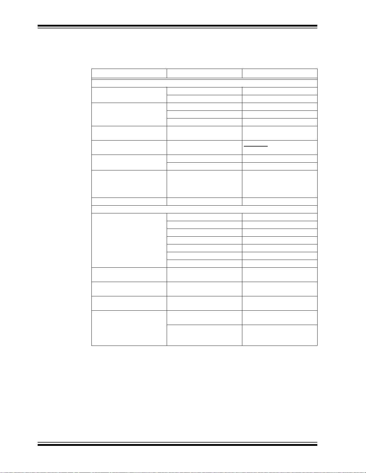
Table 2-1 describes each jumper setting used with this evaluation board.
TABLE 2-1: UCS1003-2 EVALUATION BOARD JUMPER DESCRIPTION
Jumper
Designator
(2)
J5
(1)
J7
(2)
J8
J11 1-2 PWR_EN Enables or disables the port power switch;
(1)
J12
(1)
J13
J14 1-2 LATCH Jumper Placed = Logic Low: LATCH = 0, auto-recovery enabled
Note 1: Each of the J7, J12 and J13 headers must be populated with one jumper for the UCS1003-2 Evaluation
Board to be functional.
2: The headers that select the power supply source (J5 and J8) must always have 2 jumpers populated on
them in total. For more information, see Section 3.1.1 “Power Source”.
Jumper
Position
1-2 V
1-3 VS, V
3-4 V
1-2 V
1-2 V
2-3 V
3-4 EM_EN These pins determine Active mode selection (Dedicated Charger
5-6 M1
7-8 M2
1-2 SEL Jumper Placed = Logic Low: PWR_EN is active-low
2-3 Jumper Placed = Logic High: PWR_EN is active-high
— ILIM Current limit selection between 0.57A to 2.85A (typical)
3-4 S0 Jumper Placed = Logic Low: S0 = 0, Active mode
Pin Name Function Description
S
DD
BUS
S
S
VS connected to 5V bench power supply
VS and VDD tied together
DD
V
connected to 5V bench power supply
DD
V
pins of the UCS1003-2 connected to the V
BUS
USB connector
VS supply connected to the V
VS connected to the 5V input jack
Jumper Placed = Logic Low: PWR_EN polarity is set by the SEL pin
(see jumper J12)
Emulation, Data Pass-Throug h, BC 1.2 SDP, CDP, DCP);
Jumper Placed = Logic Low
Jumper Open = Logic High: LATCH = 1, auto-recovery disabled
Jumper Open = Logic High: S0 = 1, Detect mode
of the USB host
BUS
BUS
of the
2016 Microchip Technology Inc. DS50002430A-page 13
Page 14
DS50002430A-page 14 2016 Microchip Technology Inc.
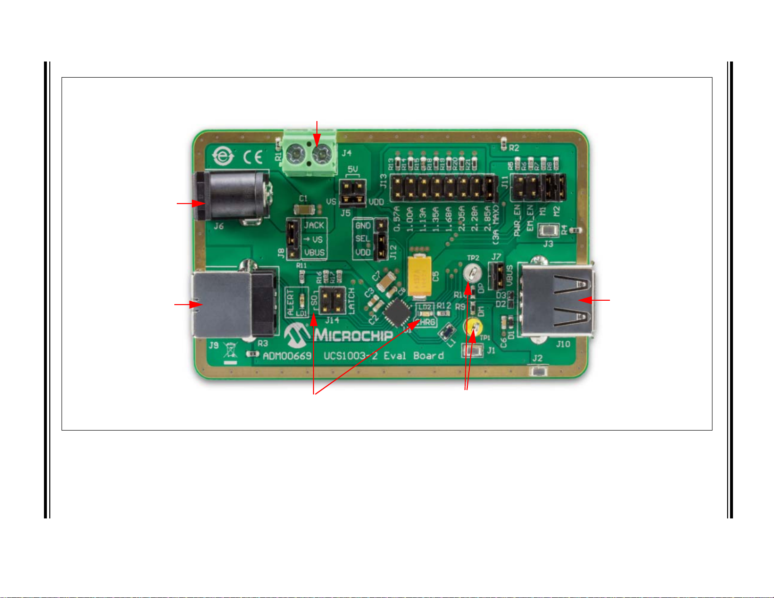
J4
Auxiliary Power Connector to
Bench Power Supply
DP and DM Te st Points
ALERT and CHRG LEDs
J6
Auxiliary Power Connector
to AC-DC
5V Power Supply
J9
USB Standard-B
Receptacle to
USB Host/USB Power
J10
USB Standard-A
Receptacle to Portable
Device
Refer to Figure 2-1 for the jumper location.
UCS1003-2 Evaluation Board User’s Guide
FIGURE 2-1: UCS1003-2 Evaluation Board Test Setup.
Page 15

Installation and Operation
2.1.3 Configuration for Dedicated Charger Emulation (DCE) Mode
The Dedicated Charger Emulation (DCE) mode configures the UCS1003-2
Evaluation Board to cycle through emulation profiles until the charging current
increases above the threshold of 175 mA. T o configure the evaluation board for
the DCE mode, follow these steps:
1. Configure the jumper settings as shown in Table 2-2.
2. Apply 5V. The UCS1003-2 is set to the Detect state and awaits a
downstream device attachment.
3. Connect a tablet or a cell phone to the USB port J10.
When a charger emulation profile is applied and the charging current increases
above 175 mA, LD2 (labeled CHRG) will illuminate and charging will continue.
TABLE 2-2: UCS1003-2 EVALUATION BOARD JUMPER DESCRIPTION FOR DCE MODE
Jumper
Designator
J7 1-2 V
J1 1 1-2 PWR_EN Jumper Open = Logic High: Port power switch enabled
J12 2-3 SEL Jumper Placed = Logic High: PWR_EN is active-high
J13 15-16 ILIM Jumper Placed on Positions 15-16 and not placed on all the other
J14 1-2 LATCH Jumper Placed = Logic Low: LATCH = 0, auto-recovery enabled
Note 1: The power source selection is not mentioned in this table. The headers that select the power supply
source (J5 and J8) must always have 2 jumpers populated on them in total. For more information, see
Section 3.1.1 “Power Source”.
Jumper
Position
3-4 EM_EN Jumper Open = Logic High
5-6 M1 Jumper Placed = Logic Low
7-8 M2 Jumper Placed = Logic Low
3-4 S0 Jumper Open = Logic High: S0 = 1, Detect mode
Pin Name Function Description
BUS
Jumper Placed = V
USB connector
pins of the header J13: Current limit selection is set to 2.85A typical
(3A maximum)
pins of the UC S c onn ec ted to th e V
BUS
(1)
BUS
of the
2016 Microchip Technology Inc. DS50002430A-page 15
Page 16

UCS1003-2 Evaluation Board User’s Guide
2.1.4 Configuration for BC1.2 Charging Downstream Port (CDP) Mode
The Charging Downstream Port (CDP) mode configures the UCS1 003-2
Evaluation Board to handshake respond, enumerate the USB and charge the
downstream device. To configure the evaluation board for the CDP mode,
follow these steps:
1. Configure the jumper settings as shown in Table 2-3.
2. Connect a cable from USB port J9 (USB-B) to an upstream PC USB port.
3. Apply 5V. The UCS1003-2 is set to the Active state and awaits a
downstream device to provide handshake stimulus on the DP pin upon
attachment.
TABLE 2-3: UCS1003-2 EVALUATION BOARD JUMPER DESCRIPTION FOR CDP MODE
Jumper
Designator
J7 1-2 V
J1 1 1-2 PWR_EN Jumper Open = Logic High: Port power switch enabled
J12 2-3 SEL Jumper Placed = Logic High: PWR_EN is active-high
J13 15-16 ILIM Jumper Placed on Positions 15-16 and not placed on all the other
J14 1-2 LATCH Jumper Placed = Logic Low: LATCH = 0, auto-recovery enabled
Note 1: The power source selection is not mentioned in this table. The headers that select the power supply
source (J5 and J8) must always have 2 jumpers populated on them in total. For more information, see
Section 3.1.1 “Power Source”.
Jumper
Position
3-4 EM_EN Jumper Open = Logic High
5-6 M1 Jumper Placed = Logic High
7-8 M2 Jumper Placed = Logic High
3-4 S0 Jumper Open = Logic High: S0 = 0, Active mode
Pin Name Function Description
BUS
Jumper Placed = V
USB connector
pins of the header J13: Current limit selection is set to 2.85A typical
(3A maximum)
pins of the UC S c onn ec ted to th e V
BUS
(1)
BUS
of the
DS50002430A-page 16 2016 Microchip Technology Inc.
Page 17

Installation and Operation
2.1.5 Configuration for BC1.2 Dedicated Charging Port (DCP) Mode
The Dedicated Charging Port (DCP) mode configures the UCS1003-2 Evaluation
Board to handshake respond and charge the downstream device. The DCP is
similar to the Chinese Telecommunications Industry Standard YD/T
1591-2009. To configure the evaluation board for the DCP mode, follow these
steps:
1. Configure the jumper settings as shown in Table 2-4.
2. Apply 5V. The UCS1003-2 is set to the Active state and awaits a
downstream device to handshake upon attachment.
3. Connect a tablet or a cell phone to the USB port J10.
TABLE 2-4: UCS1003-2 EVALUATION BOARD JUMPER DESCRIPTION FOR DCP MODE
Jumper
Designator
J7 1-2 V
J1 1 1-2 PWR_EN Jumper Open = Logic High: Port power switch enabled
J12 2-3 SEL Jumper Placed = Logic High: PWR_EN is active-high
J13 15-16 ILIM Jumper Placed on Positions 15-16 and not placed on all the other
J14 1-2 LATCH Jumper Placed = Logic Low: LATCH = 0, auto-recovery enabled
Note 1: The power source selection is not mentioned in this table. The headers that select the power supply
source (J5 and J8) must always have 2 jumpers populated on them in total. For more information, see
Section 3.1.1 “Power Source”.
Jumper
Position
3-4 EM_EN Jumper Open = Logic High
5-6 M1 Jumper Placed = Logic Low
7-8 M2 Jumper Placed = Logic High
3-4 S0 Jumper Open = Logic High: S0 = 0, Active mode
Pin Name Function Description
BUS
Jumper Placed = V
USB connector
pins of the header J13: Current limit selection is set to 2.85A typical
(3A maximum)
pins of the UC S c onn ec ted to th e V
BUS
(1)
BUS
of the
2016 Microchip Technology Inc. DS50002430A-page 17
Page 18

UCS1003-2 Evaluation Board User’s Guide
2.1.6 Configuration for BC1.2 SDP Mode
The Standard Downstream Port (SDP) mode con figures the UCS1003- 2
Evaluation Board to close the high-speed switch and allow the USB to
enumerate. To configure the evaluation board for the SDP mode, follow these
steps:
1. Configure the jumper settings as shown in Table 2-5.
2. Connect a cable from USB port J9 (USB-B) to an upstream PC USB port.
3. Apply 5V. The UCS1003-2 is set to the Active state and awaits a
downstream device to enumerate the USB upon attachment.
TABLE 2-5: UCS1003-2 EVALUATION BOARD JUMPER DESCRIPTION FOR SDP MODE
Jumper
Designator
J7 1-2 V
J1 1 1-2 PWR_EN Jumper Open = Logic High: Port power switch enabled
J12 2-3 SEL Jumper Placed = Logic High: PWR_EN is active-high
J13 15-16 ILIM Jumper Placed on Positions 15-16 and not placed on all the other
J14 1-2 LATCH Jumper Placed = Logic Low: LATCH = 0, auto-recovery enabled
Note 1: The power source selection is not mentioned in this table. The headers that select the power supply
source (J5 and J8) must always have 2 jumpers populated on them in total. For more information, see
Section 3.1.1 “Power Source”.
Jumper
Position
3-4 EM_EN Jumper Open = Logic Low
5-6 M1 Jumper Placed = Logic High
7-8 M2 Jumper Placed = Logic Low
3-4 S0 Jumper Open = Logic Low: S0 = 0, Active mode
Pin Name Function Description
BUS
Jumper Placed = V
USB connector
pins of the header J13: Current limit selection is set to 2.85A typical
(3A maximum)
pins of the UC S c onn ec ted to th e V
BUS
(1)
BUS
of the
DS50002430A-page 18 2016 Microchip Technology Inc.
Page 19
Chapter 3. Hardware Overview
3.1 INTRODUCTION
The UCS1003-2 Evaluation Board provides the means to demonstrate all of the
UCS1003-2 functionality. The LEDs indicate the status information.
3.1.1 Power Source
The UCS1003-2 Evaluation Board requires 5V, 3.0A. It has two power supply
connectors:
• J6 jack for AC-DC wall adapters
• J4 for connection with wires from a laboratory power supply
The board allows using only one of these power supplies or both (for the evaluating split
supply feature).
According to the note from the Electrical Characteristics table from the data sheet, for
split supply systems using the Attach Detection feature, the V
V
+ 150 mV. If this condition cannot be met, then VDD and VS can be tied together,
DD
to avoid a voltage difference higher than 150 mV between them.
The V
S
headers. The two headers must always have two jumpers populated on them in total.
The board is not functional if the jumpers are populated in other configurations. See
Table 3-1 for J5 and J8 jumper options.
UCS1003-2 EVALUATION BOARD
USER’S GUIDE
must not exceed
S
and VDD supply source is selected by populating jumpers on the J5 and J8
TABLE 3-1: POWER SUPPLY SELECTION OPTIONS WITH J5 AND J8 HEADERS
Available Power Source(s)
AC-DC Adapter
Connected to
Jack J6
Yes No No 1-3 (V
No No Yes 1-2 (VS tied to 5V)
Yes No Yes 3-4 (VDD tied to 5V)
No Yes Yes 3-4 (VDD tied to 5V)
No Yes No 1-3 (VS tied to VDD)
Note 1: Simple setup that can be made with the AC-DC adapter from the UCS1003-2 Evaluation Board Kit.
2: This setup can be used to evaluate the charging process at different supply voltages (up to 5.5 V) and to
have an indication of the charging current from the bench power supply.
3: This setup can be used to evaluate the split power supply feature.
4: This setup can be used only if the USB port connected to jumper J9 is capable of delivering the required
charging current.
USB Port
Connected to
Jumper J9
Bench Power
Supply Connected
with Wires to
Connector J4
Populated Positions for
Jumper J5
(1)
(2)
(2)
(3)
(3,4)
(3,4)
3-4 (V
tied to VDD)
S
tied to 5V)
DD
Populated Positions for
Jumper J8
2-3 (VS tied to jack J6)
N/A
2-3 (VS tied to jack J6)
1-2 (VS tied to V
1-2 (VS tied to V
BUS
BUS
(3,4)
)
(3,4)
)
(1)
(3)
2016 Microchip Technology Inc. DS50002430A-page 19
Page 20

UCS1003-2 Evaluation Board User’s Guide
3.2 STAND-ALONE FUNCTIONALITY
The UCS1003-2 is intended for the stand-alone USB charger and BC1.2 CDP, DCP
and SDP applications. The green LED (LD2 – CHRG) indicates that the charging
current has exceeded the 175 mA threshold (I
See Table 2-1 for the description of jumpers.
3.2.1 Charger Emulation Mode Configurations
The Charger Emulation mode of the UCS1003-2 is controlled by the pin states: M1, M2
and EM_EN. These are the jumpers located on the J11 header.
3.2.2 Attach Detection and Power States
The UCS1003-2 can use the attach detection functionality or force the Active mode
power state. This is controlled by jumper J14, position 3-4.
3.3 FAULT HANDLING
The UCS1003-2 has two modes of Fault handling that can be configured for the LATCH
upon Fault or auto-recovery. Jumper J14, position 1-2, selects the Fault handling.
When a Fault condition is detected, the red LED (marked as LD1 – ALERT) turns on.
See Table 2-1 for the description of jumpers.
BUS_CHG
).
3.4 CURRENT LIMITING
The UCS1003-2 is capable of eight selectable current limits (see the “UCS1003-1/2/3
Data Sheet” for detailed information). Jumper J13 selects the current-limiting value.
See Table 2-1 for the description of jumpers.
3.5 HIGH-SPEED USB DATA SWITCH
The UCS1003-2 contains a series of USB 2.0-compliant high-speed switch between
the DP and DM input and output pins. This switch is functional in CDP, SDP and USB
pass-through configurations. When used in one of these configurations, a port from a
PC must be connected to the J9 USB connector.
DS50002430A-page 20 2016 Microchip Technology Inc.
Page 21

Appendix A. Schematics and Layouts
A.1 INTRODUCTION
This appendix contains the following schematics and layouts for the UCS1003-2
Evaluation Board:
• Board – Schematic
• Board – Top Silk
• Board – Top Silk and Copper
• Board – Top Copper
• Board – Bottom Copper
• Board – Bottom Silk and Copper
• Board – Bottom Silk
UCS1003-2 EVALUATION BOARD
USER’S GUIDE
2016 Microchip Technology Inc. DS50002430A-page 21
Page 22

DS50002430A-page 22 2016 Microchip Technology Inc.
M1
1
M2
2
V
BUS
1
3
V
BUS
2
4
VS1
7
VS2
8
V
DD
9
GND
20
DPIN
14
DMIN
15
DMOUT
16
DPOUT
17
EM_EN
19
ILIM
5
SEL
6
PWR_EN
10
ALERT
13
LATCH
11
CHRG
18
S0
12
EP
21
UCS1003-2
U1
123
HDR-2.54 Male 1x3
J8
12
34
HDR-2.54 Male 2x2
J5
1 2
3 4
5 6
7 8
HDR-2.54 Male 2x4
J11
V
BUS
1
GND
4
D-
2
D+
3
0
USB2.0-A
J10
V
BUS
1
GND
4
D-
2
D+
3
0
USB2.0-B
J9
2
3
1
POWER 2.1 mm
J6
21
TERMINAL 5 mm Female 1x2
J4
GND
GND
0.01 μF
16V
0603
C8
GND GND
1 μF
25V
0603
C3
0.1 μF
16V
0603
C2
GND GND
GND
150 μF
10V
TANT-D
C5
GND
470 pF
50V
0603
C6
GND
L2L2'
L1L1'
CM Choke 90Ohm
L1
GND SHIELD
0R
0603
R4
GNDSHIELD
0R
0603
R3
GNDSHIELD
0R
0603
R1
GNDSHIELD
0R
0603
R2
1
J2
1
J1
1
J3
GND
GND
TP LOOP White
TP2
DP
TP LOOP Yellow
TP1
DM
1M
0603
5%
R9
1M
0603
5%
R10
1k
0603
5%
R11
VDD_5V
VDD_5V
1k
0603
5%
R12
VDD_5V
RED
LD1
GREEN
LD2
10k
0603
5%
R5
VDD_5V
GND
10k
0603
5%
R6
10k
0603
5%
R7
10k
0603
5%
R8
Rubber Pad Cyl D7.9H5.3
PAD2
Rubber Pad Cyl D7.9H5.3
PAD4
Rubber Pad Cyl D7.9H5.3
PAD1
Rubber Pad Cyl D7.9H5.3
PAD3
Shunt 2.54 mm 1x2 Handle10
JP1
5V ONLY
1
2
HDR-2.54 Male 1x2
J7
CHRG#
ALERT#
12
34
HDR-2.54 Male 2x2
J14
10k
0603
5%
R16
10k
0603
5%
R17
VDD_5V
GND
123
HDR-2.54 Male 1x3
J12
VDD_5V
GND
1
2
3
4
5
6
7
8
9
10
11
12
13
14
15
16
HDR-2.54 Male 2x8
J13
VDD_5V
47k
R13
56k
R14
68k
R15
82k
R18
100k
R19
120k
R20
150k
R21
GND
0.57A
1.00A
1.13A
1.35A
1.68A
2.05
2.28
2.85A (3A MAX)
10 μF
10V
1206
C7
5V
SOD-523
D1
5V
SOD-882
D2
5V
SOD-882
D3
SHIELD
SHIELDSHIELD
VS
D_OUT_N
D_OUT_PD_IN_P
D_IN_N D_OUT_N
D_OUT_P
5V_JACK
5V_TERMINAL
47 μF
10V
1206
C1
PWR_EN
EM_EN
M1
M2
V
BUS
SO
LATCH
ILIM
SEL
5V-3A
PS1
INTERCHANGEABLE BLADES KIT
ADAPTER1
UCS1003-2 Evaluation Board User’s Guide
A.2 BOARD – SCHEMATIC
Page 23

A.3 BOARD – TOP SILK
Schematics and Layouts
A.4 BOARD – TOP SILK AND COPPER
2016 Microchip Technology Inc. DS50002430A-page 23
Page 24

UCS1003-2 Evaluation Board User’s Guide
A.5 BOARD – TOP COPPER
A.6 BOARD – BOTTOM COPPER
DS50002430A-page 24 2016 Microchip Technology Inc.
Page 25

A.7 BOARD – BOTTOM SILK AND COPPER
Schematics and Layouts
A.8 BOARD – BOTTOM SILK
2016 Microchip Technology Inc. DS50002430A-page 25
Page 26

UCS1003-2 Evaluation Board User’s Guide
NOTES:
DS50002430A-page 26 2016 Microchip Technology Inc.
Page 27

UCS1003-2 EVALUATION BOARD
USER’S GUIDE
Appendix B. Bill of Materials (BOM)
TABLE B-1: BILL OF MATERIALS (BOM)
Qty. Designator Description Manufacturer Part Number
1 C1 Cap. Ceramic, 47 µF , 10V, 20%, X5R SMD, 1206 KEMET
1 C2 Cap. Ceramic, 0.1µF, 16V, 10%, X7R SMD, 0603 AVX Corporation 0603YC104KAT2A
1 C3 Cap. Ceramic, 1µF, 25V, 10%, X7R SMD, 0603 TDK Corporation C1608X7R1E105K
1 C5 Cap. Tantalum, 150 µF, 10V, 10%, 100m, SMD D AVX Corporation TPSD157K010R0100
1 C6 Cap. Ceramic, 470pF, 50V, 10%, X7R SMD, 0603 Johanson
Dielectrics
1 C7 Cap. Ceramic, 10 µF, 10V, 20%, X7R SMD, 1206 Murata GRM31CR71A106KA01L
1 C8 Cap. Ceramic, 0.0 1µF, 16V, 10%, X7R SMD, 0603 Samsung
Electro-Mechanics
America, Inc.
1 D1 Diode Zener , T5V0 S5-7, 5V, 150 mW, SMD,
SOD-523
2 D2, D3 Diode Zener, PESD5V0X1BL, 5V, SMD, SOD-882 NXP Semiconductors PESD5V0X1BL,315
3 J1, J2, J3 Conn. TP Loop, Tin, SMD Harwin Plc. S1751-46R
1 J4 Conn. Terminal, 5 mm, 18A, Female,
1x2 TH, R/A
2 J5, J14 Conn. Header-2.54, Male, 2x2, Gol d, 5.8 4MH TH,
Vertical
1 J6 Conn. Power, 2.1 mm, 5.5 mm, Switch, TH, R/A CUI Inc. PJ-002A
1 J7 Conn. Header-2.54, Male, 1x2, Tin, 6.10 MH TH,
Vertical
2 J8, J12 Conn. Header-2.54, Male, 1x3, Tin, 5.84 MH TH,
Vertical
1 J9 Conn. USB 2.0, STD-A, Female, TH, R/A TE Connectivity, Ltd. 292304-1
1 J10 Conn. USB 2.0, STD-A, Female, TH, R/A FCI 87520-0010BLF
1 J11 Conn. Header-2.54, M ale , 2 x4 , G ol d, 5.8 4 MH TH,
Vertical
1 J13 Conn. Header-2.54, Male, 2 x8 , G ol d, 5.8 4 MH TH,
Vertical
1 L1 Inductor Choke, Common Mode, 90k, 0805 Murata Electronics
1 LD1 Diode LED, Red, 1.95V, 30 mA, 700 mcd, Clear,
SMD, 0603
1 LD2 Diode LED, Green, 2.2V, 25 mA, 15 mcd, Clear,
SMD, 0603
1 PCB UCS1001-3 – Printed Circuit Board — 04-10421
4R1, R2,
R3, R4
Note: The components listed in this Bill of Materials are representative of the PCB assembly. The released BOM
Resistor TKF, 0R, 1/10W, SMD, 0603 NIC Components
used in manufacturing uses all RoHS-compliant components.
Diodes
Phoenix Contact 1935161
Samtec, Inc. HTSW-102-07-G-D
Molex
Samtec, inc. TSW-103-07-T-S
Samtec, inc. TSW-104-08-L-D
FCI 68602-116HLF
Kingbright Corp. APTD1608SURCK
Kingbright Corp. APT1608SGC
Corp.
®
®
Incorporated T5V0S5-7
®
C1206C476M8PACTU
500R14W471KV4T
CL10B103KO8NNNC
0022284020
®
DL W21HN900SQ2L
NRC06Z0TRF
2016 Microchip Technology Inc. DS50002430A-page 27
Page 28

UCS1003-2 Evaluation Board User’s Guide
TABLE B-1: BILL OF MATERIALS (BOM) (CONTINUED)
Qty. Designator Description Manufacturer Part Number
6 R5, R6, R7,
R8, R16,
R17
2 R9, R10 Resistor TKF, 1M, 5%, 1/10W, SMD, 0603 Yageo Corporation 9C06031A1004JLHFT
2 R11, R12 Resistor TKF, 1k, 5%, 1/10W, SMD, 0603 Panasonic - ECG ERJ-3GEYJ102V
1 R13 Resistor TKF, 47k, 1%, 1/10 W, SMD, 0603 Panasonic - ECG ERJ-3EKF4702V
1 R14 Resistor TKF, 56k, 1%, 1/10 W, SMD, 0603 Sta ck po le
1 R15 Resistor TKF, 68k, 1%, 1/10 W, SMD, 0603 Sta ck po le
1 R18 Resistor TKF , 82k,1%, 1/10W, SMD, 0603 Panasonic Electronic
1 R19 Resistor TKF, 100k, 1%, 1/10W, SMD, 0603 Panasonic - ECG ERJ-3EKF1003V
1 R20 Resistor TKF, 120k, 1%, 1/10W, SMD, 0603 Panasonic - ECG ERJ-3EKF1203V
1 R21 Resistor TKF, 150k,1%, 1/10W, SMD, 0603 Panasonic - ECG ERJ-3EKF1503V
1 TP1 Conn. TP Loop, Yellow, TH Keystone
1 TP2 Conn. TP Loop, White, TH Keystone 5012
1 U1 Microchip Interface USB Power Switch,
Note: The components listed in this Bill of Materials are representative of the PCB assembly. The released BOM
Resistor TKF, 10k, 5%, 1/10W, SMD, 0603 Panasonic
Electronics, Inc.
Electronics, Inc.
Components
Electronics Corp.
Microchip
UCS1003-2-BP QFN-20
used in manufacturing uses all RoHS-compliant components.
Technology Inc.
®
- ECG ERJ-3GEYJ103V
RMCF0603FT56K0
RMCF0603FT68K0
ERJ-3EKF8202V
5014
UCS1003-2-BP
TABLE B-2: BILL OF MATERIALS – MECHANICAL PARTS
Qty. Designator Description Manufacturer Part Number
1 ADAPTER1 Mechanical HW Adapter Inte rchangeable B lades Kit for
Phihong R-series Wall Adapters
10 JP1 Mechanical HW Jumper, 2.54 mm, 1x2, Handle Gold TE Connectivity 881545-2
4 PAD1, PAD2,
PAD3, PAD4
1 PS1 Mechanical HW Power Supply, 5V, 3A, DC, 2.1 mm Phihong USA Inc. PSA15R-050PV
Note 1: The components listed in this Bill of Materials are representative o f th e PCB assembly. The released BOM
used in manufacturing uses all RoHS-compliant components.
Mechanical HW Rubber Pad, Cylind ric al, D7.9 H 5.3,
Black
Phihong USA Inc. RPBAG
3M SJ61A11
DS50002430A-page 28 2016 Microchip Technology Inc.
Page 29

NOTES:
Bill of Materials (BOM)
2016 Microchip Technology Inc. DS50002430A-page 29
Page 30

Worldwide Sales and Service
AMERICAS
Corporate Office
2355 West Chandler Blvd.
Chandler, AZ 85224-6199
Tel: 480-792-7200
Fax: 480-792-7277
Technical Support:
http://www.microchip.com/
support
Web Address:
www.microchip.com
Atlanta
Duluth, GA
Tel: 678-957-9614
Fax: 678-957-1455
Austin, TX
Tel: 512-257-3370
Boston
Westborough, MA
Tel: 774-760-0087
Fax: 774-760-0088
Chicago
Itasca, IL
Tel: 630-285-0071
Fax: 630-285-0075
Cleveland
Independence, OH
Tel: 216-447-0464
Fax: 216-447-0643
Dallas
Addison, TX
Tel: 972-818-7423
Fax: 972-818-2924
Detroit
Novi, MI
Tel: 248-848-4000
Houston, TX
Tel: 281-894-5983
Indianapolis
Noblesville, IN
Tel: 317-773-8323
Fax: 317-773-5453
Los Angeles
Mission Viejo, CA
Tel: 949-462-9523
Fax: 949-462-9608
New York, NY
Tel: 631-435-6000
San Jose, CA
Tel: 408-735-9110
Canada - Toronto
Tel: 905-673-0699
Fax: 905-673-6509
ASIA/PACIFIC
Asia Pacific Office
Suites 3707-14, 37th Floor
Tower 6, The Gateway
Harbour City, Kowloon
Hong Kong
Tel: 852-2943-5100
Fax: 852-2401-3431
Australia - Sydney
Tel: 61-2-9868-6733
Fax: 61-2-9868-6755
China - Beijing
Tel: 86-10-8569-7000
Fax: 86-10-8528-2104
China - Chengdu
Tel: 86-28-8665-5511
Fax: 86-28-8665-7889
China - Chongqing
Tel: 86-23-8980-9588
Fax: 86-23-8980-9500
China - Dongguan
Tel: 86-769-8702-9880
China - Hangzhou
Tel: 86-571-8792-8115
Fax: 86-571-8792-8116
China - Hong Kong SAR
Tel: 852-2943-5100
Fax: 852-2401-3431
China - Nanjing
Tel: 86-25-8473-2460
Fax: 86-25-8473-2470
China - Qingdao
Tel: 86-532-8502-7355
Fax: 86-532-8502-7205
China - Shanghai
Tel: 86-21-5407-5533
Fax: 86-21-5407-5066
China - Shenyang
Tel: 86-24-2334-2829
Fax: 86-24-2334-2393
China - Shenzhen
Tel: 86-755-8864-2200
Fax: 86-755-8203-1760
China - Wuhan
Tel: 86-27-5980-5300
Fax: 86-27-5980-5118
China - Xian
Tel: 86-29-8833-7252
Fax: 86-29-8833-7256
ASIA/PACIFIC
China - Xiamen
Tel: 86-592-2388138
Fax: 86-592-2388130
China - Zhuhai
Tel: 86-756-3210040
Fax: 86-756-3210049
India - Bangalore
Tel: 91-80-3090-4444
Fax: 91-80-3090-4123
India - New Delhi
Tel: 91-11-4160-8631
Fax: 91-11-4160-8632
India - Pune
Tel: 91-20-3019-1500
Japan - Osaka
Tel: 81-6-6152-7160
Fax: 81-6-6152-9310
Japan - Tokyo
Tel: 81-3-6880- 3770
Fax: 81-3-6880-3771
Korea - Daegu
Tel: 82-53-744-4301
Fax: 82-53-744-4302
Korea - Seoul
Tel: 82-2-554-7200
Fax: 82-2-558-5932 or
82-2-558-5934
Malaysia - Kuala Lumpur
Tel: 60-3-6201-9857
Fax: 60-3-6201-9859
Malaysia - Penang
Tel: 60-4-227-8870
Fax: 60-4-227-4068
Philippines - Manila
Tel: 63-2-634-9065
Fax: 63-2-634-9069
Singapore
Tel: 65-6334-8870
Fax: 65-6334-8850
Taiwan - Hsin Chu
Tel: 886-3-5778-366
Fax: 886-3-5770-955
Taiwan - Kaohsiung
Tel: 886-7-213-7828
Taiwan - Taipei
Tel: 886-2-2508-8600
Fax: 886-2-2508-0102
Thailand - Bangkok
Tel: 66-2-694-1351
Fax: 66-2-694-1350
EUROPE
Austria - Wels
Tel: 43-7242-2244-39
Fax: 43-7242-2244-393
Denmark - Copenhagen
Tel: 45-4450-2828
Fax: 45-4485-2829
France - Paris
Tel: 33-1-69-53-63-20
Fax: 33-1-69-30-90-79
Germany - Dusseldorf
Tel: 49-2129-3766400
Germany - Karlsruhe
Tel: 49-721-625370
Germany - Munich
Tel: 49-89-627-144-0
Fax: 49-89-627-144-44
Italy - Milan
Tel: 39-0331-742611
Fax: 39-0331-466781
Italy - Venice
Tel: 39-049-7625286
Netherlands - Drunen
Tel: 31-416-690399
Fax: 31-416-690340
Poland - Warsaw
Tel: 48-22-3325737
Spain - Madrid
Tel: 34-91-708-08-90
Fax: 34-91-708-08-91
Sweden - Stockholm
Tel: 46-8-5090-4654
UK - Wokingham
Tel: 44-118-921-5800
Fax: 44-118-921-5820
07/14/15
DS50002430A-page 30 2016 Microchip Technology Inc.
 Loading...