

Microchip Technology TO220-3 Voltage Regulator Evaluation Board, TO263-3 Voltage Regulator Evaluation Board User guide
Page 1

TO220-3/TO263-3
Voltage Regulator
Evaluation Board
User’s Guide
© 2009 Microchip Technology Inc. DS51818A
Page 2
Note the following details of the code protection feature on Microchip devices:
• Microchip products meet the specification contained in their particular Microchip Data Sheet.
• Microchip believes that its family of products is one of the most secure families of its kind on the market today, when used in the
intended manner and under normal conditions.
• There are dishonest and possibly illegal methods used to breach the code protection feature. All of these methods, to our
knowledge, require using the Microchip products in a manner outside the operating specifications contained in Microchip’s Data
Sheets. Most likely, the person doing so is engaged in theft of intellectual property.
• Microchip is willing to work with the customer who is concerned about the integrity of their code.
• Neither Microchip nor any other semiconductor manufacturer can guarantee the security of their code. Code protection does not
mean that we are guaranteeing the product as “unbreakable.”
Code protection is constantly evolving. We at Microchip are committed to continuously improving the code protection features of our
products. Attempts to break Microchip’s code protection feature may be a violation of the Digital Millennium Copyright Act. If such acts
allow unauthorized access to your software or other copyrighted work, you may have a right to sue for relief under that Act.
Information contained in this publication regarding device
applications and the like is provided only for your convenience
and may be superseded by updates. It is your responsibility to
ensure that your application meets with your specifications.
MICROCHIP MAKES NO REPRESENTATIONS OR
WARRANTIES OF ANY KIND WHETHER EXPRESS OR
IMPLIED, WRITTEN OR ORAL, STATUTORY OR
OTHERWISE, RELATED TO THE INFORMATION,
INCLUDING BUT NOT LIMITED TO ITS CONDITION,
QUALITY, PERFORMANCE, MERCHANTABILITY OR
FITNESS FOR PURPOSE. Microchip disclaims all liability
arising from this information and its use. Use of Microchip
devices in life support and/or safety applications is entirely at
the buyer’s risk, and the buyer agrees to defend, indemnify and
hold harmless Microchip from any and all damages, claims,
suits, or expenses resulting from such use. No licenses are
conveyed, implicitly or otherwise, under any Microchip
intellectual property rights.
Trademarks
The Microchip name and logo, the Microchip logo, Accuron,
dsPIC, K
EELOQ, KEELOQ logo, MPLAB, PIC, PICmicro,
PICSTART, rfPIC, SmartShunt and UNI/O are registered
trademarks of Microchip Technology Incorporated in the
U.S.A. and other countries.
FilterLab, Hampshire, Linear Active Thermistor, MXDEV,
MXLAB, SEEVAL, SmartSensor and The Embedded Control
Solutions Company are registered trademarks of Microchip
Technology Incorporated in the U.S.A.
Analog-for-the-Digital Age, Application Maestro, CodeGuard,
dsPICDEM, dsPICDEM.net, dsPICworks, dsSPEAK, ECAN,
ECONOMONITOR, FanSense, In-Circuit Serial
Programming, ICSP, ICEPIC, Mindi, MiWi, MPASM, MPLAB
Certified logo, MPLIB, MPLINK, mTouch, nanoWatt XLP,
PICkit, PICDEM, PICDEM.net, PICtail, PIC
32
logo, PowerCal,
PowerInfo, PowerMate, PowerTool, REAL ICE, rfLAB, Select
Mode, Total Endurance, TSHARC, WiperLock and ZENA are
trademarks of Microchip Technology Incorporated in the
U.S.A. and other countries.
SQTP is a service mark of Microchip Technology Incorporated
in the U.S.A.
All other trademarks mentioned herein are property of their
respective companies.
© 2009, Microchip Technology Incorporated, Printed in the
U.S.A., All Rights Reserved.
Printed on recycled paper.
Microchip received ISO/TS-16949:2002 certification for its worldwide
headquarters, design and wafer fabrication facilities in Chandler and
Tempe, Arizona; Gresham, Oregon and design centers in California
and India. The Company’s quality system processes and procedures
are for its PIC
devices, Serial EEPROMs, microperipherals, nonvolatile memory and
analog products. In addition, Microchip’s quality system for the design
and manufacture of development systems is ISO 9001:2000 certified.
®
MCUs and dsPIC® DSCs, KEELOQ
®
code hopping
DS51818A-page ii © 2009 Microchip Technology Inc.
Page 3

TO220-3/TO263-3 VOLTAGE REGULATOR
EVALUATION BOARD USER’S GUIDE
Table of Contents
Preface ........................................................................................................................... 1
Introduction............................................................................................................ 1
Document Layout .................................................................................................. 1
Conventions Used in this Guide ............................................................................ 2
Recommended Reading........................................................................................ 3
The Microchip Web Site ........................................................................................ 3
Customer Support ................................................................................................. 3
Document Revision History................................................................................... 3
Chapter 1. Product Overview
1.1 Introduction ..................................................................................................... 5
1.2 What is the TO220-3/TO263-3 Voltage Regulator Evaluation Board? ........... 5
1.3 What the TO220-3/TO263-3 Voltage Regulator Evaluation Board
kit includes ................................................................................................ 6
Chapter 2. Installation and Operation
2.1 Introduction ..................................................................................................... 7
2.2 Features ......................................................................................................... 7
2.3 Getting Started ............................................................................................... 7
Appendix A. Schematic and Layouts
A.1 Introduction .................................................................................................... 9
A.2 Board - Schematic ....................................................................................... 10
A.3 Board - Top Silk ........................................................................................... 11
A.4 Board - Top Copper ..................................................................................... 12
A.5 Board - Bottom Copper ................................................................................ 13
Appendix B. Bill of Materials (BOM)
Worldwide Sales and Service .................................................................................... 16
© 2009 Microchip Technology Inc. DS51818A-page iii
Page 4

TO220-3/TO263-3 Voltage Regulator Evaluation Board User’s Guide
NOTES:
DS51818A-page iv © 2009 Microchip Technology Inc.
Page 5
TO220-3/TO263-3 VOLTAGE REGULATOR
EVALUATION BOARD USER’S GUIDE
Preface
NOTICE TO CUSTOMERS
All documentation becomes dated, and this manual is no exception. Microchip tools and
documentation are constantly evolving to meet customer needs, so some actual dialogs
and/or tool descriptions may differ from those in this document. Please refer to our web site
(www.microchip.com) to obtain the latest documentation available.
Documents are identified with a “DS” number. This number is located on the bottom of each
page, in front of the page number. The numbering convention for the DS number is
“DSXXXXXA”, where “XXXXX” is the document number and “A” is the revision level of the
document.
For the most up-to-date information on development tools, see the MPLAB
Select the Help menu, and then Topics to open a list of available on-line help files.
®
IDE on-line help.
INTRODUCTION
This chapter contains general information that will be useful to know before using the
TO220-3/TO263-3 Voltage Regulator Evaluation Board. Items discussed in this
chapter include:
• Document Layout
• Conventions Used in this Guide
• Recommended Reading
• The Microchip Web Site
• Customer Support
• Document Revision History
DOCUMENT LAYOUT
This document describes how to use the TO220-3/TO263-3 Voltage Regulator
Evaluation Board as a development tool to emulate and debug firmware on a target
board. The manual layout is as follows:
• Chapter 1. “Product Overview” – Contains information about the
TO220-3/TO263-3 Voltage Regulator Evaluation Board.
• Chapter 2. “Installation and Operation” – Includes instructions on how to get
started with this evaluation board and a description of the evaluation board
operation.
• Appendix A. “Schematic and Layouts” – Shows the schematic and layout
diagrams for the TO220-3/TO263-3 Voltage Regulator Evaluation Board.
• Appendix B. “Bill of Materials (BOM)” – Lists the parts used to build the
TO220-3/TO263-3 Voltage Regulator Evaluation Board.
© 2009 Microchip Technology Inc. DS51818A-page 1
Page 6
TO220-3/TO263-3 Voltage Regulator Evaluation Board User’s Guide
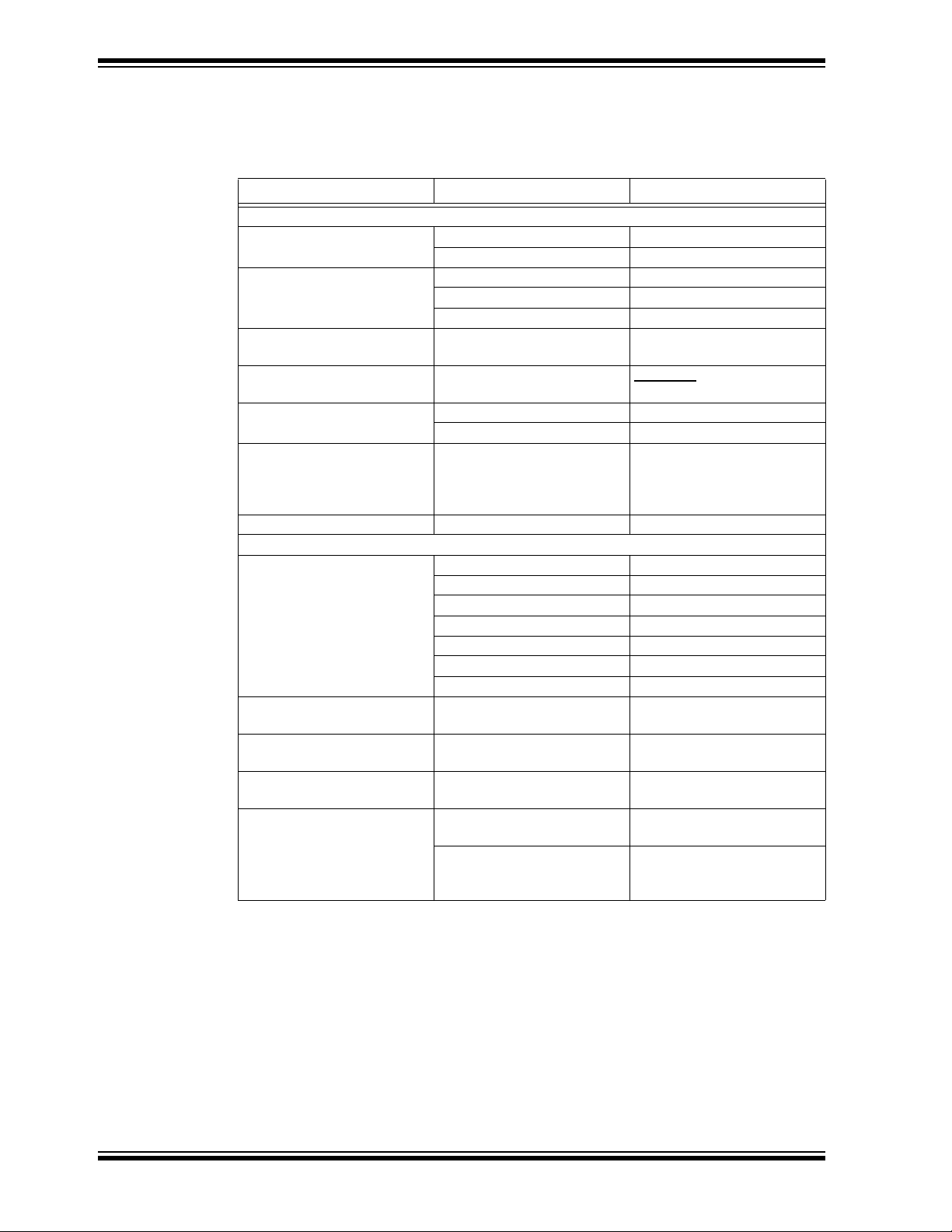
CONVENTIONS USED IN THIS GUIDE
This manual uses the following documentation conventions:
DOCUMENTATION CONVENTIONS
Description Represents Examples
Arial font:
Italic characters Referenced books MPLAB® IDE User’s Guide
Emphasized text ...is the only compiler...
Initial caps A window the Output window
A dialog the Settings dialog
A menu selection select Enable Programmer
Quotes A field name in a window or
dialog
Underlined, italic text with
right angle bracket
Bold characters A dialog button Click OK
N‘Rnnnn A number in verilog format,
Text in angle brackets < > A key on the keyboard Press <Enter>, <F1>
Courier New font:
Plain Courier New Sample source code #define START
Italic Courier New A variable argument file.o, where file can be
Square brackets [ ] Optional arguments mcc18 [options] file
Curly brackets and pipe
character: { | }
Ellipses... Replaces repeated text var_name [,
A menu path File>Save
A tab Click the Power tab
where N is the total number of
digits, R is the radix and n is a
digit.
Filenames autoexec.bat
File paths c:\mcc18\h
Keywords _asm, _endasm, static
Command-line options -Opa+, -Opa-
Bit values 0, 1
Constants 0xFF, ‘A’
Choice of mutually exclusive
arguments; an OR selection
Represents code supplied by
user
“Save project before build”
4‘b0010, 2‘hF1
any valid filename
[options]
errorlevel {0|1}
var_name...]
void main (void)
{ ...
}
DS51818A-page 2 © 2009 Microchip Technology Inc.
Page 7

RECOMMENDED READING
This user's guide describes how to use TO220-3/TO263-3 Voltage Regulator
Evaluation Board. Other useful documents are listed below. The following Microchip
documents are available and recommended as supplemental reference resources.
• MCP1790 Data Sheet - “70 mA, High Voltage Regulator”, DS22075
• MCP1825 Data Sheet - “500 mA, Low Voltage, Low Quiescent Current LDO
Regulator”, DS22056
• MCP1826 Data Sheet - “1000 mA, Low Voltage, Low Quiescent Current LDO
Regulator”, DS22057
• MCP1827 Data Sheet - “1.5A, Low Voltage, Low Quiescent Current LDO
Regulator”, DS22001
These datasheets provide useful information regarding voltage regulator parameters
that may be validated using this evaluation board.
THE MICROCHIP WEB SITE
Microchip provides online support via our web site at www.microchip.com. This web
site is used as a means to make files and information easily available to customers.
Accessible by using your favorite Internet browser, the web site contains the following
information:
• Product Support – Data sheets and errata, application notes and sample
programs, design resources, user’s guides and hardware support documents,
latest software releases and archived software
• General Technical Support – Frequently Asked Questions (FAQs), technical
support requests, online discussion groups, Microchip consultant program
member listing
• Business of Microchip – Product selector and ordering guides, latest Microchip
press releases, listing of seminars and events, listings of Microchip sales offices,
distributors and factory representatives
Preface
CUSTOMER SUPPORT
Users of Microchip products can receive assistance through several channels:
• Distributor or Representative
• Local Sales Office
• Field Application Engineer (FAE)
• Technical Support
Customers should contact their distributor, representative or field application engineer
(FAE) for support. Local sales offices are also available to help customers. A listing of
sales offices and locations is included in the back of this document.
Technical support is available through the web site at: http://support.microchip.com
DOCUMENT REVISION HISTORY
Revision A (April 2009)
• Initial Release of this Document.
© 2009 Microchip Technology Inc. DS51818A-page 3
Page 8

TO220-3/TO263-3 Voltage Regulator Evaluation Board User’s Guide
NOTES:
DS51818A-page 4 © 2009 Microchip Technology Inc.
Page 9

Chapter 1. Product Overview
1.1 INTRODUCTION
The TO220-3 / TO263-3 Voltage Regulator Evaluation Board is designed to provide
functional evaluation of Microchip Voltage Regulators that utilize the TO220-3 and
TO263-3 package and the following device pinouts:
Pin Number U1 footprint
The TO220-3 / TO263-3 Voltage Regulator Evaluation Board does not come with a
voltage regulator soldered onto the board. This allows the user to attach the voltage
regulator of their choosing to the board and perform quiescent current, ground current,
PSRR, and other desired tests.
The TO220-3 / TO263-3 Voltage Regulator Evaluation Board is based upon a modular
concept which will allow the user to plug in additional boards to increase the test
capability of the voltage regulator. Planned additional modulare plugin boards currently
consist of an Input Voltage Linestep Board, Output Voltage Loadstep Board, and
several other device packages.
TO220-3/TO263-3 VOLTAGE REGULATOR
EVALUATION BOARD USER’S GUIDE
Pin 1 V
Pin 2 GND
Pin 3 V
IN
OUT
1.2 WHAT IS THE TO220-3/TO263-3 VOLTAGE REGULATOR EVALUATION BOARD?
The TO220-3 / TO263-3 Voltage Regulator Evaluation Board is designed to evaluate
and test voltage regulators. By soldering the desired device to the evaluation board, the
user can easily validate several parameters of the device.
1.2.1 Funtional Blocks
The TO220-3 / TO263-3 Voltage Regulator Evaluation Board can be broken up into
three functional blocks. These blocks are:
• Input Capacitance
• Ground Current Measurement
• Load Resistor
1.2.2 Input Capacitance
Jumper JP1 connects the input capacitance to the circuit. The input capacitor is
disconnected when performing Power Supply Ripple Rejection tests. By default, C
populated with a 1 µF, 50V, XR7 ceramic capacitor.
1.2.3 Ground Current Measurement
Jumper JP3 allows measurement of ground current. When a current meter is
connected to TP6 and TP7 and jumper JP3 is removed, the ground current of the
device may be measured.
1
is
© 2009 Microchip Technology Inc. DS51818A-page 5
Page 10

TO220-3/TO263-3 Voltage Regulator Evaluation Board User’s Guide
1.2.4 Load Resistor
R5 may be populated with the desired load resistor value for the device being
evaluated. JP4 connects R
resistor. JP5 connects R
1.2.5 Output Capacitor
C2 may be populated with the desired surface mount output capacitance. By default,
C
is populated with a 1 µF, 6.3V, XR7 ceramic capacitor. C3 is provided for the user to
2
populate with a radial lead through-hole capacitor with 0.100” lead spacing.
1.2.6 Power Supply
J1 or TP1 and TP2 are connected to the user’s power supply.
1.3 WHAT THE TO220-3/TO263-3 VOLTAGE REGULATOR EVALUATION BOARD KIT INCLUDES
This TO220-3/TO263-3 Voltage Regulator Evaluation Board kit includes:
• One TO220-3/TO263-3 Voltage Regulator Evaluation Board, 102-00204
• Important Information "Read First"
to the device output. R6 may also be populated with a load
5
to the device output.
6
DS51818A-page 6 © 2009 Microchip Technology Inc.
Page 11

Chapter 2. Installation and Operation
2.1 INTRODUCTION
The TO220-3/TO263-3 Voltage Regulator Evaluation Board is designed to be used to
facilitate evaluation of Microchip’s voltage regulators or to be used as a stand-alone
voltage regulator board. Jumpers have been placed on the board to facilitate testing of
specific voltage regulator parameters.
The TO220-3/TO263-3 Voltage Regulator Evaluation Board kit comes with a 1 uF
ceramic input and output capacitor soldered to the board. The board has two
unpopulated resistor locations that may be used for loads. The board also has one
unpopulated output capacitor location that may be populated with a through-hole radial
lead capacitor.
2.2 FEATURES
The TO220-3/TO263-3 Voltage Regulator Evaluation Board has the following features:
• Input and Output headers for future connection to Line Step and Load Step
modules
• Ample testpoints to attach multimeters, power supplies, and loads
• Jumper to select ground current measurement
• Jumpers to connect output load resistors
• Jumper to connect input capacitor to circuit
• Footprint for an additional through-hole radial lead output capacitor
TO220-3/TO263-3 VOLTAGE REGULATOR
EVALUATION BOARD USER’S GUIDE
2.3 GETTING STARTED
The TO220-3/TO263-3 Voltage Regulator Evaluation Board is fully assembled and
tested. All that is required for operating is a user supplied voltage regulator and a
supply voltage source. Some of the tests that may be completed using the
TO220-3/TO263-3 Voltage Regulator Evaluation Board shall now be described.
2.3.1 Ground Current and Quiescent Current
When measuring ground current, jumper JP3 should be removed, otherwise leave
jumper JP3 on. To measure ground current, perform the following steps:
1. Add desired load resistors to R
2. Remove jumpers JP3, JP4 and JP5.
3. Connect an ammeter across testpoints TP6(+) and TP7(-). Select appropriate
meter scale for device being evaluated.
4. Connect a voltmeter across testpoints TP9(+) and TP10(-).
5. Add jumper JP1.
6. Apply source voltage to testpoints TP1(+) and TP2(-).
7. Verify the voltage across testpoints TP10 and TP9 is within the expected range
of the device being tested.
and R6.
5
© 2009 Microchip Technology Inc. DS51818A-page 7
Page 12

TO220-3/TO263-3 Voltage Regulator Evaluation Board User’s Guide
8. Read the Ground Current directly from the ammeter connected to testpoints TP6
and TP7.
9. Vary the input voltage to obtain data for ground current versus input voltage.
With no load attached to the output of the voltage regulator, the measured ground
current is also called the quiescent current of the regulator.
10. Add a load selection jumper, JP4 or JP5.
11. Read the Ground Current directly from the ammeter connected to testpoints TP6
and TP7.
12. The data collected will be the ground current versus load current.
2.3.2 Load Resistance
R5 and R6 are used to set desired load values. One choice is to set R5 to the minimum
current desired for testing. R
Either value may be selected by adding their respective jumpers.
2.3.3 Line Step
Dynamic Line Step response may be evaluated by connecting an electronically
switched input voltage to testpoints TP1(+) and TP2(-) or to connector J1. An
oscilloscope is connected to TP3(Ch1 Trigger), TP9(Ch2) and TP10(Gnd). An
appropriate load is selected using R
electronically switched from a low voltage to a high voltage. The corresponding voltage
waveform data of the voltage regulator response is captured by the oscilloscope.
Microchip will be offering a Line Step module that connects directly to connector J1.
The Line Step module will be capable of switching between two voltage levels that the
user supplies.
would then be set to a value desired for specific tests.
6
and JP4 or R6 and JP5. The input voltage is then
5
2.3.4 Load Step
Dynamic Load Step response may be evaluated by connecting an electronically
switched load to testpoints TP9(+) and TP10(-) or to connector P1. An oscilloscope is
connected to the electronic load switch signal (Ch1 Trigger) and to TP9(Ch2) and
TP10(Gnd). The load is then electronically switched from a high resistance to a low
resistance. The corresponding voltage waveform data of the voltage regulator
response is captured by the oscilloscope. Microchip will be offering a Load Step module
that connects directly to connector P1. The Load Step module will have several
selectable load values populated onboard to cover a wide range of loads. The load will
have the ability to be electronically or manually switched.
2.3.5 Power Supply Rejection Ratio (PSRR)
Power Supply Rejection Ratio tests are performed by removing the input capacitor
jumper, JP1, and connecting an appropriate PSRR analyzer to the TO220-3/TO263-3
Voltage Regulator Evaluation Board. The PSRR analyzer may then sweep the input
voltage frequencies and record the corresponding output voltages.
DS51818A-page 8 © 2009 Microchip Technology Inc.
Page 13

Appendix A. Schematic and Layouts
A.1 INTRODUCTION
This appendix contains the following schematis and layouts for the TO220-3/TO263-3
Voltage Regulator Evaluation Board:
• Board - Schematic
• Board - Top Silk
• Board - Top Copper
• Board - Bottom Copper
TO220-3/TO263-3 VOLTAGE REGULATOR
EVALUATION BOARD USER’S GUIDE
© 2009 Microchip Technology Inc. DS51818A-page 9
Page 14

Date
REV Revision Notes
Initial Release 05-DEC-2007
TO220-3/TO263-3 Voltage Regulator Evaluation Board User’s Guide
A.2 BOARD - SCHEMATIC
DS51818A-page 10 © 2009 Microchip Technology Inc.
Page 15

A.3 BOARD - TOP SILK
Schematic and Layouts
© 2009 Microchip Technology Inc. DS51818A-page 11
Page 16

TO220-3/TO263-3 Voltage Regulator Evaluation Board User’s Guide
A.4 BOARD - TOP COPPER
DS51818A-page 12 © 2009 Microchip Technology Inc.
Page 17

A.5 BOARD - BOTTOM COPPER
Schematic and Layouts
© 2009 Microchip Technology Inc. DS51818A-page 13
Page 18

TO220-3/TO263-3 Voltage Regulator Evaluation Board User’s Guide
NOTES:
DS51818A-page 14 © 2009 Microchip Technology Inc.
Page 19

TO220-3/TO263-3 VOLTAGE REGULATOR
EVALUATION BOARD USER’S GUIDE
Appendix B. Bill of Materials (BOM)
TABLE B-1: BILL OF MATERIALS (BOM)
Qty Reference Description Manufacturer Part Number
1 C1 CAP CERAMIC 1.0 uF 50V X7R 0805 Murata Electronics®GRM21BR71H105KA12L
1 C2 CAP CERAMIC 1.0 uF 16V X7R 0805 Kemet
1 C3 DO NOT POPULATE — —
1 J1 2 pin RA header, 0.100 centers,
0.025 sq pins, 0.070 pcb to pin center
height, 36 pins to a strip (yields 18
headers)
4 JP1, JP3, JP4,
JP5
4 JP1, JP3, JP4,
JP5
1 P1 RA socket, 0.100 centers,
1 PCB RoHS Compliant Bare PCB, TO220-3
2 R5, R6 DO NOT POPULATE — —
8 TP1, TP2, TP3,
TP4, TP6, TP7,
TP9, TP10
2 U1, U2 DO NOT POPULATE — —
4 On Each Corner Bumpon Hemisphere, 0.44 x 0.20,
Note 1: The components listed in this Bill of Materials are representative of the PCB assembly. The released BOM
used in manufacturing uses all RoHS-compliant components.
2 pin header, 0.100 centers, 0.025 sq
pins, 0.070
Connector, Jumper Shorting, Tin Sullins Electronics STC02SYAN
0.025 sq pins, 0.070 pcb to pin center
height
/ TO263-3 Voltage Regulator Evaluation Board
SMT Testpoint Keystone
Black
®
Electronics C0805C105K4RACTU
3M 929835-01-36-RK
®
Molex
Electronics 22-28-4360
Sullins Electronics PPPC021LGBN-RC
Microchip Technology
Inc.
Electronics
3M SJ-5003 (BLACK)
®
104-000204
5016
© 2009 Microchip Technology Inc. DS51818A-page 15
Page 20

WORLDWIDE SALES AND SERVICE
AMERICAS
Corporate Office
2355 West Chandler Blvd.
Chandler, AZ 85224-6199
Tel: 480-792-7200
Fax: 480-792-7277
Technical Support:
http://support.microchip.com
Web Address:
www.microchip.com
Atlanta
Duluth, GA
Tel: 678-957-9614
Fax: 678-957-1455
Boston
Westborough, MA
Tel: 774-760-0087
Fax: 774-760-0088
Chicago
Itasca, IL
Tel: 630-285-0071
Fax: 630-285-0075
Cleveland
Independence, OH
Tel: 216-447-0464
Fax: 216-447-0643
Dallas
Addison, TX
Tel: 972-818-7423
Fax: 972-818-2924
Detroit
Farmington Hills, MI
Tel: 248-538-2250
Fax: 248-538-2260
Kokomo
Kokomo, IN
Tel: 765-864-8360
Fax: 765-864-8387
Los Angeles
Mission Viejo, CA
Tel: 949-462-9523
Fax: 949-462-9608
Santa Clara
Santa Clara, CA
Tel: 408-961-6444
Fax: 408-961-6445
Toronto
Mississauga, Ontario,
Canada
Tel: 905-673-0699
Fax: 905-673-6509
ASIA/PACIFIC
Asia Pacific Office
Suites 3707-14, 37th Floor
Tower 6, The Gateway
Harbour City, Kowloon
Hong Kong
Tel: 852-2401-1200
Fax: 852-2401-3431
Australia - Sydney
Tel: 61-2-9868-6733
Fax: 61-2-9868-6755
China - Beijing
Tel: 86-10-8528-2100
Fax: 86-10-8528-2104
China - Chengdu
Tel: 86-28-8665-5511
Fax: 86-28-8665-7889
China - Hong Kong SAR
Tel: 852-2401-1200
Fax: 852-2401-3431
China - Nanjing
Tel: 86-25-8473-2460
Fax: 86-25-8473-2470
China - Qingdao
Tel: 86-532-8502-7355
Fax: 86-532-8502-7205
China - Shanghai
Tel: 86-21-5407-5533
Fax: 86-21-5407-5066
China - Shenyang
Tel: 86-24-2334-2829
Fax: 86-24-2334-2393
China - Shenzhen
Tel: 86-755-8203-2660
Fax: 86-755-8203-1760
China - Wuhan
Tel: 86-27-5980-5300
Fax: 86-27-5980-5118
China - Xiamen
Tel: 86-592-2388138
Fax: 86-592-2388130
China - Xian
Tel: 86-29-8833-7252
Fax: 86-29-8833-7256
China - Zhuhai
Tel: 86-756-3210040
Fax: 86-756-3210049
ASIA/PACIFIC
India - Bangalore
Tel: 91-80-3090-4444
Fax: 91-80-3090-4080
India - New Delhi
Tel: 91-11-4160-8631
Fax: 91-11-4160-8632
India - Pune
Tel: 91-20-2566-1512
Fax: 91-20-2566-1513
Japan - Yokohama
Tel: 81-45-471- 6166
Fax: 81-45-471-6122
Korea - Daegu
Tel: 82-53-744-4301
Fax: 82-53-744-4302
Korea - Seoul
Tel: 82-2-554-7200
Fax: 82-2-558-5932 or
82-2-558-5934
Malaysia - Kuala Lumpur
Tel: 60-3-6201-9857
Fax: 60-3-6201-9859
Malaysia - Penang
Tel: 60-4-227-8870
Fax: 60-4-227-4068
Philippines - Manila
Tel: 63-2-634-9065
Fax: 63-2-634-9069
Singapore
Tel: 65-6334-8870
Fax: 65-6334-8850
Taiwan - Hsin Chu
Tel: 886-3-6578-300
Fax: 886-3-6578-370
Taiwan - Kaohsiung
Tel: 886-7-536-4818
Fax: 886-7-536-4803
Taiwan - Taipei
Tel: 886-2-2500-6610
Fax: 886-2-2508-0102
Thailand - Bangkok
Tel: 66-2-694-1351
Fax: 66-2-694-1350
EUROPE
Austria - Wels
Tel: 43-7242-2244-39
Fax: 43-7242-2244-393
Denmark - Copenhagen
Tel: 45-4450-2828
Fax: 45-4485-2829
France - Paris
Tel: 33-1-69-53-63-20
Fax: 33-1-69-30-90-79
Germany - Munich
Tel: 49-89-627-144-0
Fax: 49-89-627-144-44
Italy - Milan
Tel: 39-0331-742611
Fax: 39-0331-466781
Netherlands - Drunen
Tel: 31-416-690399
Fax: 31-416-690340
Spain - Madrid
Tel: 34-91-708-08-90
Fax: 34-91-708-08-91
UK - Wokingham
Tel: 44-118-921-5869
Fax: 44-118-921-5820
03/26/09
DS51818A-page 16 © 2009 Microchip Technology Inc.
 Loading...