


Dual Auto-Zeroed Operational Amplifiers
TC901
FEATURES
■ Second-Generation Monolithic,
Chopper-Stabilized Op Amp
■ No External Capacitors Required
■ Single-Supply Operation ........... ±15V or 5V to 32V
■ Supply Current............................ 450µA at 15V, Typ
■ Input Offset Voltage ...................................7µV, Typ
■ Common-Mode Rejection Ratio ............140dB, Typ
■ Open-Loop Gain ............ 140dB Into 10k Load, Typ
■ Input Noise ......................... 5µV at 10Hz Bandwidth
■ Pinout Compatible With ICL7650
■ Lowest Parts Count Chopper Op Amp
PIN CONFIGURATION (DIP and SOIC)
NC
–INPUT
+INPUT
V
SS
1
2
3
4
TC901CPA
8
–
+
NC
DD
–INPUT
+INPUT
7
V
6
OUTPUT
NC
5
NC = NO INTERNAL CONNECTION
1
NC
V
SS
2
3
4
–
TC901COA
8
NC
V
7
+
OUTPUT
6
NC
5
DD
GENERAL DESCRIPTION
The TC901 is a monolithic, auto-zeroed operational
amplifier. It is a second-generation design of the TC91X
CMOS chopper-stabilized op-amps with on-chip capacitors.
Elimination of the external capacitors allows the designer to increase reliability, lower cost, and simplify design
by lowering parts count.
Since the TC901 is an auto-zeroing op amp, input offset
voltage is very low. More important, there is almost zero drift
with time. This eliminates production line adjustments, as
well as periodic calibration.
Notable electrical characteristics are low supply current (450µA, typical), single-supply operation (5V to 32V),
low input offset voltage (7µV, typical), low noise (<5µV
P-P
typical, for a 10Hz bandwidth), and fast recovery from
saturation without the use of external clamp circuitry.
This device is supplied in 8-pin plastic DIP and plastic
SOIC packages. It is pin compatible with bipolar, CMOS,
JFET and other chopper-stabilized op-amps using the industry-standard 741 pinout.
ORDERING INFORMATION
Temperature
Part No. Package Range
,
FUNCTIONAL BLOCK DIAGRAM
–INPUT
+INPUT
© 2001 Microchip Technology Inc. DS21480A
2
3
NOTE: Internal capacitors. No external capacitors required.
TC901COA 8-Pin SOIC 0°C to +70°C
TC901CPA 8-Pin Plastic DIP 0°C to +70°C
V
DD
47
V CORRECTION AMPLIFIER
OS
+
–
A
+
–
V
*
MAIN
AMPLIFIER
SS
*
TC901
A
B
B
+
–
INTERNAL
OSCILLATOR
(f 200 Hz)
≈
OSC
LOW IMPEDANCE
OUTPUT BUFFER
6
OUTPUT
TC901- 7 9/5/96

TC901
Dual Auto-Zeroed Operational Amplifiers
ABSOLUTE MAXIMUM RATINGS*
Total Supply Voltage (VDD to VSS) ........................... +36V
Input Voltage ........................ (V
Current Into Any Pin.................................................10mA
While Operating............................................... 100µA
Storage Temperature Range ................– 65°C to +150°C
Lead Temperature (Soldering, 10 sec) .................+300°C
Operating Temperature Range
+ 0.3V) to (V
DD
– 0.3V)
SS
Package Power Dissipation (TA ≤ 70°C)
Plastic DIP ......................................................730mW
Plastic SOIC ................................................... 470mW
*Static-sensitive device. Appropriate precautions should be taken when
handling, shipping, or storing these devices. Stresses above those listed
under "Absolute Maximum Ratings" may cause permanent damage to the
devices. These are stress ratings only and functional operation of the
device at these or any other conditions above those indicated in the
operational sections of the specifications is not implied.
C Device ................................................0°C to +70°C
ELECTRICAL CHARACTERISTICS: V
±15V, TA = +25°C, unless otherwise indicated.
S
Symbol Parameter Test Conditions Min Typ Max Units
V
OS
TCV
OS
I
BIAS
I
OS
e
N
e
N
CMRR Common-Mode Rejection VSS ≤ VCM ≤ VDD – 2V 120 140 — dB
CMVR Common-Mode Voltage VS = ±5V to ±15V V
A
OL
V
OUT
BW Closed-Loop Bandwidth Closed-Loop Gain = +1 — 0.8 — MHz
SR Slew Rate RL = 10 kW, CL = 50pF — 2 — V/µsec
PSRR Power Supply Rejection Ratio VS = ±5V to ±15V 120 140 — dB
V
S
I
S
NOTES: 1. Characterized; not 100% tested.
2. Single supply operation: VDD = +5V to +32V.
Input Offset Voltage TA = +25°C—715µV
(Figure 2)
Average Temperature 0°C ≤ TA ≤ +70°C — 0.05 0.15 µV/°C
Coefficient of Input (Note 1)
Offset Voltage
Average Input Bias TA = +25°C — 30 50 pA
Current 0°C ≤ T
≤ +70°C — 0.2 10 nA
A
– 25°C ≤ TA ≤ +85°C — 0.2 10 nA
Average Input TA = +25°C — 50 100 pA
Offset Current TA = +85°C——1nA
Input Voltage Noise 0.1 to 1Hz, RS ≤ 100Ω — 1.2 — µV
P-P
(Figure 1B)
Input Voltage Noise 0.1 to 10Hz, RS ≤ 100Ω —5—µV
P-P
(Figure 1A)
Ratio
SS
—VDD –2 V
Range
Open-Loop Voltage Gain RL = 10kΩ, VS = ±15V 120 140 — dB
Output Voltage Swing RL = 10kΩ V
+ 1 — VDD –1.2 V
SS
(Figure 7)
Operating Supply Voltage Note 2 ±3—±16 V
Range
Quiescent Supply (Figure 2) VS = ±15V — 0.45 0.6 mA
TC901- 7 9/5/96
2
© 2001 Microchip Technology Inc. DS21480A

Dual Auto-Zeroed Operational Amplifiers
TC901
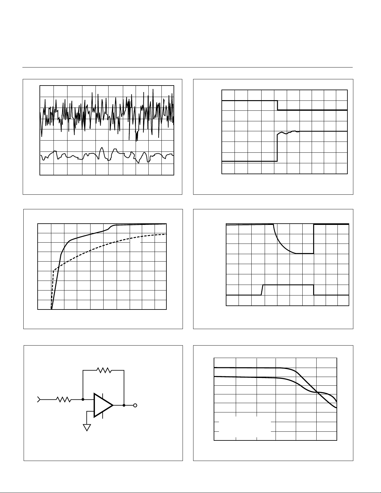
Overload Recovery
The TC901 recovers quickly from output saturation.
Typical recovery time from positive output saturation is 20
msec. Negative output saturation recovery time is typically
msec.
Thermocouple Errors
Heating a junction made from two different metallic
wires causes current flow. This is known as the Seebeck
effect. An open-circuit voltage (Seebeck voltage) can be
measured across the junction. Junction temperature and
metal type determine the magnitude. Typical values are
0.1µV/°C to 10µV/°C. Thermal-induced voltages can be
many times larger than the TC901's offset voltage drift.
Unless unwanted thermocouple potentials can be controlled, system performance will be less than optimum.
Unwanted thermocouple junctions are created when
leads are soldered or sockets/connectors are used. Low
thermoelectric coefficient solder can reduce errors. A 60%
Cd/40% Sn Pb solder has one-tenth the thermal voltage of
common 64% Sn/36% Pb solder at a copper junction.
The number and type of dissimilar metallic junctions in
the input circuit loop should be balanced. If the junctions are
kept at the same temperature, their summation will add to
zero, canceling errors (Figure 7).
Shielding precision analog circuits from air currents —
especially those caused by power dissipating components
and fans — will minimize temperature gradients and minimize thermocouple-induced errors.
Avoiding Latch-Up
Larger voltages can turn the p-n-p-n device on, causing
excessive device power supply current and excessive power
dissipation. TC901's power supply should be established at
the same time (or before) input signals are applied. If this is
not possible, input current should be limited to 100µA to
avoid triggering the p-n-p-n structure.
Pin Compatibility
The CMOS TC901 is pin compatible with other chopperstabilized amplifiers, such as the 7650, 7652 and 1052.
Amplifiers such as the 7650 require 0.1µF external capacitors connected to pins 1 and 8. The TC901 includes the
chopper capacitors on-chip, so external capacitors are not
required. Since pins 1, 5 and 8 of the TC901 are not
connected, the TC901 can directly replace other chopperstabilized amplifiers in existing circuits.
The TC901 pinout also matches many popular bipolar
and JFET op amps, such as the OP-07, OP-20, LM101,
LM108, 356 and 741. In many applications that operate from
±15V power supplies, the TC901 offers superior electrical
performance and is a functional pin-compatible replacement. Offset voltage correction potentiometers, compensation capacitors, and chopper-stabilization capacitors can be
removed when retrofitting existing equipment designs.
System parts count, assembly time, and system cost are
reduced, while reliability and performance are improved.
Overload Recovery
J = J
3
4
J = J
J = J
J
3
J
4
–
J
3
+
+
J
4
–
Figure 7. Unwanted Thermocouple Errors Eliminated by Reducing
Thermal Gradients and Balancing Junctions
© 2001 Microchip Technology Inc. DS21480A
NO TEMPERATURE DIFFERENTIAL
2
5
AND SAME METALLIC CONNECTION
1
6
V
3
V = V + V + V – V – V – V = 0
V
4
J
2
J
5
J
2
+ – + –
V
2
T123456
V
5
+ – + –
J
5
J
1
J
6
J
1
V
1
V
6
J
6
PACKAGE
PIN
V = 0
T
The TSC90X Series recovers quickly from output
saturation. Typical recovery time from positive output saturation is 20msec. Negative output saturation recovery time
is typically 5msec.
3
TC901- 7 9/5/96
TC901
(B) 0.1 TO1.0 Hz (A) 0.1 TO 1.0 Hz
1 µV/DIV 1 µV/DIV
0 1 2 3 4 5 6 7 8
1 sec/DIV
9 10
Dual Auto-Zeroed Operational Amplifiers
2V
INPUT
2 V/DIV
0V
0V
OUTPUT
5 V/DIV
–15V
5 msec/DIV
VOS (µV)
4
6
9
10
12
14
16
18
20
22
0 2 4
Figure 1. Input Voltage Noise
Figure 3. Recovery From Negative Saturation
VDD (µA)
VOS
450
400
350
2V
OUTPUT
5 V/DIV
300
250
0V
200
6 8 10 12 14 16 18 20
150
100
50
0
OUTPUT
5 V/DIV
0V
–2V
20 msec/DIV
±VS (V)
Figure 2. VOS and IDD vs Supply Voltage Figure 4. Recovery From Positive Saturation
R
2
R
1
+15V
–
+
–15V
OUTPUT
GAIN = 40
R
= 1kΩ
1
R
= 40kΩ
2
+50
+40
+30
+20
+10
0
GAIN (dB)
–10
–20
–30
–40
PHASE MARGIN
10kΩ with 50 pF LOAD
36° at 700 kHz at 70°C
40° at 800 kHz at 25°C
0 10 100 1k
10k 100k 1M
FREQUENCY (Hz)
+240
+180
+120
+60
0°C
–120
–180
TC901- 7 9/5/96
Figure 5. Saturation Test Circuit
Figure 6. Phase-Gain
4
© 2001 Microchip Technology Inc. DS21480A

Dual Auto-Zeroed Operational Amplifiers
PACKAGE DIMENSIONS
8-Pin SOIC Narrow
TC901
.050 (1.27) TYP.
.197 (5.00)
.189 (4.80)
.020 (0.51)
.013 (0.33)
.157 (3.99)
.150 (3.81)
.010 (0.25)
.004 (0.10)
.244 (6.20)
.228 (5.79)
.069 (1.75)
.053 (1.35)
8-Pin Plastic Dip
PIN 1
8° MAX.
.010 (0.25)
.007 (0.18)
.050 (1.27)
.016 (0.40)
.045 (1.14)
.030 (0.76)
.200 (5.08)
.140 (3.56)
.150 (3.81)
.115 (2.92)
© 2001 Microchip Technology Inc. DS21480A
.400 (10.16)
.348 (8.84)
.110 (2.79)
.090 (2.29)
.070 (1.78)
.040 (1.02)
.022 (0.56)
.015 (0.38)
.260 (6.60)
.240 (6.10)
.040 (1.02)
.020 (0.51)
.310 (7.87)
.290 (7.37)
.015 (0.38)
.008 (0.20)
.400 (10.16)
.310 (7.87)
5
3° MIN.
Dimensions: inches (mm)
TC901- 7 9/5/96

TC901
Dual Auto-Zeroed Operational Amplifiers
W
ORLDWIDE SALES AND SERVICE
AMERICAS
Corporate Office
2355 West Chandler Blvd.
Chandler, AZ 85224-6199
Tel: 480-792-7200 Fax: 480-792-7277
Technical Support: 480-792-7627
Web Address: http://www.microchip.com
Rocky Mountain
2355 West Chandler Blvd.
Chandler, AZ 85224-6199
Tel: 480-792-7966 Fax: 480-792-7456
Atlanta
500 Sugar Mill Road, Suite 200B
Atlanta, GA 30350
Tel: 770-640-0034 Fax: 770-640-0307
Austin
Analog Product Sales
8303 MoPac Expressway North
Suite A-201
Austin, TX 78759
Tel: 512-345-2030 Fax: 512-345 -60 85
Boston
2 Lan Drive, Suite 120
Westford, MA 01886
Tel: 978-692-3848 Fax: 978-692 -38 21
Boston
Analog Product Sales
Unit A-8-1 Millbrook Tarry Condominium
97 Lowell Road
Concord, MA 01742
Tel: 978-371-6400 Fax: 978-371 -00 50
Chicago
333 Pierce Road, Suite 180
Itasca, IL 60143
Tel: 630-285-0071 Fax: 630-2 85 -00 75
Dallas
4570 Westgrove Drive, Suite 160
Addison, TX 75001
Tel: 972-818-7423 Fax: 972-818 -29 24
Dayton
Two Prestige Place, Suite 130
Miamisburg, OH 45342
Tel: 937-291-1654 Fax: 937-291 -91 75
Detroit
Tri-Atria Office Building
32255 Northwestern Highway , Suite 190
Farmington Hills, MI 48334
Tel: 248-538-2250 Fax: 248-5 38 -22 60
Los Angele s
18201 Von Karman, Suite 1090
Irvine, CA 92612
Tel: 949-263-1888 Fax: 949-263 -13 38
Mountain View
Analog Product Sales
1300 Terra Bella Avenue
Mountain View, CA 94043-1836
Tel: 650-968-9241 Fax: 650-967 -15 90
All rights reserved. © 2001 Microchip T echnology Incorporated. Printed in the USA. 1/01 Printed on recycled paper.
Information contained in this publication regarding device applications and the like is intended through suggestion only and may be superseded by
updates. It is your re sponsib ility to en sure that your applicatio n meets w ith your specifications . No re presen tation or warrant y is given and no liability is
assumed by Micro chip Technology Incorporated with re spec t to the accur acy or use of such infor mation, or infringem ent of paten ts or o the r in te lle ct ua l
property rights arising from such use or otherwise. Use of Microchipí s products as critical components in life support systems is not aut hor ized exce pt w ith
express written approval by Microchip. No licenses are conveyed, implicitly or otherwise, except as maybe explicitly expressed herein, under any intellectual property rights. The Mi crochip logo and name are registered trad emarks of Microchip Technology Inc. in the U.S.A. and other countries. All rights
reserved. All other trademarks mentioned herein are the property of their respective companies.
New York
150 Motor Parkway, Suite 202
Hauppauge, NY 11788
Tel: 631-273-5305 Fax: 631-273-5335
San Jose
Microchip Technology Inc.
2107 North First Street, Suite 590
San Jose, CA 95131
Tel: 408-436-7950 Fax: 408-436-7955
Toronto
6285 Northam Drive, Suite 108
Mississa uga, Ontari o L4V 1X5, Ca nada
Tel: 905-673-0699 Fax: 905-673-6509
ASIA/PACIFIC
China - Beijing
Microchip Technology Beijing Office
Unit 915
New China Hong Kong Manhattan Bldg.
No. 6 Chaoyangmen Beidajie
Beijing, 100027, No. China
Tel: 86-10-85282100 Fax: 86-10-85282104
China - Shanghai
Microchip Technology Shanghai Office
Room 701, Bldg. B
Far East Int ernational Plaza
No. 317 Xian Xia Road
Shanghai, 200051
Tel: 86-21-6275-5700 Fax: 86-21-6275-5060
Hong Kong
Microchip Asia Pacific
RM 2101, Tower 2, Metroplaza
223 Hing Fong Road
Kwai Fong, N.T., Hong Kong
Tel: 852-2401-1200 Fax: 852-2401-3431
India
Microchip Technology Inc.
India Liaison Office
Divyasree Chambers
1 Floor, Wing A (A3/A4)
No. 11, OíShaugnessey Road
Bangalore, 560 025, India
Tel: 91-80-2290061 Fax: 91-80-2290062
Japan
Microchip Technology Intl. Inc.
Benex S-1 6F
3-18-20, Shinyokohama
Kohoku-Ku, Yokohama-shi
Kanagawa, 222-0033, Japan
Tel: 81-45-471- 6166 Fax: 81-45-471-6122
Korea
Microchip Technology Korea
168-1, Youngbo Bldg. 3 Floor
Samsung-Dong, Kangnam-Ku
Seoul, Korea
Tel: 82-2-554-7200 Fax: 82-2-558-5934
ASIA/PACIFIC
(continued)
Singapore
Microchip Technology Singapore Pte Ltd.
200 Middle Road
#07-02 Prime Centre
Singapore, 188980
Tel: 65-334-8870 Fax: 65-334-8850
Taiwan
Microchip Technology Taiwan
11F- 3, No. 207
Tung Hua North Road
Taipei, 105, Taiwan
Tel: 886-2-2717-7175 Fax: 886-2-2545-0139
EUROPE
Australia
Microchip Technology Australia Pty Ltd
Suite 22, 41 Rawson Street
Epping 2121, NSW
Australia
Tel: 61-2-9868-6733 Fax: 61-2-9868-6755
Denmark
Microchip Technology Denmark ApS
Regus Business Centre
Lautrup hoj 1-3
Ballerup D K-2750 Denmark
Tel: 45 4420 9895 Fax: 45 4420 9910
France
Arizona Microchip Technology SARL
Parc díActivite du Moulin de Massy
43 Rue du Saule Trapu
Batiment A - ler Etage
91300 Massy, France
Tel: 33-1-69-53-63-20 Fax: 33-1-69-30-90 -79
Germany
Arizona Microchip Technology GmbH
Gustav-Heinemann Ring 125
D-81739 Munich, Germany
Tel: 49-89-627-144 0 Fax: 49-89-627-144-44
Germany
Analog Product Sales
Lochhamer Strasse 13
D-82152 Martinsried, Germany
Tel: 49-89-895650-0 Fax: 49-89-895650-22
Italy
Arizona Microchip Technology SRL
Centro Direzionale Colleoni
Palazzo Taurus 1 V. Le Colleoni 1
20041 Agrate Brianza
Milan, Italy
Tel: 39-039-65791-1 Fax: 39-039-6899883
United Kingdom
Arizona Microchip Technology Ltd.
505 Eskdale Road
Winnersh Triangle
Wokingham
Berkshire, England RG41 5TU
Tel: 44 118 921 5869 Fax: 44-118 921-5820
01/09/01
TC901- 7 9/5/96
6
© 2001 Microchip Technology Inc. DS21480A
 Loading...