

TC850
15-Bit, Fast Integrating CMOS A/D Converter
Features
• 15-bit Resolution Plus Sign Bit
• Up to 40 Conversions per Second
• IntegratingADC Technique
- Monotonic
- High Noise Immunity
- Auto Zeroed Amplifiers Eliminate Offset
Trimming
• Wide Dynamic Range: 96dB
• Low Input Bias Current: 30pA
• Low Input Noise: 30µV
P-P
• Sensitivity: 100µV
• Flexible Operational Control
• Continuous or On Demand Conversions
• Data Valid Output
• Bus Compatible, 3-State Data Outputs
-8-BitDataBus
-SimpleµP Interface
- Two Chip Enables
- Read ADC Result Like Memory
• ± 5V Power Supply Operation: 20mΩ
• 40-Pin Dual-in-Line or 44-Pin PLCC Packages
Applications
• Precision Analog Signal Processor
• PrecisionSensor Interface
• High Accuracy DC Measurements
Device Selection Table
Part Number Package
TC850CPL 40-Pin PDIP 0°Cto+70°C
TC850IJL 40-Pin CERDIP -25°Cto+85°C
TC850CLW 44-Pin PLCC 0°Cto+70°C
TC850ILW 44-Pin PLCC -25°Cto+85°C
Temperature
Range
Package Types
CS
CE
WR
RD
CONT/DEMAND
OVR/POL
L/H
DB7
DB6
DB5
DB4
DB3
DB2
DB1
DB0
BUSY
OSC
OSC
TEST
DGND
CONT/DEMAND
RD
6543 1442
OVR/POL
7
8
L/H
9
DB7
10
DB6
11
DB5
12
NC
13
DB4
DB3
DB2
DB1
DB0
18 19 20 21 23 24
BUSY
1
OSC
NC = No Internal Connection
40-Pin PDIP/CERDIP
1
2
3
4
5
6
7
TC850CPL
8
TC850IJL
9
10
11
12
13
14
15
16
17
1
18
2
19
20
44-Pin PLCC
WR
CE
CS
NC
VDDREF
43 42 41 40
TC850CLW
TC850ILW
DGND
25 26 27 28
NC
COMP
2
OSC
22
TEST
40
V
DD
REF1+
39
38
37
36
35
34
33
32
31
30
29
28
27
26
25
24
23
22
21
+
+
1
REF1
C
SS
OUT
V
INT
C
REF1
C
REF1
REF-
C
REF2
C
REF2
REF
+
2
IN+
INANALOG
COMMON
C
INTB
C
INTA
C
BUFA
C
BUFB
BUFFER
INT
IN
INT
OUT
V
SS
COMP
-
REF1
C
REF-
39
38
37
36
35
34
33
3214
3115
3016
2917
IN
INT
BUFFER
+
-
-
+
C
REF2
C
REF2
REF
IN+
IN-
NC
ANALOG
COMMON
C
INTB
C
INTA
C
BUFA
C
BUFB
-
+
+
2
2002 Microchip TechnologyInc. DS21479B-page 1
TC850
General Description
The TC850 is a monolithic CMOS A/D converter (ADC)
with resolution of 15-bitsplus sign. It combines a chopper-stabilized buffer and i ntegrator with a unique multiple-slope integration technique that increases
conversion speed. The result is 16 times improvement
in speed over previous 15-bit, monolithic integrating
ADCs (from 2.5 conversions per second up to 40 per
second). Faster conversion speed is especially welcome in systems with human interface, such as digital
scales.
The TC850 incorporates an ADC and a µP-compatible
digital interface. Only a voltage reference and a few,
noncritical, passive components are required to form a
complete 15-bit plus sign ADC. CMOS processing provides the TC850 with high-impedance, differential
inputs. Input bias current is typically only 30pA, permitting direct interface to sensors. Input sensitivity of
100µV per least significant bit (LSB) eliminates the
Functional Block Diagram
Pinout of 40-Pin Package
REF2+
+
REF
REF-
1
BUF
R
INT
INT IN
need for precision external amplifiers. The internal
amplifiers are auto zeroed, ensuring a zero digital output, with 0V analog input. Zero adjustment
potentiometers or calibrations are not required.
The TC850 outputsdataonan8-bit,3-statebus.Digital
inputs are CMOS compatible while outputs are TTL/
CMOS compatible.Chip-enable and byte-selectinputs,
combined with an end-of-conversion output, ensures
easy interfacing to a wide variety of microprocessors.
Conversions can be performed continuously or on
command. In continuous mode, data is read as three
consecutivebytes and manipulation of address lines i s
not required.
Operating from ±5V supplies, the TC850 dissipates
only 20mΩ. The TC850 i s packaged in a 40-pin plastic
or ceramic dual-in-line package (DIPs) and in a 44-pin
plastic leaded chip carrier (PLCC), surface-mount
package.
C
INT
INT OUT
+5V–5V
IN+
IN-
COMMON
-
32
31
30
Analog
Mux
A/D
Control
Sequencer
Clock
Oscillator
17 7
OSC
1
18
OSC
+
Buffer
÷4
53
CONT/
2
DEMAND
L/H6OVR/
POL
-
+
Integrator
TC850
Bus Interface
Decode Logic
4RD1CS2
WR
232425363439
CE
22 40
Comparator
+
-
6-Bit
Up/Down
Counter
Data Latch
Octal 2-Input Mux
3-State Data Bus
15 8
DB0
9-Bit
Up/Down
Counter
. . . .
DB7
DS21479B-page 2
2002 Microchip TechnologyInc.
TC850
1.0 ELECTRICAL SPECIFICATIONS
Absolute Maximum Ratings*
Positive Supply Voltage..........................................+6V
Negative Supply Voltage.......................................- 9V
Analog Input Voltage (IN+ pr IN-).............. V
DD
to V
SS
*Stresses above those listed under "Absolute Maximum Ratings"maycause permanentdamage to thedevice.These are
stress ratings only and functional operation of the device at
these or any other conditions above those indicated in the
operation sections of the specifications is not implied. E xposure to Absolute Maximum R ating conditions for extended
periodsmay affectdevice reliability.
Voltage Reference Input:
(REF
+, REF1–, REF2+).................. VDDto V
1
SS
Logic Input Voltage.............VDD+0.3VtoGND–0.3V
Current Into Any Pin............................................10mA
While Operating ......................................100µA
Ambient Operating Temperature Range
C Device.......................................0°C to +70°C
I Device......................................-25°C to +85°C
Package Power Dissipation (T
≤ 70°C)
A
CerDIP .....................................................2.29Ω
Plastic DIP................................................1.23Ω
Plastic PLCC ...........................................1.23Ω
TC850 ELECTRICAL SPECIFICATIONS
Electrical Characteristics: VS=±5V;F
Symbol Parameter Min Typ Max Unit Test Conditions
ZeroScaleError ±0.25 ±0.5 LSB V
End PointLinearity Error — ±1 ±2 LSB -V
Differential Nonlinearity — ±0.1 ±0.5 LSB
InputLeakage Current — 30 75 pA VIN=0V,TA=25°C
I
IN
V
CommonMode Voltage Range VSS+1.5 — VSS– 1.5 V Over OperatingTemperatureRange
CMR
CMRR Common M ode Rejection Ratio — 80 — dB V
Full Scale Gain Temperature
Coefficient
Zero Scale Error
Temperature Coefficient
Full Scale Magnitude
Symmetry Error
InputNoise — 30 — µV
e
N
+ Positive Supply Current — 2 3.5 mA
I
S
– Negative Supply Current — 2 3.5 mA
I
S
Output High Voltage 3.5 4.9 — V IO=500µA
V
OH
Output Low Voltage — 0.15 0.4 V IO=1.6mA
V
OL
Output Leakage Current — 0.1 1 µA Pins 8 -15, High-Impedance State
I
OP
InputHighVoltage 3.5 2.3 — V Note 3
V
IH
Input Low Voltage — 2.1 1 V Note 3
V
IL
Input Pull-Up Current — 4 — µA Pins2,3,4,6,7;VIN=0V
I
PU
InputPull-Down Current — 14 — µA Pins1,5;VIN=5V
I
PD
I
C
Oscillator OutputCurrent — 140 — µAPin18,V
OSC
InputCapacitance — 1 — pF Pins 1 - 7, 17
C
IN
Output Capacitance — 15 — pF Pins 8 -15, High-Impedance State
OUT
Note 1: Demand mode, CONT/DEMAND
2: Continuous mode, CONT/DEMAND
3: Digital inputs have CMOS logic levels and internal pull-up/pull-down resistors. For TTL compatibility, external pull-up
resistors to V
are recommended.
DD
= 61.44kHz,VFS= 3.2768V, TA= 25°C, Figure 1-1, unless otherwise specified.
CLK
=0V
IN
≤ VIN≤ +V
FS
—1.13 nA-25°≤ T
=0V,VCM=±1V
IN
≤ +85°C
A
FS
— 2 5 ppm/°C External Ref. Temperature
Coefficient = 0 ppm/°C
=0V
IN
= ±3.275V
IN
≤ +70°C
A
≤ +70°C
A
OUT
=2.5V
0°C ≤ T
—0.32
µV/°C V
0°C ≤ T
—0.52LSBV
Not Exceeded 95% of Time
P-P
= LOW. Figure 8-5 timing diagram. CL= 100pF.
= HIGH. Figure 8-7 timing diagram.
2002 Microchip TechnologyInc. DS21479B-page 3
TC850
TC850 ELECTRICAL SPECIFICATIONS (CONTINUED)
Electrical Characteristics: VS=±5V;F
Symbol Parameter Min Typ Max Unit Test Conditions
T
Chip-Enable Access Time — 230 450 nsec CS or CE,RD=LOW(Note1)
CE
Read-Enable Access Time — 190 450 nsec CS = HIGH, CE =LOW,(Note1)
T
RE
T
T
Data Hold From CS or CE —250450nsecRD=LOW,(Note1)
DHC
Data Hold From RD —210450nsecCS=HIGH,CE=LOW,(Note1)
DHR
OVR/POL Data Access Time — 140 300 nsec CS = HIGH, CE =LOW,
T
OP
Low/High Byte Access Time — 140 300 nsec CS = HIGH, CE =LOW,
T
LH
ClockSetupTime 100 — — nsec Positive or NegativePulse Width
T
T
T
RD Minimum Pulse Width 450 230 — nsec CS= HIGH, CE =LOW,(Note2)
WRE
RD Minimum Delay Time 150 50 — nsec CS = HIGH, CE =LOW,(Note2)
WRD
WR Minimum Pulse Width 75 25 — nsec CS = HIGH, CE =LOW,(Note1)
WWD
Note 1: Demand mode, CONT/DEMAND
2: Continuous mode, CONT/DEMAND
3: Digital inputs have CMOS logic levels and internal pull-up/pull-down resistors. For TTL compatibility, external pull-up
resistors to V
are recommended.
DD
= 61.44kHz,VFS= 3.2768V, TA= 25°C, Figure 1-1, unless otherwise specified.
CLK
RD
=LOW,(Note1)
RD = LOW, (Note 1)
= LOW. Figure 8-5 timing diagram. CL= 100pF.
= HIGH. Figure 8-7 timing diagram.
DS21479B-page 4
2002 Microchip TechnologyInc.
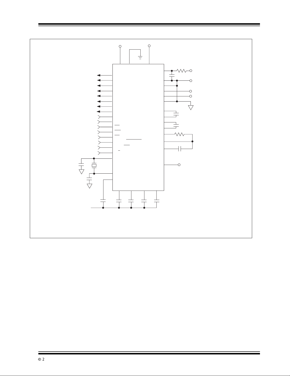
FIGURE 1-1: STANDARD TEST CIRCUIT CONFIGURATION
TC850
+5V
20
V
DGND
DD
16
BUSY
8
DB7
9
DB6
10
11
12
13
14
15
1
2
3
4
5
6
7
17
18
21
0.1
µF
OSC
OSC
COMP
C
**
61.44 kHz
**
ANALOG COMMON
DB5
DB4
DB3
DB2
DB1
DB0
CS
CE
WR
RD
CONT/DEMAND
OVR/POL
L/H
TC850
1
2
C
INTBCBUFACBUFB
INTA
28 2729
0.1
µF
0.1
µF
-5V
2240
V
SS
REF
REF
REF-
C
REF1
C
REF1
C
REF2
C
REF2
BUFFER
INT
INT
OUT
TEST
0.1
µF
IN+
IN-
1
2
IN
26
+
+
+
+
-
0.1
µF
32
31
30
39
33
36
38
37
34
35
120MkΩ
25
24
23
19
100MΩ
0.01µF Input
+1.6384V
+0.0256V
*
1µF
*
1µF
R
INT
0.1µF
C
INT
NC
NOTES: Unless otherwise specified, all 0.1µF capacitors are film dielectric.
Ceramic capacitors are not recommended.
NC = No Connection
*Polypropylene capacitors.
** 100pF Mica capacitors.
2002 Microchip TechnologyInc. DS21479B-page 5
TC850
2.0 PIN DESCRIPTIONS
The descriptions of the pins are listed in Table .
TABLE 2-1: PIN FUNCTION TABLE
Pin Number
(40-Pin
PDIP/CERDIP)
1 2 CS Chip select, active HIGH. Logically ANDed, with CE
23CE
34WR
45RD
5 6 CONT/
67OVR/POL
78L/H
8 9 DB7 Most significant data bit output. When reading the A/D conversionresult, the
9-15 10-17 DB6-DB0 Data outputs DB6-DB0. 3-state, bus compatible.
16 18 BUSY A/D conversion status output. BUSY goes to a logic HIGH at the beginning of the
17 19 OSC
18 20 OSC
19 21 TEST For factory testing purposes only. Do not make external connectionto this pin.
20 22 DGND Digital groundconnection.
21 24 COMP Connection for comparator auto zero capacitor. Bypass to V
22 25 V
23 26 INT
24 27 INT
25 28 BUFFER Output of the input buffer.Connect to R
26 29 C
27 30 C
28 31 C
29 32 C
30 33 ANALOG
31 35 IN– Negative differential analog input.
32 36 I N+ Positive differentialanalog input.
Note 1: This pin incorporates a pull-down resistortoDGND.
2: This pin incorporatesa pull-upresistor to V
3: Pins 1, 23 and 34 (44-PLCC) package are NC “No Internal connection.
Pin Number
(44-Pin PLCC)
Symbol Description
inputs (Note 1).
Chip enable, active LOW (Note 2).
Writeinput,activeLOW.Whenchipisselected(CS=HIGHandCE= LOW) and
in demand mode (CONT/DEMAND
conversion (Note 1).
Read input,active LOW. When CS = HIGH and CE = LOW, a logic LOW on RD
enables the 3-state data outputs(Note 2).
Conversion control input. When CONT/DEMAND = LOW, conversionsareiniti-
DEMAND
ated by the WR
performed continuously (Note 1).
Overrange/polarity data-select input.Whenmakingconversionsin the demand
mode (CONT/DEMAND
whenthehigh-orderbyteisactive(Note2).
Low/high byte-select input. When CONT/DEMAND = LOW, this input controls
whetherlow-byte or high-byte data is enabled on DB0 through DB7 (Note 2).
polarity, overrange and DB7 data are output on this pin.
de-integratephase,thengoesLOWwhen conversion is complete.The falling
edge of BUSY can be used to generate a
Crystal oscillatorconnection or externaloscillator input.
1
Crystal oscillator connection.
2
SS
BUFB
BUFA
INTA
INTB
Negative power supply connection, typically -5V.
Outputof the integrator amplifier.Connect to C
OUT
Input to the integrator amplifier. Connect to summing node of R
IN
Connection for buffer auto zero capacitor. Bypass to VSSwith 0.1µF.
Connection to buffer auto zero capacitor. Bypass to VSSwith 0.1µF.
Connection for integrator auto zero capacitor. Bypass to VSSwith 0.1µF.
Connection for integrator auto zero capacitor. Bypass to VSSwith 0.1µF.
Analog common.
COMMON
.
DD
to enable read and write
=LOW),alogicLOWonWRstartsa
input. When CONT/DEMAND = HIGH, conversions are
= LOW), OVR/POL controlsthedataoutputonDB7
µP interrupt.
SS
.
INT
.
INT
with 0.1µF.
and C
INT
INT
.
DS21479B-page 6
2002 Microchip TechnologyInc.
TABLE 2-1: PIN FUNCTION TABLE (CONTINUED)
Pin Number
(40-Pin
PDIP/CERDIP)
33 37 REF2+ Positiveinputfor reference voltage V
34 38 C
35 39 C
36 40 REF– Negative input for reference voltages.
37 41 C
38 42 C
39 43 REF
40 44 V
Note 1: This pin incorporates a pull-down resistortoDGND.
2: This pin incorporatesa pull-upresistor to V
3: Pins 1, 23 and 34 (44-PLCC) package are NC “No Internal connection.
Pin Number
(44-Pin PLCC)
Symbol Description
+ Positive connection for V
REF2
– Negative connection for V
REF2
– Negative connection for V
REF1
+ Positive connection for V
REF1
+ Positiveinputfor V
1
DD
Positive power supply connection, typically +5V.
.
DD
REF1
reference capacitor.
REF2
reference capacitor.
REF2
reference capacitor.
REF1
reference capacitor.
REF1
.
REF2
.(V
REF2=VREF1
TC850
/64)
2002 Microchip TechnologyInc. DS21479B-page 7
TC850
3.0 DETAILED DESCRIPTION
The TC850 is a multiple-slope, integrating A/D converter ( ADC). The multiple-slope conversion process,
combined with chopper-stabilized amplifiers, results in
a significant increase in ADC speed, while maintaining
very high resolution and accuracy.
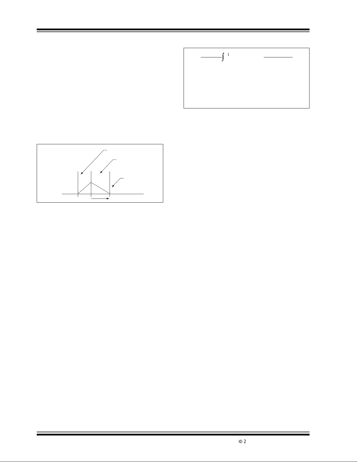
3.1 Dual Slope Conversion P rinciples
The conventional dual slope converter measurement
cycle (shown in Figure 3-1) has two distinct phases:
1. Input signal integration
2. Reference voltage integration (de-integration).
FIGURE 3-1: DUAL SLOPE ADC CYCLE
Signal De-integrate
Reference
De-integrate
End of Conversion
Integrator
Output
The input signal being converted is integrated for a
fixed time period, measured by counting clock pulses.
An opposite polarity constant reference voltage is then
de-integrateduntil the integrator output voltage returns
to zero. The reference integration time is directly
proportionalto the input signal.
In a simple dual slope converter, complete conversion
requires the i ntegrator output to "ramp-up" and "rampdown." Most dual slope converters add a third phase,
auto zero. During auto zero, offset voltages of the input
buffer, integrator and comparator are nulled, thereby
eliminating the need for zero offset adjustments.
Dual slope converter accuracy is unrelated t o the integrating resistor and capacitor values, as long as they
are stable during a measurement cycle. By converting
the unknown analog input voltage into an easily measured function of time, the dual slope converter
reduces the need for expensive, precision passive
components.
Noise immunity is an inherent benefit of the integrating
conversion method. Noise spikes are integrated, or
averaged, to zero during the integration period. I ntegrating ADCs are immune to t he large conversion
errors that plague successive approximation
converters in high-noise environments.
A simple mathematical equation relates the input signal, reference voltage and integration time:
Auto
Zero
Time
0V
EQUATION 3-1:
where:
1
R
INTCINT
V
REF
T
INT
T
DEINT
T
INT
VIN(T)DT =
∫
0
= Reference voltage
= Signal integration time (fixed)
= Reference voltage integration time
(variable).
V
REFTDEINT
R
INTCINT
3.2 Multiple Slope Conversion
Principles
One limitation of the dual slope measurement technique is conversion speed. In a typical dual slope
method, the auto zero and integrate times are each
one-half of the de-integrate time. For a 15-bit conver-
14+214+215
sion,2
for auto zero, integrate and de-integrate phases,
respectively. The large number of clock cycles effectively limits the conversion rate to about 2.5 conversions per second, when a typical analog CMOS
fabricationprocess is used.
The TC850 uses a multiple slope conversiontechnique
to increase conversion speed ( Figure 3-2). This technique m akes use of a two-slope de-integration phase
and permits 15-bit resolution up to 40 conversions per
second.
During the TC850's de-integration phase, the integration capacitor is rapidly dischargedto yield a resolution
of 9 bits. At this point, some charge will remain on the
capacitor. This remaining charge is then slowly deintegrated, producing an additional 6 bits of resolution.
The result is 15 bits of resolution achieved with only
9+26
2
(512 + 64, or 576) clock pulses for deintegration.A complete conversioncycle occupies only
1280 clock pulses.
In order to generate "fast-slow" de-integration phases,
two voltage references are required. The primary reference (V
(typically V
) is set to one-half of the full scale voltage
REF1
REF1
secondaryvoltagereference (V
(typically 25.6 mV). To maintain 15-bit linearity, a tolerance of 0.5% for V
(65,536)clockpulsesare required
= 1.6384V, and VFS= 3.2768V). The
is recommended.
REF2
)issettoV
REF2
REF1
/64
DS21479B-page 8
2002 Microchip TechnologyInc.

TC850
p
FIGURE 3-2: “FAST S LOW”
REFERENCE DE-
4.0 ANALOG SECTION
DESCRIPTION
INTEGRATION CYCLE
The TC850 analog section consists of an input buffer
amplifier, integrator amplifier, comparator and analog
switches. A simplified block diagram is shown in
Figure 4-1.
Signal Integrate
"Fast" Reference
De-integrate
(9-Bit Resolution)
"Slow" Reference De-integrate
(6-Bit Resolution)
4.1 Conversion Timing
End of Conversion
Auto
Integrator
Output
Zero
0V
Time
FIGURE 4-1: ANALOG SECTION SIMPLIFIED SCHEMATIC
C
REF2
-
REF2+
-
DE1
(-)
IN+
C
REF1
INT
C
REF1
DE
DE1
(+)
REF1-
C
REF2
C
REF1
DE DE
REF1+
+
DE
DE1
(-)
Each conversion consists of three phases:
1. Zero Integrator
2. Signal Integrate
3. Reference Integrate (or De-integrate)
Each conversion cycle requires 1280 internal clock
cycles (Figure 4-2).
-
DE1
(+)
C
REF2
BUFF
-
+
Buffer*
INT
C
INT
IN
Integrator*
–
+
INT
OUT
–
+
Comparator*
To Digital
Section
R
INT
ANALOG
COMMON
IN-
*Auto Zeroed Am
INT
lifiers
DE1
(+)
INT
DE1
(-)
FIGURE 4-2: CONVERSION TIMING
Internal
Clock
Conversion
Phase
. . . . . . .
246 256 778
Zero Integrator Reference Integrate
DE2
(+)
1280 Clock Cyles
Signal Integrate
DE2
(-)
Z1
TC850
. . . . . . . . . . . . . .
2002 Microchip TechnologyInc. DS21479B-page 9

TC850
4.2 Zero Integrator Phase
During the zero integrator phase, the differential input
signalis disconnected from the circuit by openinginternal analog gates. The internal nodes are shorted to
analog common (ground) t o establish a zero input condition. At the same time, a feedback loop is closed
around the input buffer, integrator and comparator.The
feedback loop ensures the integrator output is near 0V
before the signal integrate phase begins.
During this phase, a chopper-stabilization technique i s
used t o cancel offset errors in the input buffer, integrator and comparator. Error voltages are stored on the
C
BUFF,CINT
phase requires 246 clock cycles.
and COMP capacitors. The zero integrate
4.3 Signal Integrate Phase
The z ero integrator loop is opened and the internal differentialinputs are connectedtoIN
ential input signal is i ntegrated for a fixed time period.
The TC850 signal integrateperiodis256 clock periods,
or counts. The crystal oscillator frequency is ÷4 before
clocking the internal counters.
The i ntegration t ime period is:
EQUATION 4-1:
INT
=
4 x 256
F
T
+ and IN-. The differ-
OSC
4.4 Reference Integrate Phase
Duringreferenceintegratephase,the charge stored on
the integrator capacitor is discharged. The time
required to discharge the capacitor is proportional to
the analog input voltage.
The referenceintegratephase is dividedintothreesubphases:
1. Fast
2. Slow
3. Overrange de-integrate
During fast de-integrate, V
analog common and V
viously-chargedreferencecapacitor (C
gratorcapacitoris rapidly dischargedfor a maximumof
512 internal clock pulses, yielding 9 bits of resolution.
During the slow de-integrate phase, the internal V
node i s now connected to the C
residual charge on the integrator capacitor is further
dischargeda maximumof 64clock pulses.Atthispoint,
the analog input voltage has been converted with 15
bits of resolution.
If the analog input is greater than full scale, the TC850
performs up to three overrange de-integrate subphases. Each subphase occupies a maximum of 64
clock pulses. The overrange feature permits analog
inputs up to 192 LSBs greater than full scale to be correctly converted. This feature permits t he user to digitallynullup to 192 counts of input offset, while retaining
full 15-bit resolution.
In addition to 512 counts of fast, 64 counts of slow and
192 counts of overrange de-integrate, t he reference
integrate phase uses 10 clock pulses to permit internal
nodes to settle. Therefore, the reference integrate
cycle occupies 778 clock pulses.
- is internally connected to
IN
+ is connected across the pre-
IN
REF2
). The inte-
REF1
capacitorand the
IN
+
DS21479B-page 10
2002 Microchip TechnologyInc.

5.0 PIN DESCRIPTION (ANALOG)
5.1 Differential Inputs (IN+ and IN–)
The analog signal to be measured is applied at the IN+
and I N– inputs. The differential input voltage must be
within the Common mode range of the converter. The
input Common mode range extends from V
V
+1.5V. Within this Common mode voltage range,
SS
an 80 dB CMRR is typical.
The integrator output also follows the Common mode
voltage. The integrator output must not be allowed to
saturate. A worst-case condition exists, for example,
when a large, positive Common mode voltage, with a
near full scale negative differential input voltage, is
applied. The negative input signal drives the integrator
positive when most of its available s wing has been
used up by the positive Common mode voltage. For
applications where maximum Common mode range is
critical,integrator swing can be reduced.Theintegrator
output can swing within 0.4V of either supply without
loss of linearity.
-1.5Vto
DD
TC850
5.2 Differential Reference (V
The TC850 requires two reference voltage sources in
order to generate the "fast-slow" de-integrate phases.
The main voltage reference (V
the REF
(V
The reference voltage inputs are fully differential and
the reference voltage can be generated anywhere
within the power supply voltage of the converter. However, to minimize rollover error, especially at high conversion rates, keep the reference Common mode
voltage (i.e., REF-) near or at the analog common
potential. All voltage reference inputs ar e high impedance. Average reference input current is typically only
30pA.
+ and REF- pins. The secondary reference
1
) is applied between the REF2+ and REF- pins.
REF2
) is applied between
REF1
REF
)
5.3 Analog Com mon (ANALOG
COMMON)
Analog common is used as the IN- return during the
zero integrator and de-integrate phases of each conversion. If IN- is at a different potential than analog
common, a Common mode voltage exists in the system. This signal is rejected by the 80dB CMRR of the
converter.However,inmostapplications,IN- will be set
at a fixed, known voltage (power supply common, for
instance). In this case, analog common should be tied
to the same point so t hat the Common mode voltageis
eliminated.
2002 Microchip TechnologyInc. DS21479B-page 11

TC850
6.0 DIGITAL SECTION
DESCRIPTION
The TC850 digital section consists of two sets of conversion counters, control and sequencing logic, clock
oscillator and divider, data latches and an 8-bit, 3-state
interface bus. A simplified schematic of the bus interfacelogicisshowninFigure6-1
6.1 Clock Oscillator
The TC850 includes a crystaloscillatoron-chip.Allthat
is required is to connect a crystal across OSC
OSC
pins and to add two inexpensive capacitors
2
and
1
(Figure 1-1). The oscillator output is ÷ 4 prior to clocking the A/D i nternal counters. For example, a 100kHz
crystal produces a system clock frequency of 25kHz.
Since each conversion requires 1280 clock periods, i n
this case the conversion rate will be 25,000/1280, or
19.5 conversionsper second.
In most applications, however, an external clock is
divided down from the microprocessor clock. In this
case, the OSC
input and OSC
driver should swing from digital ground to V
function is active f or both external clock and crystal
oscillatoroperations.
FIGURE 6-1: BUS INTERFACE SIMPLIFIED S CHEMAT IC
8
DBO–DB7
L/H
RD
CE
CS
POL/OVR
3-State
Buffer
8
Output
Enable
Octal
2-Input Mux
8 7
Select
TC850
pin is used as the external oscillator
1
is left unconnected. The external clock
2
Low-Byte
Up/Down
Counter
High-Byte
Up/Down
Counter
.The÷4
DD
To A/D
Control Logic
WR
CONT/
DEMAND
6.2 Digital Operating Modes
Two modes of operation are available with the TC850,
continuous conversions and on-demand. The operating mode is controlled by the CONT/DEMAND
The bus interface method is different for continuous
and demand modes of operation.
6.2.1 DEMAND MODE OPERATION
When CONT/DEMAND is low,theTC850 performsone
conversion each time the chip is selected and the WR
input is pulsed low. Data is valid on the falling edge of
the BUSY output and can be accessed using the interface truth table (Table 6-1).
6.2.2 CONTINUOUS MODE OPERATION
input.
Select
2-Input Mux
Start
Conversion
End of Conversion
Thelow/high(L/H
(OVR/POL
) inputs are disabled during continuous
Polarity
Overrange
) byte-select and overrange/polarity
mode operation. Data must be read in three consecutive bytes, as shown in Table 6-1.
Note: In continuous mode, the conversion resultmust
be read within 443-1/2 clock cycles of the BUSY
output falling edge. After this time (i.e.,1/2 clock
cycle before BUSY goes high) the internal
counters are reset and the data is lost.
When CONT/DEMAND is high, the TC850 continuously performs conversions. Data will be valid on the
falling edge of the BUSY output and remains valid for
443-1/2 clock cycles.
DS21479B-page 12
2002 Microchip TechnologyInc.

TABLE 6-1: BUS INTERFACE TRUTH TABLE
TC850
CE •CS
Pins 1 and 2
0 0 0 0 0 "1" = Input Positive Data Bits14 - 8
0 0 0 0 1 "1" = Input Overrange
0 0 0 1 X Data Bit 7 Data Bits 6 - 0
00 1 XX Note3
0 1 X X X High-Impedance State
1 X X X X High-Impedance State
Note 1: Pinnumbersreferto40-pinPDIP.
2: Extended overrangeoperation:Although rated at 15 bits (±32,767counts) of resolution, the TC850provides an addi-
tional 191 counts above full scale. For example, with a full-scale input of 3.2768V, the maximum analog input voltage
which will be properly converted is 3.2958V. The extended resolution is signified by the overrange bit being high and the
low-order byte contentsbeing between 0 and 190. For example,witha full-scale voltageof 3.2768V:
3: Continuous mode data transfer:
RD
Pin 4
V
IN
3.2767V Low 255
3.2768V High 000
3.2769V High 001
3.2867V High 099
a. In continuous mode, data MUST be read in three sequential bytes after the BUSY output goes low:
(1) The first byte read will be the high-order byte,with DB7 = polarity.
(2) The second byte read will contain the low-order byte.
(3) The third byte read will again be the high-orderbyte,butwithDB7= overrange.
b. All three data bytes must be read within 443-1/2clock cycles after the fallingedge of BUSY.
c. The c
However, the CS and CE
CONT/DEMAND
Pin 5
Overrange Bit Low Byte Data Bits 14–8
inputmustgohighafter each byte is read, so that the internalbyte counter will be incremented.
inputs can remain enabled through the entire data transfer sequence.
L/H
Pin 7
OVR/POL
Pin 6
10
10
10
10
127
0
0
0
10
10
10
10
DB7
Pin 8
(Note 2)
Pin 9-Pin 15 (Note 1)
Data Bits 14 - 8
DB6–DB0
2002 Microchip TechnologyInc. DS21479B-page 13

TC850
6.3 Pin De scription (Digital)
6.3.1 CHIP SELECT AND CHIP ENABLE
(CS AND CE
The CS and CE inputs permit easy interfacingto a variety of digital bus systems. CE
is active HIGH. These inputs are logically ANDed
internally and are used to enable the RD
inputs.
6.3.2 WRITE ENABLE INPUT (WR)
The write inputis used to initiate a conversion when the
TC850 is in demand mode. CS and CE
for the WR
databus is meaningless during the WR
no data is actually written into the TC850.
input to be recognized. The status of the
6.3.3 READ ENABLE INPUT (RD)
The read input, combined with CS and CE, enable the
3-statedatabus outputs.Also,in continuous mode, the
rising edge of the RD
counter to sequentially read the three data bytes.
6.3.4 LOW/HIGH BYTE SELECT (L/H)
The L/H input determines whet her the l ow (least significant) byte or high (most significant) byte of data is
placedon the 3-statedatabus. This input is meaningful
only when the TC850 is in the demand mode. In the
continuous mode, data must be read in three
predeterminedbytes, so the L/H
)
is active LOW while CS
and WR
must be active
pulse,because
input activates an internal byte
input is ignored.
6.3.6 CONTINUOUS/DEMAND M ODE
INPUT (CONT/DEMAND)
This input controls the TC850 operating mode. When
CONT/DEMAND
sions continuously. In continuous mode, data m ust be
read in the prescribed sequence shown in Table 6-1.
Also, all three data bytes must be read within 443-1/2
internal clock cycles after the BUSY output goes low.
After 443-1/2 clock cycles data will be lost.
When CONT/DEMAND
conversioneach time CS and CE
being pulsed LOW. The conversion is complete and
datacan be read after the falling edge of theBUSY output.Indemandmode,datacanbereadinany
sequence and remains valid until WR
LOW.
is HIGH, the TC850 performs conver-
is LOW, the TC850 begins a
are active and WR is
is again pulsed
6.3.7 BUSY OUTPUT (BUSY)
The BUSY output i s used to convey an end-of-conversion to external logic. BUSY goes HIGH at the beginning of the de-integrate phase and goes LOW at the
end of the conversion cycle. Data is valid on the falling
edge of BUSY. The output-high period is fixed at 836
clock periods, regardless of t he analog input value.
BUSY is active during continuous and demand mode
operation.
This output can also be used to generate an end-ofconversion i nterrupt in µP-based systems.
Noninterrupt-driven systems can poll BUSY to determine when data is valid.
6.3.5 OVERRANGE/POLARITY BIT
SELECT (OVR/POL
The TC850 provides 15 bits of resolution, plus polarity
and overrangebits. Thus,17 bitsofinformation must be
transferredonan8-bitdatabus.Toaccomplishthis,the
overrangeand polaritybits are multiplexedontodatabit
DB7 of the most significant byte. When OVR/POL
HIGH,DB7ofthehighbytecontainstheoverrangestatus(HIGH=analoginputoverrange,LOW=inputwithin
full scale). When OVR/POL
positive analog input polarity and LOW for negative
polarity. The OVR/POL
CS, CE
most significant byte is selected). OVR/POL
when the TC850 is in continuous mode.
and RD are active, and L/H is LOW (i.e., the
input is meaningful only when
)
is
is LOW, DB7 is HIGH for
is ignored
DS21479B-page 14
2002 Microchip TechnologyInc.

TC850
7.0 ANALOG SECTION TYPICAL
APPLICATIONS
7.1 Component S election
7.1.1 REFERENCE VOLTAGE
The typical value for reference voltage V
1.6384V. This value yields a full scale voltage of
3.2768V and resolution of 100µV per step. The V
value is derived by dividing V
V
value is 1.6384V/64, or 25.6mV. The V
REF2
by 64. Thus, typical
REF1
value should be adjusted within ±1% to maintain15-bit
accuracy for the total conversion process;
EQUATION 7-1: :
±1%
V
V
REF
REF1
=
64
The referencevoltageisnotlimitedtoexactly1.6384V,
however, because the TC850 performs a ratiometric
conversion. Therefore, the conversion result will be:
EQUATION 7-2:
V
Digital Counts = • 16384
The full scale voltage can range from 3.2V to 3.5V. Full
scale voltages of less than 3.2V will result in increased
noise in the least significant bits, while a full scale
above 3.5V will exceed the input common-moderange.
V
IN
REF1
REF1
REF2
REF2
7.1.3 INTEG RATION CAPACITOR
The integration capacitor should be selected to produce an integrator swing of ≈ 4 V at full scale. The
capacitorvalue is easily calculated:
EQUATION 7-4:
is
where:
F
is the crystal or external oscillator
CLOCK
frequency and V
The integration capacitor should be selected for low
dielectric absorption to prevent rollover errors. A
polypropylene, polyester or polycarbonate dielectric
capacitoris recommended.
C=
V
FS
R
INT
is the m aximum input voltage.
FS
•
4 • 256
4V F
CLOCK
7.1.4 RE F ERENCE CAPACITORS
The reference capacitors require a low-leakage dielectric, such as polypropylene, polyester or polycarbonate. A value of 1µF i s recommended for operation over
the temperaturerange.Ifhigh-temperature operationis
not required, the C
values can be reduced.
REF
7.1.5 AUTO ZERO CAPACITORS
Five capacitors are r equired t o auto zero the input
buffer, integrator amplifier and comparator. Recommended capacitors ar e 0.1µF film dielectric (such as
polyester or polypropylene). Ceramic capacitors are
not recommended.
7.1.2 INTEGRATION RESISTOR
The TC850 buffer supplies 25µA of integrator charging
current with minimal linearity error. R
is easily calcu-
INT
lated:
EQUATION 7-3:
V
=
FULLSCALE
25µA
INT
R
INT
For a full scale voltage of 3.2768V, values of R
between 120kΩ and 150kΩ are acceptable.
2002 Microchip TechnologyInc. DS21479B-page 15

TC850
8.0 DIGITAL SECTION TYPICAL
APPLICATIONS
8.1 Oscillator
The TC850 may operate with a crystal oscillator. The
crystal selected should be designed for a Pierce oscillator,suchas anAT-cutquartzcrystal.Thecrystaloscillator schematic is shown in Figure 8-1.
Since low frequency crystals are very large and
ceramic resonators are too lossy, the TC850 clock
should be derived from an external source, such as a
microprocessorclock. The clock should be input on the
OSC
pin and no connection should be made to the
1
OSC
pin. The external clock should swing between
2
DGND and V
Since oscillator frequency is ÷4 internally and each
conversion requires 1280 internal clock cycles, the
conversion time will be:
EQUATION 8-1:
Conversion Time =
An important advantage of the integrating ADC is the
abilitytorejectperiodic noise.Thisfeatureismostoften
used to reject line frequency (50Hz or 60Hz) noise.
Noise rejection is accomplished by selecting the integration period equal to one or more line frequency
cycles. The desired clock frequency is selected as
follows:
EQUATION 8-2:
where:
F
NOISE
4 r epresents the clock divider,
256 is the number of integrate cycles.
For example, 60Hz noise will be rejected with a clock
frequency of 61.44kHz, giving a conversion rate of 12
conversions/sec. Integer submultiples of 61.44kHz
(suchas30.72kHz,etc.)willalsoreject 60Hz noise.For
50Hz noise rejection, a 51.2kHz frequency is
recommended.
If noise rejection is not important, other clock frequencies can be used. The TC850 will typically operate at
conversionrates ranging from 3 to 40 conversions/sec,
corresponding to oscillator frequencies from 15.36kHz
to 204.8kHz.
.
DD
4 x 1280
F
CLOCK
F
CLOCK=FNOISE
x 4 x 256
is the noise frequency to be rejected,
FIGURE 8-1: CRYS TAL OSCILLATOR
SCHEMATIC
10MΩ
¸4
System
Clock
TC850
17
61.44kHz
100pF 100pF
18
8.2 Data Bus Interfacing
The TC850 provides an easy and flexible digital interface. A 3-state data bus and six control inputs permit
the TC850 to be treated as a memory device, in most
applications. The conversion result can be accessed
over an 8-bit bus or via a µP I/O port.
AtypicalµP bus interface for the TC850 is shown in
Figure 8-2. In this example, the TC850 operates in the
demand mode and conversion begins when a write
operation is performed to any decoded address space.
The BUSY output interrupts the µP at the end-of-conversion.
The A/D conversion result is read as three memory
bytes.The two LSBs of theaddressbus selecthigh/low
byte and overrange/polarity bit data, while high-order
address lines enable the CE
input.
FIGURE 8-2: INTERFACE TO TYPICAL
µP DATA BUS
TC850
Data Bus
DB0
DB1
DB2
DB3
DB4
DB5
µP
DB6
DB7
A2
. . .
A15
A0
A1
RD
WR
INTERRUPT
OVR/POL
CONT/DEMAND
Address
X00
X01
X10
DB0
DB1
DB2
DB3
DB4
DB5
DB6
DB7
CE
L/H
RD
WR
BUSY
CS
Address
Decode
+5V
High Byte Polarity
Low Byte
High Byte Overrange
DS21479B-page 16
2002 Microchip TechnologyInc.

TC850
Figure 8-3 shows a typical interface to a µP I/O port or
single-chip µC. The TC850 operates in the continuous
mode and can either interrupt t he µC/µP or be polled
with an input pin.
FIGURE 8-3: INTERFACE TO TYPICAL
µP I/O P O RT OR SINGLE-
CHIP
µC
DB0
DB1
DB2
DB3
DB4
DB5
DB6
DB7
BUSY
RD
CONT/DEMAND
CS
CE WR
NC
+5V
TC850
Since the PA0-PA7inputs are dedicated to reading A/D
data, the A/D CS/CE
inputs can be enabled continuously. In continuous mode, data must be read in 3
bytes, as shown in Table 6-1. The required RD
are provided by a µC/µP output pin.
The circuit of Figure 8-3 can also operate i n the
demandmode,withthestart-upconversionstrobegenerated by a µC/µP output pin. In this case, the L/H
CONT/DEMAND
and t he RD
inputs can be controlled by I/O pins
input connected to digital ground.
PA0
PA1
PA2
PA3
PA4
µC OR µP
PA5
I/O PORT
PA6
PA7
INTERRUPT
PB0
pulses
and
8.3 Demand Mode Interface Timing
When CONT/DEMAND input is LOW, the TC850 performs a conversion each time CE
and WR
is strobed LOW.
and CS are active
The demand mode conversion timing is shown in
Figure 8-4. BUSY goes LOW and data is valid 1155
clock pulses after WR goes LOW. After BUSY goes
low, 125 additionalclock cycles are r equired before the
next conversion cycle will begin.
Once conversion is started, WR
is i gnored for 1100
internal clock cycles. After 1100 clock cycles, another
WR
pulse is recognized and initiatesa new conversion
when the present conversion is complete. A negative
edge on WR
is required to begin conversion. If WR is
held LOW, conversions will not occur continuously.
The A/D conversion data is valid on the falling edge of
BUSY and remains valid until one-half internal clock
cycle before BUSY goes HIGH on the succeeding
conversion. BUSY can be monitored with an I/O pin to
determine end of conversion or to generate a µPinterrupt.
In demand mode, the three data bytes can be read i n
any desired order. The TC850 is simply regarded as
three bytes of memory and accessed accordingly. The
bus output timing is shown in Figure 8-5.
8.4 Continuous Mode Interface Timing
When the CONT/DEMAND input is HIGH, the TC850
performs conversions continuously. Data will be valid
on the falling edge of BUSY and all three bytesmust be
readwithin443-1/2internalcl ock cycles of BUSY going
LOW.The timing diagram is shown in Figure 8-6.
In continuous mode, O VR/POL
inputs are ignored. The TC850 automatically cycles
through three data bytes, as shown in Table 6-1. Bus
output timing in the continuous mode is shown in
Figure 8-7.
and L/H byte-select
2002 Microchip TechnologyInc. DS21479B-page 17

TC850
FIGURE 8-4: CONVERSION TIMING, DEMAND MODE
Internal Clock
CS . CE
WR
BUSY
DB0-DB7
. . . .
319 Clock
Cycles
Previous Conversion
Data Valid
1100 Clock Cycles
WR Pulses are Ignored
. . . . . . . .
836 Clock Cycles
Data Meaningless
FIGURE 8-5: BUS OUTPUT TIMING, DEMAND MODE
T
CE
CS . CE
Next Convert
Command will be
Recognized
125 Clock
Cycles
New Conversion Data Valid
T
DHC
Next Conversion
can Begin
RD
DB0-DB6
DB7
OVR/POL
L/H
HI-Z
HI-Z
T
Data Bit 7
DHR
High Impedance
Don't Care
Don't Care
T
RE
*
Data Bits 8 to 14 High Impedance
"1"= Input
Overrange
t
OP
"1"= Positive
Polarity
T
LH
Data Bits 0 tp 6
NOTE: CONT/DEMAND = LOW
*RD (as well as CS and CE) can go HIGH after each byte is read (i.e., in a µP bus interface)
or remain LOW during the entire DATA-READ sequence (i.e., µP I/O port interface).
DS21479B-page 18
2002 Microchip TechnologyInc.

FIGURE 8-6: CONVERSION TIMING, CONTINUOUS MODE
TC850
Internal
Clock
Busy
DB0-DB7
. . . . . . .
1280 Internal Clock Cycles
836 Clock Cycles
Data Meaningless
FIGURE 8-7: BUS OUTPUT TIMING, C ONTINUO US MODE
CONT/DEMAND
BUSY
T
WRE
RD
T
RE
T
WRD
. . . . . . . . . .
443-1/2 Clock
Cycles
Data Valid
1/2 Clock Cycle
Data Meaningless
DB0-DB7
NOTES: CS = HIGH; CE = LOW
HI-Z
Data Bits 8-14
Polarity
Data Bits 0-7
Data Bits 8-14
Overrange
High Impedance
State
2002 Microchip TechnologyInc. DS21479B-page 19

TC850
)
9.0 PACKAGING INFORMATION
9.1 Package Marking Information
Package marking data not available at this time
9.2 Taping Form
Component Taping Orientation for 44-Pin PLCC Devices
User Direction of Feed
PIN 1
W
Carrier Tape, Number of Components Per Reel and Reel Size
Package Carrier Width (W) Pitch (P) Part Per Full Reel Reel Size
44-Pin PLCC 32 mm 24 mm 500 13 in
NOTE: Drawing does not represent total number of pins.
9.3 Package Dimensions
40-Pin CERDIP (Wide)
.098 (2.49) MAX.
.210 (5.33)
.170 (4.32)
.200 (5.08)
.125 (3.18)
.110 (2.79)
.090 (2.29)
.065 (1.65)
.045 (1.14)
2.070 (52.58)
2.030 (51.56)
Standard Reel Component Orientation
for TR Suffix Device
.020 (0.51)
.016 (0.41)
P
.540 (13.72)
.510 (12.95)
.030 (0.76) MIN.
.060 (1.52)
.020 (0.51)
PIN 1
.150 (3.81)
MIN.
.015 (0.38)
.008 (0.20)
.620 (15.75)
.590 (15.00)
.700 (17.78)
.620 (15.75)
3
˚
MIN.
DS21479B-page 20
Dimensions: inches (mm
2002 Microchip TechnologyInc.

9.3 Package Dimensions (Continued)
)
TC850
40-Pin PDIP (Wide)
.200 (5.08)
.140 (3.56)
.150 (3.81)
.115 (2.92)
.110 (2.79)
.090 (2.29)
44-Pin PLCC
2.065 (52.45)
2.027 (51.49)
.070 (1.78)
.045 (1.14)
.022 (0.56)
.015 (0.38)
PIN 1
PIN 1
.555 (14.10)
.530 (13.46)
.040 (1.02)
.020 (0.51)
.015 (0.38)
.008 (0.20)
.610 (15.49)
.590 (14.99)
.700 (17.78)
.610 (15.50)
Dimensions: inches (mm
3
˚
MIN.
.695 (17.65)
.685 (17.40)
.656 (16.66)
.650 (16.51)
.656 (16.66)
.650 (16.51)
.695 (17.65)
.685 (17.40)
.050 (1.27) TYP.
.021 (0.53)
.013 (0.33)
.630 (16.00)
.591 (15.00)
.032 (0.81)
.026 (0.66)
.020 (0.51) MIN.
.120 (3.05)
.090 (2.29)
.180 (4.57)
.165 (4.19)
Dimensions: inches (mm)
2002 Microchip TechnologyInc. DS21479B-page 21

TC850
NOTES:
DS21479B-page 22
2002 Microchip TechnologyInc.

TC850
SALES AND SUPPORT
Data Sheets
Products supportedby a preliminary DataSheetmayhave an erratasheetdescribingminor operationaldifferences and recommendedworkarounds.To determineif an errata sheetexists for a particular device, please contact one of the following:
1. Your local Microchip sales office
2. The Microchip CorporateLiterature Center U.S. FAX: (480)792-7277
3. The Microchip Worldwide Site (www.microchip.com)
Pleasespecify which device, revision of silicon and Data Sheet (includeLiterature #) you are using.
New Customer Notification System
Register on our web site (www.microchip.com/cn)to receive the most currentinformationon our products.
S
2002 Microchip Technology Inc. DS21479B-page23

TC850
NOTES:
DS21479B-page 24 2002 Microchip Technology Inc.

TC850
Information contained in this publication regarding device
applications and the like is intended through suggestion only
and may be superseded by updates. It is your responsibility to
ensure that your application meets with your specifications.
No representation or warranty is given and no liability is
assumed by Microchip Technology Incorporated with respect
to the accuracy or use of such information, or infringementof
patents or other intellectual property rights arising from such
use or otherwise. Use of Microchip’s products as critical components in life support systems is not authorized except with
express written approval by Microchip. No licenses are conveyed, implicitly or otherwise, under any intellectual property
rights.
Trademarks
The Microchip name and logo, the Microchip logo, FilterLab,
K
EELOQ,microID,MPLAB,PIC,PICmicro,PICMASTER,
PICSTART, PRO MA TE, SEEVAL and The Embedded Control
SolutionsCompany areregiste red trademarksof MicrochipTechnologyIncorp or ated in the U.S.A. and other countries .
dsPIC, ECONOMONI TOR, FanSense, FlexROM, fuzzyLAB,
In-Circuit Serial Programming, ICSP, ICEPIC, microPort,
Migratable Memory, MPASM, MPLIB, MPLINK, MPSIM,
MXDEV, PICC, PICDEM, PICDEM.net, rfPIC, Select M ode
and TotalEndurancearetrademarksofMicrochipTechnology
Incorporated in the U.S.A.
Serialized Quick Turn Programming (SQTP) is a service mark
of Microchip TechnologyIncorporated in t he U.S.A.
All other trademarks mentioned herein are property of their
respective companies.
© 2002, Microchip Technology Incorporated, Printed in the
U.S.A., All Rights Reserved.
Printed on recycled paper.
Microchip received QS-9000 quality system
certification for its worldwide headquarters,
design and wafer fabrication facilities in
Chandler and Tempe, Arizona in July 1999
and Mountain View, California in March 2002.
The Company’s quality system processes and
procedures are QS-9000 compliant for its
®
PICmicro
devices, Serial EEPROMs, microperipherals,
non-volatile memory and analog products. In
addition, Microchip’s quality system for the
design and manufacture of development
systemsisISO 9001certified.
2002 Microchip TechnologyInc. DS21479B-page 25
8-bit MCUs, KEELOQ®code hopping

WORLDWIDE SALES AND SERVICE
AMERICAS
Corporate Office
2355 West Chandler Blvd.
Chandler, AZ 85224-6199
Tel: 480-792-7200 Fax: 480-792-7277
Technical Support: 480-792-7627
Web Address: http://www.microchip.com
Rocky Mountain
2355 West Chandler Blvd.
Chandler, AZ 85224-6199
Tel: 480-792-7966 Fax: 480-792-7456
Atlanta
500 Sugar Mill Road, Suite 200B
Atlanta, GA 30350
Tel: 770-640-0034 Fax: 770-640-0307
Boston
2 Lan Drive, Suite 120
Westford, MA 01886
Tel: 978-692-3848 Fax: 978-692-3821
Chicago
333 Pierce Road, Suite 180
Itasca, IL 60143
Tel: 630-285-0071 Fax: 630-285-0075
Dallas
4570 Westgrove Drive, Suite 160
Addison, TX 75001
Tel: 972-818-7423 Fax: 972-818-2924
Detroit
Tri-Atria Office Building
32255 Northwestern Highway, Suite 190
Farmington Hills, MI 48334
Tel: 248-538-2250 Fax: 248-538-2260
Kokomo
2767 S. Albright Road
Kokomo, Indiana 46902
Tel: 765-864-8360 Fax: 765-864-8387
Los Angeles
18201 Von Karman, Suite 1090
Irvine, CA 92612
Tel: 949-263-1888 Fax: 949-263-1338
New York
150 Motor Parkway, Suite 202
Hauppauge, NY 11788
Tel: 631-273-5305 Fax: 631-273-5335
San Jose
Microchip Technology Inc.
2107 North First Street, Suite 590
San Jose, CA 95131
Tel: 408-436-7950 Fax: 408-436-7955
Toronto
6285 Northam Drive, Suite 108
Mississauga, Ontario L4V 1X5, Canada
Tel: 905-673-0699 Fax: 905-673-6509
ASIA/PACIFIC
Australia
Microchip Technology Australia Pty Ltd
Suite 22, 41 Rawson Street
Epping 2121, NSW
Australia
Tel: 61-2-9868-6733 Fax: 61-2-9868-6755
China - Beijing
Microchip T echnology Consulting (Shanghai)
Co., Ltd., Beijing Liaison Office
Unit 915
Bei Hai Wan Tai Bldg.
No. 6 Chaoyangmen Beidajie
Beijing, 100027, No. China
Tel: 86-10-85282100 Fax: 86-10-85282104
China - Chengdu
Microchip T echnology Consulting (Shanghai)
Co., Ltd., Chengdu Liaison Office
Rm. 2401, 24th Floor,
Ming Xing Financial Tower
No. 88 TIDU Street
Chengdu 610016, China
Tel: 86-28-86766200 Fax: 86-28-86766599
China - Fuzhou
Microchip T echnology Consulting (Shanghai)
Co., Ltd., Fuzhou Liaison Office
Unit 28F, World Trade Plaza
No. 71 Wusi Road
Fuzhou 350001, China
Tel: 86-591-7503506 Fax: 86-591-7503521
China - Shanghai
Microchip T echnology Consulting (Shanghai)
Co., Ltd.
Room 701, Bldg. B
Far East International Plaza
No. 317 Xian Xia Road
Shanghai, 200051
Tel: 86-21-6275-5700 Fax: 86-21-6275-5060
China - Shenzhen
Microchip T echnology Consulting (Shanghai)
Co., Ltd., Shenzhen Liaison Office
Rm. 1315, 13/F , Shenzhen Kerry Centre,
Renminnan Lu
Shenzhen 518001, China
Tel: 86-755-2350361 Fax: 86-755-2366086
China - Hong Kong SAR
Microchip Technology Hongkong Ltd.
Unit 901-6, Tower2, Metroplaza
223 Hing Fong Road
Kwai Fong, N.T., Hong Kong
Tel: 852-2401-1200 Fax: 852-2401-3431
India
Microchip Technology Inc.
India Liaison Office
Divyasree Chambers
1 Floor, Wing A (A3/A4)
No. 11, O’Shaugnessey Road
Bangalore, 560 025, India
Tel: 91-80-2290061 Fax: 91-80-2290062
Japan
Microchip Technology Japan K.K.
Benex S-1 6F
3-18-20, Shinyokohama
Kohoku-Ku, Yokohama-shi
Kanagawa, 222-0033, Japan
Tel: 81-45-471- 6166 Fax: 81-45-471-6122
Korea
Microchip Technology Korea
168-1, Youngbo Bldg. 3 Floor
Samsung-Dong, Kangnam-Ku
Seoul, Korea 135-882
Tel: 82-2-554-7200 Fax: 82-2-558-5934
Singapore
Microchip Technology Singapore Pte Ltd.
200 Middle Road
#07-02 Prime Centre
Singapore, 188980
Tel: 65-6334-8870 Fax: 65-6334-8850
Taiwan
Microchip Technology Taiwan
11F-3, No. 207
Tung HuaNorth Road
Taipei, 105, Taiwan
Tel: 886-2-2717-7175 Fax: 886-2-2545-0139
EUROPE
Denmark
Microchip Technology Nordic ApS
Regus Business Centre
Lautrup hoj 1-3
Ballerup DK-2750 Denmark
Tel: 45 4420 9895 Fax: 45 4420 9910
France
Microchip Technology SARL
Parc d’Activite du Moulin de Massy
43 Rue du Saule Trapu
Batiment A - ler Etage
91300 Massy, France
Tel: 33-1-69-53-63-20 Fax: 33-1-69-30-90-79
Germany
Microchip Technology GmbH
Gustav-Heinemann Ring 125
D-81739 Munich, Germany
Tel: 49-89-627-144 0 Fax: 49-89-627-144-44
Italy
Microchip Technology SRL
Centro Direzionale Colleoni
Palazzo Taurus 1 V. Le Colleoni 1
20041 Agrate Brianza
Milan, Italy
Tel: 39-039-65791-1 Fax: 39-039-6899883
United Kingdom
Microchip Ltd.
505 Eskdale Road
Winnersh Triangle
Wokingham
Berkshire, EnglandRG41 5TU
Tel: 44 118 921 5869 Fax: 44-118 921-5820
04/20/02
DS21479B-page 26
*DS21479B*
2002 Microchip Technology Inc.
 Loading...