

z
4-1/2 Digit A/D Converter
TC7135
Features
• Low Rollover Error: ±1 Count Max
• Nonlinearity Error: ±1 Count Max
• Reading for 0V Input
• True Polarity Indication at Zero for Null Detection
• Multiplexed BCD Data Output
• TTL-Compatible Outputs
• Differential Input
• Control Signals Permit Interface to UARTs and
Microprocessors
• Blinking Display Visually Indicates Overrange
Condition
• Low Input Current: 1pA
• Low Zero Reading Drift: 2µV/°C
• Auto-Ranging Supported with Overrange and
Underrange Signals
• Available in PDIP and Surface-Mount Packages
Applications
• Precision Analog Signal Processor
• PrecisionSensor Interface
• High Accuracy DC Measurements
Device Selection Table
Part Number Package Temperature Range
TC7135CLI 28-Pin PLCC 0°Cto+70°C
TC7135CPI 28-PinPDIP 0°Cto+70°C
TC7135CBU 64-PinPQFP 0°Cto+70°C
General Description
The TC7135 4-1/2 digit A/D converter ( ADC) offers
50ppm (1 part in 20,000) resolution with a maximum
nonlinearity error of 1 count. An auto zero cycle
reduces zero error to below 10µV and zero drift to
0.5µV/°C. Source impedance errors are m inimized by
a 10pA maximum input current.Rollover error is limited
to ±1 count.
Microprocessorbased measurement systems are supported by BUSY,STROBE
and RUN/HOLD control signals. Remote data acquisition systems with data
transfer via UARTs are also possible. The additional
control pins and mul tiplexed BCD outputs make the
TC7135 the ideal converter for display or
microprocessorbased measurement systems.
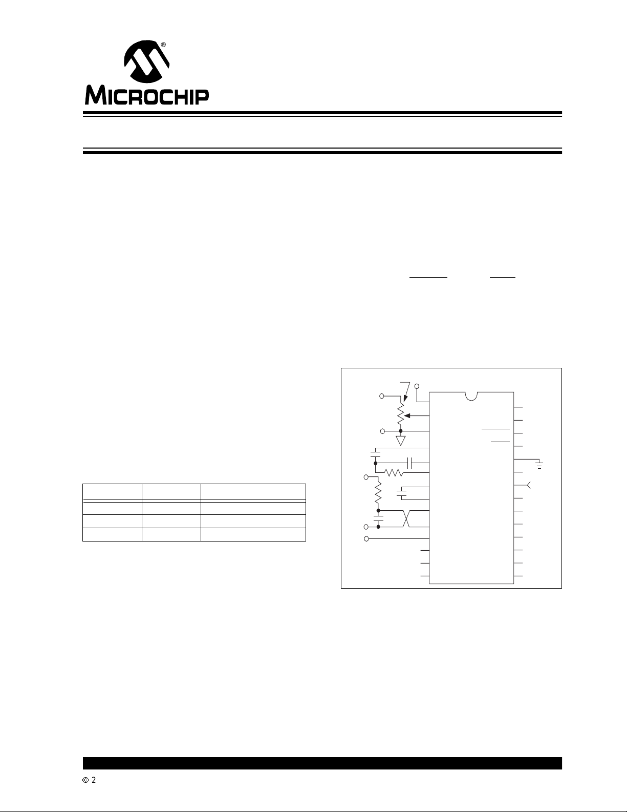
Functional Block Diagram
SET V
REF
IN
V
REF
100kΩ
Analog GND
0.47µF
Signal
Input
+
5V
= 1V
100kΩ
100
kΩ
0.1µF
–5V
1µF
1µF
1
2
3
4
5
6
7
8
9
10
11
12
13
14
TC7135
V-
UNDERRANGE
REF IN
ANALOG
COMMON
INT OUT
AZ IN
BUFF OUT
C
C
-INPUT
+INPUT
V+
D5 (MSD)
B1 (LSB)
B2
REF
REF
+
OVERRANGE
STROBE
RUN/HOLD
DIGTAL GND
POLARITY
CLOCK IN
BUSY
(LSD) D1
D2
D3
D4
(MSB) B8
B4
28
27
26
25
24
23
22
21
20
19
18
17
16
15
Clock
Input
120kH
2002 Microchip TechnologyInc. DS21460B-page 1
TC7135
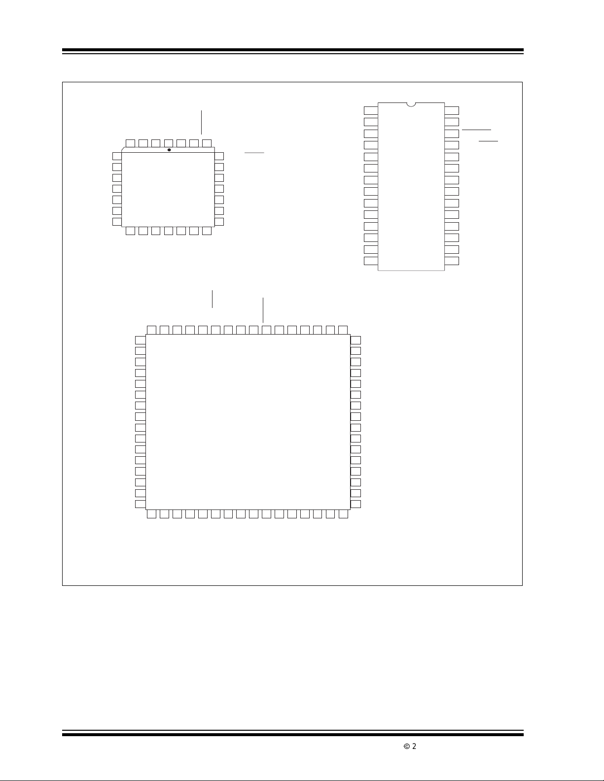
Package Types
AZ IN
BUFF OUT
REF CAP–
REF CAP+
–INPUT
+INPUT
V+
OVERRANGE
UNDERRANGE
ANALOG COM
28-Pin PDIP
INT OUT
ANALOG
COM
4 3 2 1 27 2628
5
6
7
8
9
10
11
12 13 14 15 17 18
REF INV–URORSTROBE
TC7135
B2
(LSB) B1
(MSD) D5
NC
63 61 60 59 58 57 56 55 545352 51 50 4964
1
l
NC
2
NC
3
NC
4
NC
5
NC
6
NC
7
8
9
NC
10
V-
11
REF IN
12
13
NC
14
NC
15
NC
16
NC
17 18 19 20 21 22 23 24 25 26 27 28 29 30 31
NC
16
B4
(MSB) B8
NCNCNC
62
NC
AZ IN
INT OUT
D4
D3
STROBE
NC
25
RUN/HOLD
24
DIGTAL GND
23
POLARITY
22
CLOCK IN
21
BUSY
20
D1 (LSD)
19
D2
64-Pin PQFP
DGND
POLNCCLOCK IN
RUN/HOLD
TC7135
NC
REF
C
BUFF OUT
NC
+
REF
C
BUSYD2D1
NC
–INPUT
NC
REF IN
ANALOG
INT OUT
BUFF OUT
C
– INPUT
+INPUT
(MSD) D5
(LSB) B1
NC
NC
NC
+INPUT
AZ IN
C
32
COM
REF
REF
NC
V+
V+
48
47
46
45
44
43
42
41
40
39
38
37
36
35
34
33
28-Pin PDIP
UNDERRANGE
1
V-
2
3
4
5
6
-
7
+
B2
NC
NC
NC
D3
D4
B8
B4
B2
NC
B1
D5
NC
NC
NC
NC
NC
TC7135
8
9
10
11
12
13
14
28
27
26
25
24
23
22
21
20
19
18
17
16
15
OVERRANGE
STROBE
RUN/HOLD
DIGTAL GND
POLARITY
CLOCK IN
BUSY
D1 (LSD)
D2
D3
D4
B8 (MSB)
B4
NOTE: NC = No internal connection.
DS21460B-page 2
2002 Microchip TechnologyInc.
TC7135
1.0 ELECTRICAL SPECIFICATIONS
Absolute Maximum Ratings*
Positive Supply Voltage..........................................+6V
Negative Supply Voltage.......................................- 9V
Analog Input Voltage (Pin 9 or 10)....V+ to V- (Note 2)
*Stresses above those listed under "Absolute Maximum Ratings"maycause permanentdamage to thedevice.These are
stress ratings only and functional operation of the device at
these or any other conditions above those indicated in the
operation sections of the specifications is not implied. E xposure to Absolute Maximum R ating conditions for extended
periodsmay affectdevice reliability.
Reference Input Voltage (Pin 2)...................... V+ to V-
Clock Input Voltage........................................ 0V to V+
Operating Temperature Range ...............0°C to +70°C
StorageTemperature Range............– 65°C to +150°C
Package Power Dissipation;(T
≤ 70°C)
A
28-Pin PDIP ..................................... 1.14Ω
28-Pin PLCC .................................... 1.00Ω
64-Pin PQFP.....................................1.14Ω
TC7135 ELECTRICAL S PECIFICATIONS
Electrical Characteristics: TA=+25°C,F
(see Functional Block Diagram).
Symbol Parameter Min Typ Max Unit Test Conditions
Analog
Display Reading with Zero VoltInput -0.0000 ±0.0000 +0.0000 D isplay Reading Note 2 and Note 3
Zero Reading Temperature Coefficient — 0.5 2 µV/°C VIN=0V,(Note4)
TC
Z
TC
±FSE ± Full Scale Symmetry Error
Digital
Note 1: Limit input current to under 100µA if input voltages exceedsupply voltage.
Full ScaleTemperature Coefficient — — 5 ppm/°C VIN=2V,
FS
NL Nonlinearity Error — 0.5 1 Count Note 6
DNL Differential LinearityError — 0.01 — LSB Note 6
Display Reading in Ratiometric Operation +0.9996 +0.9999 +1.0000 Display Reading V
(Rollover Error)
Input Leakage Current — 1 10 pA Note 3
I
IN
Noise — 15 — µV
e
N
Input Low Current — 10 100 µAV
I
IL
Input High Current — 0.08 10 µAV
I
IH
OutputLowVol tage — 0.2 0.4 V IOL=1.6mA
V
OL
OutputHighVoltage;
V
OH
B
1,B2,B4,B8,D1–D5
Busy, Polarity,Overrange,
Underrange, Strobe
ClockFrequency 0 200 1200 kHz Note8
F
CLK
2: Full scalevoltage = 2V.
=0V.
3: V
IN
4: 30°C ≤ T
5: .External referencetemperaturecoefficientless than 0.01ppm/°C.
6: -2V ≤ V
7: IV
IN
8: Specification related to clock frequency range over which the TC7135 correctly performs its various functions. Increased
≤ +70°C
A
≤ +2V. Error of readingfrom best fit straightline.
IN
| = 1.9959.
errors result at higher operating frequencies.
= 120kHz, V+ = +5V, V- = -5V,unless otherwise specified
CLOCK
— 0.5 1 Count -V
2.4 4.4 5 V I
4.9 4.99 5 V I
P-P
(Note4andNote5)
=+V
(Note 2)
(Note 7)
IN,
IN=VREF,
IN
Peak-to-Peak Valuenot
Exceeded 95% of Time
=0V
IN
=+5V
IN
=1mA
OH
=10µA
OH
2002 Microchip TechnologyInc. DS21460B-page 3
TC7135
TC7135 ELECTRICAL S PECIFICATIONS (CONTINUED)
Electrical Characteristics: TA=+25°C,F
(see Functional Block Diagram).
Symbol Parameter Min Typ Max Unit Test Conditions
Power Supply
V+ Positive Supply Voltage 4 5 6 V
V- Negative Supply Voltage -3 -5 -8 V
I+ Positive Supply Current — 1 3 mA F
I- Negative Supply Current — 0.7 3 mA F
PD Power Dissipation — 8.5 30 mW F
Note 1: Limit input current to under 100µA if input voltages exceedsupply voltage.
2: Full scalevoltage = 2V.
=0V.
3: V
IN
4: 30°C ≤ T
5: .External referencetemperaturecoefficientless than 0.01ppm/°C.
6: -2V ≤ V
7: IV
IN
8: Specification related to clock frequency range over which the TC7135 correctly performs its various functions. Increased
errors result at higher operating frequencies.
≤ +70°C
A
≤ +2V. Error of readingfrom best fit straightline.
IN
| = 1.9959.
= 120kHz, V+ = +5V, V- = -5V,unless otherwise specified
CLOCK
CLK
CLK
CLK
=0Hz
=0Hz
=0Hz
DS21460B-page 4
2002 Microchip TechnologyInc.
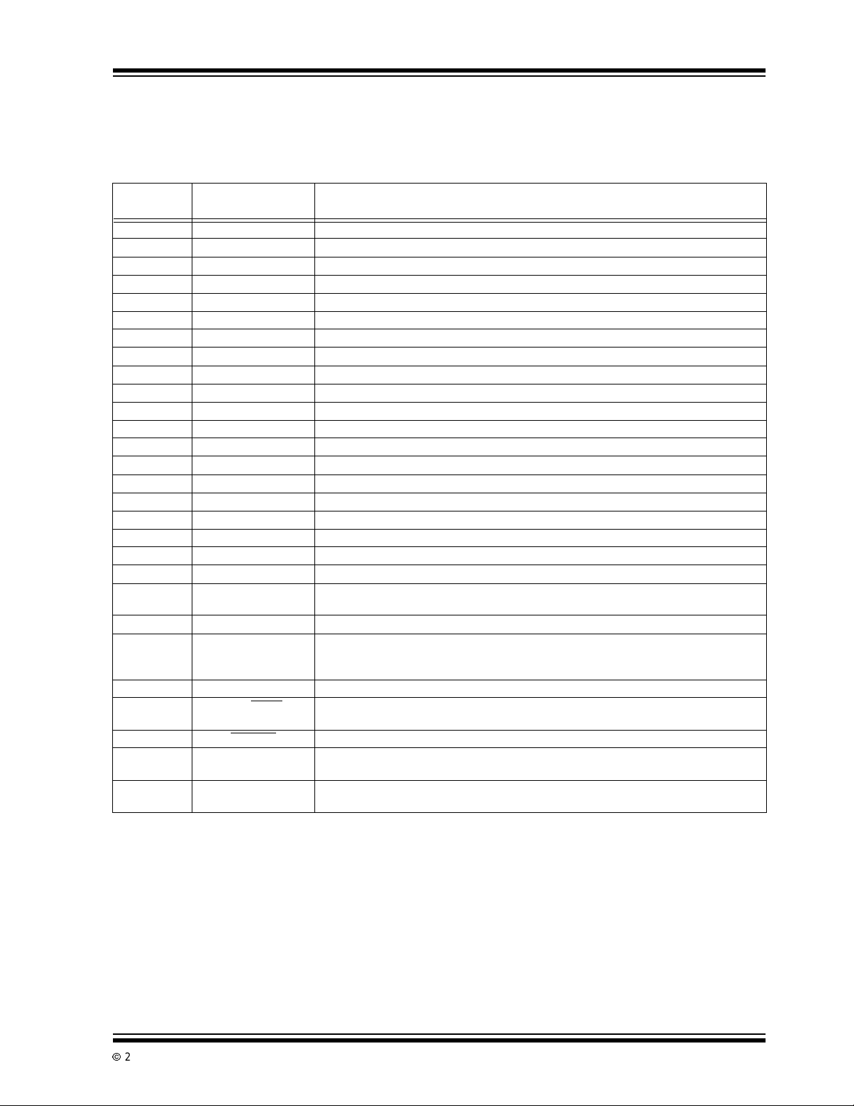
2.0 PIN DESCRIPTIONS
The description of t he pins are listed in Table 2-1.
TABLE 2-1: PIN FUNCTION TABLE
TC7135
Pin Number
28-Pin PDIP
1 V- Negative power supplyinput.
2 REF IN External reference input.
3 ANALOG COMMON Reference point for REF IN.
4 INT OUT Integrator output. Integratorcapacitor connection.
5 AZ IN Auto zero inpt. Auto-zero capacitor connection.
6 BUFF OUT Analog input buffer output. Integrator resistor connection.
7C
8C
9 -INPUT Analoginput. Analog input negativeconnection.
10 +INPUT Analog input. Analog input positive connection.
11 V+ Positive power supplyinput.
12 D5 Digit drive output. Most Significant Digit (MSD)
13 B1 Binary Coded Decimal(BCD) output.LeastSignificantBit (LSB)
14 B2 BCD output.
15 B4 BCD output.
16 B8 BCD output. Most Significant Bit (MSB)
17 D4 Digit drive output.
18 D3 Digit drive output.
19 D2 Digit drive output.
20 D1 Digit drive output. Least Significant Digit (LSD)
21 BUSY Busy output.At the beginningof the signal-integration phase, BUSY goes High and
22 CLOCK IN Clock input. Conversion clock connection.
23 POLARITY Polarity output.A positive input is indicated by a logicHighoutput. The polarity outputis
24 DGND Digitallogicreference input.
25 RUN/HOLD
26 STROBE
27 OVERRANGE Over range output. A logic High indicates that the analog input exceeds the full scale input
28 UNDERRANGE Under range output.A logic High indicates that the analog input is less than 9% of the full
Symbol Description
- Reference capacitor input. Referencecapacitornegative connection.
REF
+ Reference capacitor input. Reference capacitorpositive connection.
REF
remainsHighuntilthefirstclockpulseafter the integratorzerocrossing.
valid at the beginning of the reference integrate phase andremains valid until determined
duringthenext conversion.
Run / Hold input. When at a logic High, conversions are performedcontinuously.A logic
Low holds the current data as long as the Low condition exists.
Strobe output. The STROBE output pulses low in the center of the digit drive outputs.
range.
scaleinputrange.
2002 Microchip TechnologyInc. DS21460B-page 5
TC7135
3.0 DETAILED DESCRIPTION
(All Pin Designations Refer to 28-Pin DIP)
3.1 Dual Slope Conversion P rinciples
The TC7135 is a dual slope, integrating A/ D converter.
An understanding of the dual slope conversion technique will aid i n following the detailed TC7135
operational theory.
The conventional dual slope converter measurement
cycle has two distinct phases:
1. Input signal integration
2. Reference voltage integration ( de-integration)
The input signal being converted is integrated for a
fixed time period. Time is measured by counting clock
pulses.An opposite polarity constant referencevoltage
is then integrated until the integrator output voltage
returns to zero. The reference integration time is
directly proportional to the input signal.
In a simple dual slope converter, a complete conversion requires the integrator output to "ramp-up" and
"ramp-down."
A simple mathematical equation relates the input signal, reference voltage, and integration time:
EQUATION 3-1:
T
1
R
INTCINT
INT
∫
0
VIN(T)DT =
where:
V
T
T
= Reference voltage
REF
= Signal integration time (fixed)
INT
= Reference voltage integration time
DEINT
(variable).
For a constant VIN:
EQUATION 3-2:
V
REFTDEINT
VIN=
The dual slope converter accuracy is unrelated to the
integrating resistor and capacitor values, as long as
they are stable during a measurement cycle. An inher-
T
INT
V
REFTDEINT
R
INTCINT
ent benefit is noise immunity. Noise spikes are integrated, or averaged, to zero during the integration
periods.
Integrating ADCs are immune to the large conversion
errors that plague successive approximation converters in high-noise environments(see Figure 3-1).
FIGURE 3-1: BASIC DUAL SLOPE
CONVERTER
Analog Input
Signal
REF
Voltage
Output
Integrator
Fixed
Signal
Integrate
Time
Integrator
-
+
Switch
Drive
Polarity Control
Display
Variable
Reference
Integrate
Time
Phase
Control
V
IN
V
IN
≈ V
REF
≈ 1/2 V
Comparator
-
+
Control
Logic
REF
Clock
Counter
3.2 TC7135 Operational Theory
The TC7135 incorporates a system zero phase and
integratoroutputvoltage zero phase to the normal twophase dual-slope measurement cycle. Reduced system errors, fewer calibration steps, and a shorter overrange recovery time result.
The TC7135 measurement cycle contains four phases:
1. System zero
2. Analog i nput signal integration
3. Reference voltage integration
4. Integrator output zero
Internal analog gate status for each phase is shown in
Figure 3-1.
TABLE 3-1: INTERNAL ANALOG GATE STATUS
Conversion Cycle Phase SWISWRI+SWRI-SWZSW
System Zero Closed Closed Closed Figure 3-2
InputSignal Integration Closed Figure 3-3
Reference Voltage Integration Closed* Closed Figure 3-4
Integrator OutputZero Closed Closed Figure 3-5
*Note: Assumes a positive polarity input signal. SW
DS21460B-page 6
would be closed for a negative input signal.
RI
SW
R
SW
1
2002 Microchip TechnologyInc.
Reference Figures
IZ
TC7135
A
A
3.2.1 SYSTEM ZERO
During this phase, errors due to buffer, integrator, and
comparator offset voltages are compensated for by
charging C
(auto zero capacitor) with a compensat-
AZ
ing error voltage. With a zero input voltage the integrator output will remain at zero.
The externalinputsignal is disconnectedfromtheinternal circuitry by opening the t wo SW
switches. The
I
internal input points connect to ANALOG COMMON.
The reference capacitor charges to the reference voltage potential through SW
around the integrator and comparator, chargesthe C
. A feedback loop, closed
R
AZ
capacitorwithavoltage to compensate for bufferamplifier, integrator, and comparator offset voltages (see
Figure 3-2).
FIGURE 3-2: SYSTEM ZERO PHASE
Analog
SWRI+
C
REF
Input Buffer
SW
1
+
-
SWIZSW
SW
Z
C
R
INT
INT
C
SZ
Z
-
Comparator
+
+
-
Integrator
Switch Open
Switch Closed
To Digital
Section
+IN
REF
Analog
Common
–
SW
I
SWRI-
SW
R
IN
SW
Z
SWRI+SWRI-
SW
I
IN
3.2.2 ANALOG INPUT SIGNAL
INTEGRATION
The TC7135 integratesthe differentialvoltage between
the +INPUT and -INPUT pins. The differential voltage
must be within the device Common mode range; - 1V
from either supply rail, typically. The input signal polarity is determined at the end of this phase.
SeeFigure2-3
FIGURE 3-3: INPUT SIGNAL
INTEGRATION PHASE
Analog
SW
Input Buffer
+
-
+SWRI-
RI
SW
SW
SW
IZ
SW
Z
1
C
REF
C
R
INT
INT
C
SZ
Z
-
Comparator
+
+
-
Integrator
Switch Open
Switch Closed
To
Digital
Section
nalog
Common
.
+IN
REF
–
SW
I
SW
R
IN
SW
Z
SWRI+SWRI-
SW
I
IN
3.2.3 REFERENCE VOLTAGE
INTEGRATION
The previously-charged reference capacitor is connected with the proper polarity to ramp the integrator
output back to zero
(see Figure 3-4). The digital
reading displayed is:
EQUATION 3-3:
Reading = 10,000
[Differential I nput]
V
REF
FIGURE 3-4: REFERENCE VOLTAGE
INTEGRATION CYCLE
Analog
SWRI+
-
C
REF
+SWRI-
Input Buffer
SW
1
C
R
INT
INT
+
-
SW
IZ
SW
Z
C
SW
SZ
Z
-
Comparator
+
+
-
Integrator
Switch Open
Switch Closed
To Digital
Section
+IN
REF
Analog
Common
–
SW
I
SW
RI
SW
R
IN
SW
Z
SW
RI
SW
I
IN
3.2.4 INTEGRATOR OUTPUT ZERO
This phase ensures the integrator output is at 0V when
the system zero phase is entered. It also ensures that
the true system offset voltages are compensated for.
This phase normally lasts 100 to 200 clockcycles. If an
overrange condition exists, t he phase is extended to
6200 clock cycles (see Figure 3-5).
FIGURE 3-5: INTEGRATOR OUTPUT
ZERO PHASE
Analog
Input Buffer
SWRI+SWRI-
C
REF
SW
1
SW
R
SW
INTCINT
C
SW
IZ
Z
SZ
Z
-
+
Integrator
Switch Open
Switch Closed
Comparator
+
-
To Digital
Section
+
-
+
IN
REF
IN
nalog
Common
–
IN
SW
SW
SW
SW
I
R
Z
SWRI+SWRI-
I
2002 Microchip TechnologyInc. DS21460B-page 7

TC7135
4.0 ANALOG SECTION
FUNCTIONAL DESCRIPTION
4.1 Differential Inputs
The TC7135 operates with differential voltages
(+INPUT, pin 10 and -INPUT, pin 9) within the input
amplifierCommonmode range,which extendsfrom1V
below the positive supply to 1V above the negative
supply. Within this Common mode voltage range, an
86dB Common mode rejection ratio is typical.
The integrator output also follows the Common mode
voltage and must not be allowed to saturate. A worstcase condition exists, for example, when a large positive Common mode voltage with a near full scale negative differential input voltage is applied. The negative
input signal drives the integrator positive when most of
its swing has been used up by the positive Common
mode voltage. For these critical applications, the
integrator swing can be reduced to less than the
recommended 4V full scale swing, with some loss of
accuracy. The integrator output can swing within 0.3V
of either supply without loss of linearity.
4.2 Analog Comm on Input
ANALOG COMMON is used as the -INPUT return during auto zero and de-integrate. If -INPUT is different
from ANALOG COMMON, a Common mode voltage
existsin the system. However, this signal is rejected by
the excellent CMRR of the converter. In most applications, –INPUT will be set at a fixed, known voltage
(power supply common, for instance). In this application, ANALOG COMM ON should be tied to the same
point, thus removing the Common mode voltage from
the converter. The reference voltage is referenced to
ANALOG COMMON.
FIGURE 4-1: USING AN EXTERNAL
REFERENCE
V+
TC7135
REF
IN
ANALOG
COMMON
10k
10k
MCP1525
2.5 V
REF
1µF
Analog Ground
V+
4.3 Reference Voltage Input
The reference voltage input (REF IN) must be a positivevoltagewithrespecttoANALOGCOMMON.A
reference voltage circuit is shown in Figure 4-1.
DS21460B-page 8
2002 Microchip TechnologyInc.

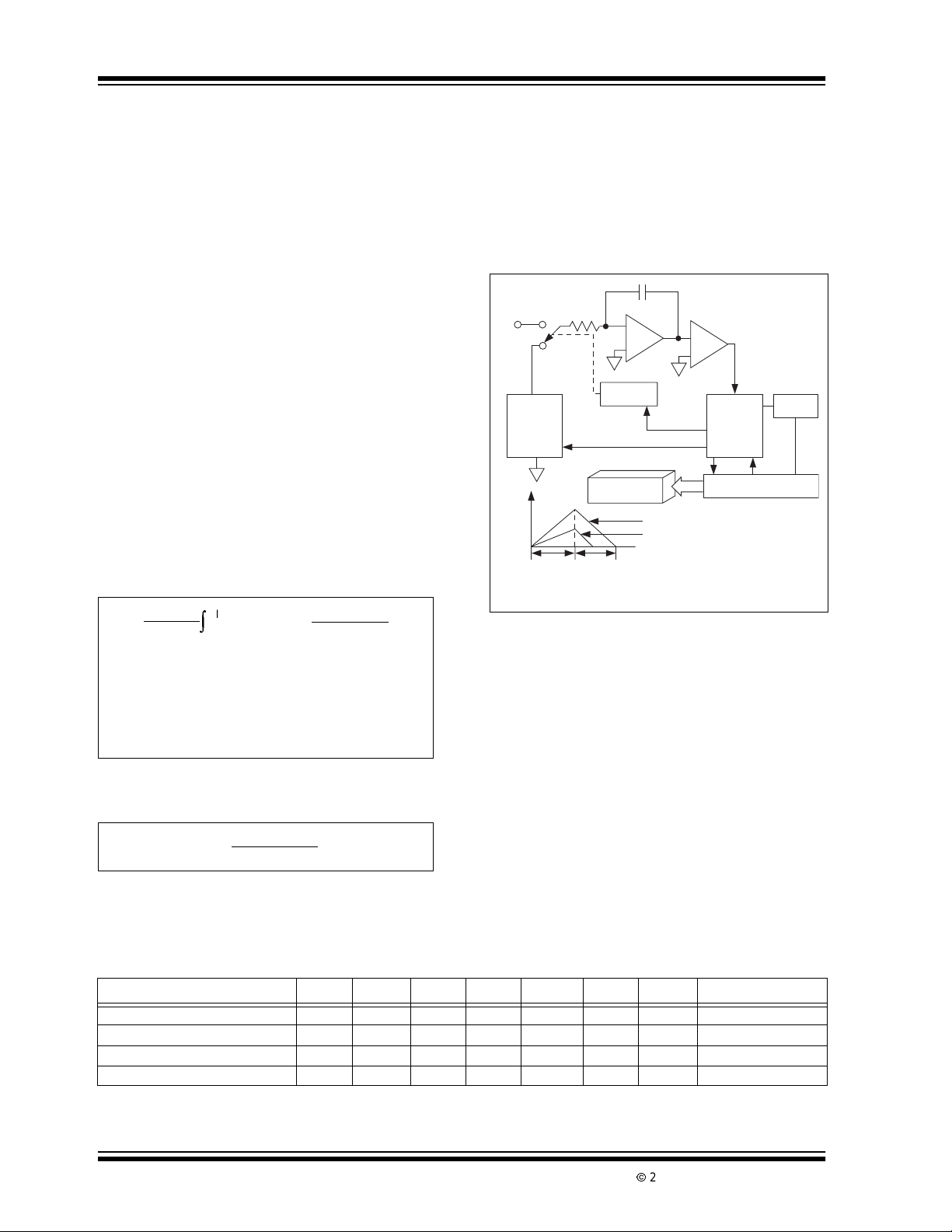
5.0 DIGITAL SECTION
FUNCTIONAL DESCRIPTION
The major digital subsystems within the TC7135 are
illustrated in Figure 5-1, with timing relationships
shown in Figure 5-2. The multiplexed BCD output data
can be displayed on LCD or LED displays. The digital
section is best described through a di scussion of the
control signals and data outputs.
FIGURE 5-1: DIGITAL SECTION FUNCTIONAL DIAGRAM
TC7135
Polarity
From
Analog
Section
Polarity
FF
Zero
Cross
Detect
24 22 25 27 28 26 21
DGND Clock
In
D5 D4 D3 D2 D1
MSB Digit Drive Signal LSB
Multiplexer
Latch Latch Latch Latch Latch
Counters
Control Logic
RUN/
HOLD
Overrange STROBE BusyUnderrange
Data
Output
13 B1
14 B2
15 B4
16 B8
2002 Microchip TechnologyInc. DS21460B-page 9

TC7135
FIGURE 5-2: TIMING DIAGRAMS FOR
OUTPUTS
Integrator
Output
Busy
Overrange when
Applicable
Underrange when
Applicable
Digit Scan
STROBE
Digit Scan
for Overrange
Signal
Integrate
System
10,000
Zero
Counts
10,001
(Fixed)
Counts
Full Measurement Cycle
40,002 Counts
Expanded Scale Below
100
Counts
Auto Zero
*
D5
D4
D3
D2
D1
Reference
Integrate
20,001
Counts (Max)
D5
D4
D3
D2
D1
First D5 of System Zero and
*
Reference Integrate One Count
Longer
*
Reference
Integrate
Signal
Integrate
5.1 RUN/HOLD Input
When left open, this pin assumes a logic "1" level. With
a RUN/HOLD
continuously, with a new measurement cycle beginning
every 40,002 clock pulses.
When RUN/HOLD
ment cyclein progresswillbecompleted,dataheldand
displayed, as long as the logic "0" condition exists.
A positive pulse (>300nsec) at RUN/HOLD
new measurement cycle. The measurement cycle in
progress when RUN/HOLD
"0" state must be completed before the positive pulse
can be recognized as a single conversion run
command.
The new measurement cycle begins with a 10,001count auto zero phase. At the end of this phase the
busy signal goes high.
= 1, the TC7135 performs conversions
changestoa logic "0," the measure-
initiates a
initially assumed the logic
5.2 STROBE Output
During the measurement cycle, the STROBE control
line is pulsed l ow five times. The five low pulses occur
in the center of the digit drive signals (D
(see Figure 5-3).
D
(MSD) goes high for 201 counts when the measure-
5
ment cycles end. I n the center of the D
clock pulses after the end of the measurement cycle,
the first STROBE
the D
digit s trobe, D4goes high for 200 clock pulses.
5
The STROBE
occurs for one half clock pulse. After
then goes low 100 clock pulses after D
goes high. This continues through the D1digit drive
pulse.
The digit drive signals will continue to permit display
scanning.STROBE
pulsesarenotrepeateduntilanew
measurement is completed. The digit drive signals will
not continue if the previous signal resulted in an
overrange condition.
TheactivelowSTROBE
pulses aid BCD data transfer
to UARTs, pr ocessors and external latches. For more
information,please refer to Application Note 784.
FIGURE 5-3: STROBE SIGNAL LOW
FIVE TIMES PER
CONVERSION
TC835
Outputs
Busy
B1–B8
STROBE
D5
D4
D3
D2
D1
*Delay between Busy going Low and First STROBE pulse is
dependent on Analog Input.
End of Conversion
*
D5 (MSD)
Data
200
Counts
201
Counts
D4
Data
200
Counts
D3
DataD2Data
200
Counts
200
Counts
1,D2,D3,D5
pulse, 101
5
D1 (LSD)
DataD5Data
Note Absence of
STROBE
Counts
200
Counts
200
)
4
DS21460B-page 10
2002 Microchip TechnologyInc.

5.3 BUSY O utput
At the beginning of the signal integration phase, BUSY
goes high and remains high until the first clock pulse
after the i ntegrator zero crossing. BUSY returns to the
logic "0" state after the measurement cycle ends in an
overrange condition. The internal display latches are
loaded during the first clock pulse after BUSY and are
latched at the clock pulse end. The BUSY signal does
not go high at the beginningof the measurementcycle,
which starts with the auto zero cycle.
5.4 OVERRANGE Output
If the input signal causes the reference voltage integration time to exceed 20,000 clock pulses, the OVERRANGE output i s set to a logic "1." The overrange
output register is set when BUSY goes low and is reset
at the beginning of the next reference integration
phase.
5.5 UNDERRANGE Output
If the output count is 9% of full scale or less (-1800
counts), the underrange register bit is set at the end of
BUSY. The bit is s et low at the next signal integration
phase.
TC7135
5.6 POLARITY Output
A positive input is registered by a logic "1" polarity signal. The polarity bit is valid at the beginning of reference integrate and remains valid until determined
during the next conversion.
The polarity bit is valid even for a zero reading. Signals
lessthan the converter'sLSB will have the signal polarity determined correctly. This is useful in null
applications.
5.7 Digit Drive Outputs
Digit drive signals are positive-going signals. The scan
sequence is D
pulses wide, with the exception D
pulses wide.
All five digits are scanned continuously, unless an
overrange condition occurs. In an overrange condition,
all digit drives are held low from the final STROBE
pulseuntil the beginning of the next referenceintegrate
phase. The scanning sequence is then repeated. This
provides a blinking visual display indication.
to D1. All positive pulses are 200 clock
5
, which is 201 clock
5
5.8 BCD Da ta Outputs
The binarycodeddecimal(BCD)bitsB8,B4,B2,and B
are positive-true logic signals. The data bits become
active at the same time as the digit drive signals. In an
overrangecondition, all data bitsareata logic "0" state.
1
2002 Microchip TechnologyInc. DS21460B-page 11

TC7135
6.0 TYPICAL APPLICATIONS
6.1 Component Value Selection
6.1.1 INTEGRATING RESISTOR
The i ntegrating resistor R
scale input voltage and the output current of the buffer
used to charge the integrator capacitor, C
bufferamplifier and the integrator havea class A output
stage, with 100µA of quiescent current. A 20µAdrive
current gives negligible linearity errors. Values of 5µA
to 40µA gi ve good results. The exact value of an
integrating resistor for a 20µA current is easily
calculated.
EQUATION 6-1:
R
Full scale voltage
=
INT
6.1.2 INTEGRATING CAPACITOR (
The productof integratingresistor and capacitorshould
be selected to give the maximum voltage swing that
ensures the tolerance buildup will not saturate the integrator swing (approximately 0.3V from either supply).
For ±5V supplies and ANALOG COMMON tied to supply ground, a ±3.5V to ±4V full scale integratorswing is
adequate. A 0.10µFto0.47µF is recommended. In
general, the value of C
EQUATION 6-2:
C
INT
[10,000 x clock period] x I
=
Integrator output voltage swing
(10,000) (clock period) (20µA)
=
Integrator output voltage swing
is determined by the full
INT
20µA
is given by:
INT
. Both the
INT
C
INT
INT
)
The dielectricabsorption of the referenceandautozero
capacitors are only important at power-on or when the
circuit is recovering from an overload. Smaller or
cheaper capacitors can be used if accurate readings
are not required for t he first few seconds of recovery.
6.1.4 REFERENCE VOLTAGE
The analog input required to generate a full scale output is V
IN
=2V
REF
.
The stabilityofthe referencevoltage is a major factor in
the overall absolute accuracy of the converter. For this
reason,it is recommendedthata high-qualityreference
be used where high-accuracy absolute measurements
are being made.
6.2 Conversion Timing
6.2.1 LINE FREQUENCY REJECTION
A signal integrationperiod at a multipleof the 60Hz line
frequency will maximize 60Hz "line noise" rejection. A
100kHz clock f requency will reject 50Hz, 60Hz and
400Hz noise. This corresponds to five readings per
second (see Table 6-1 and Table 6-2).
TABLE 6-1: CONVERSION RATE VS.
CLOCK FREQUEN CY
Oscillator Frequency
(kHz)
100 2.5
120 3
200 5
300 7.5
400 10
800 20
1200 30
Conversion Rate
(Conv./Sec.)
A very importantcharacteristicof the integratingcapacitor C
is that it has low dielectric absorption t o pre-
INT
vent rollover or ratiometric errors. A good test for
dielectric absorption is to use the capacitor with the
input tied to the reference. This ratiometric condition
should read half scale 0.9999, with any deviation
probably due to dielectric absorption. Polypropylene
capacitorsgiveundetectable errors at reasonablecost.
Polystyreneand polycarbonatecapacitorsmay also be
used in less critical applications.
6.1.3 AUTO ZERO AND REF ERENCE
CAPACITORS
The size of the auto zero capacitor has some influence
on the noise of the system. A large capacitor reduces
the noise. The reference capacitor should be large
enough such that stray capacitance t o ground from its
nodes is negligible.
DS21460B-page 12
2002 Microchip TechnologyInc.

TC7135
TABLE 6-2: LINE FREQUENCY
REJECTION VS. CLOCK
FREQUENCY
Oscillator Frequency
(kHz)
300 60
200
150
120
100
40
33-1/3
250 50
166-2/3
125
100
100 50,60,400
The c onversion rate is easily calculated:
Line Frequency Rejection
(Hz)
EQUATION 6-3:
Reading 1/sec =
Clock Frequency (Hz)
4000
6.3 High Speed Operation
The maximum conversion rate of most dual slope A/D
converters is limited by the f requency response of the
comparator. The comparator in this circuit follows the
integrator ramp with a 3µsecdelay,ataclockfrequency of 160 kHz (6µsec period), Half of the first reference integrate clock period is lost in delay. This
means that the meter reading will change from 0 t o 1
witha50µV input, 1 to 2 with 150µV,2to3at250µV,
etc. This transition at midpoint is considered desirable
by most users. However, if the clock frequency is
increased appreciably above 200kHz, the instrument
will flash "1" on noise peaks, even when the input is
shorted.
For many dedicated applications where the input signal
is always of one polarity, the delay of the comparator
need not be a limitation. Since the nonlinearity and
noisedonotincreasesubstantiallywith frequency, clock
ratesofupto~1MHzmaybeused.Forafixedclockfrequency, the extracount,orcounts, causedby comparator delay, will be a constant and can be subtracted out
digitally.
The clock frequency may be extended above 160kHz
without this error, however, by using a low value resistor in series with the integrating capacitor. The effect of
the resistor is to introduce a small pedestal voltage on
to the integrator output at the beginning of the reference integrate phase. By careful selection of the ratio
between this resistor and the integrating resistor (a few
tens of ohms in the recommended circuit),the compar-
ator delay can be compensated and the maximum
clock frequency extended by approximately a factor of
3. At higher frequencies, ringing and second-order
breaks will cause significant nonlinearities in the first
few counts of the instrument.
The minimum clock frequency is established by leakage on the auto zero and reference capacitors. W ith
most devices, measurement cycles as long as 10 seconds give no measurable leakage error.
The clock used should be free from significant phaseor
frequency jitter. Several suitable low-cost oscillators
are shown in Section 6.0, Typical Applications. The
multiplexed output means that if the display takes significant current from the logic supply, the clock should
have good PSRR.
6.4 Zero Crossing Flip Flop
The flip flop interrogates the data once every clock
pulseafterthetransientsofthe previousclockpulseand
half clock pulse have died down. False zero crossings
caused by clock pulses are not recognized. Of course,
the flip flop delays the true zero crossing by up to one
count in every instance. If a correction were not made,
the display would always be one count too high. Therefore, the counter is disabled for one clock pulse at the
beginning of the reference integrate (de-integrate)
phase.Thisone-count delaycompensates for the delay
of the zero crossing flip flop and allows the correct number to be latched into the display. Similarly, a one-count
delay at the beginning of auto zero gives an overload
displayof0000instead of 0001.Nodelayoccursduring
signal integrate so that true ratiometric readings result.
6.5 Generating a Negative Supply
A negative voltage can be generated from the positive
supply by using a TC7660 (see Figure 6-1).
FIGURE 6-1: NEGATIVE SUPPLY
VOLTAGE GENERATOR
+5V
11
TC7135
24
V+
V –
1
(-5V)
10µF
+
5
8
TC7660
4
10µF
+
23
2002 Microchip TechnologyInc. DS21460B-page 13

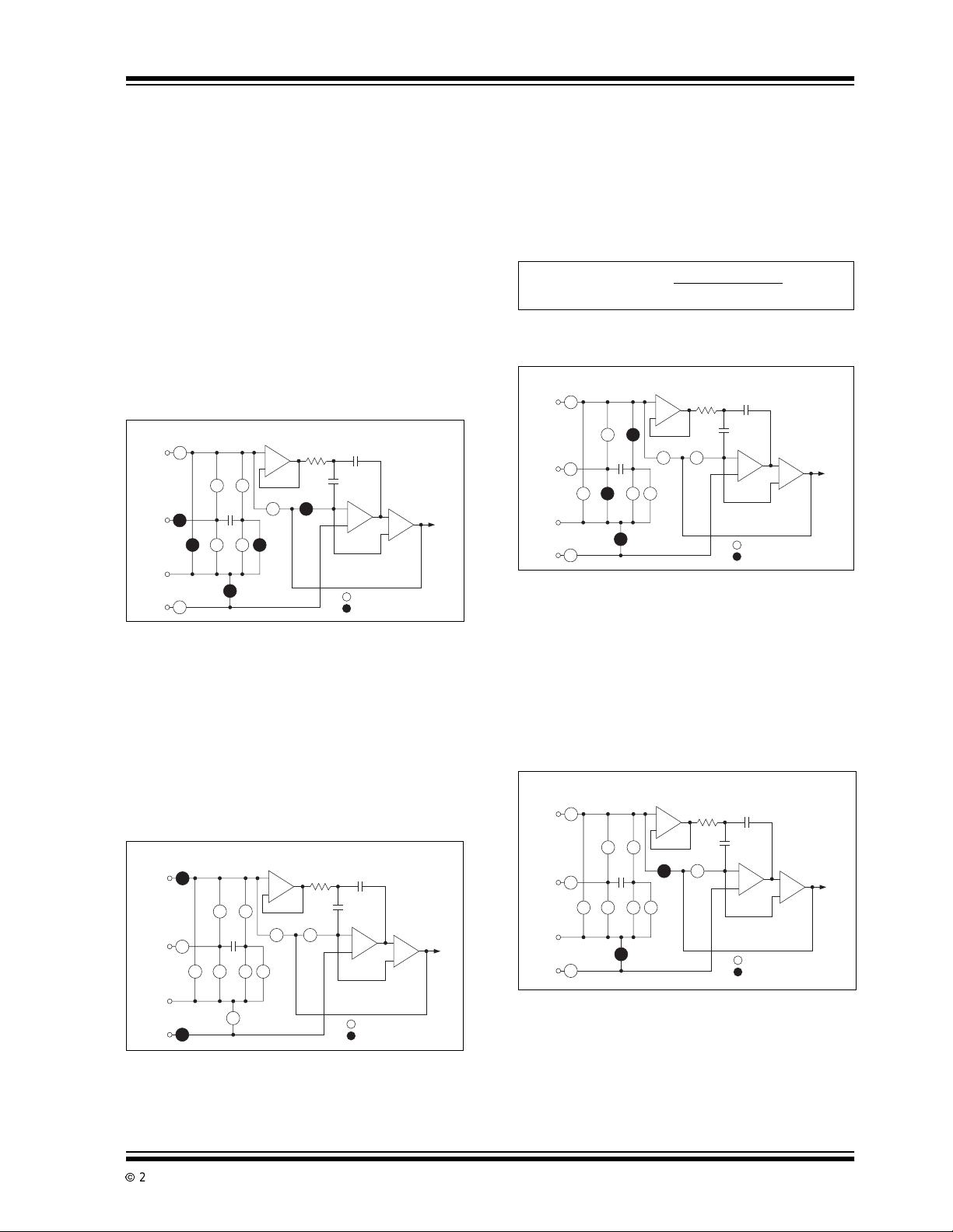
TC7135
A
FIGURE 6-2: 4-1/2 DIGIT ADC WITH MULTIPLEXED COMMON ANODE LED DISPLAY
20 19 18 17 12
D1 D2 D3 D4 D5
4
1µF
1µF
5
6
22
10
9
3
–5V
INT OUT
AZ IN
BUFF
OUT
TC7135
F
IN
+INPUT
–INPUT
ANALOG
COMMON
REF
V–
IN
21
100kΩ
POL
C
REF
C
REF
MCP1525
1µF
B8
B4
B2
B1
V+
4.7kΩ
23
7
-
1µF
8
+
16
15
14
13
11
V+
Blank MSD On Zero
bc
6
D
2
C
1
B
7
A
7777
X7
9–15
5
RBI
DM7447A
16
+
nalog
Input
–
0.33µF
100kΩ
200kHz
100kΩ
+5V
+5V
FIGURE 6-3: RC OSCILLATOR CIRCUIT FIGURE 6-4: COMPARATOR CLOCK
16kΩ
16kΩ
CIRCUITS
2
+
LM311
3
-
4
+5V
2
+
6
LM311
3
4
1
56kΩ
8
R4
2kΩ
7
7
1
C2
10pF
+5V
1kΩ
30kΩ
390pF
R3
50kΩ
V
V
OUT
OUT
R
2
R
1
C
F
O
Gates are 74C04
0.22µF
1. FO=
2C(0.41 R
1
+0.7R1)
P
,R
R1R
=
P
2
R1+R
2
a. If R1=R2=R1,F≅ 0.55/RC
b. If R
>> R1,F≅ 0.45/R1C
2
c. If R
<< R1,F≅ 0.72/R1C
2
2. Examples:
R2
100kΩ
a. F = 120kHz, C = 420pF
R
b. F = 120kHz, C = 420pF, R
R
c. F = 120 kHz, C = 220 pF, R
R
1
1=R2
= 8.93kΩ
1
= 27.3k Ω
≈ 10.9 kΩ
= 50kΩ
2
=5kΩ
2
R2
100kΩ
C1
0.1µF
DS21460B-page 14
2002 Microchip TechnologyInc.

TC7135
V
FIGURE 6-5: 4-1/2 DIGIT ADC W ITH MULTIPLEXED COMMON CATHODE LED DISPLAY
+5V
MCP1525
SIG
IN
1µF
100
+
–
Analog
0.33µF
kΩ
100
GND
0.1
µF
kΩ
1µF
100 kΩ
1µF
+5V
SET V
–5V
1
2
3
4
5
6
7
8
9
10
11
12
13
14
= 1V
REF
V-
TC7135
REF IN
ANALOG
GND
INT
OUT
AZ IN
BUFF
OUT
C
+
REF
-
C
REF
–INPUT
+INPUT
V+
D5 (MSD)
B1 (LSB)
B2
UR
OR
STROBE
RUN/HOLD
DGND
POLARITY
CLK IN
BUSY
(LSD) D1
D2
D3
D4
(MSB) B8
B4
+5V
28
27
150Ω
26
47
kΩ
25
24
23
22
21
20
19
18
17
16
15
F
= 200kHz
OSC
150Ω
10
11
12
13
14
15
16
17
18
MC14513
9
8
7
6
5
4
3
2
1
+5
2002 Microchip TechnologyInc. DS21460B-page 15

TC7135
7.0 PACKAGING INFORMATION
7.1 Package Marking Information
Package marking data not available at this time.
7.2 Taping Forms
Component Taping Orientation for 28-Pin PLCC Devices
PIN 1
User Direction of Feed
W
P
Standard Reel Component Orientation
for TR Suffix Device
Carrier Tape, Number of Components Per Reel and Reel Size
Package Carrier Width (W) Pitch (P) Part Per Full Reel Reel Size
28-Pin PLCC 24 mm 16 mm 750 13 in
Component Taping Orientation for 64-Pin PQFP Devices
DS21460B-page 16
User Direction of Feed
PIN 1
W
P
Standard Reel Component Orientation
for TR Suffix Device
Carrier Tape, Number of Components Per Reel and Reel Size
Package Carrier Width (W) Pitch (P) Part Per Full Reel Reel Size
64-Pin PQFP 32 mm 24 mm 250 13 in
NOTE: Drawing does not represent total number of pins.
2002 Microchip TechnologyInc.

7.3 Package Dimensions
TC7135
28-Pin PDIP (Wide)
.200 (5.08)
.140 (3.56)
.150 (3.81)
.115 (2.92)
.110 (2.79)
.090 (2.29)
1.465 (37.21)
1.435 (36.45)
.070 (1.78)
.045 (1.14)
.022 (0.56)
.015 (0.38)
PIN 1
.555 (14.10)
.530 (13.46)
.040 (1.02)
.020 (0.51)
.015 (0.38)
.008 (0.20)
.610 (15.49)
.590 (14.99)
.700 (17.78)
.610 (15.50)
Dimensions: inches (mm)
˚
MIN.
3
28-Pin PLCC
.495 (12.58)
.485 (12.32)
.456 (11.58)
.450 (11.43)
.456 (11.58)
.450 (11.43)
.495 (12.58)
.485 (12.32)
PIN 1
.050 (1.27) TYP.
.180 (4.57)
.165 (4.19)
Dimensions: inches (mm)
.021 (0.53)
.013 (0.33)
.430 (10.92)
.032 (0.81)
.390 (9.91)
.026 (0.66)
.020 (0.51) MIN.
.120 (3.05)
.090 (2.29)
2002 Microchip TechnologyInc. DS21460B-page 17

TC7135
)
7.3 Packaging Dimensions (Continued)
64-Pin PQFP
˚
MAX.
7
.018 (0.45)
.012 (0.30)
.031 (0.80) TYP.
PIN 1
.555 (14.10)
.547 (13.90)
.687 (17.45)
.667 (16.95)
.555 (14.10)
.547 (13.90)
.687 (17.45)
.667 (16.95)
.009 (0.23)
.005 (0.13)
.130 (3.30) MAX.
Dimensions: inches (mm
.041 (1.03)
.031 (0.78)
.010 (0.25) TYP.
.120 (3.05)
.100 (2.55)
DS21460B-page 18
2002 Microchip TechnologyInc.

TC7135
SALES AND SUPPORT
Data Sheets
Products supportedby a preliminary DataSheetmayhave an erratasheetdescribing minor operationaldifferences and recommendedworkarounds.To determine if an errata sheetexists for a particular device,please contact one of the following:
1. Your local Microchip sales office
2. The Microchip Corporate Literature Center U.S. FAX:(480)7 92-7277
3. The Microchip Worldwide Site (www.microchip.com)
Pleasespecify which device, revision of silicon and Data Sheet (includeLiterature #) you are using.
New Customer Notification System
Register on our web site (www.microchip.com/cn)to receive the most currentinformationon our products.
2002 Microchip Technology Inc. DS21460B-page19

TC7135
NOTES:
DS21460B-page 20 2002 Microchip Technology Inc.

TC7135
Information contained in this publication regarding device
applications and the like is intended through suggestion only
and may be superseded by updates. It is your responsibility to
ensure that your application meets with your specifications.
No representation or warranty is given and no liability is
assumed by Microchip Technology Incorporated with respect
to the accuracy or use of such information, or infringement of
patents or other intellectual property rights arising from such
use or otherwise. Use of Microchip’s products as critical components in life support systems is not authorized except with
express written approval by Microchip. No licenses are conveyed, implicitly or otherwise, under any intellectual property
rights.
Trademarks
The Microchip name and logo, the Microchip logo, FilterLab,
K
EELOQ,microID,MPLAB,PIC,PICmicro,PICMASTER,
PICSTART, PRO MATE, SEEVAL and The Embedded Control
SolutionsCompany areregiste red trademarksof MicrochipTechnologyIncorp or ated in the U.S.A. and other countries .
dsPIC, ECONOMONI TOR, FanSense, FlexROM, fuzzyLAB,
In-Circuit Serial Programming, ICSP, ICEPIC, microPort,
Migratable Memory, MPASM, MPLIB, MPLINK, MPSIM,
MXDEV, PICC, PICDEM, PICDEM.net, rfPIC, Select Mo de
and Total Enduranceare trademarksof MicrochipTechnology
Incorporated in the U.S.A.
Serialized Quick Turn Programming (SQTP) is a service mark
of Microchip Technology Incorporated in the U.S.A.
All other trademarks mentioned herein are property of their
respective companies.
© 2002, Microchip Technology Incorporated, Printed in the
U.S.A., All Rights Reserved.
Printed on recycled paper.
Microchip received QS-9000 quality system
certification for its worldwide headquarters,
design and wafer fabrication facilities in
Chandler and Tempe, Arizona in July 1999
and Mountain View, California in March 2002.
The Company’s quality system processes and
procedures are QS-9000 compliant for its
®
PICmicro
devices, Serial EEPROMs, microperipherals,
non-volatile memory and analog products. In
addition, Microchip’s quality system for the
design and manufacture of development
systemsisISO 9001certified.
2002 Microchip TechnologyInc. DS21460B-page 21
8-bit MCUs, KEELOQ®code hopping

WORLDWIDE SALES AND SERVICE
AMERICAS
Corporate Office
2355 West Chandler Blvd.
Chandler, AZ 85224-6199
Tel: 480-792-7200 Fax: 480-792-7277
Technical Support: 480-792-7627
Web Address: http://www.microchip.com
Rocky Mountain
2355 West Chandler Blvd.
Chandler, AZ 85224-6199
Tel: 480-792-7966 Fax: 480-792-7456
Atlanta
500 Sugar Mill Road, Suite 200B
Atlanta, GA 30350
Tel: 770-640-0034 Fax: 770-640-0307
Boston
2 Lan Drive, Suite 120
Westford, MA 01886
Tel: 978-692-3848 Fax: 978-692-3821
Chicago
333 Pierce Road, Suite 180
Itasca, IL 60143
Tel: 630-285-0071 Fax: 630-285-0075
Dallas
4570 Westgrove Drive, Suite 160
Addison, TX 75001
Tel: 972-818-7423 Fax: 972-818-2924
Detroit
Tri-Atria Office Building
32255 Northwestern Highway, Suite 190
Farmington Hills, MI 48334
Tel: 248-538-2250 Fax: 248-538-2260
Kokomo
2767 S. Albright Road
Kokomo, Indiana 46902
Tel: 765-864-8360 Fax: 765-864-8387
Los Angeles
18201 Von Karman, Suite 1090
Irvine, CA 92612
Tel: 949-263-1888 Fax: 949-263-1338
New York
150 Motor Parkway, Suite 202
Hauppauge, NY 11788
Tel: 631-273-5305 Fax: 631-273-5335
San Jose
Microchip Technology Inc.
2107 North First Street, Suite 590
San Jose, CA 95131
Tel: 408-436-7950 Fax: 408-436-7955
Toronto
6285 Northam Drive, Suite 108
Mississauga, Ontario L4V 1X5, Canada
Tel: 905-673-0699 Fax: 905-673-6509
ASIA/PACIFIC
Australia
Microchip Technology Australia Pty Ltd
Suite 22, 41 Rawson Street
Epping 2121, NSW
Australia
Tel: 61-2-9868-6733 Fax: 61-2-9868-6755
China - Beijing
Microchip Technology Consulting (Shanghai)
Co., Ltd., Beijing Liaison Office
Unit 915
Bei Hai Wan Tai Bldg.
No. 6 Chaoyangmen Beidajie
Beijing, 100027, No. China
Tel: 86-10-85282100 Fax: 86-10-85282104
China - Chengdu
Microchip Technology Consulting (Shanghai)
Co., Ltd., Chengdu Liaison Office
Rm. 2401, 24th Floor,
Ming Xing Financial Tower
No. 88 TIDU Street
Chengdu 610016, China
Tel: 86-28-86766200 Fax: 86-28-86766599
China - Fuzhou
Microchip Technology Consulting (Shanghai)
Co., Ltd., Fuzhou Liaison Office
Unit 28F, World Trade Plaza
No. 71 Wusi Road
Fuzhou 350001, China
Tel: 86-591-7503506 Fax: 86-591-7503521
China - Shanghai
Microchip Technology Consulting (Shanghai)
Co., Ltd.
Room 701, Bldg. B
Far East International Plaza
No. 317 Xian Xia Road
Shanghai, 200051
Tel: 86-21-6275-5700 Fax: 86-21-6275-5060
China - Shenzhen
Microchip Technology Consulting (Shanghai)
Co., Ltd., Shenzhen Liaison Office
Rm. 1315, 13/F , Shenzhen Kerry Centre,
Renminnan Lu
Shenzhen 518001, China
Tel: 86-755-2350361 Fax: 86-755-2366086
China - Hong Kong SAR
Microchip Technology Hongkong Ltd.
Unit 901-6, Tower2, Metroplaza
223 Hing Fong Road
Kwai Fong, N.T., Hong Kong
Tel: 852-2401-1200 Fax: 852-2401-3431
India
Microchip Technology Inc.
India Liaison Office
Divyasree Chambers
1 Floor, Wing A (A3/A4)
No. 11, O’Shaugnessey Road
Bangalore, 560 025, India
Tel: 91-80-2290061 Fax: 91-80-2290062
Japan
Microchip Technology Japan K.K.
Benex S-1 6F
3-18-20, Shinyokohama
Kohoku-Ku, Yokohama-shi
Kanagawa, 222-0033, Japan
Tel: 81-45-471- 6166 Fax: 81-45-471-6122
Korea
Microchip Technology Korea
168-1, Youngbo Bldg. 3 Floor
Samsung-Dong, Kangnam-Ku
Seoul, Korea 135-882
Tel: 82-2-554-7200 Fax: 82-2-558-5934
Singapore
Microchip Technology Singapore Pte Ltd.
200 Middle Road
#07-02 Prime Centre
Singapore, 188980
Tel: 65-6334-8870 Fax: 65-6334-8850
Taiwan
Microchip Technology Taiwan
11F-3, No. 207
Tung HuaNorth Road
Taipei, 105, Taiwan
Tel: 886-2-2717-7175 Fax: 886-2-2545-0139
EUROPE
Denmark
Microchip Technology Nordic ApS
Regus Business Centre
Lautrup hoj 1-3
Ballerup DK-2750 Denmark
Tel: 45 4420 9895 Fax: 45 4420 9910
France
Microchip Technology SARL
Parc d’Activite du Moulin de Massy
43 Rue du Saule Trapu
Batiment A - ler Etage
91300 Massy, France
Tel: 33-1-69-53-63-20 Fax: 33-1-69-30-90-79
Germany
Microchip Technology GmbH
Gustav-Heinemann Ring 125
D-81739 Munich, Germany
Tel: 49-89-627-144 0 Fax: 49-89-627-144-44
Italy
Microchip Technology SRL
Centro Direzionale Colleoni
Palazzo Taurus 1 V. Le Colleoni 1
20041 Agrate Brianza
Milan, Italy
Tel: 39-039-65791-1 Fax: 39-039-6899883
United Kingdom
Microchip Ltd.
505 Eskdale Road
Winnersh Triangle
Wokingham
Berkshire, England RG415TU
Tel: 44 118 921 5869 Fax: 44-118 921-5820
04/20/02
DS21460B-page 22
*DS21460B*
2002 Microchip Technology Inc.
 Loading...