

Page 1
M
150mA, 10V LDO with Shutdown
TC56
Features
• Low Dropout Voltage: 200mV typ. at 80mA,
380mV typ. at 160mA
• High Output Current: 180mA (V
• High Accuracy Output Voltage (±2%)
• Low Power Consumption: 11µA (Oper.),
0.1µA (Shutdown)
• Low Temperature Drift (±100ppm/°C typ.)
• Excellent Line Regulation (0.2%/V typ.)
• Space Saving 5-Pin SOT-23A Package
• Short Circuit Protection
• Standard 2.5V, 3.0V and 3.3V Output Voltages
OUT
= 5.0V)
Applications
• Battery Powered Devices
• Cameras and Portable Video Equipment
• Pagers and Cellular Phones
• Solar Powered Instruments
• Consumer Products
Device Selection Table
Output
Part Number
TC562502ECT 2.5 5-Pin SOT-23A -40°C to +85°C
TC563002ECT 3.0 5-Pin SOT-23A -40°C to +85°C
TC563302ECT 3.3 5-Pin SOT-23A -40°C to +85°C
*Other output voltages are available. Please contact
Microchip Technology Inc. for details.
Voltage
(V)*
Package
Temperature
Range
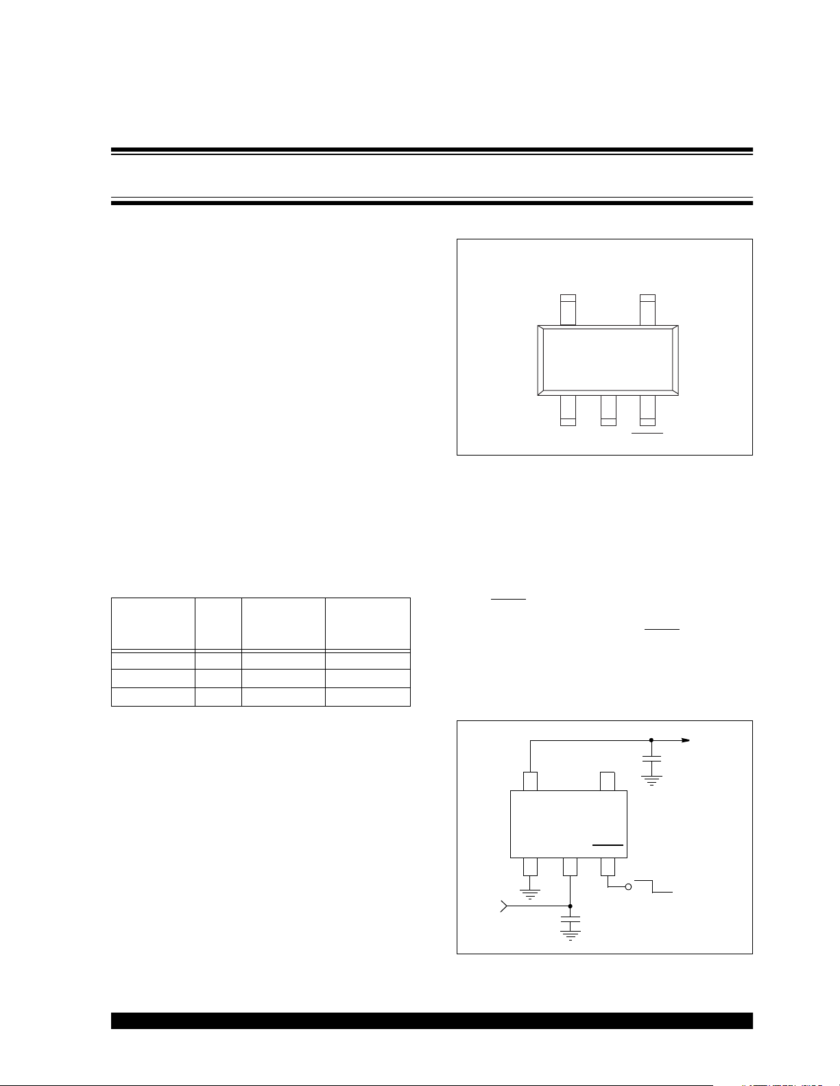
Package Type
5-Pin SOT-23A
V
OUT
5
NC
4
TC56
13
V
SS
General Description
The TC56 is a low supply current (11µA typical at
= 3V), low dropout CMOS linear regulator, with a
V
OUT
10V maximum input volt age range. CMOS cons truction
eliminates wasted ground current, typical of bipolar
regulators, for greater system efficiencies and longer
operating time in battery-powered systems. The TC56
enters shutdown mode when the shutdown control
input (SHDN
shut off, and supply current falls to 0.1µA maximum.
Normal operation is restored when SHDN
a logic high. Low current consumption, 10V supply
tolerance and space-saving 5-Pin SOT-23A packaging
makes the TC56 ideal for a wide varie ty of applicati ons.
) is low. During shutdown, the regulator is
Functional Block Diagram
5
V
OUT
2
V
IN
4
(NC)
SHDN
is returned to
V
OUT
10µF
Tantalum
TC56
V
V
SS
1
V
IN
2002 Microchip Technology Inc. DS21436B-page 1
IN
2
SHDN
3
4.7
µF
Tantalum
ON OFF
Shutdown
Control
Page 2
TC56
1.0 ELECTRICAL
CHARACTERISTICS
Absolute Maximum Ratings*
Input Voltage ........................................................+12V
Output Current .................................... ...... ..... ...500mA
Output Voltage.......................V
SHDN
Input Voltage..............VSS – 0.3V to VIN + 0.3V
– 0.3V to VIN + 0.3V
SS
*Stresses above those listed under "Absolute Maximum
Ratings" may cause permanent damage to the device. These
are stress ratings only and functional operation of the device
at these or any other conditions above those indicated in the
operation sections of the specifications is not implied.
Exposure to Absolute Maximum Rating conditions for
extended periods may affect device reliability.
Power Dissipation (SOT-23).............................150mW
Operating Temperature Range.............-40°C to +85°C
Storage Temperature Range..............-40°C to +125°C
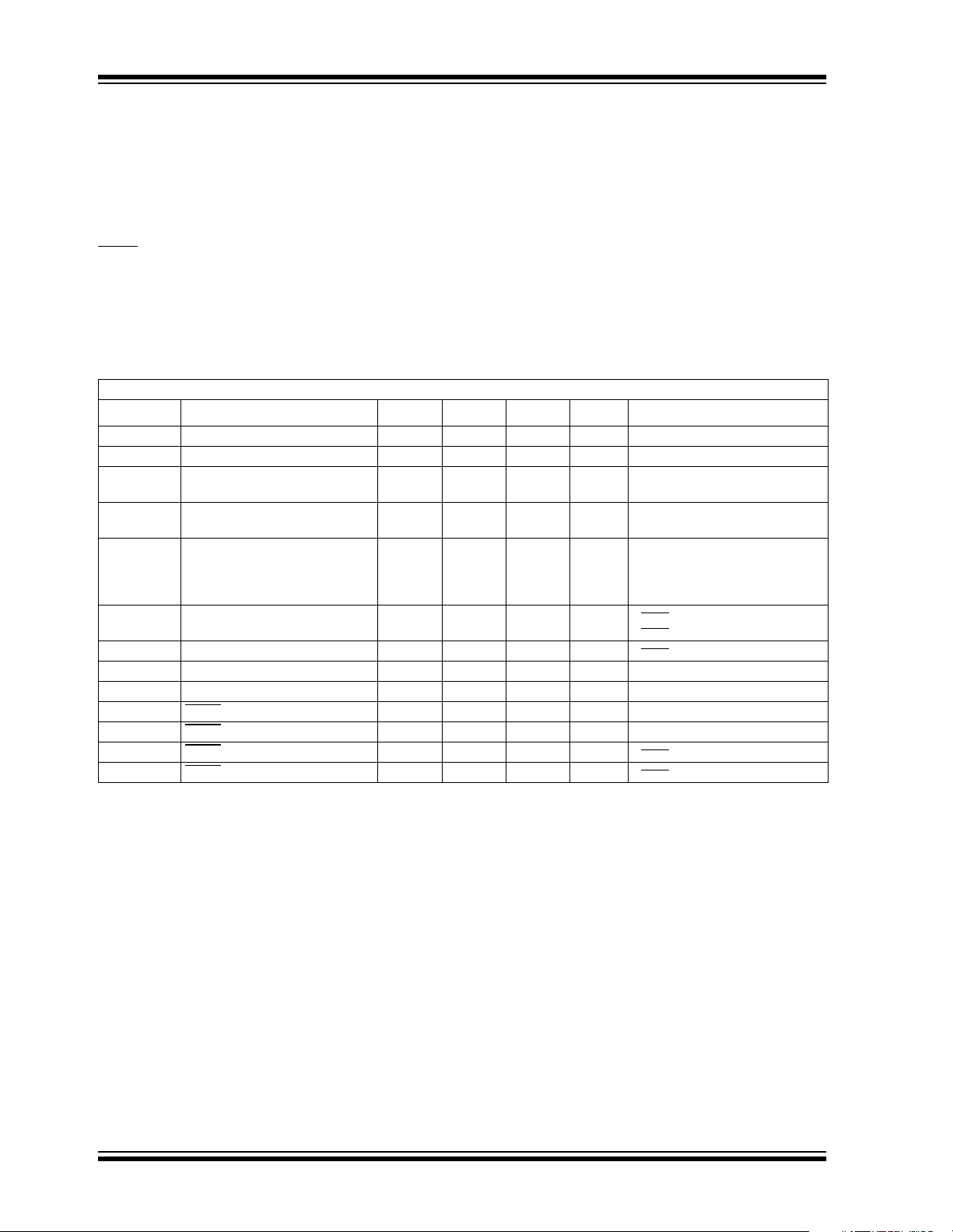
TC56 ELECTRICAL SPECIFICATIONS
Electrical Characteristics: VIN = V
Symbol Parameter Min Typ Max Units Test Conditions
V
IN
V
OUT
I
OUTMAX
∆V
OUT
V
- V
IN
I
DD
I
SHDN
∆V
OUT
∆V
OUT
V
IH
V
IL
I
IH
I
IL
Note 1: VR is the regulator output voltage setting.
Input Voltage ——10 V
Output Voltage 0.98 x VRVR ±0.5% 1.02 x V
Maximum Output Current 150
Load Regulation —
Dropout Voltage —
OUT
Supply Current —
Shutdown Supply Current ——0.1 µAV
/∆VINLine Regulation — 0.2 0.3 %/V I
/∆TV
Temperature Coefficient — ±100 — ppm/°CI
OUT
SHDN Input High Logic Threshold 1.5 ——V
SHDN Input Low Logic Threshold ——0.25 V
SHDN Input Current @V
SHDN Input Current @V
2: Dropout voltage is defined as the input to output differential at which the output voltage drops 2% below its nominal value measured at a
1V differential.
+1V, TA = 25°C, CIN = 4.7µF, C
OUT
180
—
—
—
—
—
IH
IL
——5.0 µAV
-0.2 -0.05 0 µAV
—
—
45
40
200
380
165
330
11
13
= 10µF, unless otherwise noted.
OUT
VI
—
—
90
80
395
770
330
660
19
21
R
mA VR ≥ 2.7V, V
mV 1mA ≤ I
mV I
OUT
V
1mA
OUT
I
OUT
I
OUT
I
OUT
µAV
V
OUT
OUT
= 40mA (Note 1)
= 3V (Note 1)
≥ 4.5V, V
R
OUT
OUT
≤ 80mA, V
OUT
≤ I
≤ 80mA, V
OUT
= 80mA, V
= 5V (Note 1)
OUT
= 160mA, V
= 100mA, V
= 200mA, V
= VIN = 4V
SHDN
= VIN = 6V
SHDN
= GND
SHDN
= 40mA, 4V ≤ VIN ≤ 10V
= 10mA, -40°C < T
= V
SHDN
SHDN
IN
= GND
OUT
OUT
= 3V
= 3V
OUT
= 5V
OUT
= 5V (Note 2)
OUT
< +85°C
J
= 3V
= 5V
DS21436B-page 2 2002 Microchip Technology Inc.
Page 3
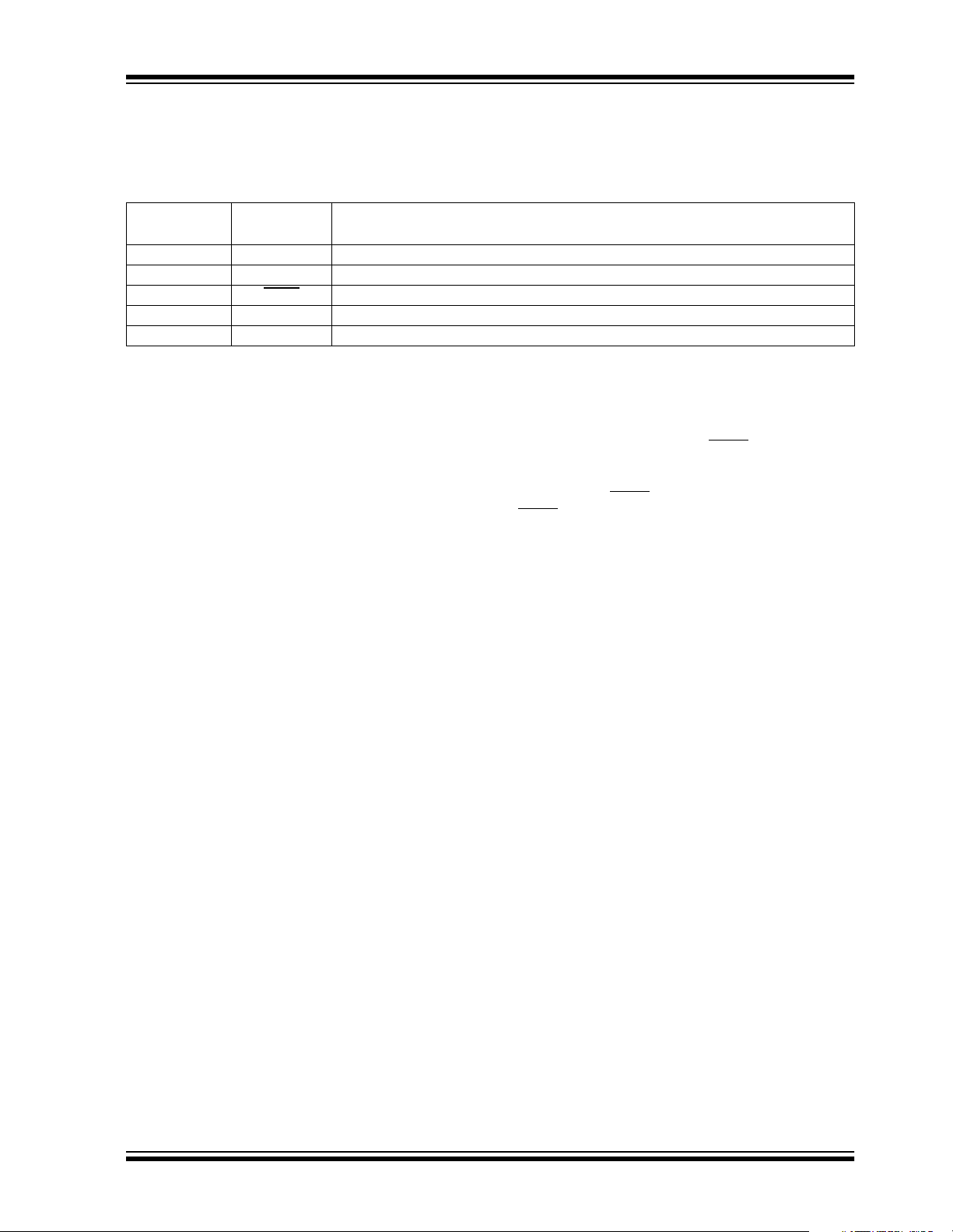
2.0 PIN DESCRIPTIONS
The descriptions of the pins are listed in Table2-1.
TABLE 2-1: PIN FUNCTION TABLE
TC56
Pin No.
(5-Pin SOT-23A)
1V
2V
3SHDN
4 (NC) No connection.
5V
Symbol Description
SS
IN
OUT
Ground.
Supply voltage input.
Shutdown input.
Regulated voltage output.
3.0 DETAILED DESCRIPTION
The TC56 is a precision, fixed output LDO. Unlike
bipolar regulations, the TC56 supply current does not
increase with load current.
3.1 Output Capacitor
A 10µF tantalum capacitor from V
recommended. The output capacitor should have an
effective se ries re sistance greate r than 0.1Ω and less
than 5.0Ω, and a resonant frequency above 1M Hz. It is
recommended that a 4.7µF capacitor be connected
from V
to GND. When operating from sources other
IN
than batteries, supply noise rejection and transient
response can be improved by increasing the value of
the input and output c ap a ci tors and emplo yin g p a ss iv e
filterin g techniques.
to ground is
OUT
3.2 Shutdown Input
The TC56 enters a low power shutdown mode when
the shutdown control input (SHDN
shutdown, the regulator is disabled and supply current
is reduced to 0.1µA (max). Normal operation is
restored when SHDN
input can be tied to VIN.
SHDN
is driven high. If n ot requ ired, th e
) is low. During
2002 Microchip Technology Inc. DS21436B-page 3
Page 4

TC56
4.0 THERMAL CONSIDERATIONS
4.1 Power Dissipation
The amount of power the regulator dissipates is
primarily a function of input and output voltage, and
output current. The following equation is used to
calculate worst case actual power dissipation.
EQUATION 4-1:
PD ≈ (V
Where:
P
= Worst case actual power dissipation
D
= Maximum voltage on V
V
INMAX
V
I
LOADMAX
= Minimum regulator output voltage
OUTMIN
= Maximum output (load) current
The maximum allowable power dissipation
(Equation 4-2) is a function of the maximum ambient
temperature (T
temperature (T
junction-to-air (θ
of approximately 220°C/Watt.
a θ
JA
AMAX
JMAX
JA
EQUATION 4-2:
P
DMAX
Where all terms are previously defined.
– V
INMAX
OUTMIN)ILOADMAX
IN
), the maximum allowable die
) and the thermal resistance from
). The 5-Pin SOT-23A package has
= (T
JMAX
– T
θ
JA
AMAX
)
Equation 4-1 can be used in conjunction with
Equation 4-2 to ensure regulator thermal operation is
within limits. For ex ample:
Given:
V
INMAX
V
OUTMIN
I
LOADMAX
T
JMAX
T
AMAX
=3.0V ±10%
=2.7V – 2%
= 98mA
= 125°C
=55°C
Find: 1. Actual power dissipation
2. Maximum allowable dissipation
Actual power dissipation:
≈ (V
P
D
= [(3.0 x 1.1) – (2.7 x .98)]98 x 10
INMAX
– V
OUTMIN)ILOADMAX
-3
=64mW
Maximum allowable power dissipation:
P
DMAX
= (T
JMAX
– T
θ
JA
AMAX
)
= (125 – 55)
220
= 318mW
In this example, the TC56 dissipates a maximum of
64mW; below the allowab le limit o f 318mW. In a similar
manner , Equation4-1 and Equatio n 4-2 can be used to
calculate maximum current and/or input voltage limits.
4.2 Layout Considerations
The primary path of heat conductio n out of the p ackage
is via the package lea ds. Theref ore, layouts having a
ground plane, wide tra ces at the p ads , and wi de power
supply bus lines combine to lower θ
increase the maximum allowable power dissipation
limit.
and therefore,
JA
DS21436B-page 4 2002 Microchip Technology Inc.
Page 5
TC56
02040
60100
0
OUTPUT CU
I
(mA)
040
80120140180
OUTPUT CU
I
)
U
O
G
)
)
5.1
)
8
9
5.0
0
60100160
OPR
5
C
C
30
C
V
6V
C
4.7
µ
0
µ
)
8
9
3.0
3.1
80
60
80
OPR
5
C
30
C
80
C
V=4V
C
0
µ
5
3.0
3.5
)
)
5
610
V
(V)
84.6
5
5.5
V
(V)
V
(V)
V
(V)
5.0
5.2
)
3.05
85
3
5
0
U
O
G
)
)
95
3.10
5
8
9
85
90
95
5.00
5.05
5.10
6
8
3.0
3.2
3.00
90
6
8
9
OUT
OUT=OUT
m
A
OPR
5
C
C
0
µ
)
OPR
5
C
C
C
µ
OPR
5
C
C
C
µ
OPR
5
C
C
0
µ
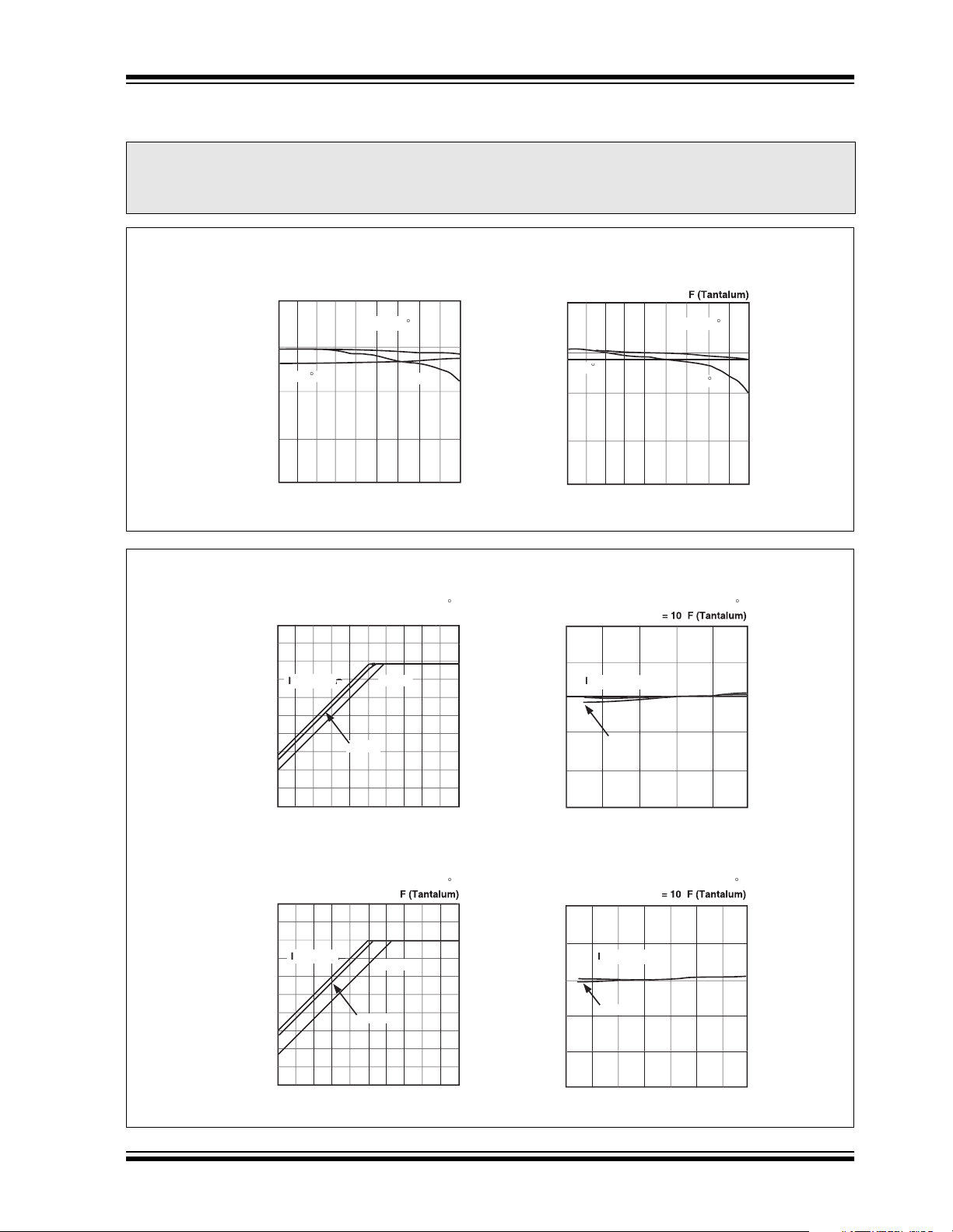
5.0 TYPICAL CHARACTERISTICS
Note: The graphs and tables provided following this note are a statistical summary based on a limited number of
samples and are pro vided for information al purposes only. The perfo rmance characteris tics listed herei n are
not tested or guaranteed. In some graphs or tables, the data presented may be outside the specified
operating range (e.g., outside specified power supply range) and therefore outside the warranted range.
1. OUTPUT VOLTAGE vs. OUTPUT CURRENT
TC565002 (5V
=
F, C = 1
=
F (Tantalum
TC563002 (3V
=µF, C = 1
RRENT
= 2
OUT
80°
(mA
(V)
OUT
-
4.
4.
OUTPUT VOLTAGE V
2
2. OUTPUT VOLTAGE vs. INPUT VOLTAGE
TC565002 (5V)
=µF, C = 1
V
T
4.
OUTPUT VOLTAGE V
4.
INPUT VOLTAGE
10mA
= 2
F (Tantalum
40m
V
T
-
E V
2.
LTA
T V
2.
TP
TC565002 (5V)
=µF,
V
UT
4.
4.
UTPUT VOLTAGE V
4.
= 1mA, 10
40mA
INPUT VOLTAGE
RRENT
= 2
14
1201
OUT
= 2
1
TC563002 (3V
=µF, C = 1
(V)
OUT
2.
2.
OUTPUT VOLTAGE V
=
2.
INPUT VOLTAGE
10mA
40mA
= 2
V
T
E V
LTA
2.
T V
TP
2.
2.
TC563002 (3V
=µF,
= 1mA
OUT
40mA
INPUT VOLTAGE
= 2
1
2002 Microchip Technology Inc. DS21436B-page 5
Page 6

TC56
02040
60100140
OUTPUT CU
I
OU
(mA)
040
80120140180
OUTPUT CU
I
OU
(mA)
U
/OU
U
)
)
0.0
0.2
0.4
0.8
0
60100160
C
30
C
0.0
0.2
0
0.6
0
80120160180
30
C
8
C
0.6
0.8
0
C
µ
0
µ
)
C
µ
0
µ
)
O
)
0
0
V
(V)
)
0.5
0.4
0.3
0.2
0
0
V
(V)
)
0.6
0.7
)
6
8
0.2
0.3
0.4
0.5
0.6
0.7
6
8
80
C
5
C
"
ge
OPR
30
C
"
ge
OPR
30
C
ge
"
ge
0
8
0
)
6
5
6
0
CU
(
)
0
6
0
5.0
0
5
0
8
8
9
O
OPR
80
C
)
V
(V)
6
OPR
80
C
C
5.0 TYPICAL CHARACTERISTICS (CONTINUED)
3. INPUT/OUTPUT VOLTAGE DIFFERENTIAL vs. OUTPUT CURRENT
=
1.
V
F, C = 1
F (Tantalum
1.
V
=
F, C = 1
F (Tantalum
OPR
INPUT/OUTPUT DIFF. V
2
= 25°C
RRENT
80
-
T
T DIFF. V
.4
TP
T
NP
4. SHDN PIN THRESHOLD VOLTAGE vs. INPUT VOLTAGE
TC565002 (5V
V
IL
, V
IH
SHDN PIN THRE. VOL.V
=
2
L" Level Volta
INPUT VOLTAGE
H" Level Volta
1
V
V
L.
HDN PIN THRE. V
= 25°C
OPR
TC563002 (3V
=
25°C
80°C
"L" Level Volta
INPUT VOLTAGE
RRENT
H" Level Volta
-
T
1
IN
5. SUPPLY CURRENT vs. INPUT VOLTAGE
2
TC565002 (5V
A)
(
1
DD
1
SUPPLY CURRENT I
INPUT VOLTAGE
-30°C
1
=
25
1
RRENT I
1
PPLY
TC565002 (5V
=
25°C
-30°C
1
INPUT VOLTAGE V(V
DS21436B-page 6 2002 Microchip Technology Inc.
Page 7

5.0 TYPICAL CHARACTERISTICS (CONTINU ED)
CU
I
3
5
0
V
(V)
)
5
0
5.0
0
0
0
V
(V)
)
0
)
6
8
9
6.0
8.0
0
6
5
C
8
C
30
C
5
C
6
C
80
C
020
OPR
(C)
0
040
80
OPR
)
U
O
G
V
)
)
5.10
)
90
95
5.00
5.05
020
60
90
95
3.00
3.05
3.10
0406080
A
A
OUT
A
A
6V
C
0
µ
)
C
0
µ
02080
CU
)
0
8.0
0
0
80
O
(
C)
)
6
0
6V
6.0
8.0
0
16
02040
60
OPR
(C)
0
040
60
5. SUPPLY CURRENT vs. INPUT VOLTAGE (CONT.)
TC56
2
A
1
80°
1
-
SUPPLY CURRENT I
INPUT VOLTAGE
2
1
6. OUTPUT VOLTAGE vs. AMBIENT TEMPERATURE
TC563002 (3V
TC565002 (5V
=µF, C = 1
(V)
OUT
4.
OUTPUT VOLTAGE V
I
OUT
=
F (Tantalum
= 10m
40m
1
RRENT
1
PPLY
V
T
E
LTA
T V
2.
TP
TC563002 (3V
-30°
INPUT VOLTAGE
TC563002 (3V
=µF, C = 1
I
2
1
=
= 10m
40m
4.
-4
-2
(C
2.
-40-2
7. SUPPLY CURRENT vs. AMBIENT TEMPERATURE
TC565002 (5V
1
1
SUPPLY CURRENT I
6.
-4
-2
=
RRENT I
1
PPLY
-4
PR
2002 Microchip Technology Inc. DS21436B-page 7
-2
TC563002 (3V
=
Page 8

TC56
)
)
)
)
)
0
2
8
6
6
8
)
)
0
8
6
6
8
)
U
O
G
)
0
6
6
)
)
0
6
6
3
5
6
8
0
3
5
6
8
7
0
5
3
0
6
5
3
0
6
I
ge
ge
)V)
U
O
G
)
U
O
G
)
OUT
0
µ
)
ge
ge
ge
O
e
OUT
0
µ
)
OUT
0
µ
)
O
ge
OUT
0
µ
)
)
3
5
6
8
)
U
O
G
)
)
)
3
5
6
8
9
5.0
5.1
5.2
5.3
5.4
9
5.0
5.1
5.2
5.3
5.4
U
O
G
)
ge
O
ge
ge
O
ge
OUT
0
µ
)
OUT
0
µ
)
5.0 TYPICAL CHARACTERISTICS (CONTINUED)
8. INPUT TRANSIENT RESPONSE 1
= 1mA, C = 1
F (Tantalum
TC565002 (5V
= 10mA, C = 1
F (Tantalum
V
-
-
INPUT VOLTAGE V
-
-
nput Volta
TIME: (0.1 msec/div
TC563002 (3V
= 1mA, C = 1
V
INPUT VOLTAGE V
Input Volta
Output Volta
F (Tantalum
utput Voltag
V
T
V
T
E V
LTA
T V
TP
V
-
-
-
-
Input Volta
Output Volta
TIME: (0.1 msec/div
V
T
E V
LTA
T V
TP
TC563002 (3V
= 10mA, C = 1
Input Voltage
F (Tantalum
utput Volta
V
T
E V
LTA
T V
TP
TIME: (0.1 msec/div
TIME: (0.1 msec/div
9. INPUT TRANSIENT RESPONSE 2
TC565002 (5V
= 1mA, C = 1
Input Volta
V
INPUT VOLTAGE V
TIME: (0.1 msec/div
DS21436B-page 8 2002 Microchip Technology Inc.
F (Tantalum
utput Volta
= 10mA, C = 1
V
T
E V
LTA
T V
TP
4.
V
E V
LTA
T V
NP
Input Volta
TIME: (0.1 msec/div
F (Tantalum
(V)
OUT
utput Volta
OUTPUT VOLTAGE V
4.
Page 9

5.0 TYPICAL CHARACTERISTICS (CONTINU ED)
)
)
U
O
G
)
U
O
G
)
)
)
5
3
0
6
3.15
3.10
3.05
90
3.20
3.00
95
)
5
3
0
6
3.15
3.10
3.05
90
3.20
3.00
95
ge
ge
O
ge
OUT
0
µ
)
OUT
0
µ
)
)
U
CU
)
U
O
G
)
)
0
µ
)
3.1
3.0
9
6
3.2
8
0
µ
)
5.1
5.0
9
6
5.2
8
00
60
0
0
0
0
0
200
60
120
0
240
80
0
40mA Output Current
t
O
ge
40mA Output Current
t
O
ge
)
)
)
)
)
U
O
G
)
6V
OUT
0
µ
)
6V
OUT
A
, C
0
µ
)
3
5
6
8
035
6
8
0
5V
5V
O
ge
5V
O
ge
9. INPUT TRANSIENT RESPONSE 2 (CONT.)
TC563002 (3V
= 1mA, C = 1
F (Tantalum
TC563002 (3V
= 10mA, C = 1
TC56
F (Tantalum
Input Volta
V
E V
LTA
T V
NP
Output Voltage
TIME (1 msec/div
10. LOAD TRANSIENT RESPONSE
= 6V, C = 1
(V)
T
4.
4.
OUTPUT VOLTAGE V
4.
0mA Output Curren
TIME (2 msec/div
utput Volta
F (Tantalum
V
V
T
E V
LTA
T V
TP
2.
2.
24
mA
T
RRENT I
T
TP
V
UT
E V
LTA
T V
TP
2.
2.
2.
2
1
12
8
4
Input Volta
utput Volta
TIME (1 msec/div
= 4V, C = 1
utput Volta
0mA Output Curren
TIME (2 msec/div
F (Tantalum
2.
2.
(mA)
OUT
1
4
OUTPUT CURRENT I
(V)
OUT
OUTPUT VOLTAGE V
11. SHDN PIN TRANSIENT RESPONSE
TC565002 (5V
= 1mA, C = 1
= 1.
V
T
= 0.2
OUTPUT VOLTAGE V
TIME (0.1 msec/div
utput Volta
=
F (Tantalum
V
T
E V
LTA
T V
TP
2002 Microchip Technology Inc. DS21436B-page 9
TC565002 (5V
= 10m
= 0.2
TIME (0.1 msec/div
= 1
F (Tantalum
utput Volta
=
Page 10

TC56
)
)
)
)
)
U
O
G
)
5
3
0
6
5
3
0
6
SHDN Pin Input Voltage
ge
Outp
t
Outp
t
SHDN Pin Input Voltage
ge
OUT
0
µ
)
OUT
A
, C
0
µ
)
5V
5V
5V
(
)
)
30
0
50
60
80
0
0
0
0
)
30
0
50
60
80
0
0
0
0
0.01
0.1
0
0.01
0.1
0
C
p
p
C
OUT
A
,
µ
6V
C
p
p
C
OUT
A
,
C
µ
5.0 TYPICAL CHARACTERISTICS (CONTINUED)
11. SHDN PIN TRANSIENT RESPONSE (CONT.)
TC563002 (3V
= 1mA, C = 1
=
F (Tantalum
TC563002 (3V
= 10m
= 1
=
F (Tantalum
V
T
OUTPUT VOLTAGE V
= 1.
HDN Pin Input Volta
= 0.2
ut Curren
TIME: (0.1 msec/div
12. RIPPLE REJECTION RATE
= 40m
dB
7
4
V
T
E V
LTA
T V
TP
= 1.
HDN Pin Input Volta
= 0.25V
ut Curren
TIME: (0.1 msec/div
TC563002 (3V)TC565002 (5V)
D
A
7
4
= 40m
=
D
A
2
1
IPPLE REJECTION RATE RR
1
RIPPLE FREQUENCY f (kHz
2
1
1
RIPPLE FREQUENCY f (kHz
DS21436B-page 10 2002 Microchip Technology Inc.
Page 11

6.0 PACKAGING INFORMATION
TC56
6.1 Package Marking Information
3
1
represents the integer of the output voltage
Symbol Voltage
A0.
B1.
C2.
D3.
E4.
F5.
H6.
6.2 Taping Form
2
represents the integer of the output voltage
Symbol Voltage Symbol Voltage
A.0F.5
B.1H.6
C.2K.7
D.3L.8
E.4M.9
3
represents the transition response
Symbol
— REGULAR
4
represents assembly lot code
Component Taping Orientation for 5-Pin SOT-23A (EIAJ SC-74A) Devices
User Direction of Feed
Device
Marking
W
PIN 1
Standard Reel Component Orientation
TR Suffix Device
(Mark Right Side Up)
Carrier Tape, Number of Components Per Reel and Reel Size
Package Carrier Width (W) Pitch (P) Part Per Full Reel Reel Size
5-Pin SOT-23A 8 mm 4 mm 3000 7 in
P
2002 Microchip Technology Inc. DS21436B-page 11
Page 12

TC56
6.3 Package Dimensions
SOT-23A-5
.075 (1.90)
REF.
.122 (3.10)
.098 (2.50)
.020 (0.50)
.012 (0.30)
.057 (1.45)
.035 (0.90)
PIN 1
.006 (0.15)
.000 (0.00)
.122 (3.10)
.106 (2.70)
.071 (1.80)
.059 (1.50)
.037 (0.95)
REF.
10° MAX.
.010 (0.25)
.004 (0.09)
.024 (0.60)
.004 (0.10)
Dimensions: inches (mm)
DS21436B-page 12 2002 Microchip Technology Inc.
Page 13

TC56
Sales and Support
Data Sheets
Products supported by a preliminary Data Sheet may have an errata sheet describing minor operational differences and recommended workarounds. To determine if an errata sheet exists for a particular device, please contact one of the following:
1. Your local Microchip sales office
2. The Microchip Corporate Literature Center U.S. FAX: (480) 792-7277
3. The Microchip Worldwide Site (www.microchip.com)
Please specify which device, revision of silicon and Data Sheet (include Literature #) you are using.
New Customer Notification System
Register on our web site (www.microchip.com/cn) to receive the most current information on our products.
2002 Microchip Technology Inc. DS21436B-page13
Page 14

TC56
NOTES:
DS21436B-page14 2002 Microchip Technology Inc.
Page 15

TC56
Information contained in this publication regarding device
applications and the like is intended through suggestion only
and may be superseded by updates. It is your responsibility to
ensure that your application meets with your specifications.
No representation or warranty is given and no liability is
assumed by Microchip Technology Incorporated with respect
to the accuracy or use of such information, or infringement of
patents or other intellectual property rights arising from such
use or otherwise. Use of Microchip’s products as critical components in life support systems is not authorized except with
express written approval by Microchip. No licenses are conveyed, implicitly or otherwise, under any intellectual property
rights.
Trademarks
The Microchip name and logo, the Microchip logo, FilterLab,
EELOQ, microID, MPLAB, PIC, PICmicro, PICMASTER,
K
PICSTART, PRO MATE, SEEVAL and The Embedded Control
Solutions Company are registered trademarks of Microchip Technology Incorporated in the U.S.A. and other countries.
dsPIC, ECONOMONITOR, FanSense, FlexROM, fuzzyLAB,
In-Circuit Serial Programming, ICSP, ICEPIC, microPort,
Migratable Memory, MPASM, MPLIB, MPLINK, MPSIM,
MXDEV , MXLAB, PICC , PICDEM, PICDEM.net, rfP IC, Select
Mode and Total Endurance are trademarks of Microchip
Technology Incorporated in the U.S.A.
Serialized Quick Turn Programming (SQTP) is a service mark
of Microchip Technology Incorporated in the U.S.A.
All other trademarks mentioned herein are property of their
respective companies.
© 2002, Microchip Technology Incorporated, Printed in the
U.S.A., All Rights Reserved.
Printed on recycled paper.
Microchip received QS-9000 quality system
certification for its worldwide headquarters,
design and wafer fabrication facilities in
Chandler and Tempe, Arizona in July 1999
and Mountain View, California in March 2002.
The Company’s quality system processes and
procedures are QS-9000 compliant for its
PICmicro
devices, Serial EEPROMs, micrope ri ph era ls,
non-volatile memory and ana l og pro duc ts. In
addition, Microchip’s quality system for the
design and manufacture of development
systems is ISO 9001 certified.
®
8-bit MCUs, KEELOQ
®
code hoppin g
2002 Microchip Technology Inc. DS21436B-page 15
Page 16

M
WORLDWIDE SALES AND SERVICE
AMERICAS
Corporate Office
2355 West Chandler Blvd.
Chandler, AZ 85224-6199
Tel: 480-792-7200 Fax: 480-792-7277
Technical Support: 480-792-7627
Web Address: http://www.microchip.com
Rocky Mountain
2355 West Chandler Blvd.
Chandler, AZ 85224-6199
Tel: 480-792-7966 Fax: 480-792-7456
Atlanta
500 Sugar Mill Road, Suite 200B
Atlanta, GA 30350
Tel: 770-640-003 4 Fax: 770-640-0307
Boston
2 Lan Drive, Suite 120
Westford, MA 01886
Tel: 978-692-384 8 Fax: 978-692-3821
Chicago
333 Pierce Road, Suite 180
Itasca, IL 60143
Tel: 630-285-0071 Fax: 630-285-0075
Dallas
4570 Westgrove Drive, Suite 160
Addison, TX 75001
Tel: 972-818-742 3 Fax: 972-818-2924
Detroit
Tri-Atria Office Building
32255 Northwestern Highway, Suite 190
Farmington Hills, MI 48334
Tel: 248-538-2250 Fax: 248-538-2260
Kokomo
2767 S. Albright Road
Kokomo, Indiana 46902
Tel: 765-864-8360 Fax: 765-864-8387
Los Angeles
18201 Von Karman, Suite 1090
Irvine, CA 92612
Tel: 949-263-188 8 Fax: 949-263-1338
New York
150 Motor Parkway, Suite 202
Hauppauge, NY 11788
Tel: 631-273-530 5 Fax: 631-273-5335
San Jose
Microchip Technology Inc.
2107 North First Street, Suite 590
San Jose, CA 95131
Tel: 408-436-795 0 Fax: 408-436-7955
Toronto
6285 Northam Drive, Suite 108
Mississauga, Ontario L4V 1X5, Cana da
Tel: 905-673-0699 Fax: 905-673-6509
ASIA/PACIFIC
Australia
Microchip Technology Australia Pty Ltd
Suite 22, 41 Rawson Street
Epping 2121, NSW
Australia
Tel: 61-2-9868-6733 Fax: 61-2-9868-6755
China - Beij ing
Microchip Technology Consulting (Shanghai)
Co., Ltd., Beijing Liaison Office
Unit 915
Bei Hai Wan Tai Bldg.
No. 6 Chaoyangmen Beidajie
Beijing, 100027, No. China
Tel: 86-10-85282100 Fax: 86-10-85282104
China - Chengdu
Microchip Technology Consulting (Shanghai)
Co., Ltd., Chengdu Liaison Office
Rm. 2401, 24th Floor,
Ming Xing Financial Tower
No. 88 TIDU Street
Chengdu 610016, China
Tel: 86-28-86766200 Fax: 86-28-86766599
China - Fuzhou
Microchip Technology Consulting (Shanghai)
Co., Ltd., Fuzhou Liaison Office
Unit 28F, World Trade Plaza
No. 71 Wusi Road
Fuzhou 350001, China
Tel: 86-591-7503506 Fax: 86-591-7503521
China - Shanghai
Microchip Technology Consulting (Shanghai)
Co., Ltd.
Room 701, Bldg. B
Far East International Pla za
No. 317 Xian Xia Road
Shanghai, 200051
Tel: 86-21-6275-5700 Fax: 86-21-6275-5060
China - Shenzhen
Microchip Technology Consulting (Shanghai)
Co., Ltd., Shenzhen Liaison Office
Rm. 1315, 13/F, Shenzhen Kerry Centre,
Renminnan Lu
Shenzhen 518001, China
Tel: 86-755-2350361 Fax: 86-755-2366086
China - Hong Kong SAR
Microchip Technology Hongkong Ltd.
Unit 901-6, Tower 2, Metroplaza
223 Hing Fong Road
Kwai Fong, N.T., Hong Kong
Tel: 852-2401-1200 Fax: 852-2401-3431
India
Microchip Technology Inc.
India Liaison Office
Divyasree Chambers
1 Floor, Wing A (A3/A4 )
No. 11, O’Shaugnessey Road
Bangalore, 560 025, India
Tel: 91-80-2290061 Fax: 91-80-2290062
Japan
Microchip Technology Japan K.K.
Benex S-1 6F
3-18-20, Shinyokohama
Kohoku-Ku, Yokohama-shi
Kanagawa, 222-0033, Japan
Tel: 81-45-471- 6166 Fax: 81-45-471-6122
Korea
Microchip Technology Korea
168-1, Youngbo Bldg. 3 Floor
Samsung-Dong, Kangnam-Ku
Seoul, Korea 135-882
Tel: 82-2-554-7200 Fax: 82-2-558-5934
Singapore
Microchip Technology Singapore Pte Ltd.
200 Middle Road
#07-02 Prime Centre
Singapore, 188980
Tel: 65-6334-8870 Fax: 65-6334-8850
Taiwan
Microchip Technology Taiwan
11F-3, N o. 207
Tung Hua North Road
Taipei, 105, Taiwan
Tel: 886-2-2717-7175 Fax: 886-2-2545-0139
EUROPE
Denmark
Microchip Technology Nordic ApS
Regus Business Centre
Lautrup hoj 1-3
Ballerup DK-2750 Denmark
Tel: 45 4420 9895 Fax: 45 4420 9910
France
Microchip Technology SARL
Parc d’Activite du Moulin de Massy
43 Rue du Saule Trapu
Batiment A - ler Etage
91300 Massy, France
Tel: 33-1-69-53-63-20 Fax: 33-1-69-30-90-79
Germany
Microchip Technology GmbH
Gustav-Heinemann Ring 125
D-81739 Munich, Germany
Tel: 49-89-627-144 0 Fax: 49-89-627-144-44
Italy
Microchip Technology SRL
Centro Direzionale Colleoni
Palazzo Taurus 1 V. Le Colleoni 1
20041 Agrate Brianza
Milan, Italy
Tel: 39-039-65791-1 Fax: 39-039-6899883
United Kingdom
Microchip Ltd.
505 Eskdale Road
Winnersh Triangle
Wokingham
Berkshire, England RG41 5TU
Tel: 44 118 921 5869 Fax: 44-118 921-5820
05/01/02
'! #'
DS21436B-page 16 2002 Microchip Technology Inc.
 Loading...