

TC530/TC534
5V Precision Data Acquisition Subsystems
Features
• Precision (up to 17-Bits) A/D Converter
•3-WireSerialPort
• Flexible:User Can TradeOff Conversion Speed For
Resolution
• Single Supply Operation
•-5VOutputPin
• 4 Input, Differential Analog MUX (TC534)
• Automatic Input Polarity and Overrange Detection
• Low Operating Current: 5mA Max
• Wide Analog Input Range: ±4.2V Max
• Cost Effective
Applications
• Precision Analog Signal Processor
• PrecisionSensor Interface
• High Accuracy DC Measurements
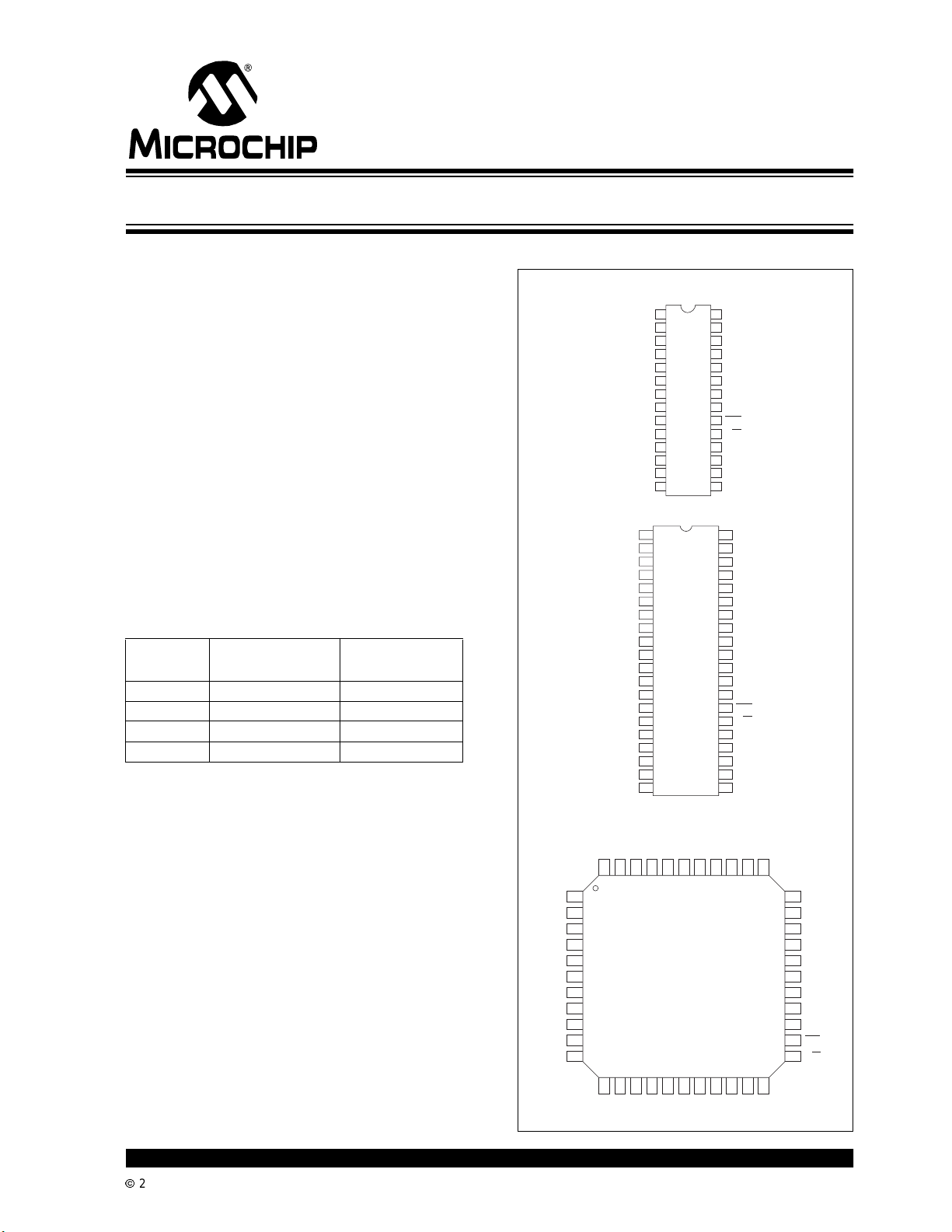
Device Selection Table
Part Number Package
TC530COI 28-PinSOIC 0°C to +70°C
TC530CPJ 28-PinPDIP(Narrow) 0°C to +70°C
TC534CKW 44-PinPQFP 0°C to +70°C
TC534CPL 40-Pin PDIP 0°C to +70°C
Temperature
Range
Package Types
ACOM
C
V
OSC
V
SS
C
INT
C
AZ
BUF
ACOM
C
REF
C
REF
V
REF
V
REF
CH4-
CH3-
CH2-
CH1-
CH4+
CH3+
CH2+
CH1+
DGND
A1
A0
V
C
C
BUF
C
REF
REF
V
REF
REF
VIN-
V
DGND
N/C
OUT
-
+
-
+
SS
INT
AZ
IN
10
11
12
13
14
15
16
17
18
19
20
28-Pin SOIC
28-Pin PDIP
1
2
3
4
5
-
6
TC530CPI
+
7
TC530COI
-
8
+
9
10
+
11
12
13
14
40-Pin PDIP
1
2
3
4
5
6
7
8
9
TC534CPL
28
27
26
25
24
23
22
21
20
19
18
17
16
15
CAP-
AGND
CAP+
V
NC
OSC
V
RESET
EOC
R/W
D
D
D
OSC
40
39
38
37
36
35
34
33
32
31
30
29
28
27
26
25
24
23
22
21
DD
CCD
IN
CLK
OUT
CAP-
AGND
CAP+
V
N/C
N/C
OSC
N/C
V
N/C
RESET
N/C
N/C
EOC
R/W
D
D
D
OSC
OSC
IN
DD
CCD
IN
CLK
OUT
IN
OUT
44-Pin PQFP
INT
A1
DGND
CAP-
NC
394041424344
38 37 36 35 34
A0
NC
BUF
CAZVSSC
1
NC
2
ACOM
C
-
3
REF
C
+
4
REF
V
-
5
REF
V
+
6
REF
7
CH4-
CH3-
8
CH2-
9
CH1-
10
CH4+
11
12 13 14 15 16 17 18 19 20 21 22
CH3+
2002 Microchip TechnologyInc. DS21433B-page 1
CH2+
TC534CKW
CH1+
OUT
OSC
AGND
IN
OSC
CAP+
OUT
D
DD
NC
V
NC
33
OSC
32
NC
31
V
30
CDD
NC
29
RESET
28
NC
27
26
NC
NC
25
24
EOC
23
R/W
IN
D
CLK
D
TC530/TC534
p
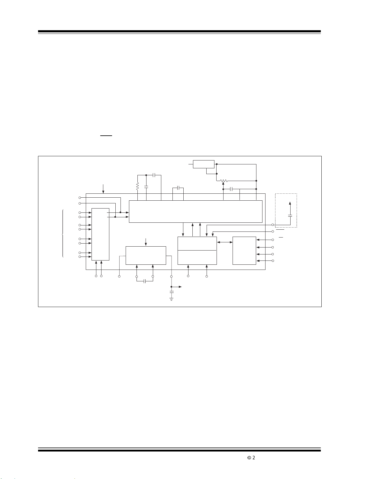
General Description
The TC530/TC534 are serial analog data acquisition
subsystems ideal for high precisionmeasurements(up
to 17-bits plus sign). The TC530 consists of a dual
slope integrating A/D converter, negative power supply generator and 3 wire serial interface port. The
TC534 is identical to the TC530, but adds a four channel differential input multiplexer. Key A/D converter
operating parameters (Auto Zero and Integration time)
are programmable, allowing the user to trade
conversion time for resolution.
Data conversion is initiated when the RESET input is
brought low. After conversion, data is loaded into the
output shift register and EOC
is asserted, indicating
Typical Application
C
(TC530 Only)
TC534
(Only)
VIN-
VIN+
CH1+
CH1-
CH2+
CH2-
CH3+
CH3-
CH4+
CH4-
+5V
DIF.
MUX
(TC534
Only)
V
DD
R
TC530
TC534
INT
BUF
IN+
IN-
DC-TO-DC
C
AZ
V
DD
Converter
INT
C
AZ
INT
new data is available. The converted data (plus Overrange and polarity bits) is held in the output shift register until read by the processor or until the next
conversion is completed, allowing the user to access
data at any time.
The TC530/TC534 timebase can be der ived from an
external crystal of 2MHz (max) or from an external frequencysource.TheTC530/TC534requiresasingle5V
power supply and features a -5V, 10mA output which
can be used to supply negative bias to other
components in the system.
V
MCP1525
DD
C
REF
C
+
REF
CMPTR
-
AB
State
Machine
Oscillator
(÷ 4)
C
REF
Dual Slope A/D Converter
100k
REF
.01µF
+
V
-V
REF
Serial Port
ACOM
0.01µF
RESET
EOC
R/W
D
IN
D
OUT
D
CLK
V
DD
Optional
Power-On
Reset Ca
A0 A1
OSC
CAP+
CAP–
V
SS
OSC
Negative
Supply Output
OSC
IN
OUT
DS21433B-page 2
2002 Microchip TechnologyInc.
TC530/TC534
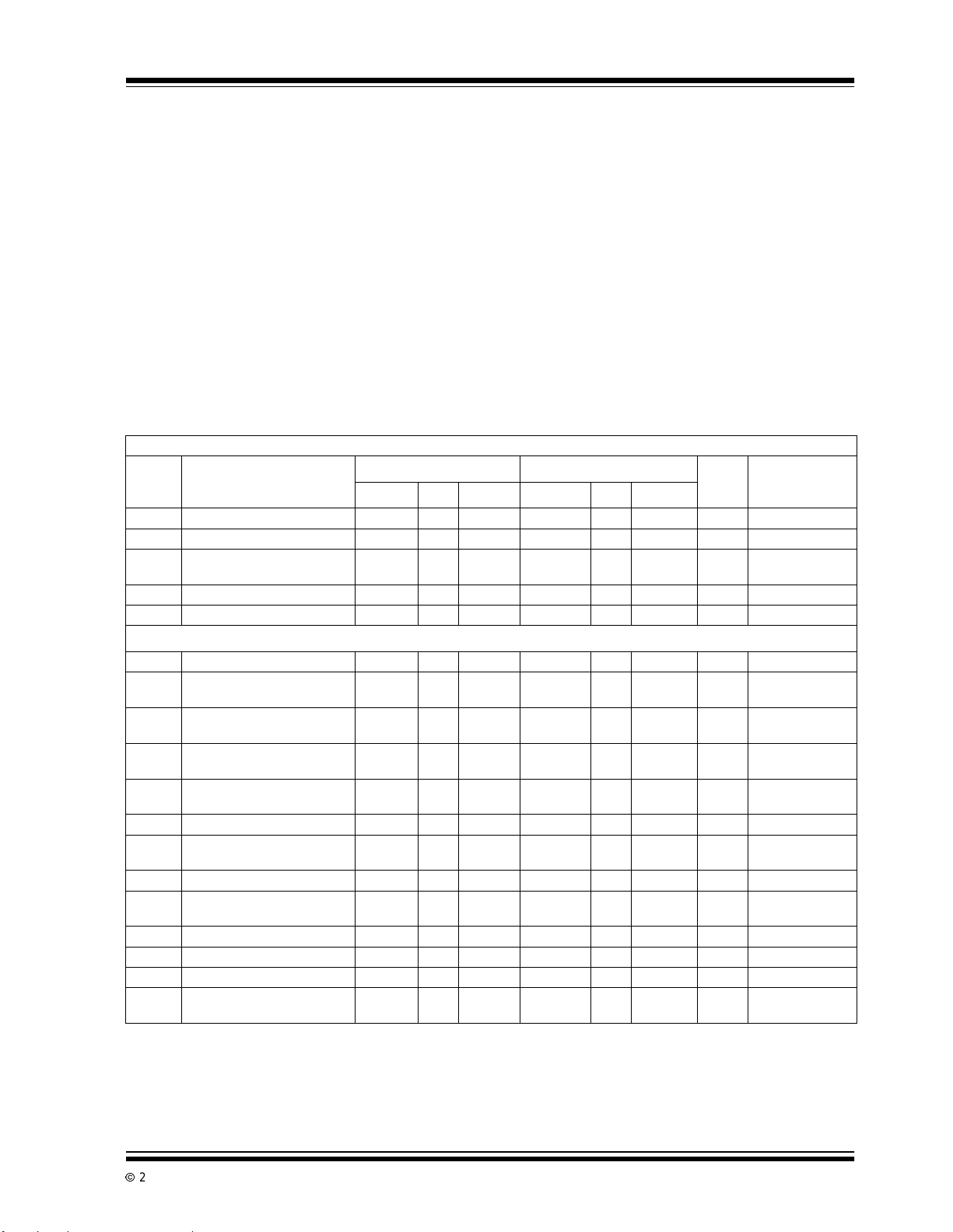
1.0 ELECTRICAL
CHARACTERISTICS
*Stresses above those listed under "Absolute Maximum Ratings"maycause permanentdamage to thedevice.These are
stress ratings only and functional operation of the device at
these or any other conditions above those indicated in the
Absolute Maximum Ratings*
Supply Voltage ......................................................+6V
Analog Input Voltage(V
+orVIN-).............VDDtoV
IN
SS
operation sections of the specifications is not implied. Exposure to Absolute Maximum Rating conditions for extended
periodsmay affectdevice reliability.
Logic Input Voltage.........(VDD+ 0.3V) to (GND - 0.3V)
Ambient Operating Temperature Range:
PDIP Package (C)................. 0°C to +70°C
SOIC Package (C) ................ 0°C to +70°C
PQFP Package (C) ............... 0°C to +70°C
StorageTemperature Range..............-65°C to +150°C
TC530/TC530A/T C534 ELECTRICAL SPECIFICATIONS
Electrical Characteristics: VDD=V
CCD,CAZ=CREF
Symbol Parameter
Min Typ Max Min Typ Max
Analog Power Supply Voltage 4.5 5.0 5.5 4.5 — 5.5 V
V
DD
V
Digital Power Supply Voltage 4.5 5.0 5.5 4.5 — 5.5 V
CCD
TC530/TC534 Total Power
P
D
Dissipation
Supply Current (VS+PIN)—1.82.5——3.0mA
I
S
I
CCD
Supply Current (V
)——1.5 ——1.7mAF
CCDPIN
——25 — ——mΩ VDD=V
Analog
R Resolution — — ±17 — — ±17 Bits Note 1
ZSE Zero Scale Error with Auto
— — 0.5 — 0.005 0.012 % F.S.
ZeroPhase
ENL End Point Linearity — 0.015 0.030 — 0.015 0.045 % F.S. Note 1 and
NL Max. Deviation from Best
— 0.008 0.015 — — — % F.S. Note 1 and
Straight Line Fit
ZS
Zero Scale Temperature
TC
Coefficient
——— — 1 2µV/°C
SYE Rollover Error — .012 — — .03 — %F.S. Note 3
FS
V
V
Full Scale Temperature
TC
Coefficient
Input Current — 6 — — — — pA VIN=0V
I
IN
Common-Mode Voltage
CMR
Range
Integrator Output Swing VSS+0.9 — VDD-0.9 VSS+0.9 — VDD-0.9 V
V
INT
Analog Input Signal Range VSS+1.5 — VDD-1.5 VSS+1.5 — VDD-1.5 V
V
IN
VoltageReference Range VSS+1 — VDD-1 VDD+1 — VDD-1 V
REF
Zero Crossing
T
D
Comparator Delay
— — — — 10 — ppm/°CExt. V
VSS+1.5 — VDD-1.5 VSS+1.5 — VDD-1.5 V
—2.0— — 3.0—µsec
Note 1: Integrate time ≥ 66msec, Auto Zero time ≥ 66msec, V
2: End point linearity at ±1/4, ±1/2 ±3/4, F.S. after full scale adjustment.
3: Rollover error is relatedto capacitor used for C
4: TC534 Only.
=0.47µF, unless otherwise specified.
=+25°C TA=0°Cto+70°C
T
A
(pk) = 4V.
INT
. See Table 5-2, Recommended Capacitor for C
INT
Unit Test Conditions
OSC
Note 2
Note 2
T.C. = 0ppm/°C
.
INT
CCD
=1MHz
REF
=5V
2002 Microchip TechnologyInc. DS21433B-page 3
TC530/TC534
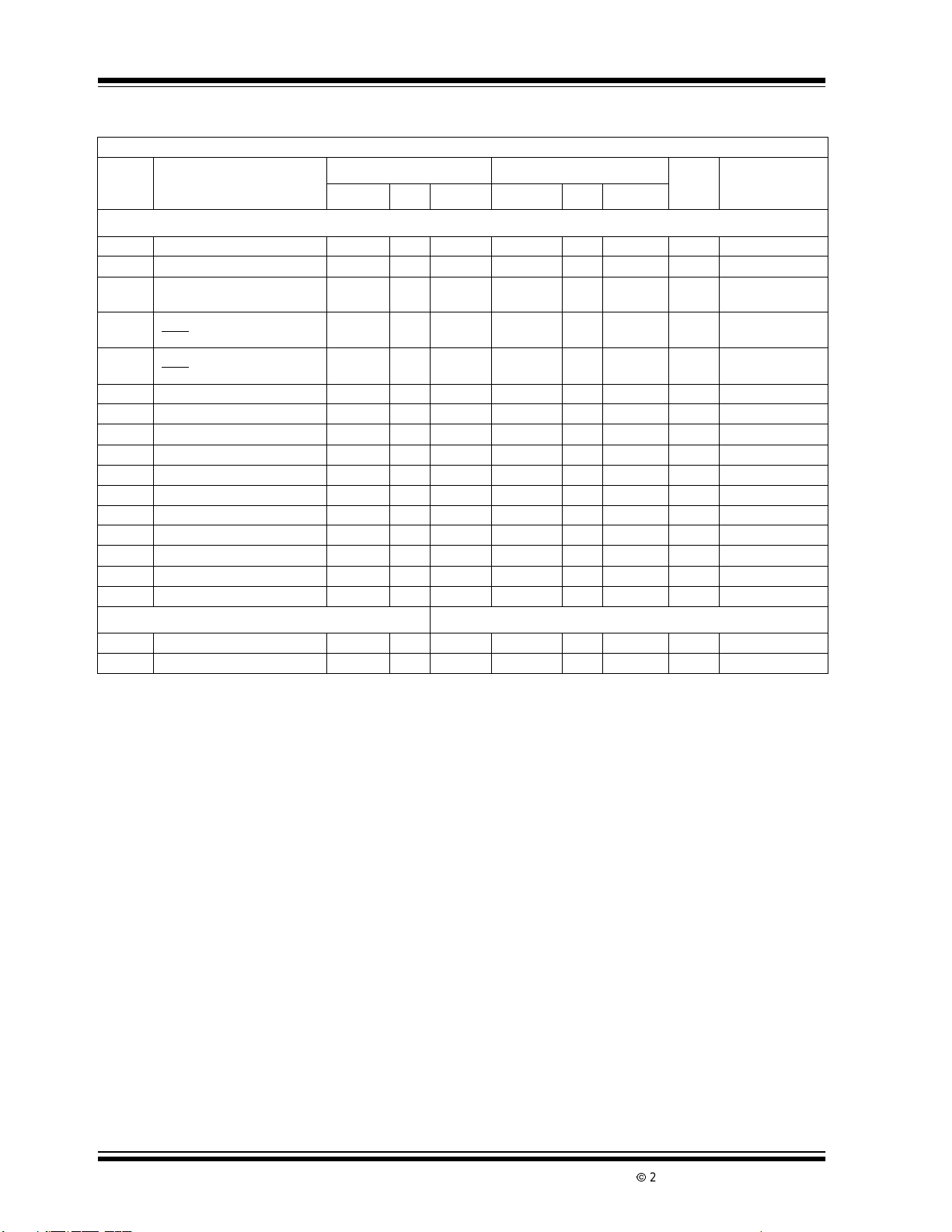
TC530/TC530A/T C534 ELECTRICAL SPECIFICATIONS (CONTINUED)
Electrical Characteristics: VDD=V
Symbol Parameter
CCD,CAZ=CREF
=0.47µF , unless otherwise specified.
=+25°C TA=0°Cto+70°C
T
A
Min Typ Max Min Typ Max
Serial Port Interface
V
Input LogicHIGHLevel 2.5 — — 2.5 — — V
IH
Input LogicLOW Level — — 0.8 — — 0.8 V
V
IL
I
IN
V
OL
T
R,TF
F
XTL
F
EXT
T
RS
T
RD
T
DRSDCLK
T
PWLDCLK
T
PWHDCLK
T
DR
R
OUT
F
CLK
I
OUTVSS
Input Current
(DI, DO, D
CLK
)
LogicLOW Output Voltage
(EOC
)
Rise and Fall Times
(EOC
,DI,DO)
Crystal Frequency — — 2.0 — —2.0MHz
External Frequency on OSC
Read Setup Time 1 — — — 1 — µsec
Read Delay Time 250 — — — 250 nsec
to D
Delay 450 — — — 450 nsec
OUT
LOW Pulse Width 150 — — — 150 nsec
HIGH Pulse Width 150 — — — 150 nsec
Data Ready Delay 200 — — — 200 nsec
OutputResistance — 65 85 — — 100 Ω I
Oscillator Frequency — 100 — — — — kHz C
Output Current — — 10 — — 10 mA
——10 — — — µA
— 0.2 0.3 — — 0.35 V I
——250 — 250 nsecC
——4.0 — —4.0MHz
IN
Multiplexer
V
R
MaximumInputVoltage -2.5 — 2.5 -2.5 — 2.5 V
IMMAX
Drain/Source ON Resistance — 6 10 — — — kΩ
DSON
Note 1: Integrate time ≥ 66msec, Auto Zero time ≥ 66msec, V
2: End point linearity at ±1/4, ±1/2 ±3/4, F.S. after full scale adjustment.
3: Rollover error is relatedto capacitor used for C
4: TC534 Only.
. See Table 5-2, Recommended Capacitor for C
INT
(pk) = 4V.
INT
Unit Test Conditions
=250µA
OUT
=10pF
L
=10mA
OUT
=0
OSC
.
INT
DS21433B-page 4
2002 Microchip TechnologyInc.
TC530/TC534
2.0 PIN DESCRIPTIONS
ThedescriptionsofthepinsarelistedinTable2-1
TABLE 2-1: PIN FUNCTION TABLE
Pin Number
(TC530)
28-Pin PDIP
Pin Number
(TC530)
28-Pin SOIC
Pin Number
(TC534)
40-PinPDIP
11 140V
22 241C
33 342C
4 4 4 43 BUF Analog output. Integrator capacitor connection and voltage
5 5 5 2 ACOM Analog input. This pin is ground for all of the analog
66 6 3C
77 7 4C
88 8 5V
99 9 6V
Not Used Not Used 10 7 CH4- A nalog Input. Multiplexer channel4 negative differential
Not Used Not Used 11 8 CH3- Analog Input. Multiplexer channel3 negative differential
Not Used Not Used 12 9 CH2- A nalog Input. Multiplexer channel2 negative differential
Not Used Not Used 13 10 CH1- AnalogInput. Multiplexer channel 1 negativedifferential
Not Used Not Used 14 11 CH4+ AnalogInput. Multiplexer channel 4 positivedifferential
Not Used Not Used 15 12 CH3+ AnalogInput. Multiplexer channel 3 positivedifferential
Not Used Not Used 16 13 CH2+ AnalogInput. Multiplexer channel 2 positivedifferential
Not Used Not Used 17 14 CH1+ AnalogInput. Multiplexer channel 1 positivedifferential
10 10 Not Used Not Used V
11 11 Not Used Not Used V
12 12 18 15 DGND Analog Input. Groundconnection for serial portcircuit.
Not Used Not Used 19 16 A1 Logic LevelInput. Multiplexeraddress MSB.
Not Used Not Used 20 17 A0 LogicLevelInput. Multiplexeraddress LSB.
14 14 21 18 OSC
15 15 22 19 OSC
Pin Number
(TC534)
44-Pin
PQFP
Symbol Description
Analog output. Negative power supply converter output and
SS
reservoir capacitorconnection.Thisoutput can be used to
providenegative bias to other devices in the system.
Analog output. Integrator capacitor connection and
INT
integrator output.
Analog input. Auto Zero capacitor connection.
AZ
buffer output.
switchesin the A/D converter. It is grounded for most
applications.ACOM and theinputcommonpin (V
CHX-) should be within the common mode range, CMR.
- A nalog Input. Reference cap negative connection.
REF
+ Analog Input. Reference cap positive connection.
REF
- Analog Input. External voltage reference negative connec-
REF
tion.
+ Analog Input. External voltage reference positive connec-
REF
tion.
- Analog Input. Negative differential analog voltage input.
N
+ Analog Input. Positive differential analog voltage input.
IN
AnalogInput.Timebaseforstatemachine. This pin con-
OUT
nects to one side of an AT-cut crystal havingan effective
seriesresistanceof100Ω (typ)andaparallelcapacitanceof
20pF.If an external frequency source is used to clockthe
TC530/TC534 this pin must be left floating.
Analog Input. This pin connects to the other side of the crys-
IN
tal described in OSC
also be clocked from an external frequencysource con-
above.The TC530/TC534may
OUT
nectedto this pin. The externalf requency sourcemustbe a
pulse waveformwitha minimum30% duty cycleand rise
and fall times 15nsec (Max). If an external frequency source
is used, OSC
ing frequencyof 2MHz (crystal) or 4MHz (external clock
must be left floating. A maximum operat-
OUT
source) is permitted.
-or
IN
2002 Microchip TechnologyInc. DS21433B-page 5
TC530/TC534
TABLE 2-1: PIN FUNCTION TABLE (CONTINUED)
Pin Number
(TC530)
28-Pin PDIP
Pin Number
(TC530)
28-Pin SOIC
Pin Number
(TC534)
40-PinPDIP
16 16 23 20 D
17 17 24 21 D
18 18 25 22 D
19 19 26 23 R/W
20 20 27 24 EOC
21 21 30 28 RESET Logic Level Input. It is necessary to force the TC530/TC534
22 22 32 30 V
23 23 34 32 OSC Input. The negative power supply converter normally runs at
25 25 37 35 V
Pin Number
(TC534)
44-Pin
PQFP
Symbol Description
LogicLevelOutput. Serial port dataoutputpin. This pinis
OUT
enabled only when R/W
LogicInput, Positive and NegativeEdgeTriggered.S erial
CLK
portclock.WhenR/W
the TC530/TC534A (on D
of D
. A/D initialization data (LOAD VALUE) is clocked
CLK
intothe TC530/TC534(onD
tion of D
3MHz is permitted.
LogicLevelInput. Serial port inputpin.The A/D converter
IN
integration time (T
.AmaximumserialportD
CLK
is high.
is high, serialdata is clocked out of
) at each high-to-low transition
OUT
) at each low-to-hightransi-
IN
) and Auto Zero time (TAZ) values are
INT
determined by the LOAD VALUE byte clockedintothispin.
This initializationmust takeplace at powerup, and can be
rewritten (or modified and rewritten) at any time. The LOAD
VALUE is clocked into D
MSB first.
IN
LogicLevel Input.This pin mustbebrought lowtoperform a
write to the serial port (e.g. initialize the A/D converter). The
D
pin of the serial port is enabled only when this pin is
OUT
high.
Open Drain Output. End-of-Conversion (EOC)isasserted
any time the TC530/TC534 is in the AZ phase of conversion. Thisoccurs when either the TC530/TC534 initiatesa
normal AZ phase or when RESET is pulled high. EOC
returned high when the TC530/TC534 exits AZ. Since EOC
is driven low immediately followingcompletionof a conversion cycle, it can be u sed as a DATA READY processor
interrupt.
into the Auto Zero phase when power is initially applied.
This is accomplished by momentarilytaking RESET high.
Using an I/O port line from themicroprocessoror by applying an external system resetsignalorby connectinga
0.01µF capacitor from the RESET input to V
sions are performed continuously as long as RESET is low
and conversion is halted when RESET is high. RESET may
therefore be used in a complex system to momentarily suspend conversion (for example, while the address lines of an
input multiplexer are changing state). In this case, RESET
should be pulledhigh onlywhen the EOC
excessively long integrator discharge times which could
resultin erroneous conversion. (See ApplicationsSection).
AnalogInput.Power supply connection for digital logicand
CCD
serialport.Proper power-up sequencing is critical,seethe
Applicationssection.
a frequencyof 100kHz. This frequency can be sloweddown
to reduce quiescent current by connecting an external
capacitor between this pin and V
+
See Section6.0,Typical Characteristics.
AnalogInput.Power supply connection for the A/D analog
DD
section and DC-DC converter.Properpower-up sequencing
is critical, (See the Applications section).
CLK
DD.
frequency of
DD
is LOW to avoid
is
.Conver-
DS21433B-page 6
2002 Microchip TechnologyInc.

TC530/TC534
TABLE 2-1: PIN FUNCTION TABLE (CONTINUED)
Pin Number
(TC530)
28-Pin PDIP
26 26 38 36 CAP+ AnalogInput. Storagecapacitorpositive connectionforthe
27 27 39 37 AGND AnalogInput.Ground connection for DC/DC converter.
28 28 40 38 CAP- AnalogInput. Storage capacitor negative connection for the
13, 24 13, 24 28, 29, 31,
Pin Number
(TC530)
28-Pin SOIC
Pin Number
(TC534)
40-PinPDIP
33, 35, 36
Pin Number
(TC534)
44-Pin
PQFP
1, 25, 26, 27,
29, 31, 33,
34, 39, 44
Symbol Description
DC/DC converter.
DC/DC converter.
NC No connect.Do not connect any signal to these pins.
2002 Microchip TechnologyInc. DS21433B-page 7

TC530/TC534
y
3.0 DETAILED DESCRIPTION
3.1 Dual Slope Integrating Converter
The TC530/TC534 dual slope converter operates by
integratingthe input signal for a fixed time period, then
applying an opposite polarity reference voltage while
timing the period (counting clocks pulses) for the i ntegrator output to cross 0V (deintegrating). The resulting
count is read as conversion data.
A simple mathematical expression that describes dual
slope conversion is:
EQUATION 3-1:
Integrate Voltage= De-integrate Voltage
EQUATION 3-2:
T
1
R
INTCINT
from which:
INT
∫
0
EQUATION 3-3:
(VIN)
And t herefore:
(T
[
(R
INT
INT
)(C
V
IN
)
INT
(T)DT =
=(V
]
)
R
INTCINT
REF
1
)
T
DEINT
∫
(T
[
(R
INT
0
DEINT
)(C
INT
V
REF
)
]
)
In addition t o the two phases required for dual slope
measurement(Integrateand De-integrate),theTC530/
TC534 performs two additional adjustments to
minimize measurement error due to system offset voltages. The resulting four internal operations (conversion phases) performed each measurement cycle are:
Auto Zero (AZ), Integrator Output Zero (IZ), Input Integrate (INT) and Reference De-integrate (DINT). The
AZ and IZ phases compensate for system offset errors
and the INT and DINT phases perform the actual A/D
conversion.
FIGURE 3-1: INTEGRATING
CONVERTER NORMAL
MODE REJECTION
30
T = Measurement
Period
20
10
0
Normal Mode Rejection (dB)
0.1/T 1/T 10/T
Input Frequenc
EQUATION 3-4:
T
REF
[
DEINT
T
INT
]
INT
VIN=V
where:
= Reference Voltage
V
REF
T
=IntegrateTime
INT
= Reference VoltageDe-integrateTime
T
DEINT
Inspection of Equation 3-4 shows dual slope converter
accuracyis unrelated to integrating resistor and capacitor values, as long as they are s table throughout the
measurement cycle. This measurement technique is
inherently ratiometric (i.e., the ratio between the T
and T
V
REF
Another inherent benefit is noise immunity. Input noise
spikes are integrated, or averaged to zero, during the
integration period.The integrating converter has a noise
immunity with an attenuation rate of at least -20dB per
decade.Interferencesignalswithfrequenciesat integral
multiples of the integration period are, for the most part,
completely removed. For this reason, the integration
period of the converter is often established to reject 50/
60Hz line noise. The ability to reject such noise is shown
bytheplotofFigure3-1.
times is equal to the ratio between VINand
DEINT
).
3.2 Auto Zero Phase (AZ)
This phase compensates for errors due to buffer, integrator and comparator offset voltages. During this
phase, an internal f eedback loop forces a compensating error voltage on auto zero capacitor (C
durationoftheAZ phase is programmablevia the serial
port (see Section 4.1.1, AZ and INT Phase Duration).
AZ
). The
DS21433B-page 8
2002 Microchip TechnologyInc.

FIGURE 3-2: SE RIA L PORT TIMING
Read Timing
T
R/W
EOC
D
OUT
D
CLK
R/W
EOC
T
RD
T
DRS
RS
T
PWL
D
R/W
D
IN
CLK
T
Read Format
TC530/TC534
Write Timing Write Default Timing
R/W
LS
T
DLS
T
PWL
D
IN
T
LDL
T
LDS
D
OUT
D
CLK
R/W
D
OUT
D
CLK
For Polled vs Interrupt Operation and Write Value Modified Cycle Use TC520A Data Sheet (DS21431).
EOC SGN MSB LSBOVR
MSB
Write Format
LSB
FIGURE 3-3: A/D CONVERTER TIMING
Conversion
Phase
Data to Serial
Port Transmit
Register
EOC
AZ
Updated Data
Ready
T
DR
INT DINT IZ AZ
Updated Data
Ready
3.3 Input Integrate Phase (INT)
speed of conversion (but the lower the resolution).
Conversely, the longer the integrationtime, the greater
In this phase, a current directlyproportionalto differen-
the resolution (but at slower the speed of conversion).
tial input voltage is sourced into integrating capacitor
C
. The amount of voltage stored on C
INT
at the end
INT
of the INT phase is directly proportional to the applied
differential input voltage. Input signal polarity (sign bit)
is determined at the end of this phase. Converter
resolutionand speed is a function of the duration of the
INT phase, which is programmable by the user via the
serial port (see Section 4.1.1, AZ and INT Phase Duration). The shorter the integration time, the faster the
2002 Microchip TechnologyInc. DS21433B-page 9

TC530/TC534
3.4 Reference De-integrate Phase
(DINT)
This phase consists of measuring the time for the integrator output to return (at a rate determined by the
external referencevoltage)from its initial voltage to 0V.
The resulting timer data is stored in the outputshiftregister as converted analog data.
3.5 Integrator Output Zero Phase (IZ)
Thisphaseensurestheintegrator output is at zero volts
when the AZ phase is entered so that only true system
offset voltages will be compensated for.
All internal converter timing is derived from the frequency source at OSC
and OSC
IN
. This frequency
OUT
source must be either an externally provided clock
signal or an external crystal. If an external clock is
used, it must be connected to the OSC
OSC
must be connected between OSC
pin must remain floating.If a crystal is used, it
OUT
IN
be physically located as close to the OSC
OSC
pins as possible. In either case, the incoming
OUT
pin and the
IN
and OSC
OUT
IN
and
and
clock frequency is divided by four, with the resulting
clock serving as the internal TC530/TC534timebase.
4.0 TYPICAL APPLICATIONS
4.1 Programming the TC530/TC534
4.1.1 AZ AND INT PHASE DURATION
These two phases have equal duration determined by
the crystal (or external) frequency and the timer initialization byte (LOAD VALUE). Timing is selected as
follows:
1. Select Integration Time
Integrationtimemustbepickedasamultipleofthe
period of the line frequency. For example, T
times of 33msec, 66msec and 132msec maximize
60Hz line rejection.
2. Estimate Crystal Frequency
Crystal frequencies as high as 2MHz are allowed.
Crystal frequency is estimated using:
EQUATION 4-1:
2(R)/T
INT
where:
R = Desired ConverterResolution (in counts)
= I nput Frequency (in MHz)
F
IN
INT = Integration Time (in seconds)
INT
3. Calculate LOAD VALUE
EQUATION 4-2:
[LOAD VALUE]10 =
256 - (T
FINcan be adjusted to a standard value during this
step. The resulting base, -10 LOAD VALUE, must be
converted to a hexadecimal number and then loaded
into the serial por t prior to initiating A/D conversion.
INT
1024
)(FIN)
4.2 DINT and IZ Phase Timing
The duration of the DINT phase is a function of the
amount of voltage stored on the integrator capacitor
during INT and the value of V
.TheDINTphaseisini-
REF
tiated immediately following INT and terminated when
an integrator output zero crossing is detected. In general,themaximum numberof countschosenfor DINT is
twicethatofINT(withV
chosen at V
REF
IN(MAX)
/2).
4.3 System RESET
The TC530/TC534 must be forced into the AZ state
when power is first applied. A .01µF capacitor con-
nected from RESET to V
(or external system reset
DD
logic signal) can be used to momentarily drive RESET
high for a minimum of 100msec.
4.4 Design Example
Figure 4-1 shows a typical TC534 interrupt-driven
application. Timing and component values are calculated from equations and recommendations made in
Section 3.1 and Section 4.1 of this document. The
EOC
connectionto the processor INT input is for interrupt-driven applications only. (In polled systems, the
EOC
output is available on D
Given:
Required resolution:16-bits(65,536 counts.)
Maximum: V
±2V
IN
Power supply voltage:+5V
60hz system
1. Pick Integration time (T
2. Estimate crystal frequency.
EXAMPLE 4-1:
FIN=2R/T
(use 2MHz)
3. Calculate LOAD VALUE
= 2 x 65536/66 x 10-3=1.98MHz
INT
EXAMPLE 4-2:
LOAD VALUE = 256 – (T
[128]10= 80 hex
).
OUT
): 66msec
INT
)(FIN)/1024 = [128]
INT
10
DS21433B-page 10
2002 Microchip TechnologyInc.

TC530/TC534
4. Calculate R
INT
EXAMPLE 4-3:
R
INT=VINMAX
5. Calculate C
put swing:
INT
/20 = 2/20 = 100kΩ
for maximum (4V) integratorout-
EXAMPLE 4-4:
C
=(T
INT
)(20 x 10–6)/ (VS–0.9)
INT
= ( .066)(20 x 10
–6
)/(4.1)
=.32µF (use closest value: 0.33
µF)
Note: Microchip recommended capacitor:
Evox-Rifa p/n: SMR5 334K50J03L
6. Choose C
and CAZbased on conversion
REF
rate:
EXAMPLE 4-5:
Conversions/sec = 1/(TAZ+T
= 1/(66msec + 66msec + 132msec + 2msec)
= 3.7 conversions/sec
from which C
AZ=CREF
=0.22µF (Table 5-1)
Note: Microchip recommended capacitor:
Evox-Rifa p/n: SMR5 224K50J02L4
7. Calculate V
REF
.
INT
+2T
+2msec)
INT
EXAMPLE 4-6:
(VS–0.9)(C
=
V
REF
=(4.1)(0.33x1
= 1.025V
)(R
INT
2(T
)
INT
–6
)(105) / 2(.066)
INT
)
4.5 Power Supply Sequencing
Improper sequencing of the power supply inputs (V
vs. V
) can potentially cause an improper power-up
CCD
sequence to occur. See Section 4.6, Circuit Design/
Layout Considerations. Failing to insure a proper
power-up sequence can cause spurious operation.
DD
4.6 Circuit De sign/Layout
Considerations
1. Separate ground return paths should be used
for the analog and digital circuitry.Use of ground
planes and trace fill on analog circuitsections is
highlyrecommendedEXCEPTforinandaround
the integrator section and C
C
REF,CAZ,RINT
). Stray capacitance between
these nodes and groundappears in parallel with
the components themselves and can affect
measurement accuracy.
2. I mproper sequencing of thepower supply inputs
(V
DD
vs. V
) can potentially cause an
CCD
improper power-up sequence to occur in the
internal state machines. It is r ecommended that
the digital supply, V
, be powered up first.
CCD
One method of insuring the correct power-up
sequence i s to delay the analog supply using a
series resistor and a capacitor. See Figure 4-1,
TC530/TC534 Typical Application.
3. Decoupling capacitors, preferably a higher
value electrolytic or tantulum in parallel with a
small ceramic or tantalum,shouldbe used liberally. This includes bypassing the supply connections of all active components and the voltage
reference.
4. Cr itical components should be chosen for stability and low noise. The use of a metal-film
resistor for R
and Polypropylene or
INT
Polyphenelyne Sulfide (PPS) capacitors for
C
INT,CAZ
and C
is highly recommended.
REF
5. The inputs and integrator section are very high
impedancenodes.Leakage to or from thesecritical nodes can contribute measurement error. A
guard-ringshouldbeusedtoprotectthe integrator section from strayleakage.
6. Ci rcuit assemblies should be exceptionally
clean to prevent the presence of contamination
from assembly, handling or the cleaning itself.
Minute conductive trace contaminates, easily
ignored in most applications, can adversely
affect the performance of high i mpedance circuits. The input and integrator sections should
be made as compact and close tothe TC53X as
possible.
7. Di gital and other dynamic signal conductors
should be kept as far from the TC53X’s analog
sectionas possible.The microcontroller or other
host logic should be kept quiet during a measurement cycle. Background activities such as
keypad scanning, display refreshing and power
switching can introduce noise.
,CAZ(C
REF
INT
,
2002 Microchip TechnologyInc. DS21433B-page 11

TC530/TC534
FIGURE 4-1: TC530/TC534 TYPICAL APPLICATION
V
.01µF
.01µF
DD
1µF
IN1+
IN1-
IN2+
Analog
C
IN
0.33µF
Inputs
C
REF
0.22µF
Channel
Control
MUX
1µF
C
AZ
0.22µF
R
INT
100k
V
CCD
IN2-
IN3+
IN3-
IN4+
IN4-
C
INT
C
AZ
BUF
C
REF
C
REF
A0
A1
CAP+
CAP-
TC534
+
-
RESET
OSC
OSC
DGND
V
V
ACOM
V
CCD
V
EOC
R/W
D
D
REF
REF
DD
OUT
D
CLK
OUT
V
IN
IN
SS
+
(1.03V)
-
C1
.01µF
R2
100k
+5V
X1: 2MHz
–5V
1µF
(Optional)
+5V
100Ω
R1
100k
10µF
+5V
INT
I/O
I/O
I/O
I/O
Processor
DS21433B-page 12
2002 Microchip TechnologyInc.

TC530/TC534
5.0 SELECTING COMPONENT
VALUES FOR THE
TC530/TC534
1. Calculate Integrating Resistor ( R
The desired full scale input voltage and amplifier
output current capability determine the value of
R
. The buffer and integrator amplifiers each
INT
have afullscalecurrentof20µA.ThevalueofR
is thereforedirectly calculated as follows:
EQUATION 5-1:
V
INT
=
INMAX
20
R
where:
V
For loop stability, R
2. Select Reference (C
= Maximum Input Voltage (full count voltage)
IN(MAX)
R
= IntegratingResistor (in mΩ)
INT
should be ≥ 50kΩ.
INT
) and Auto Zero (CAZ)
REF
Capacitors
C
and CAZmust be low leakage capacitors
REF
(such as polypropylene). The slower the conversion rate, the larger the value C
ommended capacitors for C
shown in Table 5-1. Larger values for C
C
mayalsobeusedtolimitrollovererrors.
REF
TABLE 5-1: C
Conversion
Per Second
>7 0.1 SMR5 104K50J0IL
2 to 7 0.22 SMR5 224K50J2L
2 or less 0.47 SMR5 474K50J04L
Note: *Manufactured by Evox-Rifa,Inc.
Typical Valueof
C
AND CAZSELECTION
REF
REF,CAZ
(µF)
5.1 Calculate Integrating Capacitor
)
(C
INT
The integratingcapacitor must be selected to maximize
integrator output voltage swing. The integrator output
voltage swing is defined as the absolute value of V
(or VSS) less 0.9V (i.e.,IVDD– 0.9VI or IVSS+0.9VI).
Using the 20µA buffer maximum output current, the
valueoftheintegratingcapacitoriscalculatedusingt he
following equation.
)
INT
mΩ
must be. Rec-
REF
and CAZare
REF
AZ
Suggested* Part
Number
INT
and
DD
It is critical that the integrating capacitor have a very
low dielectric absorption. PPS capacitors are an example of one such dielectric. Table 5-2 summarizes
various capacitors suitable for C
INT
.
TABLE 5-2: RECOMMENDED CAPACITOR
FOR C
Value (µF) Suggested Part Number*
0.1 SMR5 104K50J0IL
0.22 SMR5 224K50J2L
0.33 SMR5334K50J03L4
0.47 SMR5 474K50J04L
Note: *Manufacturedby Evox-Rifa, Inc.
5.2 Calculate V
The r eference de-integration voltage is calculated
using the following equaton:
INT
REF
EQUATION 5-3:
V
REF
=
(VS–0.9)(C
2(R
INT
INT
)
)(R
INT
)
V
5.3 Serial Port
Communication with the TC530/TC534 is accomplished over a 3 wire serial port. Data is clocked into
D
on the rising edge of D
IN
on the fallingedge of D
and clocked out of D
CLK
.R/Wmust be HIGH to read
CLK
OUT
converted data from the serial port and LOW to write
the LOAD VALUE to the TC530/TC534.
5.4 Data Read Cycle
Data is shifted out of the serial port in the following
order: End of Conversion (EOC
Polarity(POL), conversion data (MSB first). When R/W
is high, the state ofthe EOC bi t can be polled bysimply
reading the state of D
. This allows the processor to
OUT
determine if new data is available without connecting
an additional wire to the EOC
cially useful in a polled environment). See Figure 5-1.
FIGURE 5-1: SERIAL PORT DATA
READ CYCLE
R/W
), Overrange (OVR),
output pin (this is espe-
EQUATION 5-2:
(T
)(20x10-6)
C
where: T
INT
V
S
C
INT
2002 Microchip TechnologyInc. DS21433B-page 13
INT
=
INT
(V
-0.9)
S
= Integration Period
=IVDDI
= Integrated Capacitor Value (µF).
µF
D
D
OUT
CLK
EOC OVR POL MSB LSB
TC530/TC534
5.5 Load Value Write Cycle
Following the power-up reset pulse, the LOAD VALUE
(which sets the duration of AZ and INT) must next be
transmitted to the serial port. To accomplish this, the
processormonitorsthe state of EOC (whichis available
as a hardware output or at D
initiatethewritecycle onlywhenEOC
AZ phase). (Failureto observe EOC
offset voltage to be developedacross C
erroneous readings). The 8-bit LOAD VALUE data on
D
isclockedinbyD
IN
CLK
nates the write cycle by taking R/W
). R/W is taken low to
OUT
is low (during the
low may cause an
, resulting in
INT
. The processor then termi-
high. (Data is
5.6 Input Multiplexer (TC534 Only)
A 4-input, differential multiplexer is included in t he
TC534. The states of channeladdresslines A0 and A1
determine which differential V
converter input. A0 is the least significant address bit
(i.e., channel 1 is selected when A0 = 0 and A1 = 0).
The multiplexer is designed to be operated in a differentialmode.Forsingle-endedi nputs, the CHx-inputfor
the channel under selection must be connected t o t he
ground reference associatedwith the input signal.
pair is routed to t he
IN
transferredfromtheserialinputshift register to the time
base counter on the rising edge of R/W
and data
conversion is initiated). See Figure 5-2.
FIGURE 5-2: TC530/ TC534 INITIALIZATION AND L OAD VALUE WRITE CYCLE
Timing
Status
Conversion
Phase
R/W
RESET
Converter held in AZ
state due to RESET = 1
Write LOAD VALUE to Serial PortPower-up RESET Undefined Converter in Normal Service
AZAZ
R/W brought LOW during AZ
for serial port write cycle
INT DINT IZ AZ…
Continuous Conversions
R/W = HIGH strobes
LOAD VALUE into
timebase and starts
conversion
D
CLK
D
IN
EOC
5.7 DC/DC Converter
An on-board, TC7660H-type charge pump supplies
negative bias to the converter circuitry, as well as to
external devices. The charge pump develops a negative output voltage by moving charge from the power
supply to the reservoir capacitor at V
commutating capacitor connected to the CAP+ and
CAP- inputs.
The charge pump clock operates at a typical frequency
of 100kHz. If l ower quiescent current is desired, the
charge pump clock can be slowed by connecting an
externalcapacitorfrom the OSC pin to V
typical characteristics curves.
by way of the
SS
. Reference
DD
1 1001111
MSB
LOAD VALUE
LSB
DS21433B-page 14
2002 Microchip TechnologyInc.

TC530/TC534
)
6.0 TYPICAL CHARACTERISTICS
The graphs and tables following this note are a statistical summary based on a limited number of samplesand are
providedfor informational purposes only. The performance characteristics listed herein are not tested or guaranteed.
In some graphs or tables, the data presented may be outsidethe specifiedoperating range (e.g., outside specified
power supply range), and therefore outside the warranted range.
Output Voltage vs. Load Current
5
TA = 25˚C
4
V+ = 5V
3
2
1
0
-1
-2
Slope 60Ω
-3
OUTPUT VOLTAGE (V)
-4
-5
010203040
LOAD CURRENT (mA)
50
60 70 80
Output Ripple vs. Load Current
200
V+ = 5V, TA = 25˚C
175
Osc. Freq. = 100kHz
150
125
100
75
50
OUTPUT RIPPLE (mV PK-PK)
25
0
0 3 45612 78 910
CAP = 1µF
CAP = 10µF
LOAD CURRENT (mA)
Output Voltage vs. Output Current
-0
TA = 25˚C
-1
-2
-3
-4
-5
-6
OUTPUT VOLTAGE (V)
-7
-8
068104214161812 20
OUTPUT CURRENT (mA)
Output Source Resistance vs. Temperature
100
V+ = 5V
= 10mA
I
OUT
90
80
70
60
50
OUTPUT SOURCE RESISTANCE (Ω)
40
-50
-25
025
TEMPERATURE (˚C)
50 75 100
Oscillator Frequency vs. Capacitance
100
10
OSCILLATOR FREQUENCY (kHz)
1
110
OSCILLATOR CAPACITANCE (pF)
2002 Microchip TechnologyInc. DS21433B-page 15
100
TA = +25˚C
V+ = 5V
1000
150
125
100
75
OSCILLATOR FREQUENCY (kHz)
Oscillator Frequency vs. Temperature
50
-50
025-25
TEMPERATURE (˚C
50
V+ = 5V
75 125100

TC530/TC534
7.0 PACKAGING INFORMATION
7.1 Package Marking Information
Package marking data not available at this time.
7.2 Taping Forms
Component Taping Orientation for 28-Pin SOIC (Wide) Devices
PIN 1
Carrier Tape, Number of Components Per Reel and Reel Size
Package Carrier Width (W) Pitch (P) Part Per Full Reel Reel Size
28-Pin SOIC (W) 24 mm 12 mm 1000 13 in
User Direction of Feed
P
Standard Reel Component Orientation
for TR Suffix Device
W
Component Taping Orientation for 44-Pin PQFP Devices
User Direction of Feed
PIN 1
W
P
Standard Reel Component Orientation
for TR Suffix Device
Carrier Tape, Number of Components Per Reel and Reel Size
Package Carrier Width (W) Pitch (P) Part Per Full Reel Reel Size
44-Pin PQFP 24 mm 16 mm 500 13 in
NOTE: Drawing does not represent total number of pins.
DS21433B-page 16
2002 Microchip TechnologyInc.

7.3 Package Dimensions
)
TC530/TC534
28-Pin PDIP (Narrow)
.045 (1.14)
.030 (0.76)
.200 (5.08)
.140 (3.56)
.150 (3.81)
.115 (2.92)
.110 (2.79)
.090 (2.29)
40-Pin PDIP (Wide)
1.400 (35.56)
1.345 (34.16)
.070 (1.78)
.045 (1.14)
.022 (0.56)
.015 (0.38)
PIN 1
PIN 1
.288 (7.32)
.240 (6.10)
.040 (1.02)
.015 (0.38)
.015 (0.38)
.008 (0.20)
.310 (7.87)
.290 (7.37)
˚ MIN.
3
.400 (10.16)
.310 (7.87)
Dimensions: inches (mm)
.200 (5.08)
.140 (3.56)
.150 (3.81)
.115 (2.92)
.110 (2.79)
.090 (2.29)
2.065 (52.45)
2.027 (51.49)
.070 (1.78)
.045 (1.14)
.022 (0.56)
.015 (0.38)
.555 (14.10)
.530 (13.46)
.040 (1.02)
.020 (0.51)
.015 (0.38)
.008 (0.20)
.610 (15.49)
.590 (14.99)
.700 (17.78)
.610 (15.50)
Dimensions: inches (mm
˚ MIN.
3
2002 Microchip TechnologyInc. DS21433B-page 17

TC530/TC534
)
)
7.3 Package Dimensions (Continued)
28-Pin SOIC (Wide)
.713 (18.11)
.697 (17.70)
.019 (0.48)
.014 (0.36)
44-Pin PQFP
.299 (7.59)
.291 (7.40)
.012 (0.30)
.004 (0.10)
PIN 1
.419 (10.65)
.398 (10.10)
.103 (2.62)
.097 (2.46)
˚
8
MAX.
.050 (1.27)
.016 (0.40)
.013 (0.33)
.009 (0.23)
Dimensions: inches (mm
7
˚
MAX.
PIN 1
.018 (0.45)
.012 (0.30)
.031 (0.80) TYP.
.398 (10.10)
.390 (9.90)
.557 (14.15)
.537 (13.65)
.398 (10.10)
.390 (9.90)
.557 (14.15)
.537 (13.65)
.009 (0.23)
.005 (0.13)
.096 (2.45) MAX.
.041 (1.03)
.026 (0.65)
.010 (0.25) TYP.
.083 (2.10)
.075 (1.90)
Dimensions: inches (mm
DS21433B-page 18
2002 Microchip TechnologyInc.

TC530/534
SALES AND SUPPORT
Data Sheets
Products supportedby a preliminary Data Sheet may have an errata sheet describing minor operational differences and recommendedworkarounds.To determine if an erratasheet exists for a particulardevice, please contactoneof the following:
1. Your local Microchip sales office
2. The MicrochipCorporate Literature Center U.S. FAX: (480) 792-7277
3. The Microchip Worldwide Site (www.microchip.com)
Pleasespecify which device, revision of silicon and Data Sheet (includeLiterature #) you are using.
New Customer Notification System
Register on our web site (www.microchip.com/cn) to receive the most current information on our products.
2002 Microchip Technology Inc. DS21433B-page19

TC530/534
NOTES:
DS21433B-page 20 2002 Microchip Technology Inc.

TC530/TC534
Information contained in this publication regarding device
applications and the like is intended through suggestion only
and may be superseded by updates. It is your responsibility to
ensure that your application meets with your specifications.
No representation or warranty is given and no liability is
assumed by Microchip Technology Incorporated with respect
to the accuracy or use of such information, or infringement of
patents or other intellectual property rights arising from such
use or otherwise. Use of Microchip’s products as critical components in life support systems is not authorized except with
express written approval by Microchip. No licenses are conveyed, implicitly or otherwise, under any intellectual property
rights.
Trademarks
The Microchip name and logo, the Microchip logo, FilterLab,
K
EELOQ,microID,MPLAB,PIC,PICmicro,PICMASTER,
PICSTART, PRO MATE, SEEV AL and The Embedded Control
SolutionsCompany areregiste red trademarksof MicrochipTechnologyIncorp or ated in the U.S.A. and other countries .
dsPIC, ECONOMONITOR, FanSense, FlexROM, fuzzyLAB,
In-Circuit Serial Programming, ICSP, ICEPIC, microPort,
Migratable Memory, MPASM, MPLIB, MPLINK, MPSIM,
MXDEV, PICC, PICDEM, PICDEM.net, rfPIC, Select Mode
and TotalEndurancearetrademarksofMicrochipTechnology
Incorporated in the U.S.A.
Serialized Quick Turn Programming (SQTP) is a service mark
of Microchip TechnologyIncorporated in t he U.S.A.
All other trademarks mentioned herein are property of their
respective companies.
© 2002, Microchip Technology Incorporated, Printed in the
U.S.A., All Rights Reserve d.
Printed on recycled paper.
Microchip received QS-9000 quality system
certification for its worldwide headquarters,
design and wafer fabrication facilities in
Chandler and Tempe, Arizona in July 1999
and Mountain View, California in March 2002.
The Company’s quality system processes and
procedures are QS-9000 compliant for its
®
PICmicro
devices, Serial EEPROMs, microperipherals,
non-volatile memory and analog products. In
addition, Microchip’s quality system for the
design and manufacture of development
systemsisISO 9001certified.
2002 Microchip TechnologyInc. DS21433B-page 21
8-bit MCUs, KEELOQ®code hopping

WORLDWIDE SALES AND SERVICE
AMERICAS
Corporate Office
2355 West Chandler Blvd.
Chandler, AZ 85224-6199
Tel: 480-792-7200 Fax: 480-792-7277
Technical Support: 480-792-7627
Web Address: http://www.microchip.com
Rocky Mountain
2355 West Chandler Blvd.
Chandler, AZ 85224-6199
Tel: 480-792-7966 Fax: 480-792-7456
Atlanta
500 Sugar Mill Road, Suite 200B
Atlanta, GA 30350
Tel: 770-640-0034 Fax: 770-640-0307
Boston
2 Lan Drive, Suite 120
Westford, MA 01886
Tel: 978-692-3848 Fax: 978-692-3821
Chicago
333 Pierce Road, Suite 180
Itasca, IL 60143
Tel: 630-285-0071 Fax: 630-285-0075
Dallas
4570 Westgrove Drive, Suite 160
Addison, TX 75001
Tel: 972-818-7423 Fax: 972-818-2924
Detroit
Tri-Atria Office Building
32255 Northwestern Highway, Suite 190
Farmington Hills, MI 48334
Tel: 248-538-2250 Fax: 248-538-2260
Kokomo
2767 S. Albright Road
Kokomo, Indiana 46902
Tel: 765-864-8360 Fax: 765-864-8387
Los Angeles
18201 Von Karman, Suite 1090
Irvine, CA 92612
Tel: 949-263-1888 Fax: 949-263-1338
New York
150 Motor Parkway, Suite 202
Hauppauge, NY 11788
Tel: 631-273-5305 Fax: 631-273-5335
San Jose
Microchip Technology Inc.
2107 North First Street, Suite 590
San Jose, CA 95131
Tel: 408-436-7950 Fax: 408-436-7955
Toronto
6285 Northam Drive, Suite 108
Mississauga, Ontario L4V 1X5, Canada
Tel: 905-673-0699 Fax: 905-673-6509
ASIA/PACIFIC
Australia
Microchip Technology Australia Pty Ltd
Suite 22, 41 Rawson Street
Epping 2121, NSW
Australia
Tel: 61-2-9868-6733 Fax: 61-2-9868-6755
China - Beijing
Microchip Technology Consulting (Shanghai)
Co., Ltd., Beijing Liaison Office
Unit 915
Bei Hai Wan Tai Bldg.
No. 6 Chaoyangmen Beidajie
Beijing, 100027, No. China
Tel: 86-10-85282100 Fax: 86-10-85282104
China - Chengdu
Microchip Technology Consulting (Shanghai)
Co., Ltd., Chengdu Liaison Office
Rm. 2401, 24th Floor,
Ming Xing Financial Tower
No. 88 TIDU Street
Chengdu 610016, China
Tel: 86-28-86766200 Fax: 86-28-86766599
China - Fuzhou
Microchip Technology Consulting (Shanghai)
Co., Ltd., Fuzhou Liaison Office
Unit 28F, World Trade Plaza
No. 71 Wusi Road
Fuzhou 350001, China
Tel: 86-591-7503506 Fax: 86-591-7503521
China - Shanghai
Microchip Technology Consulting (Shanghai)
Co., Ltd.
Room 701, Bldg. B
Far East International Plaza
No. 317 Xian Xia Road
Shanghai, 200051
Tel: 86-21-6275-5700 Fax: 86-21-6275-5060
China - Shenzhen
Microchip Technology Consulting (Shanghai)
Co., Ltd., Shenzhen Liaison Office
Rm. 1315, 13/F , Shenzhen Kerry Centre,
Renminnan Lu
Shenzhen 518001, China
Tel: 86-755-2350361 Fax: 86-755-2366086
China - Hong K ong SAR
Microchip Technology Hongkong Ltd.
Unit 901-6, Tower 2, Metroplaza
223 Hing Fong Road
Kwai Fong, N.T., Hong Kong
Tel: 852-2401-1200 Fax: 852-2401-3431
India
Microchip Technology Inc.
India Liaison Office
Divyasree Chambers
1 Floor, Wing A (A3/A4)
No. 11, O’Shaugnessey Road
Bangalore, 560 025, India
Tel: 91-80-2290061 Fax: 91-80-2290062
Japan
Microchip Technology Japan K.K.
Benex S-1 6F
3-18-20, Shinyokohama
Kohoku-Ku, Yokohama-shi
Kanagawa, 222-0033, Japan
Tel: 81-45-471- 6166 Fax: 81-45-471-6122
Korea
Microchip Technology Korea
168-1, Youngbo Bldg. 3 Floor
Samsung-Dong, Kangnam-Ku
Seoul, Korea 135-882
Tel: 82-2-554-7200 Fax: 82-2-558-5934
Singapore
Microchip Technology Singapore Pte Ltd.
200 Middle Road
#07-02 Prime Centre
Singapore, 188980
Tel: 65-6334-8870 Fax: 65-6334-8850
Taiwan
Microchip Technology Taiwan
11F-3, No. 207
Tung HuaNorth Road
Taipei, 105, Taiwan
Tel: 886-2-2717-7175 Fax: 886-2-2545-0139
EUROPE
Denmark
Microchip Technology Nordic ApS
Regus Business Centre
Lautrup hoj 1-3
Ballerup DK-2750 Denmark
Tel: 45 4420 9895 Fax: 45 4420 9910
France
Microchip Technology SARL
Parc d’Activite du Moulin de Massy
43 Rue du Saule Trapu
Batiment A - ler Etage
91300 Massy, France
Tel: 33-1-69-53-63-20 Fax: 33-1-69-30-90-79
Germany
Microchip Technology GmbH
Gustav-Heinemann Ring 125
D-81739 Munich, Germany
Tel: 49-89-627-144 0 Fax: 49-89-627-144-44
Italy
Microchip Technology SRL
Centro Direzionale Colleoni
Palazzo Taurus 1 V. Le Colleoni 1
20041 Agrate Brianza
Milan, Italy
Tel: 39-039-65791-1 Fax: 39-039-6899883
United Kingdom
Microchip Ltd.
505 Eskdale Road
Winnersh Triangle
Wokingham
Berkshire, EnglandRG41 5TU
Tel: 44 118 921 5869 Fax: 44-118921-5820
04/20/02
DS21433B-page 22
*DS21433B*
2002 Microchip Technology Inc.
 Loading...