


TC520A
Serial Interface Adapter for TC500 A/D Converter Family
Features
• ConvertsTC500/TC500A/TC510/TC514 to Serial
Operation
• Programmable Conversion Rate and Resolution for
Maximum Flexibility
• Supports up to 17-Bits of Accuracy Plus Polarity Bit
• Low Power Operation: Typically 7.5mΩ
• 14-Pin PDIP or 16-Pin SOIC Packages
• Polled or Interrupt Mode Operation
Applications
• Computer Peripheral Interface
• PortableInstruments
• Data Acquisition System Interface
Device Selection Table
Part Number Package Temperature Range
TC520ACOE 16-Pin SOIC (Wide) 0°Cto+70°C
TC520ACPD 14-Pin PDIP 0°Cto+70°C
Package Type
14-Pin PDIP
V
114
DGND
CMPTR
OSC
OSC
DD
213
312
411
B
A
OUT
IN
TC520A
510
69
78
CE
DV
LOAD
D
IN
DCLK
D
OUT
READ
General Description
The TC520A serial interface adapter provides logic
control for Microchip's TC500/TC500A/TC510/TC514
family of dual slope, integrating A/D converters. It
directly manages TC500 converter phase control signals A, B and CMPTR, thereby reducing host
processor task loading and software complexity. Communication with the TC520A is accomplished over a 3
wire serial port. Key converter operating parameters
are programmable for complete user flexibility. Data
conversion is initiated when the CE
low. The converted data (plus overrange and polarity
bits) are held in an 18-bit shift register until r ead by the
processor or until the next conversion is completed.
Data may be clocked out of the TC520A at any time,
and at any rate, the userprefers.ADataValid (DV
put is driven active at the start of each conversion
cycle,indicatingthe 18-bit shift register update has just
been completed. This signal may be polled by the processor or can be used as data ready interrupt. The
TC520A timebase can be derived from an external frequency source of up to 6MHz or can operate from its
own externalcrystal.It requiresasingle5Vlogicsupply
and dissipates less than 7.5mΩ.
input is brought
)out-
16-Pin SOIC
V
DGND
CMPTR
OSC
OUT
OSC
N/C
2002 Microchip TechnologyInc. DS21431B-page 1
DD
1
2
3
4
B
TC520A
5
6
7
IN
8
16
15
14
13
12
11
10
9
CE
DV
LOAD
D
IN
DCLKA
D
OUT
READ
N/C
TC520A
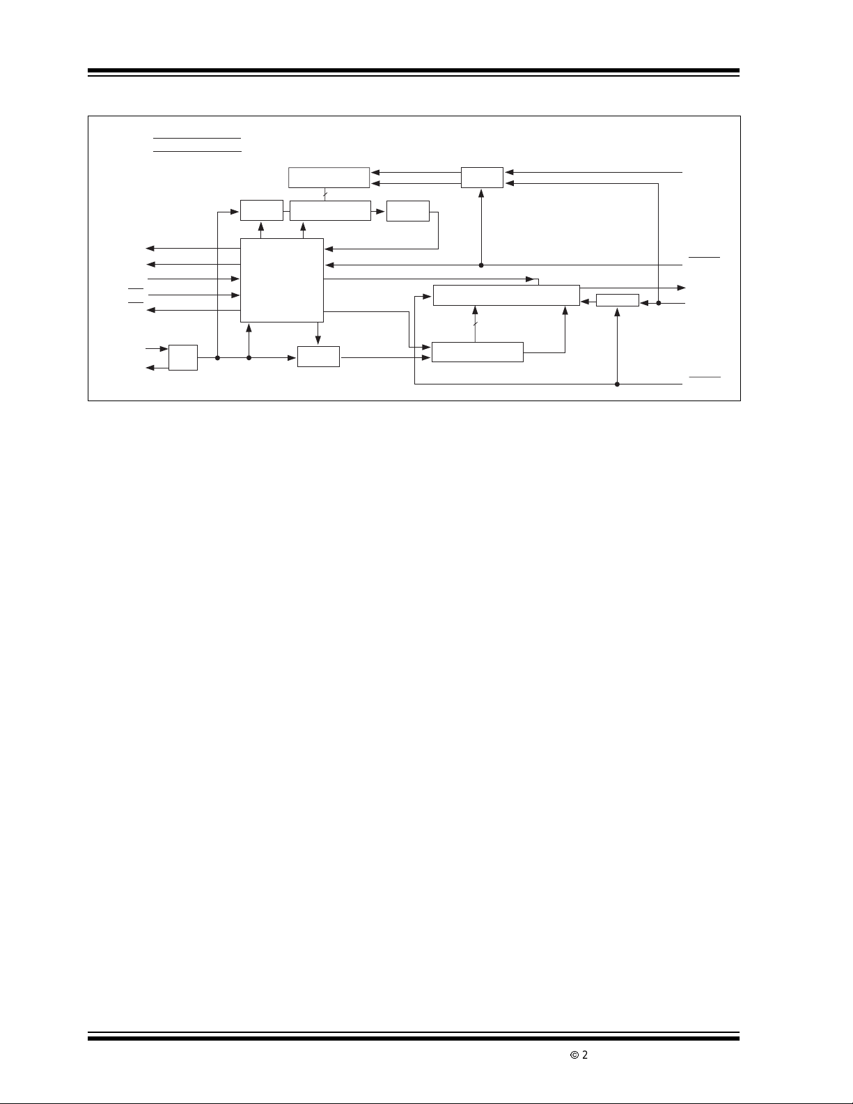
Functional Block Diagram
1
V
DD
2
GND
Gate
8-Bit Shift Reg.
8
8-Bit Counter
÷ 256
Gate
Pinout of 14-Pin
Package
11
D
IN
CMPTR
OSC
OSC
CE
DV
IN
OUT
Clear Count
Gate
Timeout
Force Auto Zero
Polarity Bit
18-Bit Shift Register
16
16-Bit Counter
Overrange
Bit
Gate
12
10
LOAD
9
D
OUT
D
CLK
8
READ
5
A
4
B
14
13
3
7
÷4
6
Logic Control
SYSCLK
DS21431B-page 2
2002 Microchip TechnologyInc.
TC520A
1.0 ELECTRICAL
CHARACTERISTICS
*Stresses above those listed under "Absolute Maximum Ratings"maycause permanentdamage to thedevice.These are
stress ratings only and functional operation of the device at
these or any other conditions above those indicated in the
Absolute Maximum Ratings*
DC Supply Voltage (VDD)....................................+6.0V
Input Voltage (All Inputs V
Operating Temperature Range (T
):.... - 0.3V to (VDD+0.3V)
IN
) .......... 0°C to 70°C
A
operation sections of the specifications is not implied. Exposure to Absolute Maximum R ating conditions for extended
periodsmay affectdevice reliability.
StorageTemperature Range..............-65°Cto +150°C
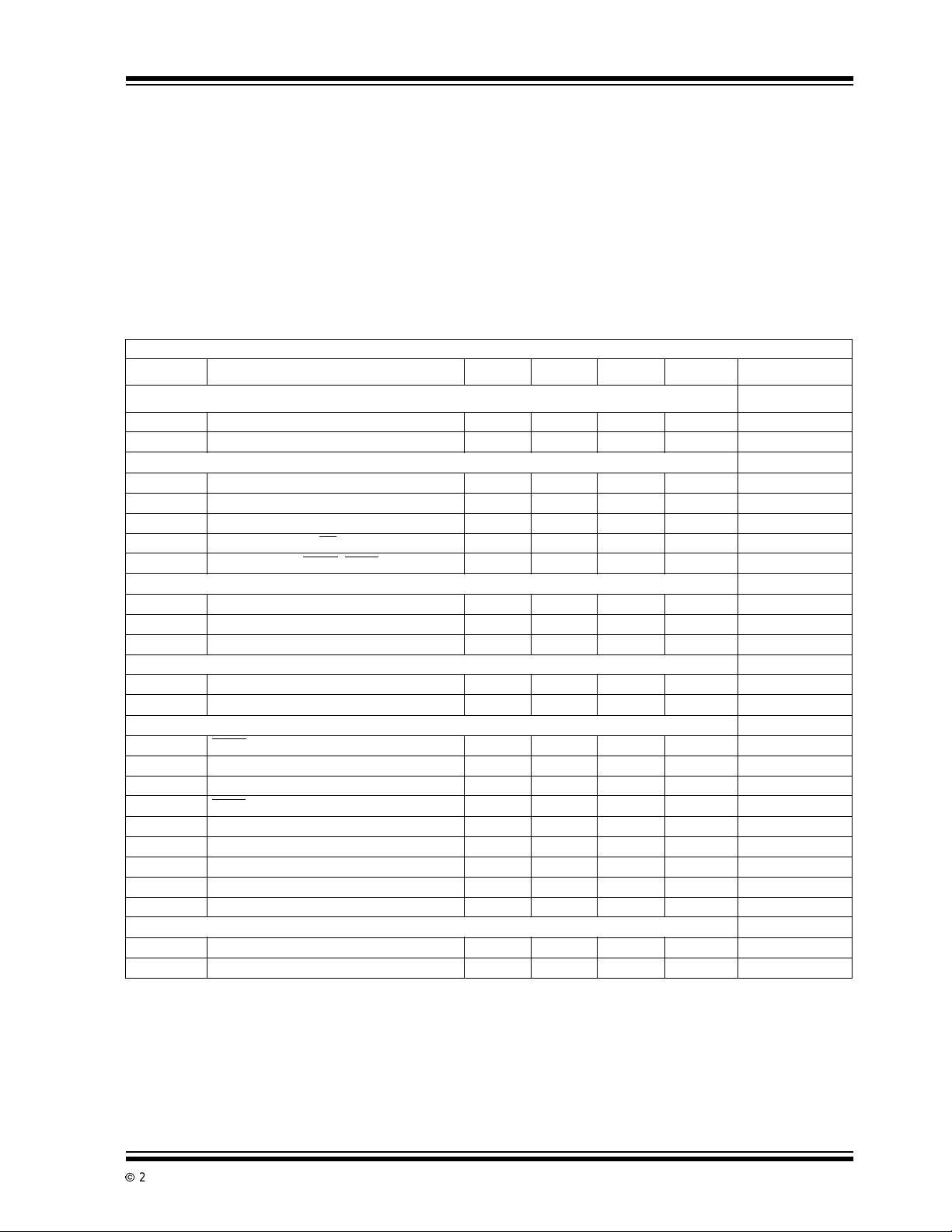
TC520A E LECTRI CAL SPECIFICATIONS
Electrical Characteristics: VDD=5V,F
Symbol Parameters Min Typ Max Unit Test Conditions
Supply
V
DD
I
DD
Operating Voltage Range 4.5 5 5.5 V
SupplyCurrent — 0.8 1.5 mA
Input Characteristics
V
V
I
IL
I
PD
I
PU
Output Characteristics (I
V
OL
V
OH
T
R,TF
Oscillator (OSC
F
XTL
F
OSC
Low InputVoltage — — 0.8 V
IL
HighInputVoltage 2.0 — — V
IH
InputLeakage Current — — 10 µA
Pull-down Current (CE)—5—µA
Pull-up Current (READ,LOAD)—5—µA
=250µA, VDD=5V)
OUT
Low Output Voltage — 0.2 0.3 V
High Output Voltage 3.5 4.3 — V
CL= 10pF, Rise/Fall Times — — 250 nsec
,OSC
IN
OUT
)
Crystal Frequency — 1.0 4.0 MHz
External Frequency(OSCIN)——6.0MHz
Timing Characteristics
READ Delay Time 250 — — nsec
Data Read Setup Time 1 — — µsec
D
CLK
to D
Delay 450 — — nsec
OUT
LOAD Setup Time 1 — — µsec
Data Load Setup Time 50 — — nsec
D
Pulse Width Low Time 150 — — nsec
CLK
D
Pulse Width High Time 150 — — nsec
CLK
Load Default Low Time 250 — — nsec
Load Default Setup Time 250 — — nsec
T
T
T
T
T
T
T
T
DRS
T
DLS
PWL
PWH
LDL
LDS
RD
RS
LS
Parameter
T
T
AZI
IntegratorZERO Time — 0.5 — msec
IZ
Auto zero (RESET) Time at Power-Up — 100 — msec
=1MHz,TA= +25°C, unless otherwise specified.
OSC
2002 Microchip TechnologyInc. DS21431B-page 3
TC520A
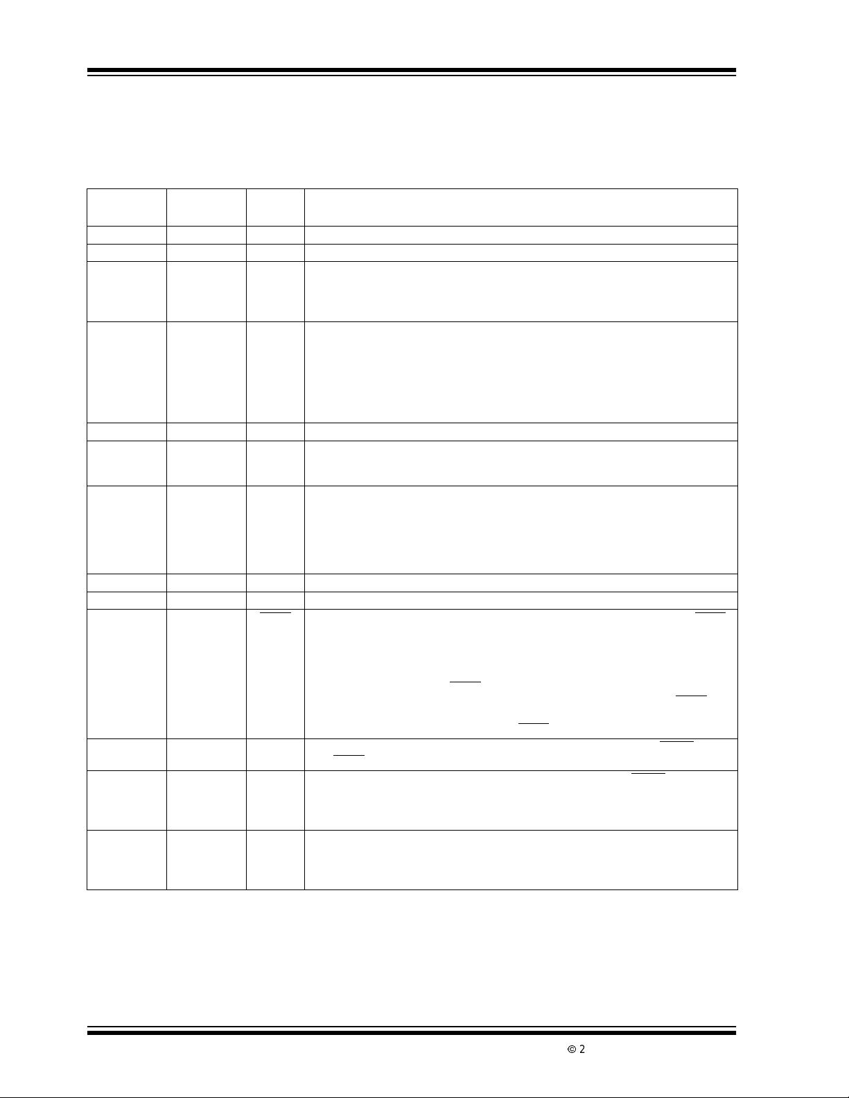
2.0 PIN DESCRIPTIONS
ThedescriptionsofthepinsarelistedinTable2-1
TABLE 2-1: PIN FUNCTION TABLE
Pin Number
14-Pin PDIP
11V
Pin Number
16-Pin SOIC
Symbol Description
Input. +5V ±10% power supply input with respect to DGND.
DD
2 2 DGND Input. Digital Ground.
3 3 CMPTR Input,active high or low (depending on polarity of the voltageinputtoA/D converter).
This pin connects directly to the zero crossing comparator output(CMPTR) of the
TC5XX A/D converter. A high-to-low state change on this pin causes the TC520A to
terminate the de-integrate phase of conversion.
4 4 B Output, active high. The A and B outputs of the TC520A connect directly to the A and B
inputs of the TC5XX A/D converter connected to the TC520A. The binary code on A, B
determines the conversion phase of the TC5XX A/D converter: (A, B) = 01 places the
TC5XX A/D converter into the Auto Zero phase; (A, B) =10 for Integrate phase (INT);
(A, B) =11 for De-integrate phase (DINI) and (A, B) = 00 for Integrator Zero phase (IZ).
Pleasesee the TC500/TC500A/TC510/TC514 family data sheetsfora complete
description of these phases of operation.
5 5 A Output, active high. See pin 4 description above.
66OSC
Input.Thispinconnects to one side of an AT-cut crystalhaving a effective series resis-
OUT
tance of 100Ω (typ.) and a parallel capacitance of 20pF (typ.). If an external frequency
sourceisused to clock the TC520A, this pin must be left floating.
77OSC
Input.Thispinconnects to the other side of the crystaldescribed in pin 6 above. The
IN
TC520Amayalsobe clocked from an external frequencysource connectedto thispin.
The externalfrequency source must be a pulse trainhaving a duty cycle of 30% (mini-
mum); rise and fall times of 15nsec and a min/max amplitude of 0 to V
frequency source is used, pin 6 must be left floating. A maximum operating frequency
.Ifanexternal
IH
of 4MHz (crystal) or 6MHz (external clock source) is permitted.
8 N/C No connection on 16 pin package version.
9 N/C No connection on 16 pin package version.
8 10 READ
Input, active low, level and negative edge triggered. A high-to-low transition on READ
loadsserial port output shiftregister with the most recent converted data.Datais
loaded such that the first bit transmitted from the TC520A to the processor is the
OVERRANGE bit (OVR), followed by the POLARITY bit (POL) (high = input positive;
low = input negative). This is followed by a 16-bit data word (MSB first). OVR is avail-
able at the D
data bit, if so desired. The D
held low. Otherwise, D
cycle is terminated at any time by bringing READ
911D
10 12 D
Output, logic level. Serialportoutput pin. This pin is enabled only when READ is low
OUT
(see READ
Input, positive and negative edge triggered. Serial port clock. With READ low, serial
CLK
dataisclocked into the TC520Aateachlow-to-high transitionof D
of the TC520A on each high-to-lowtransitionof D
as soon as READ is broughtlow. This bit may be used as the 17th
OUT
OUT
pin of the serial port is enabled only when READ is
OUT
remains in a high impedance state. A serial port read access
high.
pin description).
, and clockedout
.AmaximumserialportD
CLK
CLK
frequency of 3MHz is permitted.
11 13 D
Input, logic level. Serial port input pin. The TC5XX A/D converter integration time (T
IN
andAutoZero time (TAZ) values are determined by theLOADVALUEbyte clockedinto
this pin. This initialization must take place at power up and can be rewritten (or modified
and rewritten) at any time. The LOAD VALUE is clocked into D
MSB first.
IN
CLK
INT
)
DS21431B-page 4
2002 Microchip TechnologyInc.

TABLE 2-1: PIN FUNCTION TABLE (CONTINUED)
TC520A
Pin Number
14-Pin PDIP
12 14 LOAD Input, active low; level and edge triggered. The LOAD VALUE is clocked into the 8-bit
13 15 DV
14 16 CE
Pin Number
16-Pin SOIC
Symbol Description
shiftregister on board the TC520A while LOAD
transferred into the TC520A internal timebase counter (and becomes effective) when
LOAD
is returned high. If so desired, LOAD can be momentarily pulsedlow,eliminating
theneedtoclockaLOADVALUEintoD
clocked into the TC520A timebase counter selecting either a count of 65536
(D
= High), or count of 32768, (DIN=Low).
IN
Output,active low. DV is brought low any time the TC520A is in the AZ phase of conversion. This occurs when, either the TC520A initiates a normal AZ phase by setting A,
B, equal to 01, or when CE
andforcesanAZstate.DV
Input,active low,leveltriggered.Conversion willbe continuously performed as long as
CE
remains low. Pulling CE high causes the conversion process to be halted and
forcestheTC520A into the AZ mode for as long as CE
takenhighwhenever it is necessary to momentarilysuspend conversion (for example:
to change the address lines of an input multiplexer). CE
whentheTC520A entersanAZphase(i.e. when DV
excessively long integrator discharge times, which could result in erroneous conversion. This pin should be grounded if unused. It should be left floating if a 0.01µF
RESETcapacitor is connected to it (see Section 4.0, Typical Applications).
is pulled high, which overrides the normal A, B sequencing
is returnedhighwhentheTC520A exits AZ.
. In this case, the current stateof DINis
IN
is held low. The LOAD VALUE is then
remains high. CE should be
should be pulled high only
is low). This is necessary to avoid
2002 Microchip TechnologyInc. DS21431B-page 5
 Loading...