

TC4467
TC4468
TC4469
TC4467/8/9-6 10/21/96
© 2001 Microchip Technology Inc. DS21425A
LOGIC-INPUT CMOS QUAD DRIVERS
FEATURES
■ High Peak Output Current ............................... 1.2A
■ Wide Operating Range ............................ 4.5 to 18V
■ Symmetrical Rise and Fall Times................25nsec
■ Short, Equal Delay Times ............................75nsec
■ Latchproof! Withstands 500mA Inductive Kickback
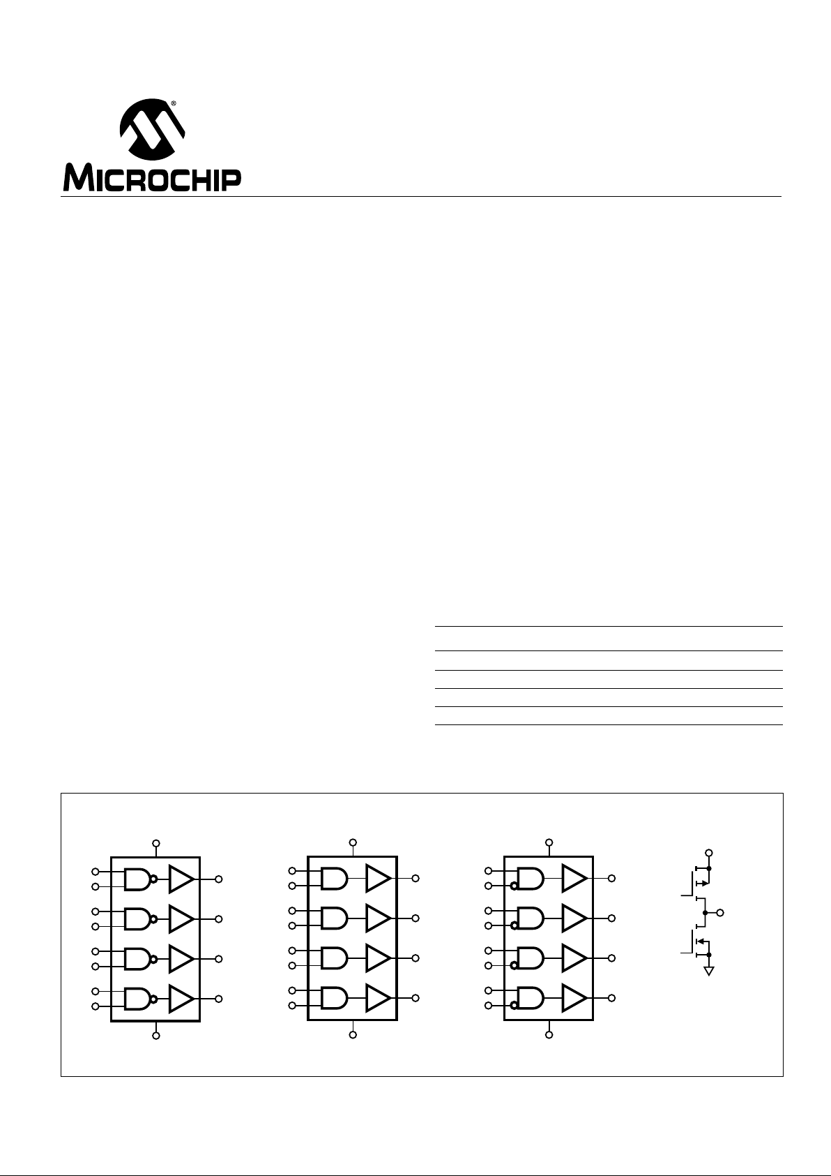
■ 3 Input Logic Choices
— AND / NAND / AND + Inv
■ 2kV ESD Protection on All Pins
APPLICATIONS
■ General-Purpose CMOS Logic Buffer
■ Driving All Four MOSFETs in an H-Bridge
■ Direct Small Motor Driver
■ Relay or Peripheral Drivers
■ CCD Driver
■ Pin-Switching Network Driver
ORDERING INFORMATION
Part No. Package Temp. Range
TC446xCOE 16-Pin SOIC (Wide) 0° to +70°C
TC446xCPD 14-Pin Plastic DIP 0° to +70°C
TC446xEJD 14-Pin CerDIP – 40° to +85°C
TC446xMJD 14-Pin CerDIP – 55° to +125°C
GENERAL DESCRIPTION
The TC446X family of four-output CMOS buffer/drivers
are an expansion from our earlier single- and dual-output
drivers. Each driver has been equipped with a two-input
logic gate for added flexibility.
The TC446X drivers can source up to 250 mA into loads
referenced to ground. Heavily loaded clock lines, coaxial
cables, and piezoelectric transducers can all be easily
driven with the 446X series drivers. The only limitation on
loading is that total power dissipation in the IC must be kept
within the power dissipation limits of the package.
The TC446X series will not latch under any conditions
within their power and voltage ratings. They are not subject
to damage when up to 5V of noise spiking (either polarity)
occurs on the ground line. They can accept up to half an amp
of inductive kickback current (either polarity) into their outputs without damage or logic upset. In addition, all terminals
are protected against ESD to at least 2000V.
*A digit must be added in the "x" position to define the device input
configuration: TC446x — 7 NAND
8 AND
9 AND with INV
LOGIC DIAGRAMS
TC4468
TC4467
OUTPUT
TC446X
V
DD
V
DD
14
7
1Y
13
1
2
1B
1A
2Y
12
3
4
2B
2A
3Y
11
5
6
3B
3A
4Y
10
8
9
4B
4A
GND
TC4469
V
DD
14
7
1Y
13
1
2
1B
1A
2Y
12
3
4
2B
2A
3Y
11
5
6
3B
3A
4Y
10
8
9
4B
4A
GND
V
DD
14
7
1Y
13
1
2
1B
1A
2Y
12
3
4
2B
2A
3Y
11
5
6
3B
3A
4Y
10
8
9
4B
4A
GND
2
LOGIC-INPUT CMOS QUAD DRIVERS
TC4467
TC4468
TC4469
TC4467/8/9-6 10/21/96
© 2001 Microchip Technology Inc. DS21425A
Package Thermal Resistance
14-Pin CerDIP R
θJ-A
......................................
100°C/W
R
θJ-C
.........................................
23°C/W
14-Pin Plastic DIP R
θJ-A
.........................................
80°C/W
R
θJ-C
.........................................
35°C/W
16-Pin Wide SOIC R
θJ-A
.........................................
95°C/W
R
θJ-C
.........................................
28°C/W
*Static-sensitive device. Unused devices must be stored in conductive
material. Protect devices from static discharge and static fields. Stresses
above those listed under Absolute Maximum Ratings may cause permanent damage to the device. These are stress ratings only and functional
operation of the device at these or any other conditions above those
indicated in the operational sections of the specifications is not implied.
Exposure to Absolute Maximum Rating Conditions for extended periods
may affect device reliability.
Symbol Parameter Test Conditions Min Typ Max Unit
Input
V
IH
Logic 1, High Input Voltage Note 3 2.4 — V
DD
V
V
IL
Logic 0, Low Input Voltage Note 3 0 — 0.8 V
I
IN
Input Current 0V ≤ VIN ≤ V
DD
– 1 — 1 µA
Output
V
OH
High Output Voltage I
LOAD
= 100µA (Note 1) VDD – 0.025 — — V
V
OL
Low Output Voltage I
LOAD
= 10mA (Note 1) — — 0.15 V
R
O
Output Resistance I
OUT
= 10mA, VDD = 18V — 10 15 Ω
I
PK
Peak Output Current — 1.2 — A
I
DC
Continuous Output Current Single Output — — 300 mA
Total Package 500
I Latch-Up Protection 4.5V ≤ VDD ≤ 16V 500 — — mA
Withstand Reverse Current
Switching Time
t
R
Rise Time Figure 1 — 15 25 nsec
t
F
Fall Time Figure 1 — 15 25 nsec
t
D1
Delay Time Figure 1 — 40 75 nsec
t
D2
Delay Time Figure 1 — 40 75 nsec
Power Supply
I
S
Power Supply Current — 1.5 4 mA
V
DD
Power Supply Voltage Note 2 4.5 — 18 V
ELECTRICAL CHARACTERISTICS:
Measured at TA = +25°C with 4.5V ≤ VDD ≤ 18V, unless otherwise specified.
TRUTH TABLE
Part No. TC4467 NAND TC4468 AND TC4469 AND/INV
INPUTS A H HL L HHLL HHLL
INPUTS B H LH L HLHL HLHL
OUTPUTS TC446X LHHH HLLL LHLL
H = High L = Low
ABSOLUTE MAXIMUM RATINGS*
Supply Voltage ......................................................... +20V
Input Voltage ......................... (GND – 5V) to (VDD + 0.3V)
Maximum Chip Temperature
Operating........................................................+150°C
Storage ............................................. – 65° to +150°C
Maximum Lead Temperature
(Soldering, 10 sec) .........................................+300°C
Operating Ambient Temperature Range
C Device .................................................. 0° to +70°C
E Device ............................................. – 40° to +85°C
M Device........................................... – 55° to +125°C
Package Power Dissipation (T
A
≤ 70°C)
14-Pin CerDIP ................................................840mW
14-Pin Plastic DIP...........................................800mW
16-Pin Wide SOIC ..........................................760mW
3
LOGIC-INPUT CMOS QUAD DRIVERS
TC4467
TC4468
TC4469
TC4467/8/9-6 10/21/96
© 2001 Microchip Technology Inc. DS21425A
Symbol Parameter Test Conditions Min Typ Max Unit
Input
V
IH
Logic 1, High Input Voltage (Note 3) 2.4 — — V
V
IL
Logic 0, Low Input Voltage (Note 3) — — 0.8 V
I
IN
Input Current 0V ≤ VIN ≤ V
DD
– 10 — 10 µA
Output
V
OH
High Output Voltage I
LOAD
= 100µA (Note 1) V
DD
– 0.025 — — V
V
OL
Low Output Voltage I
LOAD
= 10mA (Note 1) — — 0.30 V
R
O
Output Resistance I
OUT
= 10mA, VDD = 18V — 20 30 Ω
I
PK
Peak Output Current — 1.2 — A
I Latch-Up Protection 4.5V ≤ VDD ≤ 16V 500 — — mA
Withstand Reverse Current
Switching Time
t
R
Rise Time Figure 1 — — 50 nsec
t
F
Fall Time Figure 1 — — 50 nsec
t
D1
Delay Time Figure 1 — — 100 nsec
t
D2
Delay Time Figure 1 — — 100 nsec
Power Supply
I
S
Power Supply Current — — 8 mA
I
S
Power Supply Voltage Note 2 4.5 — 18 V
ELECTRICAL CHARACTERISTICS: Measured throughout operating temperature range with 4.5V ≤ V
Dd
≤ 18V,
unless otherwise specified.
NOTES: 1. Totem-pole outputs should not be paralleled because the propagation delay differences from one to the other could cause one driver to drive
high a few nanoseconds before another. The resulting current spike, although short, may decrease the life of the device.
2. When driving all four outputs simultaneously in the same direction, VDD shall be limited to 16V. This reduces the chance that internal
dv/dt will cause high-power dissipation in the device.
3. The input threshold has about 50mV of hysteresis centered at approximately 1.5V. Slow moving inputs will force the device to
dissipate high peak currents as the input transitions through this band. Input rise times should be kept below 5µsec to avoid high internal peak
currents during input transitions. Static input levels should also be maintained above the maximum or below the minimum input levels
specified in the "Electrical Characteristics" to avoid increased power dissipation in the device.
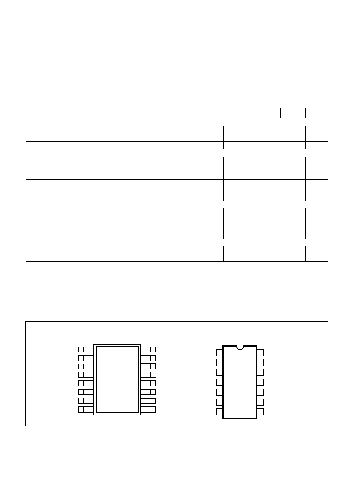
PIN CONFIGURATIONS
1
2
3
4
5
6
7
14
13
12
11
10
9
8
1A
1B
2A
2B
3A
3B
GND
V
1Y
2Y
3Y
4Y
4B
4A
DD
1
2
3
4
5
6
7
8
16
13
12
11
10
9
1A
1B
2A
2B
3A
3B
GND
GND
V
1Y
2Y
3Y
4Y
4B
4A
DD
V
DD
15
14
TC4467/8/9
TC4467/8/9
16-Pin SOIC (Wide)
14-Pin Plastic DIP/CerDIP

4
LOGIC-INPUT CMOS QUAD DRIVERS
TC4467
TC4468
TC4469
TC4467/8/9-6 10/21/96
© 2001 Microchip Technology Inc. DS21425A
Three components make up total package power
dissipation:
(1) Load-caused dissipation (PL)
(2) Quiescent power (PQ)
(3) Transition power (PT).
A capacitive-load-caused dissipation (driving MOSFET
gates), is a direct function of frequency, capacitive load, and
supply voltage. The power dissipation is:
PL = f C V
S
2
,
where: f = Switching frequency
C = Capacitive load
VS = Supply voltage.
A resistive-load-caused dissipation for ground-referenced loads is a function of duty cycle, load current, and
load voltage. The power dissipation is:
PL = D (VS – VL) IL,
where: D = Duty cycle
VS = Supply voltage
VL = Load voltage
IL = Load current.
A resistive-load-caused dissipation for supply-referenced loads is a function of duty cycle, load current, and
output voltage. The power dissipation is:
PL = D VO IL,
where: f = Switching frequency
VO = Device output voltage
IL = Load current.
Quiescent power dissipation depends on input signal
duty cycle. Logic HIGH outputs result in a lower power
dissipation mode, with only 0.6 mA total current drain (all
devices driven). Logic LOW outputs raise the current to 4 mA
maximum. The quiescent power dissipation is:
PQ = VS (D(IH) + (1–D)IL),
where: IH = Quiescent current with all outputs LOW
(4 mA max)
IL = Quiescent current with all outputs HIGH
(0.6mA max)
D = Duty cycle
VS =Supply voltage.
Supply Bypassing
Large currents are required to charge and discharge
large capacitive loads quickly. For example, charging a
1000pF load to 18V in 25nsec requires 0.72A from the
device's power supply.
To guarantee low supply impedance over a wide frequency range, a 1µF film capacitor in parallel with one or two
low-inductance 0.1µF ceramic disk capacitors with short
lead lengths (<0.5 in.) normally provide adequate bypassing.
Grounding
The TC4467 and TC4469 contain inverting drivers.
Potential drops developed in common ground impedances
from input to output will appear as negative feedback and
degrade switching speed characteristics. Instead, individual
ground returns for input and output circuits, or a ground
plane, should be used.
Input Stage
The input voltage level changes the no-load or quiescent supply current. The N-channel MOSFET input stage
transistor drives a 2.5mA current source load. With logic "0"
outputs, maximum quiescent supply current is 4mA. Logic
"1" output level signals reduce quiescent current to 1.4mA
maximum. Unused driver inputs must be connected to V
DD
or VSS. Minimum power dissipation occurs for logic "1"
outputs.
The drivers are designed with 50mV of hysteresis. This
provides clean transitions and minimizes output stage current spiking when changing states. Input voltage thresholds
are approximately 1.5V, making any voltage greater than
1.5V up to V
DD
a logic 1 input . Input current is less than 1 µA
over this range.
Power Dissipation
The supply current versus frequency and supply current
versus capacitive load characteristic curves will aid in determining power dissipation calculations. TelCom Semiconductor's CMOS drivers have greatly reduced quiescent DC
power consumption.
Input signal duty cycle, power supply voltage and load
type, influence package power dissipation. Given power
dissipation and package thermal resistance, the maximum
ambient operating temperature is easily calculated. The
14-pin plastic package junction-to-ambient thermal resistance is 83.3°C/W. At +70°C, the package is rated at
800mW maximum dissipation. Maximum allowable chip
temperature is +150°C.

5
LOGIC-INPUT CMOS QUAD DRIVERS
TC4467
TC4468
TC4469
TC4467/8/9-6 10/21/96
© 2001 Microchip Technology Inc. DS21425A
Maximum operating temperature:
TJ – θJA (PD) = 141°C,
where: TJ = Maximum allowable junction temperature
(+150°C)
θJA = Junction-to-ambient thermal resistance
(83.3°C/W) 14-pin plastic package.
NOTE: Ambient operating temperature should not exceed +85°C for
"EJD" device or +125°C for "MJD" device.
Figure 1. Switching Time Test Circuit
V
OUT
1B
1A
2B
2A
3B
3A
4B
4A
1 µF FILM 0.1 µF CERAMIC
V
DD
470 pF
90%
10%
10%
10%
t
D1
t
R
t
D2
t
F
90%
+5V
INPUT
(A, B)
V
DD
OUTPUT
0V
0V
90%
1
2
3
4
5
6
8
9
7
10
11
12
13
14
Input: 100 kHz, square wave,
t
RISE
= t
FALL
≤ 10nsec
Transition power dissipation arises in the
complementary configuration (TC446X) because the
output stage N-channel and P-channel MOS transistors
are ON simultaneously for a very short period when the
output changes. The transition power dissipation is
approximately:
PT = f VS (10 10–9).
Package power dissipation is the sum of load, quiescent and transition power dissipations. An example shows
the relative magnitude for each term:
C = 1000pF capacitive load
V
S
= 15V
D = 50%
f = 200kHz
PD= Package Power Dissipation = PL + PQ + P
T
= 45mW + 35 mW + 30 mW = 110mW.

6
LOGIC-INPUT CMOS QUAD DRIVERS
TC4467
TC4468
TC4469
TC4467/8/9-6 10/21/96
© 2001 Microchip Technology Inc. DS21425A
TYPICAL CHARACTERISTICS
140
120
100
80
60
40
20
0
3 5 7 9 11 13 15 17
19
V (V)
SUPPLY
2200 pF
1600 pF
1000 pF
470 pF
100 pF
t (nsec)
(RISE)
Rise Time vs. Supply Voltage
140
120
100
80
60
40
20
0
3 5 7 9 11 13 15 17
19
V (V)
SUPPLY
t (nsec)
(FALL)
100 pF
470 pF
1000 pF
1500 pF
2200 pF
Fall Time vs. Supply Voltage
140
120
100
80
60
40
20
0
100 1000
10,000
C (pF)
LOAD
t (nsec)
(RISE)
10V
15V
5V
Rise Time vs. Capacitive Load
140
120
100
80
60
40
20
0
100 1000
10,000
C (pF)
LOAD
t (nsec)
(FALL)
5V
10V
15V
Fall Time vs. Capacitive Load
0
–50
TEMPERATURE (°C)
TIME (nsec)
5
10
15
20
25
–25 0 25 50 75 100 125
t
V = 17.5V
C = 470 pF
t
SUPPLY
LOAD
(FALL)
(RISE)
Rise/Fall Times vs. Temperature
0
4
DELAY TIME (nsec)
20
40
60
80
812141618610
V (V)
SUPPLY
t
C = 470 pF
LOAD
D1
Propagation Delay Time vs. Supply Voltage
t
D2

7
LOGIC-INPUT CMOS QUAD DRIVERS
TC4467
TC4468
TC4469
TC4467/8/9-6 10/21/96
© 2001 Microchip Technology Inc. DS21425A
TYPICAL CHARACTERISTICS (Cont.)
140
120
100
80
60
40
20
0
19
10
V(V)
DRIVE
DELAY TIME (nsec)
2345678
INPUT FALLING
t
t
INPUT RISING
V = 12V
DD
D1
D2
Input Amplitude vs. Delay Times
70
20
100
120
TEMPERATURE (°C)
DELAY TIME (nsec)
–40 –20 0 20 40 60 80
30
40
50
60
V = 17.5V
C = 470 pF
V = 0, 5V
DD
LOAD
IN
t
t
D1
D2
Propagation Delay Times vs. Temperature
–60
0
4
0.5
1.0
1.5
2.0
2.5
6 8 10 12 14 16 18
V
SUPPLY
(V)
I (mA)
QUIESCENT
Quiescent Supply Current vs. Supply Voltage
3.5
0
100
120
T (°C)
–40 –20 0 20 40 60 80
3.0
2.5
2.0
1.5
1.0
0.5
I (mA)
QUIESCENT
V = 17.5V
DD
OUTPUTS HIGH
OUTPUTS LOW
JUNCTION
Quiescent Supply Current vs. Temperature
–60
0
4 6 8 1012141618
V
SUPPLY
(V)
5
10
15
20
25
30
35
T = +150°C
T = +25°C
R ( )Ω
DS(ON)
J
High-State Output Resistance
J
0
4 6 8 10 12 14 16 18
5
10
15
20
25
30
35
T = +150°C
T = +25°C
J
J
Low-State Output Resistance
V
SUPPLY
(V)
R ( )Ω
DS(ON)
OUTPUTS = 1
OUTPUTS = 0

8
LOGIC-INPUT CMOS QUAD DRIVERS
TC4467
TC4468
TC4469
TC4467/8/9-6 10/21/96
© 2001 Microchip Technology Inc. DS21425A
SUPPLY CURRENT CHARACTERISTICS (Load on Single Output Only)
60
0
100 1000
10,000
C (pF)
LOAD
50
40
30
20
10
2 MHz
1 MHz
500 kHz
200 kHz
20 kHz
I (mA)
SUPPLY
V = 18V
DD
Supply Current vs. Capacitive Load
60
0
100 1000
FREQUENCY (kHz)
50
40
30
20
10
I (mA)
SUPPLY
V = 18V
DD
2200 pF
1000 pF
100 pF
10
Supply Current vs. Frequency
10,000
60
0
100 1000
10,000
50
40
30
20
10
C (pF)
LOAD
I (mA)
SUPPLY
V = 12V
DD
2 MHz
1 MHz
500 kHz
200 kHz
20 kHz
Supply Current vs. Capacitive Load
60
0
10 100
FREQUENCY (kHz)
50
40
30
20
10
1000
I (mA)
SUPPLY
2200 pF
1000 pF
100 pF
V = 12V
DD
Supply Current vs. Frequency
10,000
60
50
40
30
20
10
0
100 1000
10,000
C (pF)
LOAD
I (mA)
SUPPLY
1 MHz
500 kHz
200 kHz
20 kHz
2 MHz
V = 6V
DD
Supply Current vs. Capacitive Load
60
0
10 1000
100
FREQUENCY (kHz)
50
40
30
20
10
I (mA)
SUPPLY
V = 6V
DD
2200 pF
1000 pF
100 pF
Supply Current vs. Frequency
10,000

9
LOGIC-INPUT CMOS QUAD DRIVERS
TC4467
TC4468
TC4469
TC4467/8/9-6 10/21/96
© 2001 Microchip Technology Inc. DS21425A
TYPICAL APPLICATIONS
4.7 kΩ
TC4469
48-Volt, 3-Phase Brushless Output Stage
1
2
3
4
5
6
8
9
1B
2A
2B
3A
3B
4A
4B
1Y
2Y
3Y
4Y
GND
U1
13
12
11
10
TC4469
1
2
3
4
5
6
8
9
1A
1B
2A
2B
3A
3B
4A
4B
1Y
2Y
3Y
4Y
13
12
11
10
48V
14
7
15V
14
7
GND
V
DD
R4
3.3
kΩ
D2
D3
D4
R1
3.3
kΩ
5W
R9
R10
R11
Q1
Q2
Q3
2N5550
2N5550
2N5550
1A
A+
B+
C+
A–
B–
C–
C1
1 µF
D1
1N4744
15V
R2
3.3
kΩ
R3
3.3
kΩ
MOTOR MOTOR MOTOR
4.7 kΩ
4.7 k
Ω
U2
V
DD
PHASE A
PHASE B
PHASE C
(FLOAT AT 33V)
R7
R6
R5
+12V
14
7
1
2
Stepper Motor Drive
TC4469
13
3
4
12
5
6
11
8
9
10
A
B
+5V TO +15V
14
Quad Driver for H-Bridge Motor Control
TC4469
DIRECTION
PWM SPEED
18V
FWD
13
12
11
10
7
9
8
6
5
4
3
2
1
REV
MOTOR
MOTORM
RED
GRAY
YEL
BLK
AIRPAX
#M82102-P2
7.5°/STEP

10
LOGIC-INPUT CMOS QUAD DRIVERS
TC4467
TC4468
TC4469
TC4467/8/9-6 10/21/96
© 2001 Microchip Technology Inc. DS21425A
PACKAGE DIMENSIONS
Dimensions: inches (mm)
.260 (6.60)
.240 (6.10)
.770 (19.56)
.745 (18.92)
.310 (7.87)
.290 (7.37)
.040 (1.02)
.020 (0.51)
.070 (1.78)
.045 (1.14)
.022 (0.56)
.015 (0.38)
.110 (2.79)
.090 (2.29)
.200 (5.08)
.140 (3.56)
.150 (3.81)
.115 (2.92)
PIN 1
.015 (0.38)
.008 (0.20)
3° MIN.
.400 (10.16)
.310 (7.87)
14-Pin Plastic DIP
14-Pin CerDIP
.780 (19.81)
.740 (18.80)
.300 (7.62)
.230 (5.84)
.200 (5.08)
.160 (4.06)
.200 (5.08)
.125 (3.18)
.110 (2.79)
.090 (2.29)
.065 (1.65)
.045 (1.14)
.020 (0.51)
.016 (0.41)
.040 (1.02)
.020 (0.51)
.098 (2.49) MAX. .030 (0.76) MIN.
.400 (10.16)
.320 (8.13)
.015 (0.38)
.008 (0.20)
3° MIN.
PIN 1
.320 (8.13)
.290 (7.37)
.150 (3.81)
MIN.

11
LOGIC-INPUT CMOS QUAD DRIVERS
TC4467
TC4468
TC4469
TC4467/8/9-6 10/21/96
© 2001 Microchip Technology Inc. DS21425A
PACKAGE DIMENSIONS (Cont.)
16-Pin SOIC (Wide)
Dimensions: inches (mm)
8°
MAX.
PIN 1
.299 (7.59)
.291 (7.40)
.413 (10.49)
.398 (10.10)
.019 (0.48)
.014 (0.36)
.012 (0.30)
.004 (0.10)
.104 (2.64)
.097 (2.46)
.013 (0.33)
.009 (0.23)
.050 (1.27)
.016 (0.40)
.419 (10.65)
.398 (10.10)
.050 (1.27) TYP.

12
LOGIC-INPUT CMOS QUAD DRIVERS
TC4467
TC4468
TC4469
TC4467/8/9-6 10/21/96
© 2001 Microchip Technology Inc. DS21425A
Information contained in this publication regarding device applications and the like is intended through suggestion only and may be superseded by
updates. It is your re sponsib ility to en sure t hat your appl ication m eets with y our sp ecifications . No re presen tation or warra nty is given and no liability is
assumed by Microchip Technology Incorporated with re spect t o the accur acy or use of such infor mation, or infrin gement of paten ts or o th er i nte lle ct ua l
property rights arising from such use or otherwise. Use of Microchipís products as critical components in life support systems is not authorized except with
express written approval by Microchip. No licenses are conveyed, implicitly or otherwise, except as maybe explicitly expressed herein, under any intellectual property rights. The Micro chip logo and name are registered trad emarks of Microchip Technology Inc. in the U.S.A. and othe r countries. All rights
reserved. All other trademarks mentioned herein are the property of their respective companies.
All rights reserved. © 2001 Microchip Technology Incorporated. Printed in the USA. 1/01 Printed on recycled paper.
AMERICAS
Corporate Office
2355 West Chandler Blvd.
Chandler, AZ 85224-6199
Tel: 480-792-7200 Fax: 480-792-7277
Technical Support: 480-792-7627
Web Address: http://www.microchip.com
Rocky Mountain
2355 West Chandler Blvd.
Chandler, AZ 85224-6199
Tel: 480-792-7966 Fax: 480-792-7456
Atlanta
500 Sugar Mill Road, Suite 200B
Atlanta, GA 30350
Tel: 770-640-0034 Fax: 770-640-03 07
Austin
Analog Product Sales
8303 MoPac Expressway North
Suite A-201
Austin, TX 78759
Tel: 512-345-2030 Fax: 512-345-60 85
Boston
2 Lan Drive, Suite 120
Westford, MA 01886
Tel: 978-692-3848 Fax: 978-692-38 21
Boston
Analog Product Sales
Unit A-8-1 Millbrook Tarry Condominium
97 Lowell Road
Concord, MA 01742
Tel: 978-371-6400 Fax: 978-371-00 50
Chicago
333 Pierce Road, Suite 180
Itasca, IL 60143
Tel: 630-285-0071 Fax: 630-285 -00 75
Dallas
4570 Westgrove Drive, Suite 160
Addison, TX 75001
Tel: 972-818-7423 Fax: 972-818-29 24
Dayton
Two Prestige Place, Suite 130
Miamisburg, OH 45342
Tel: 937-291-1654 Fax: 937-291-91 75
Detroit
Tri-Atria Office Building
32255 Northwestern Highway, Suite 190
Farmington Hills, MI 48334
Tel: 248-538-2250 Fax: 248-538 -22 60
Los Angeles
18201 Von Karman, Suite 1090
Irvine, CA 92612
Tel: 949-263-1888 Fax: 949-263-13 38
Mountain View
Analog Product Sales
1300 Terra Bella Avenue
Mountain View, CA 94043-1836
Tel: 650-968-9241 Fax: 650-967-15 90
New York
150 Motor Parkway, Suite 202
Hauppauge, NY 11788
Tel: 631-273-5305 Fax: 631-273-5335
San Jose
Microchip Technology Inc.
2107 North First Street, Suite 590
San Jose, CA 95131
Tel: 408-436-7950 Fax: 408-436-7955
Toronto
6285 Northam Drive, Suite 108
Mississauga, Ontari o L4V 1X5, Ca nada
Tel: 905-673-0699 Fax: 905-673-6509
ASIA/PACIFIC
China - Beijing
Microchip Technology Beijing Office
Unit 915
New China Hong Kong Manhattan Bldg.
No. 6 Chaoyangmen Beidajie
Beijing, 100027, No. China
Tel: 86-10-85282100 Fax: 86-10-85282104
China - Shanghai
Microchip Technology Shanghai Office
Room 701, Bldg. B
Far East International Plaza
No. 317 Xian Xia Road
Shanghai, 200051
Tel: 86-21-6275-5700 Fax: 86-21-6275-5060
Hong Kong
Microchip Asia Pacific
RM 2101, Tower 2, Metroplaza
223 Hing Fong Road
Kwai Fong, N.T., Hong Kong
Tel: 852-2401-1200 Fax: 852-2401-3431
India
Microchip Technology Inc.
India Liaison Office
Divyasree Chambers
1 Floor, Wing A (A3/A4)
No. 11, OíShaugnessey Road
Bangalore, 560 025, India
Tel: 91-80-2290061 Fax: 91-80-2290062
Japan
Microchip Technology Intl. Inc.
Benex S-1 6F
3-18-20, Shinyokohama
Kohoku-Ku, Yokohama-shi
Kanagawa, 222-0033, Japan
Tel: 81-45-471- 6166 Fax: 81-45-471-6122
Korea
Microchip Technology Korea
168-1, Youngbo Bldg. 3 Floor
Samsung-Dong, Kangnam-Ku
Seoul, Korea
Tel: 82-2-554-7200 Fax: 82-2-558-5934
ASIA/PACIFIC
(continued)
Singapore
Microchip Technology Singapore Pte Ltd.
200 Middle Road
#07-02 Prime Centre
Singapore, 188980
Tel: 65-334-8870 Fax: 65-334-8850
Taiwan
Microchip Technology Taiwan
11F-3, No. 207
Tung Hua North Road
Taipei, 105, Taiwan
Tel: 886-2-2717-7175 Fax: 886-2-2545-0139
EUROPE
Australia
Microchip Technology Australia Pty Ltd
Suite 22, 41 Rawson Street
Epping 2121, NSW
Australia
Tel: 61-2-9868-6733 Fax: 61-2-9868-6755
Denmark
Microchip Technology Denmark ApS
Regus Business Centre
Lautrup hoj 1-3
Ballerup DK -2750 Denmark
Tel: 45 4420 9895 Fax: 45 4420 9910
France
Arizona Microchip Technology SARL
Parc díActivite du Moulin de Massy
43 Rue du Saule Trapu
Batiment A - ler Etage
91300 Massy, France
Tel: 33-1-69-53-63-20 Fax: 33-1-69-30-90-79
Germany
Arizona Microchip Technology GmbH
Gustav-Heinemann Ring 125
D-81739 Munich, Germany
Tel: 49-89-627-144 0 Fax: 49-89-627-144-44
Germany
Analog Product Sales
Lochhamer Strasse 13
D-82152 Martinsried, Germany
Tel: 49-89-895650-0 Fax: 49-89-895650-22
Italy
Arizona Microchip Technology SRL
Centro Direzionale Colleoni
Palazzo Taurus 1 V. Le Colleoni 1
20041 Agrate Brianza
Milan, Italy
Tel: 39-039-65791-1 Fax: 39-039-6899883
United Kingdom
Arizona Microchip Technology Ltd.
505 Eskdale Road
Winnersh Triangle
Wokingham
Berkshire, England RG41 5TU
Tel: 44 118 921 5869 Fax: 44-118 921-5820
01/09/01
W
ORLDWIDE SALES AND SERVICE
 Loading...