

M
GND
300mV
2
g
g
g
t
t
e
t
9A High-Speed MOSFET Drivers
TC4421/TC4422
Features
• Tough CMOS Construction
• High Peak Output Current: 9A
• High Continuous Output Current: 2A Max
• Fast Rise and Fall Times:
- 30nsec with 4,700pF Load
- 180nsec with 47,000pF Load
• Short Internal Delays: 30nsec Typ.
• Low Output Impedance: 1.4Ω Typ.
Applications
• Line Drivers for Extra-Heavily-Loaded Lines
• Pulse Generators
• Driving the Largest MOSFETs and IGBTs
• Local Power ON/OFF Switch
• Motor and Solenoid Driver
Device Selection Table
Part Number Package Temp. Range
TC4421CAT 5-Pin TO-220 0°C to +70°C
TC4421CPA 8-Pin PDIP 0°C to +70°C
TC4421EPA 8-Pin PDIP -40°C to +85°C
TC4421MJA 8-Pin CERDIP -55°C to +125°C
TC4422CAT 5-Pin TO-220 0°C to +70°C
TC4422CPA 8-Pin PDIP 0°C to +70°C
TC4422EPA 8-Pin PDIP -40°C to +85°C
TC4422MJA 8-Pin CERDIP -55°C to +125°C
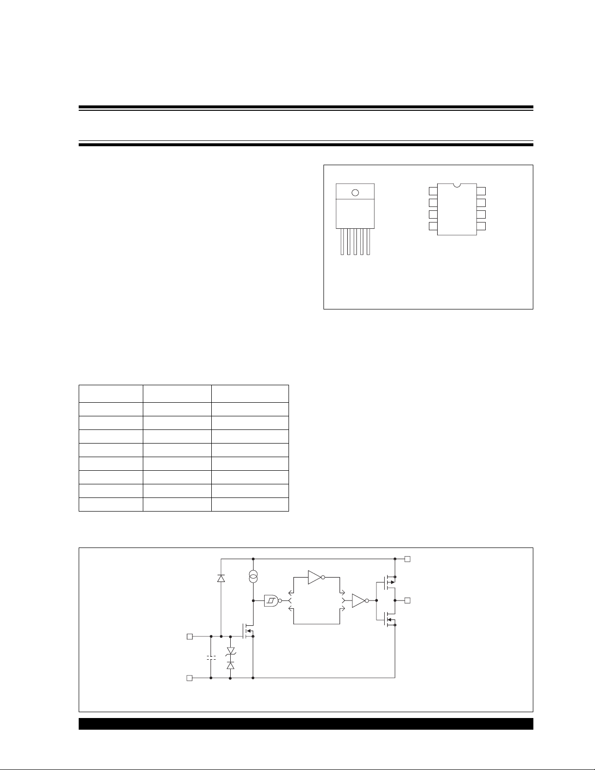
Package Type
8-Pin PDIP/CERDIPTO-220-5
1
V
DD
INPUT
2
TC4421
TC4421
TC4422
Tab is
Common
to V
DD
V
GND
GND
INPUT
OUTPUT
NC = No connection
NOTE: Duplicate pins must both be connected for proper operation.
GND
DD
TC4422
NC
3
45
V
DD
78OUTPUT
6
OUTPUT
GND
General Description
The TC4421/TC4422 are high current buffer/drivers
capable of driving large MOSFETs and IGBTs.
They are essentially immune to any form of upset
except direct overvoltage or over-dissipation – they
cannot be latched under any conditions within their
power and voltage ratings; they are not subject to
damage or imprope r operation when up t o 5V of ground
bounce is present on their ground terminals; they can
accept, without either damage or logic upset, more
than 1A inductive curre nt of ei ther polari ty bein g force d
back into their output s. In addition, a ll terminals are fu lly
protected against up to 4kV of electrostatic discharge.
The TC4421/TC4422 inputs may be driven directly
from either TTL or CMOS (3V to 18V). In addition,
300mV of hysteresis is built into the input, providing
noise immunity and allowing the device to be driven
from slowly rising or falling waveforms.
Functional Block Diagram
Invertin
Outpu
Inpu
Effectiv
Inpu
C = 25pF
2002 Microchip Technology Inc. DS21420B-page 1
Noninvertin
TC4421/TC442
Inverting/Noninvertin
TC4421/TC4422
1.0 ELECTRICAL
CHARACTERISTICS
Absolute Maximum Ratings*
Supply Voltage .....................................................+20V
Input Voltage ....................(VDD + 0.3V) to (GND – 5V)
Input Current (V
Package Power Dissipation (T
PDIP.........................................................730mW
CERDIP....................................................800mW
5-Pin TO-220................................................1.6W
Package Power Dissipation (T
5-Pin TO-220 (With Heatsink)....................12.5W
Derating Factors (To Ambient )
PDIP........................................................8mW/°C
CERDIP................................................6.4mW/°C
5-Pin TO-220.........................................12mW/°C
Thermal Impedances (To Case)
5-Pin TO-220 R
Operating Temperature Range (Ambient)
C Version.........................................0°C to +70°C
E Version......................................-40°C to +85°C
M Version ...................................-55°C to +125°C
Storage Temperature Range..............-65°C to +150°C
> VDD)....................................50mA
IN
≤ 70°C)
A
≤ 25°C)
A
..................................10°C/W
θJ-C
*Stresses above those listed under "Absolute Maximum
Ratings" may cause permanent damage to the device. These
are stress ratings only and functional operation of the device
at these or any other conditions above those indicated in the
operation sections of the specifications is not implied.
Exposure to Absolute Maximum Rating conditions for
extended periods may affect device reliability.
TC4421/TC4422 ELECTRICAL SPEC IFICA TI ON S
Electrical Characteristics: TA = +25°C, with 4.5V ≤ V
Symbol Parameter Min Typ Max Units Test Conditions
Input
V
IH
V
IL
I
IN
Output
V
OH
V
OL
R
O
R
O
I
PK
I
DC
I
REV
Switching Time (Note 1)
t
R
t
F
t
D1
t
D2
Note 1: Switching times ensured by design.
Logic 1, High Input Voltage 2.4 1.8 — V
Logic 0, Low Input Voltage — 1.3 0.8 V
Input Current -10 — 10 µA0V ≤ V
High Output Voltage VDD – 0.025 ——V Figure 3-1
Low Output Voltage ——0.025 V Figure 3-1
Output Resistance, High — 1.4 — Ω I
Output Resistance, Low — 0.9 1.7 Ω I
Peak Output Current — 9 — AVDD = 18V
Continuous Output Current 2 —— A 10V ≤ VDD ≤ 18V, TA = +25°C
Latch-Up Protection
Withstand Reverse Current
Rise Time — 60 75 nsec Figure 3-1, CL = 10,000pF
Fall Time — 60 75 nsec Figure 3-1, CL = 10,000pF
Delay Time — 30 60 nsec Figure 3-1
Delay Time — 33 60 nsec Figure 3-1
≤ 18V, unless otherwise noted.
DD
≤ V
IN
DD
= 10mA, VDD = 18V
OUT
= 10mA, VDD = 18V
OUT
(TC4421/TC4422 CAT only)
— >1.5 — A Duty cycle ≤ 2%, t ≤ 300µsec
DS21420B-page 2 2002 Microchip Technology Inc.

TC4421/TC4422
TC4421/TC4422 ELECTRICAL SPECIFICATIONS (CONTINUED)
Electrical Characteristics: TA = +25°C, with 4.5V ≤ V
Symbol Parameter Min Typ Max Units Test Conditions
Power Supply
I
S
V
DD
Power Supply Current —
Operating Input Voltage 4.5 — 18 V
Electrical Characteristics: Over operating temperature range with 4.5V
Symbol Parameter Min Typ Max Units Test Conditions
Input
V
IH
V
IL
I
IN
Logic 1, High Input Voltage 2.4 ——V
Logic 0, Low Input Voltage ——0.8 V
Input Current -10 — 10 µA0V ≤ V
Output
V
OH
V
OL
R
O
R
O
High Output Voltage VDD – 0.025 ——V Figure 3-1
Low Output Voltage ——0.025 V Figure 3-1
Output Resistance, High — 2.4 3.6 Ω I
Output Resistance, Low — 1.8 2.7 Ω I
Switching Ti me (Note 1)
t
R
t
F
t
D1
t
D2
Rise Time — 60 120 nsec Figure 3-1, CL = 10,000pF
Fall Time — 60 120 nsec Figure 3-1, CL = 10,000pF
Delay Time — 50 80 nsec Figure 3-1
Delay Time — 65 80 nsec Figure 3-1
Power Supply
I
S
V
DD
Note 1: Switching times ensured by design.
Power Supply Current —
Operating Input Voltage 4.5 — 18 V
≤ 18V, unless otherwise noted.
DD
—
55
0.2
1.5
150
≤ VDD ≤ 18V, unless otherwise noted.
—
0.06
0.45
3
0.2
V
mA
µA
= 3V
IN
= 0V
V
IN
= 10mA, VDD = 18V
OUT
= 10mA, VDD = 18V
OUT
mA VIN = 3V
= 0V
V
IN
≤ V
IN
DD
2002 Microchip Technology Inc. DS21420B-page 3
TC4421/TC4422
2.0 PIN DESCRIPTIONS
The descriptions of the pins are listed in Table 2-1.
TABLE 2-1: PIN FUNCTION TABLE
Pin No.
(8-Pin PDIP,
CERDIP)
1V
2 INPUT Control input, TTL/CMOS compatible input.
3 NC No Connection.
4 GND Ground.
5 GND Ground.
6 OUTPUT CMOS totem pole output.
7 OUTPUT CMOS totem pole output.
8V
Symbol Description
DD
DD
Supply input, 4.5V to 18V.
Supply input, 4.5V to 18V.
Pin No.
(5-Pin TO-220)
1 INPUT Control input, TTL/CMOS compatible input.
2 GND Ground.
3V
4 GND Ground
5 OUTPUT CMOS totem pole output.
Symbol Description
DD
Supply input, 4.5V to 18V.
DS21420B-page 4 2002 Microchip Technology Inc.
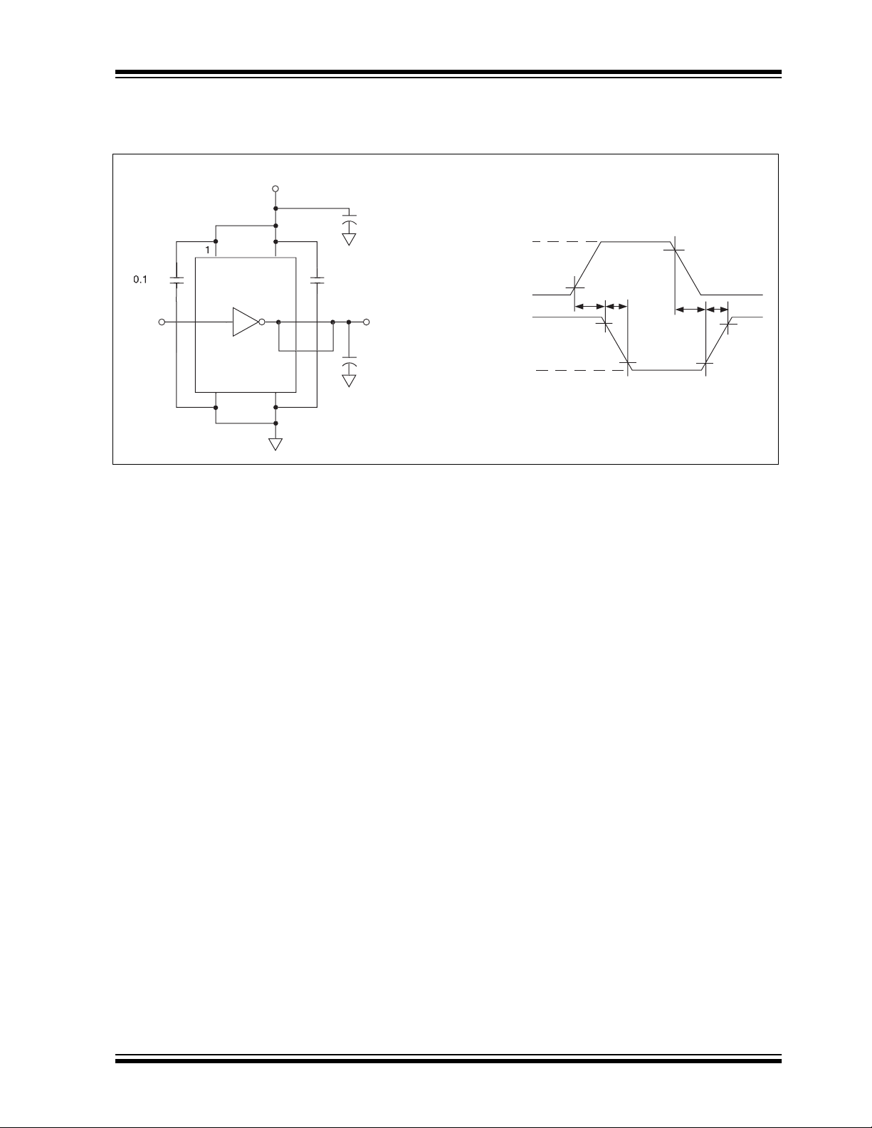
3.0 APPLICATIONS INFORMATION
1
6
5
pF
1
1
t
8V
put
FIGURE 3-1: SWITCHING TIME TEST CIRCUITS
= 1
.
0.1
Inpu
TC442
.
Out
= 10,000
+5V
Input
0V
+18V
Output
0V
Input: 100kHz,
square wave,
= t
t
RISE
TC4421/TC4422
90%
FALL
10%
≤ 10nsec
t
90%
D1
t
F t
10%
D2
10%
t
R
90%
2002 Microchip Technology Inc. DS21420B-page 5

TC4421/TC4422
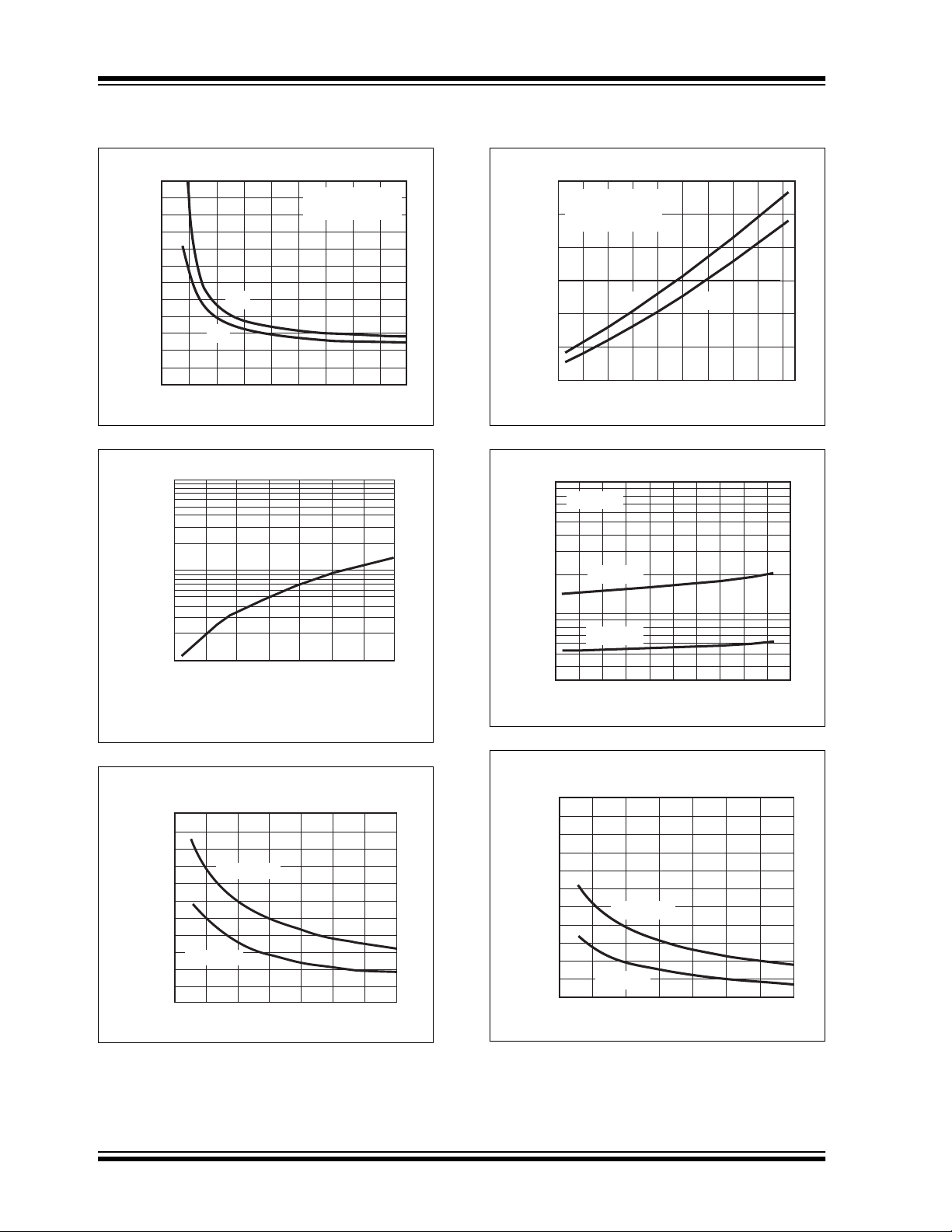
4.0 TYPICAL CHARACTERISTICS
Note: The graphs and tables provided following this note are a statistical summary based on a limited number of
samples and are pro vided for information al purposes only. The performa nce characteristic s listed herein ar e
not tested or guaranteed. In some graphs or tables, the data presented may be outside the specified
operating range (e.g., outside specified power supply range) and therefore outside the warranted range.
220
200
180
160
140
120
(nsec)
100
RISE
t
80
60
40
20
0
4681012
22,000pF
10,000pF
4700pF
1000pF
Rise TIme vs. Capacitive Load
300
250
200
150
(nsec)
RISE
t
100
Rise Time vs. Supply Voltage
180
160
140
120
100
(nsec)
80
FALL
t
60
4700pF
40
20
1000pF
0
V
DD
14 16 18
(V)
4 6 8 101214 1618
22,000pF
10,000pF
V
(V)
DD
Fall TIme vs. Capacitive Load
300
Fall Time vs. Supply Voltage
5V
10V
15V
10V
5V
15V
250
200
150
(nsec)
FALL
t
100
50
0
100 1000 10,000 100,000
C
LOAD
(pF)
Rise and Fall Times vs. Temperature
90
= 10,000pF
C
LOAD
V
80
70
60
TIME (nsec)
50
40
30
= 15V
DD
t
RISE
t
FALL
-40 0 40 80 120
(
T
°C)
A
50
0
100 1000 10,000
C
LOAD
(pF)
Propagation Delay vs. Supply Voltage
50
C
= 1000pF
LOAD
45
40
35
TIME (nsec)
30
25
t
D1
6
t
D2
810121416184
V
(V)
DD
100,000
DS21420B-page 6 2002 Microchip Technology Inc.

TYPICAL CHARACTERISTICS (CONTINUED)
TC4421/TC4422
Supply Current vs. Capacitive Load
220
200
2MHz
180
160
140
(mA)
120
100
SUPPLY
I
1.125MHz
80
632kHz
60
40
200kHz
20
0
100
C
LOAD
(pF)
Supply Current vs. Capacitive Load
180
VDD = 12V
160
140
120
100
(mA)
SUPPLY
I
2MHz
80
60
40
20
1.125MHz
632kHz
200kHz
0
100 100,00010,0001000
C
LOAD
(pF)
VDD = 18V
100,00010,0001000
63.2kHz
20kHz
63.2kHz
20kHz
Supply Current vs. Frequency
180
VDD = 18V
160
140
120
100
(mA)
80
SUPPLY
I
60
40
20
0
10 100 1000
0.1µF
47,000pF
10,000pF
FREQUENCY (kHz)
22,000pF
470pF
Supply Current vs. Frequency
180
VDD = 12V
160
140
120
100
(mA)
80
SUPPLY
I
60
0.1µF
40
20
0
10 100 1000
FREQUENCY (kHz)
22,000pF
10,000pF
47,000pF
4700pF
4700pF
470pF
Supply Current vs. Capacitive Load
100
VDD = 6V
90
80
70
60
(mA)
50
40
SUPPLY
I
2MHz
30
20
10
0
100 100,00010,0001000
632kHz
C
LOAD
(pF)
200kHz
63.2kHz
20kHz
(mA)
SUPPLY
I
Supply Current vs. Frequency
120
VDD = 6V
100
80
60
40
20
0
10
10 100 1000
4700pF
0.1µF
100 1000
FREQUENCY (kHz)
47,000pF
22,000pF
10,000pF
470pF
2002 Microchip Technology Inc. DS21420B-page 7
TC4421/TC4422
TYPICAL CHARACTERISTICS (CONTINUED)
Propagation Delay vs. Input Amplitude
120
110
100
90
80
70
60
50
TIME (nsec)
40
30
t
D2
t
D1
20
10
0
12345678910
INPUT (V)
Crossover Energy vs. Supply Voltage
-6
10
-7
10
A•sec
-8
10
4681012141618
NOTE: The values on this graph represent the loss seen
by the driver during a complete cycle. For the loss
in a single transition, divide the stated value by 2.
VDD = 10V
= 10,000pF
C
LOAD
V
(V)
DD
Propagation Delay vs. Temperature
50
VDD = 18V
C
= 10,000pF
LOAD
45
V
= 5V
IN
40
35
TIME (nsec)
30
25
20
t
D2
-40 -20 0 20 40 60 80 100 120-60
T
t
D1
(
°C)
A
Quiescent Supply Current vs. Temperature
3
10
VDD = 18V
(µA)
INPUT = 1
2
10
QUIESCENT
I
INPUT = 0
-40 -20 0 20 40 60 80 100 120-60
(
T
°C)
J
Low-State Output Resistance
High-State Output Resistance
vs. Supply Voltage
6
5.5
5
4.5
4
(Ω)
3.5
3
DS(ON)
R
2.5
2
1.5
1
0.5
46 81012141618
T
= 150
°C
J
= 25
°C
T
J
V
(V)
DD
6
5.5
5
4.5
4
(Ω)
3.5
3
DS(ON)
R
2.5
2
1.5
1
0.5
46 81012141618
vs. Supply Voltage
= 150
°
C
T
J
T
= 25
°
C
J
V
(V)
DD
DS21420B-page 8 2002 Microchip Technology Inc.

5.0 PACKAGING INFORMATION
)
)
)
)
)
)
)
)
)
)
)
)
)
)
)
)
)
)
)
)
)
)
)
)
P
5.1 Package Marking Information
Package marking data not available at this time.
5.2 Package Dimensions
-Pin Plastic DI
TC4421/TC4422
.260 (6.60
.240 (6.10
.045 (1.14
.030 (0.76
.200 (5.08
.140 (3.56
.150 (3.81
.115 (2.92
.400 (10.16
.348 (8.84
.110 (2.79
.090 (2.29
.070 (1.78
.040 (1.02
.022 (0.56
.015 (0.38
.040 (1.02
.020 (0.51
.310 (7.87
.290 (7.37
.015 (0.38
.008 (0.20
.400 (10.16
.310 (7.87
Dimensions: inches (mm)
2002 Microchip Technology Inc. DS21420B-page 9

TC4421/TC4422
)
)
)
)
)
)
.
.
)
)
)
)
)
)
)
)
)
)
)
)
)
)
)
)
)
(
)
Package Dimensions (Continued)
8-Pin CERDIP (Narrow)
.110 (2.79
.090 (2.29
.300 (7.62
.230 (5.84
.055 (1.40) MAX
.200 (5.08
.160 (4.06
.200 (5.08
.125 (3.18
5-Pin TO-220
.117 (2.97)
.103
.293 (7.44)
.204 (5.18)
2.62
.400 (10.16
.370 (9.40
.065 (1.65
.045 (1.14
.415 (10.54)
.390 (9.91)
.020 (0.51
.016 (0.41
.020 (0.51) MIN
.040 (1.02
.020 (0.51
.150 (3.81
.156 (3.96)
.140 (3.56)
DIA.
.015 (0.38
.008 (0.20
.055 (1.40)
.045 (1.14)
.613 (15.57)
.569 (14.45)
.320 (8.13
.290 (7.37
.400 (10.16
.320 (8.13
Dimensions: inches (mm)
.185 (4.70)
.165 (4.19)
3
°
- 7.5°
5 PLCS.
.590 (14.99)
.482 (12.24)
.037 (0.95)
.025 (0.64)
.025 (0.64)
.012 (0.30)
PIN 1
.273 (6.93)
.072 (1.83)
.062 (1.57)
.115 (2.92)
.087 (2.21)
.263 (6.68)
Dimensions: inches (mm)
DS21420B-page 10 2002 Microchip Technology Inc.

TC4421/TC4422
Sales and Support
Data Sheets
Products supported by a preliminary Data Sheet may have an errata sheet describing minor operational differences and recommended workarounds. To determine if an errata sheet exists for a particular device, please contact one of the following:
1. Your local Microchip sales office
2. The Microchip Corporate Literature Center U.S. FAX: (480) 792-7277
3. The Microchip Worldwide Site (www.microchip.com)
Please specify which device, revision of silicon and Data Sheet (include Literature #) you are using.
New Customer Notification System
Register on our web site (www.microchip.com/cn) to receive the most current information on our products.
2002 Microchip Technology Inc. DS21420B-page11

TC4421/TC4422
NOTES:
DS21420B-page12 2002 Microchip Technology Inc.

TC4421/TC4422
Information contained in this publication regarding device
applications and the like is intended through suggestion only
and may be superseded by updates. It is your responsibility to
ensure that your application meets with your specifications.
No representation or warranty is given and no liability is
assumed by Microchip Technology Incorporated with respect
to the accuracy or use of such information, or infringement of
patents or other intellectual property rights arising from such
use or otherwise. Use of Microchip’s products as critical components in life support systems is not authorized except with
express written approval by Microchip. No licenses are conveyed, implicitly or otherwise, under any intellectual property
rights.
Trademarks
The Microchip name and logo, the Microchip logo, FilterLab,
EELOQ, microID, MPLAB, PIC, PICmicro, PICMASTER,
K
PICSTART, PRO MATE, SEEVAL and The Embedded Control
Solutions Company are registered trademarks of Microchip T echnology Incorporated in the U.S.A. and other countries.
dsPIC, ECONOMONITOR, FanSense, FlexROM, fuzzyLAB,
In-Circuit Serial Programming, ICSP, ICEPIC, microPort,
Migratable Memory, MPASM, MPLIB, MPLINK, MPSIM,
MXDEV, PICC, PICDEM, PICDEM.net, rfPIC, Select Mode
and T otal Endurance are trademarks of Microchip T echnology
Incorporated in the U.S.A.
Serialized Quick Turn Programming (SQTP) is a service mark
of Microchip Technology Incorporated in the U.S.A.
All other trademarks mentioned herein are property of their
respective companies.
© 2002, Microchip Technology Incorporated, Printed in the
U.S.A., All Rights Reserved.
Printed on recycled paper.
Microchip received QS-9000 quality system
certification for its worldwide headquarters,
design and wafer fabrication facilities in
Chandler and Tempe, Arizona in July 1999
and Mountain View, California in March 2002.
The Company’s quality system processes and
procedures are QS-9000 compliant for its
PICmicro
devices, Serial EEPROMs, micrope ri ph era ls,
non-volatile memory and ana l og pro duc ts. In
addition, Microchip’s quality system for the
design and manufacture of development
systems is ISO 9001 certified.
®
8-bit MCUs, KEELOQ
®
code hoppin g
2002 Microchip Technology Inc. DS21420B-page 13

M
WORLDWIDE SALES AND SERVICE
AMERICAS
Corporate Office
2355 West Chandler Blvd.
Chandler, AZ 85224-6199
Tel: 480-792-7200 Fax: 480-792-7277
Technical Support: 480-792-7627
Web Address: http://www.microchip.com
Rocky Mountain
2355 West Chandler Blvd.
Chandler, AZ 85224-6199
Tel: 480-792-7966 Fax: 480-792-7456
Atlanta
500 Sugar Mill Road, Suite 200B
Atlanta, GA 30350
Tel: 770-640- 0034 Fax: 770-640-0307
Boston
2 Lan Drive, Suite 120
Westford, MA 01886
Tel: 978-692- 3848 Fax: 978-692-3821
Chicago
333 Pierce Road, Suite 180
Itasca, IL 60143
Tel: 630-285-0071 Fax: 630-285-0075
Dallas
4570 Westgrove Drive, Suite 160
Addison, TX 75001
Tel: 972-818- 7423 Fax: 972-818-2924
Detroit
Tri-Atria Office Building
32255 Northwestern Highway , Suite 190
Farmington Hills, MI 48334
Tel: 248-538-2250 Fax: 248-538-2260
Kokomo
2767 S. Albright Road
Kokomo, Indiana 46902
Tel: 765-864-8360 Fax: 765-864-8387
Los Angeles
18201 Von Karman, Suite 1090
Irvine, CA 92612
Tel: 949-263- 1888 Fax: 949-263-1338
New York
150 Motor Parkway, Suite 202
Hauppauge, NY 11788
Tel: 631-273- 5305 Fax: 631-273-5335
San Jose
Microchip Technology Inc.
2107 North First Street, Suite 590
San Jose, CA 95131
Tel: 408-436- 7950 Fax: 408-436-7955
Toronto
6285 Northam Drive, Suite 108
Mississauga, Ontario L4V 1X5, Cana da
Tel: 905-673-0699 Fax: 905-673-6509
ASIA/PACIFIC
Australia
Microchip Technology Australia Pty Ltd
Suite 22, 41 Rawson Street
Epping 2121, NSW
Australia
Tel: 61-2-9868-6733 Fax: 61-2-9868-6755
China - Beij ing
Microchip Technology Consulting (Shanghai)
Co., Ltd., Beijing Liaison Office
Unit 915
Bei Hai Wan Tai Bldg.
No. 6 Chaoyangmen Beidajie
Beijing, 100027, No. China
Tel: 86-10-85282100 Fax: 86-10-85282104
China - Chengdu
Microchip Technology Consulting (Shanghai)
Co., Ltd., Chengdu Liaison Office
Rm. 2401, 24th Floor,
Ming Xing Financial Tower
No. 88 TIDU Street
Chengdu 610016, China
Tel: 86-28-6766200 Fax: 86-28-6766599
China - Fuzhou
Microchip Technology Consulting (Shanghai)
Co., Ltd., Fuzhou Liaison Office
Unit 28F, World Trade Plaza
No. 71 Wusi Road
Fuzhou 350001, China
Tel: 86-591-7503506 Fax: 86-591-7503521
China - Shanghai
Microchip Technology Consulting (Shanghai)
Co., Ltd.
Room 701, Bldg. B
Far East International Plaza
No. 317 Xian Xia Road
Shanghai, 200051
Tel: 86-21-6275-5700 Fax: 86-21-6275-5060
China - Shenzhen
Microchip Technology Consulting (Shanghai)
Co., Ltd., Shenzhen Liaison Office
Rm. 1315, 13/F, Shenzhen Kerry Centre,
Renminnan Lu
Shenzhen 518001, China
Tel: 86-755-2350361 Fax: 86-755-2366086
Hong Kong
Microchip Technology Hongkong Ltd.
Unit 901-6, Tower 2, Metroplaza
223 Hing Fong Road
Kwai Fong, N.T., Hong Kong
Tel: 852-2401-1200 Fax: 852-2401-3431
India
Microchip Technology Inc.
India Liaison Office
Divyasree Chambers
1 Floor, Wing A (A3/A4)
No. 11, O’Shaugnessey Road
Bangalore, 560 025, India
Tel: 91-80-2290061 Fax: 91-80-2290062
Japan
Microchip Technology Japan K.K.
Benex S-1 6F
3-18-20, Shinyokohama
Kohoku-Ku, Yokohama-shi
Kanagawa, 222-0033, Japan
Tel: 81-45-471- 6166 Fax: 81-45-471-6122
Korea
Microchip Technology Korea
168-1, Youngbo Bldg. 3 Floor
Samsung-Dong, Kangnam-Ku
Seoul, Korea 135-882
Tel: 82-2-554-7200 Fax: 82-2-558-5934
Singapore
Microchip Technology Singapore Pte Ltd.
200 Middle Road
#07-02 Prime Centre
Singapore, 188980
Tel: 65-6334-8870 Fax: 65-6334-8850
Taiwan
Microchip Technology Taiwan
11F-3, No. 207
Tung Hua North Road
Taipei, 105, Taiwan
Tel: 886-2-2717-7175 Fax: 886-2-2545-0139
EUROPE
Denmark
Microchip Technology Nordic ApS
Regus Business Centre
Lautrup hoj 1-3
Ballerup DK-2750 Denmark
Tel: 45 4420 9895 Fax: 45 4420 9910
France
Microchip Technology SARL
Parc d’Activite du Moulin de Massy
43 Rue du Saule Trapu
Batiment A - ler Etage
91300 Massy, France
Tel: 33-1-69-53-63-20 Fax: 33-1-69-30-90-79
Germany
Microchip Technology GmbH
Gustav-Heinemann Ring 125
D-81739 Munich, Germany
Tel: 49-89-627-144 0 Fax: 49-89-627-144-44
Italy
Microchip Technology SRL
Centro Direzionale Colleoni
Palazzo Taurus 1 V. Le Colleoni 1
20041 Agrate Brianza
Milan, Italy
Tel: 39-039-65791-1 Fax: 39-039-6899883
United Kingdom
Arizona Microchip Technology Ltd.
505 Eskdale Road
Winnersh Triangle
Wokingham
Berkshire, England RG41 5TU
Tel: 44 118 921 5869 Fax: 44-118 921-5820
03/01/02
'!$'
DS21420B-page 14 2002 Microchip Technology Inc.
 Loading...