

Datasheet TC4405EPA, TC4405EOA, TC4405CPA, TC4405COA, TC4405MJA Datasheet (Microchip Technology)
...
M
8
6
5
OM
OP
OM
OP
8
6
5
OM
OP
OM
OP
8
/SOIC/C
P
1.5A Dual Open-Drain MOSFET Drivers
TC4404/TC4405
Features
• Independently Programmable Rise and Fall
Times
• Low Output Impedance – 7Ω Typ.
• High Speed t
, tF – <30nsec with 1000pF Load
R
• Short Delay Times – <30nsec
• Wide Operating Range
- 4.5V to 18V
• Latch-Up Protected: Will Withstand > 500mA
Reverse Current (Either Polarity)
• Input Withstands Negative Swings Up to -5V
Applications
• Motor Controls
• Driving Bipolar Transistors
• Driver for Non-overlapping Totem Poles
• Reach-Up/Reach-Down Driver
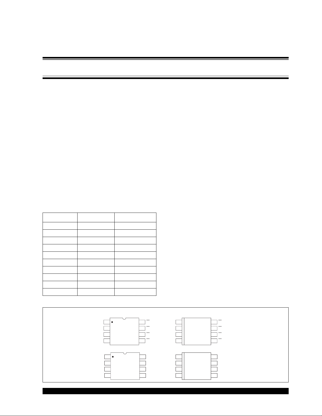
Device Selection Table
Part Number Package Temp. Range
TC4404COA 8-Pin SOIC 0°C to +70°C
TC4404CPA 8-Pin PDIP 0°C to +70°C
TC4404EOA 8-Pin SOIC -40°C to +85°C
TC4404EPA 8-Pin PDIP -40°C to +85°C
TC4404MJA 8-Pin CERDIP -55°C to +125°C
TC4405COA 8-Pin SOIC 0°C to +70°C
TC4405CPA 8-Pin PDIP 0°C to +70°C
TC4405EOA 8-Pin SOIC -40°C to +85°C
TC4405EPA 8-Pin PDIP -40°C to +85°C
TC4405MJA 8-Pin CERDIP -55°C to +125°C
General Description
The TC4404/TC4405 are CMOS buffer-drivers
constructed with comple mentary MOS ou tputs, wher e
the drains of the totem-pole output have been left
separated so that individual connections can be made
to the pull-up and pull-down sec tions of the o utput. This
allows the inserti on of d rain - cu rren t-li mi tin g res is to rs in
the pull-up and/ or pull-do wn sectio ns, allo wing the user
to define the r at es of r is e an d fa ll fo r a capac i ti ve lo ad ;
or a reduced outpu t s w ing , if dri vi ng a resistive load, or
to limit base current, when driving a bipolar transistor.
Minimum rise and fall times, with no resistors, will be
less than 30nsec for a 1000pF load.
For driving MOSFETs in motor-control applications,
where slow-ON/fast-OFF operation is desired, these
devices are superior to the previously used technique
of adding a diode-resistor combination between the
driver output and the MOSFET, because they allow
accurate control of tu rn-ON, while maintaining fast turnOFF and maximum noise immu nity for an OFF device.
When used to drive bipolar transistors, these drivers
maintain the high speeds common to other Microchip
drivers. They allow insertion of a base current-limiting
resistor, while pr ovidi ng a se parate half-o utpu t for f ast
turn-OFF. By proper positioning of the resistor, either
npn or pnp transistors can be driven.
For driving many loads in low-power regimes, these
drivers, beca use th ey el imi nate shoot-through currents
in the output stage, require significantly less power at
higher frequencies, and can be helpful in meeting
low-power budgets.
Package Type
-Pin PDIP
V
DD
1
2
IN A
IN B
GND
V
IN A
IN B
DD
TC4404
3
4
18
27
TC4405
36
45
A T
A BOTT
B T
B BOTT
A TOP
A BOTTOM
B TOP
B BOTTOMGND
2002 Microchip Technology Inc. DS21418B-page 1
ERDI
V
DD
1
2
IN A
IN B
GND
V
IN A
IN B
DD
TC4404
3
4
18
27
TC4405
36
45
A T
A BOTT
B T
B BOTT
A TOP
A BOTTOM
B TOP
B BOTTOMGND
TC4404/TC4405
Because neither drain i n an outp ut is depen dent o n the
other, these devices can also be used as open-drain
buffer/drivers where both drains are available in one
device, thus minimizing chip count. Unused open
drains shou ld be returned to the supply rail that their
device sources are connected to (pull-downs to
ground, pul l-ups to V
), to prevent static damage. In
DD
addition, in situations where timing resistors or other
means of limiting crossover currents are used, like
drains may be paralleled for gr eater current carrying
capacity.
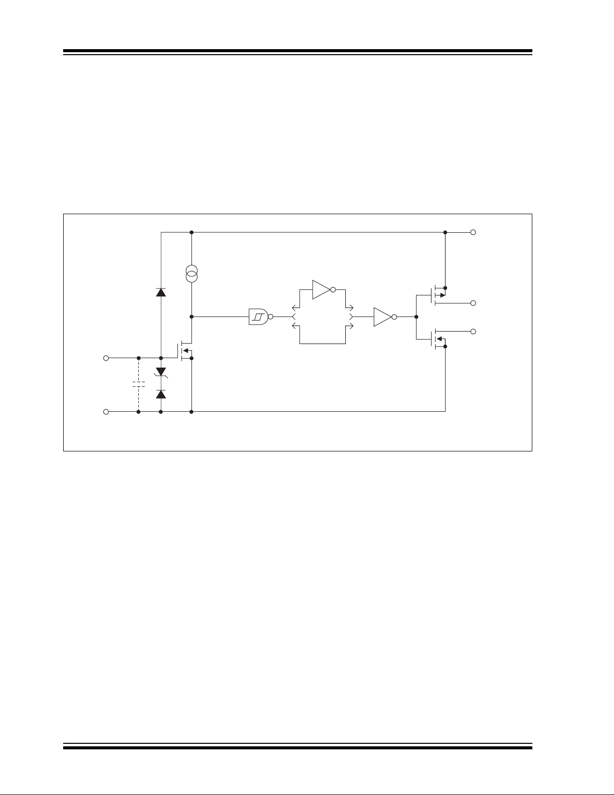
Functional Block Diagram
300 mV
2 (3)
Input
4.7V
These devices are built to operate in the mos t demanding electrical enviro nments. They will not latch up under
any conditions within their power and voltage ratings;
they are not subje ct to d am age when up to 5V of noise
spiking of either polarity occurs on their ground pin; an d
they can accept, without damage or logic upset, up to
1/2 amp of reverse current (of either polarity) being
forced back into their outputs. All terminals are fully
protected against up to 2kV of electrostatic discharge.
1
V
DD
TC4404
Inverting
8 (6)
Pull Up
7 (5)
Pull Down
TC4405
Noninverting
GND
4
Effective
Input
C ≤ 12 pF
A (B)
DS21418B-page 2 2002 Microchip Technology Inc.
TC4404/TC4405
1.0 ELECTRICAL
CHARACTERISTICS
Absolute Maximum Ratings*
Supply Voltage.....................................................+22V
*Stresses above those listed under "Absolute Maximum
Ratings" may cause permanent damage to the device. These
are stress ratings only and functional operation of the device
at these or any other conditions above those indicated in the
operation sections of the specifications is not implied.
Exposure to Absolute Maximum Rating conditions for
extended periods may affect device reliability.
Power Dissipation (TA ≤ 70°C)
PDIP........................................................ 730mW
CERDIP................................................... 800mW
SOIC........................................................ 470mW
Package Thermal Resistance
PDIP R
PDIP R
CERDIP R
CERDIP R
SOIC R
SOIC R
............................................. 125°C/W
θJ-A
............................................... 45°C/W
θJ-C
.........................................150°C/W
θJ-A
......................................... 55°C/W
θJ-C
............................................ 155°C/W
θJ-A
.............................................. 45°C/W
θJ-C
Operating Temperature Range
C Version.........................................0°C to +70°C
E Version..................................... -40°C to +85°C
M Ve rsion................................... -55°C to +125°C
Storage Temperature Range ............. -65°C to +150°C
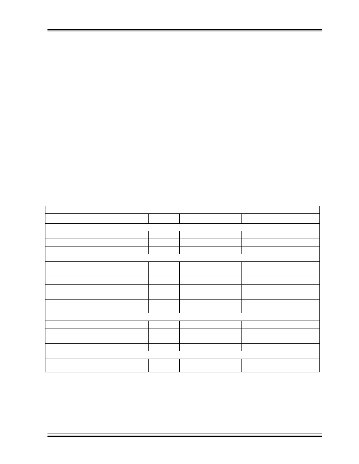
TC4404/TC4405 ELECTRICAL SPECIFICATIONS
Electrical Characteristics: TA = +25°C, with 4.5V ≤ V
Symbol Parameter Min Typ Max Units Test Conditions
Input
V
V
I
IN
Output
V
V
R
I
PK
I
DC
I
R
Switching Ti me (Note 1)
t
R
t
F
t
D1
t
D2
Power Supply
I
S
Note 1: Switching times ensured by design.
Logic 1, High Input Voltage 2.4 —— V
IH
Logic 0, Low Input Voltage ——0.8 V
IL
Input Current -1 — 1 µA0V ≤ V
High Output Voltage VDD – 0.025 —— V
OH
Low Output Voltage ——0.025 V
OL
Output Resistance — 710Ω I
O
Peak Output Current (Any Drain) — 1.5 — A Duty cycle ≤ 2%, t ≤ 300µsec
Continuous Output Current (Any Drain) ——100 mA
Latch-Up Protection (Any Drain)
Withstand Reverse Current
Rise Time — 25 30 nsec Figure 3-1, CL = 1000pF
Fall Time — 25 30 nsec Figure 3-1, CL = 1000pF
Delay Time — 15 30 nsec Figure 3-1, CL = 1000pF
Delay Time — 32 50 nsec Figure 3-1, CL = 1000pF
Power Supply Current —
≤ 18V, unless otherwise noted.
DD
≤ V
IN
DD
= 10mA, VDD = 18V; Any Drain
OUT
— >500 — mA Duty cycle ≤ 2%, t ≤ 300µsec
—
—
—
4.5
0.4
mA VIN = 3V (Both Inputs)
= 0V (Both Inputs)
V
IN
2002 Microchip Technology Inc. DS21418B-page 3
TC4404/TC4405
TC4404/TC4405 ELECTRICAL SPECIFICATIONS (CONTINUED)
Electrical Characteristics: Over operating temperature range with 4.5V ≤ V
Symbol Parameter Min Typ Max Units T est Conditions
V
V
I
IN
Logic 1, High Input Voltage 2.4 —— V
IH
Logic 0, Low Input Voltage ——0.8 V
IL
Input Current -10 — 10 µA0V ≤ V
Output
V
V
R
I
PK
I
DC
I
R
High Output Voltage VDD – 0.025 —— V
OH
Low Output Voltage ——0.025 V
OL
Output Resistance — 912Ω I
O
Peak Output Current (Any Drain) — 1.5 — A Duty cycle ≤ 2%, t ≤ 300µsec
Continuous Output Current (Any Drain) ——100 mA
Latch-Up Protection (Any Drain)
— >500 — mA Duty cycle ≤ 2%, t ≤ 300µsec
Withstand Reverse Current
Switching Time (Note 1)
t
R
t
F
t
D1
t
D2
Rise Time ——40 nsec Figure 3-1, CL = 1000pF
Fall Time ——40 nsec Figure 3-1, CL = 1000pF
Delay Time ——40 nsec Figure 3-1, CL = 1000pF
Delay Time ——60 nsec Figure 3-1, CL = 1000pF
Power Supply
I
S
Note 1: Switching times ensured by design.
Power Supply Current —
—
—
—
≤ 18V, unless otherwise noted.
DD
≤ V
IN
= 10mA, VDD = 18V; Any Drain
OUT
8
0.6
mA VIN = 3V (Both Inputs)
= 0V (Both Inputs)
V
IN
DD
DS21418B-page 4 2002 Microchip Technology Inc.
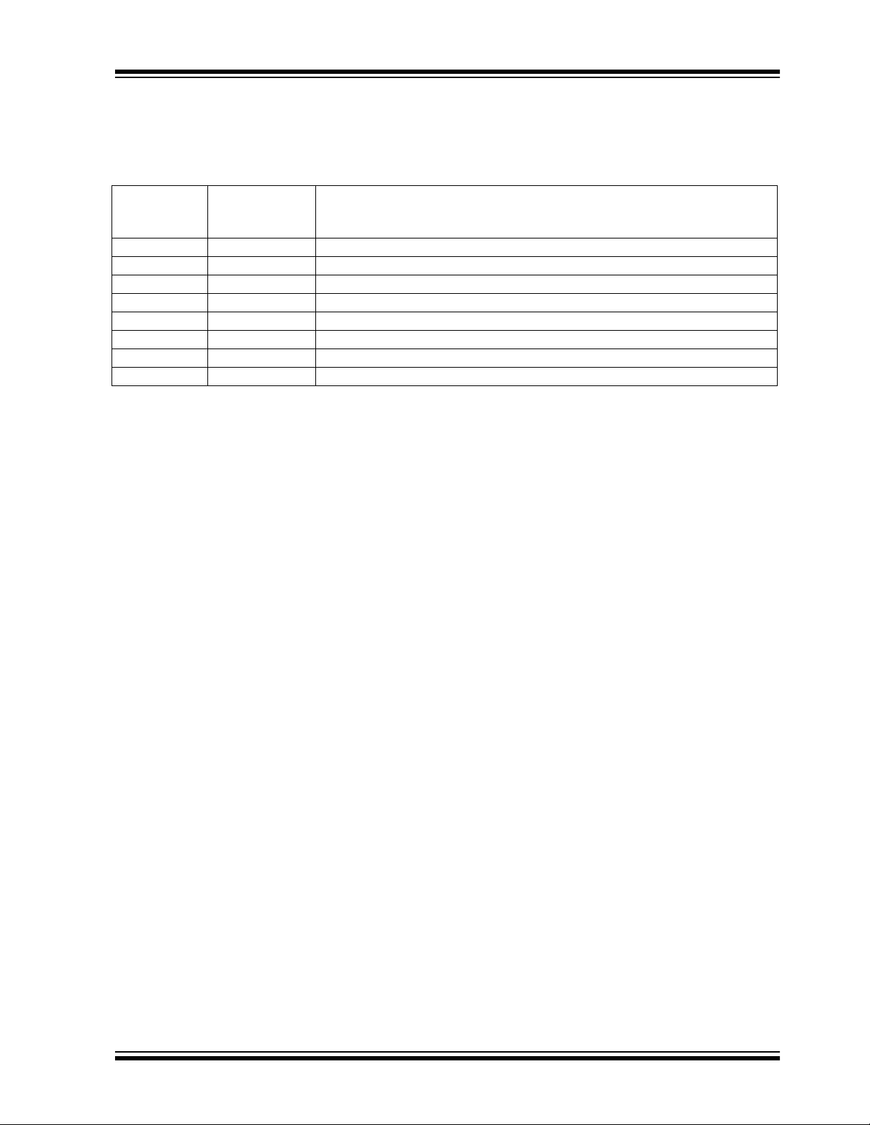
2.0 PIN DESCRIPTIONS
The descriptions of the pins are listed in Table 2-1.
TABLE 2-1: PIN FUNCTION TABLE
Pin No.
(8-Pin PDIP,
SOIC, CERD IP)
1V
2 IN A Control input A, TTL/CMOS compatible input.
3 IN B Control input A, TTL/CMOS compatible input.
4 GND Ground.
5 B BOTTOM Output B, pull down.
6 B TOP Output B, pull up.
7 A BOTTOM Output A, pull down.
8 A TOP Output A, pull up.
Symbol Description
DD
Supply input, 4.5V to 18V.
TC4404/TC4405
2002 Microchip Technology Inc. DS21418B-page 5

TC4404/TC4405
3.0 APPLICATIONS INFORMATION
3.1 Circuit Layout Guidelines
Avoid long power supply and ground traces (added
inductance causes unwanted voltage transients). Use
power and ground planes wherever possible. In
FIGURE 3-1: SWITCHING TIME TEST CIRCUITS
+5V
Input
V
= 18V
DD
18V
Output
+5V
Input
Input
1
2 8,7
1
2
0.1µF4.7µF
Output
CL = 1000pF
addition, it is advisable t hat lo w ESR byp ass cap acitor s
(4.7µF or 10µF tantalum) be placed as close to the
driver as possible. The driver should be physically
located as close to the device it is driving as possible to
minimize the length of the output trace.
90%
10%
0V
0V
t
D1
90%
10%
t
t
F
D2
t
R
10%
90%
Inverting Driver
90%
4
Input: 100kHz,
square wave,
= t
FALL
≤ 10nsec
t
RISE
3.2 Typical Applications
FIGURE 3-2: ZERO CROSSOVER
CURRENT TOTEM-POLE
SWITCH
V
(4.5V - 18V)
DD
From TTL
GND
TC4404
R
T
R
T
V
OUT
10%
0V
18V
Output
0V
90%
t
D1
10%
t
R
Noninverting Driver
FIGURE 3-3: DRIVING BIPOLAR
TRANSISTORS
V
(4.5V - 18V)
From TTL
DD
TC4405
GND
D2
10%
90%
t
F
t
R
IB
R
IB
DS21418B-page 6 2002 Microchip Technology Inc.

FIGURE 3-4: SERVO MOTOR CONTROL
+24V
TC4404/TC4405
+12V
15V
Direction
(TTL Level)
Speed
(PWM)
GND
TC4404TC4469
FIGURE 3-5: REACH-UP AND REACH-DOWN DRIVING
+12V
47kΩ
R
T
R
T
47kΩ
0.1µF 0.1µF
I
SENSE
+12V
15V
Motor
+5V
From TTL
GND
-12V
Switched
+12V
+5V
TC4404
GND
Switched
-12V
-12V
2002 Microchip Technology Inc. DS21418B-page 7

TC4404/TC4405
ge
S
(
)
6
810
16
18
pF
470 pF
pF
1500 pF
00
80
60
0
0
0
1000 pF
p
(
)
0
8
pF
p
pF
00
0
0
d
001000
0
D
)
0V
5V
S
(
)
00
0
0
) (V)
T
5
5
es
y
ge
d
0
0
0
0
8
(
)
)
(
)
)
0
0
0
352545105125-15
(
)
001000
0
00
0
0
D
)
t
t
5V
pF
5V
pF
t
SE
ge
)
(
)
81016
(
)
)
50
0
30
0
0
(
)
0
y
e
e
5
52545105125
1
0
0
)
1
t
5
D
pF
5V
pF
t
t
0
0
0
4.0 TYPICAL CHARACTERISTICS
Note: The graphs and tables provided following this note are a statistical summary based on a limited number of
samples and are pro vided for information al purposes only. The performance chara cteristics listed h erein are
not tested or guaranteed. In some graphs or tables, the data presented may be outside the specified
operating range (e.g., outside specified power supply range) and therefore outside the warranted range.
Rise Time vs. Supply Voltage
1
nsec
E
I
2200
4
2
100
(V
Fall Time vs. Capacitive Loa
1
nsec
4
2
1
LOA
(pF
10V
15V
= +2
=
10,00
Fall Time vs. Supply Volta
1
nsec
2200
4
2
100
1
Rise and Fall Tim
vs. Temperature
= 1000
= 17.
4
nsec
IME
2
1
-55-
t
FALL
Rise TIme vs. Capacitive Loa
1
= +2
161
nsec
E
I
4
2
1
LOA
(pF
1
1
10,00
Propagation Dela
vs. Supply Volta
= 1000
nsec
4
ELAY TIME
2
RI
1
C
D2
1
(V
161
Effect of Input Amplitude
on Dela
nsec
4
ELAY TIME
2
1
t
LOA
D2
Tim
(V
= 1000
1
Propagation Delay Time
vs. Temperatur
= 17.
= 1000
nsec
4
ELAY TIME
2
1
-55-35-1
Quiescent Supply Current
vs. Volta
1
= +2
BOTH INPUTS =
mA
UIESCENT
BOTH INPUTS =
.
C
(V
1
DS21418B-page 8 2002 Microchip Technology Inc.

TYPICAL CHARACTERISTICS (CONTINUED)
Quiescent Supply Current
4.0
vs. Temperature
VDD = 18V
BOTH INPUTS = 1
3.5
(mA)
3.0
QUIESCENT
I
2.5
2.0
-55 -35 -15 5 25 45 65 85 105
TEMPERATURE (°C)
125
Pull-Up Output Resistance
25
20
WORST CASE
(Ω)
15
DS(ON)
R
10
8
5
4681012
@ T
TYP @ +25°C
= +150°C
J
14 16
TC4404/TC4405
Pull-Down Output Resistance
25
20
(Ω)
15
DS(ON)
R
10
8
5
18
4681012
WORST CASE
@ T
= +150°C
J
TYP @ +25°C
(V)VDD (V)
V
DD
14 16
18
2002 Microchip Technology Inc. DS21418B-page 9

TC4404/TC4405
)
)
)
)
)
)
)
)
)
)
)
)
)
)
)
)
)
)
)
)
)
)
)
)
P
5.0 PACKAGING INFORMATION
5.1 Package Marking Information
Package mar k ing data not available at this time.
5.2 Package Dimensions
-Pin Plastic DI
.260 (6.60
.240 (6.10
.045 (1.14
.030 (0.76
.200 (5.08
.140 (3.56
.150 (3.81
.115 (2.92
.400 (10.16
.348 (8.84
.110 (2.79
.090 (2.29
.070 (1.78
.040 (1.02
.022 (0.56
.015 (0.38
.040 (1.02
.020 (0.51
.310 (7.87
.290 (7.37
.015 (0.38
.008 (0.20
.400 (10.16
.310 (7.87
Dimensions: inches (mm)
DS21418B-page 10 2002 Microchip Technology Inc.

Package Dimensions (Continued)
)
)
)
)
)
)
.
.
)
)
)
)
)
)
)
)
)
)
)
)
)
)
)
)
)
.
)
)
)
)
)
)
)
)
)
)
)
)
)
)
)
)
C
8-Pin CERDIP (Narrow)
.110 (2.79
.090 (2.29
.300 (7.62
.230 (5.84
TC4404/TC4405
.055 (1.40) MAX
.200 (5.08
.160 (4.06
.200 (5.08
.125 (3.18
-Pin SOI
.400 (10.16
.370 (9.40
.065 (1.65
.045 (1.14
.157 (3.99
.150 (3.81
.020 (0.51
.016 (0.41
.244 (6.20
.228 (5.79
.020 (0.51) MIN
.040 (1.02
.020 (0.51
.150 (3.81
.015 (0.38
.008 (0.20
.320 (8.13
.290 (7.37
.400 (10.16
.320 (8.13
Dimensions: inches (mm)
.050 (1.27) TYP
.197 (5.00
.189 (4.80
.069 (1.75
.053 (1.35
.020 (0.51
.013 (0.33
2002 Microchip Technology Inc. DS21418B-page 11
.010 (0.25
.004 (0.10
.050 (1.27
.016 (0.40
Dimensions: inches (mm)
.010 (0.25
.007 (0.18

TC4404/TC4405
NOTES:
DS21418B-page 12 2002 Microchip Technology Inc.

TC4404/TC4405
Sales and Support
Data Sheets
Products supported by a preliminary Data Sheet may have an errata sheet describing minor operational differences and recommended workarounds. To determine if an errata sheet exists for a particular device, please contact one of the following:
1. Your local Microchip sales office
2. The Microchip Corporate Literature Center U.S. FAX: (480) 792-7277
3. The Microchip Worldwide Site (www.micr ochip.com)
Please specify which device, revision of silicon and Data Sheet (include Literature #) you are using.
New Customer Notification System
Register on our web site (www.microchip.com/cn) to receive the most current information on our products.
2002 Microchip Technology Inc. DS21418B-page13

TC4404/TC4405
NOTES:
DS21418B-page14 2002 Microchip Technology Inc.

TC4404/TC4405
Information contained in this publication regarding device
applications and the like is intended through suggestion only
and may be superseded by updates. It is your responsibility to
ensure that your application meets with your specifications.
No representation or warranty is given and no liability is
assumed by Microchip Technology Incorporated with respect
to the accuracy or use of such information, or infringement of
patents or other intellectual property rights arising from such
use or otherwise. Use of Microchip’s products as critical components in life support systems is not authorized except with
express written approval by Microchip. No licenses are conveyed, implicitly or otherwise, under any intellectual property
rights.
Trademarks
The Microchip name and logo, the Microchip logo, FilterLab,
EELOQ, microID, MPLAB, PIC, PICmicro, PICMASTER,
K
PICSTART, PRO MATE, SEEVAL and The Embedded Co ntrol
Solutions Company are registered trademarks of Microchip Technology Incorporated in the U.S.A. and other countries.
dsPIC, ECONOMONITOR, FanSense, FlexROM, fuzzyLAB,
In-Circuit Serial Programming, ICSP, ICEPIC, microPort,
Migratable Memory, MPASM, MPLIB, MPLINK, MPSIM,
MXDEV, PICC, PICDEM, PICDEM.net, rfPIC, Select Mode
and T otal Endurance are trademarks of Microchip T echnology
Incorporated in the U.S.A.
Serialized Quick Turn Programming (SQTP) is a service mark
of Microchip Technology Incorpora ted in the U.S.A.
All other trademarks mentioned herein are property of their
respective companies.
© 2002, Microchip Technology Incorporated, Printed in the
U.S.A., All Rights Reserved.
Printed on recycled paper.
Microchip received QS-9000 quality system
certification for its worldwide headquarters,
design and wafer fabrication facilities in
Chandler and Tempe, Arizona in July 1999
and Mountain View, California in March 2002.
The Company’s quality system processes and
procedures are QS-9000 compliant for its
PICmicro
devices, Serial EEPROMs, micrope ri ph era ls,
non-volatile memory and ana l og pro duc ts. In
addition, Microchip’s quality system for the
design and manufacture of development
systems is ISO 9001 certified.
®
8-bit MCUs, KEELOQ
®
code hoppin g
2002 Microchip Technology Inc. DS21418B-page 15

M
WORLDWIDE SALES AND SERVICE
AMERICAS
Corporate Office
2355 West Chandler Blvd.
Chandler, AZ 85224-6199
Tel: 480-792-7200 Fax: 480-792-7277
Technical Support: 480-792-7627
Web Address: http://www.microchip.com
Rocky Mountain
2355 West Chandler Blvd.
Chandler, AZ 85224-6199
Tel: 480-792-7966 Fax: 480-792-7456
Atlanta
500 Sugar Mill Road, Suite 200B
Atlanta, GA 30350
Tel: 770-640-0034 Fax: 770-640 -03 07
Boston
2 Lan Drive, Suite 120
Westford, MA 01886
Tel: 978-692-3848 Fax: 978-692 -38 21
Chicago
333 Pierce Road, Suite 180
Itasca, IL 60143
Tel: 630-285-0071 Fax: 630-285-0075
Dallas
4570 Westgrove Drive, Suite 160
Addison, TX 75001
Tel: 972-818-7423 Fax: 972-818 -29 24
Detroit
Tri-Atria Office Building
32255 Northwestern Highway, Suite 190
Farmington Hills, MI 48334
Tel: 248-538-2250 Fax: 248-538-2260
Kokomo
2767 S. Albright Road
Kokomo, Indiana 46902
Tel: 765-864-8360 Fax: 765-864-8387
Los Angeles
18201 Von Karman, Suite 1090
Irvine, CA 92612
Tel: 949-263-1888 Fax: 949-263 -13 38
New York
150 Motor Parkway, Suite 202
Hauppauge, NY 11788
Tel: 631-273-5305 Fax: 631-273 -53 35
San Jose
Microchip Technology Inc.
2107 North First Street, Suite 590
San Jose, CA 95131
Tel: 408-436-7950 Fax: 408-436 -79 55
Toronto
6285 Northam Drive, Suite 108
Mississauga, Ontario L4V 1X5, Cana da
Tel: 905-673-0699 Fax: 905-673-6509
ASIA/PACIFIC
Australia
Microchip Technology Australia Pty Ltd
Suite 22, 41 Rawson Street
Epping 2121, NSW
Australia
Tel: 61-2-9868-6733 Fax: 61-2-9868-6755
China - Beij ing
Microchip Technology Consulting (Shanghai)
Co., Ltd., Beijing Liaison Office
Unit 915
Bei Hai Wan Tai Bldg.
No. 6 Chaoyangmen Beidajie
Beijing, 100027, No. China
Tel: 86-10-85282100 Fax: 86-10-85282104
China - Chengdu
Microchip Technology Consulting (Shanghai)
Co., Ltd., Chengdu Liaison Office
Rm. 2401, 24th Floor,
Ming Xing Financial Tower
No. 88 TIDU Street
Chengdu 610016, China
Tel: 86-28-6766200 Fax: 86-28-6766599
China - Fuzhou
Microchip Technology Consulting (Shanghai)
Co., Ltd., Fuzhou Liaison Office
Unit 28F, World Trade Plaza
No. 71 Wusi Road
Fuzhou 350001, China
Tel: 86-591-7503506 Fax: 86-591-7503521
China - Shanghai
Microchip Technology Consulting (Shanghai)
Co., Ltd.
Room 701, Bldg. B
Far East Internationa l Plaza
No. 317 Xian Xia Road
Shanghai, 200051
Tel: 86-21-6275-5700 Fax: 86-21-6275-5060
China - Shenzhen
Microchip Technology Consulting (Shanghai)
Co., Ltd., Shenzhen Liaison Office
Rm. 1315, 13/F, Shenzhen Kerry Centre,
Renminnan Lu
Shenzhen 518001, China
Tel: 86-755-2350361 Fax: 86-755-2366086
Hong Kong
Microchip Technology Hongkong Ltd.
Unit 901-6, Tower 2, Metroplaza
223 Hing Fong Road
Kwai Fong, N.T., Hong Kong
Tel: 852-2401-1200 Fax: 852-2401-3431
India
Microchip Technology Inc.
India Liaison Office
Divyasree Chambers
1 Floor, Wing A (A3/A4)
No. 11, O’Shaugnessey Road
Bangalore, 560 025, India
Tel: 91-80-2290061 Fax: 91-80-2290062
Japan
Microchip Technology Japan K.K.
Benex S-1 6F
3-18-20, Shinyokohama
Kohoku-Ku, Yokohama-shi
Kanagawa, 222-0033, Japan
Tel: 81-45-471- 6166 Fax: 81-45-471-6122
Korea
Microchip Technology Korea
168-1, Youngbo Bldg. 3 Floor
Samsung-Dong, Kangnam-Ku
Seoul, Korea 135-882
Tel: 82-2-554-7200 Fax: 82-2-558-5934
Singapore
Microchip Technology Singapore Pte Ltd.
200 Middle Road
#07-02 Prime Centre
Singapore, 188980
Tel: 65-6334-8870 Fax: 65-6334-8850
Taiwan
Microchip Technology Taiwan
11F- 3, No. 2 07
Tung Hua North Road
Taipei, 105, Taiwan
Tel: 886-2-2717-7175 Fax: 886-2-2545-0139
EUROPE
Denmark
Microchip Technology Nordic ApS
Regus Business Centre
Lautrup hoj 1-3
Ballerup DK-2750 Denmark
Tel: 45 4420 9895 Fax: 45 4420 9910
France
Microchip Technology SARL
Parc d’Activite du Moulin de Massy
43 Rue du Saule Trapu
Batiment A - ler Etage
91300 Massy, France
Tel: 33-1-69-53-63-20 Fax: 33-1-69-30-90-79
Germany
Microchip Technology GmbH
Gustav-Heinemann Ring 125
D-81739 Munich, Germany
Tel: 49-89-627-144 0 Fax: 49-89-627-144-44
Italy
Microchip Technology SRL
Centro Direzionale Colleoni
Palazzo Taurus 1 V. Le Colleoni 1
20041 Agrate Brianza
Milan, Italy
Tel: 39-039-65791-1 Fax: 39-039-6899883
United Kingdom
Arizona Microchip Technology Ltd.
505 Eskdale Road
Winnersh Triangle
Wokingham
Berkshire, England RG41 5TU
Tel: 44 118 921 5869 Fax: 44-118 921-5820
03/01/02
'!$'
DS21418B-page 16 2002 Microchip Technology Inc.
 Loading...