

M
1.5A High-Speed, Floating Load Driver
TC4403
Features
• Low Quiescent Current: 300µA Max
• Capacitive Inputs With 300mV Hysteresis
• Both Inputs Must Be Driven to Drive Load
• Low Output Leakage
• High Peak Current Capability
• Fast Output Rise Time
• Outputs Individually Testable
Applications
• Isolated Load Drivers
•Pulsers
• Safety Interlocks
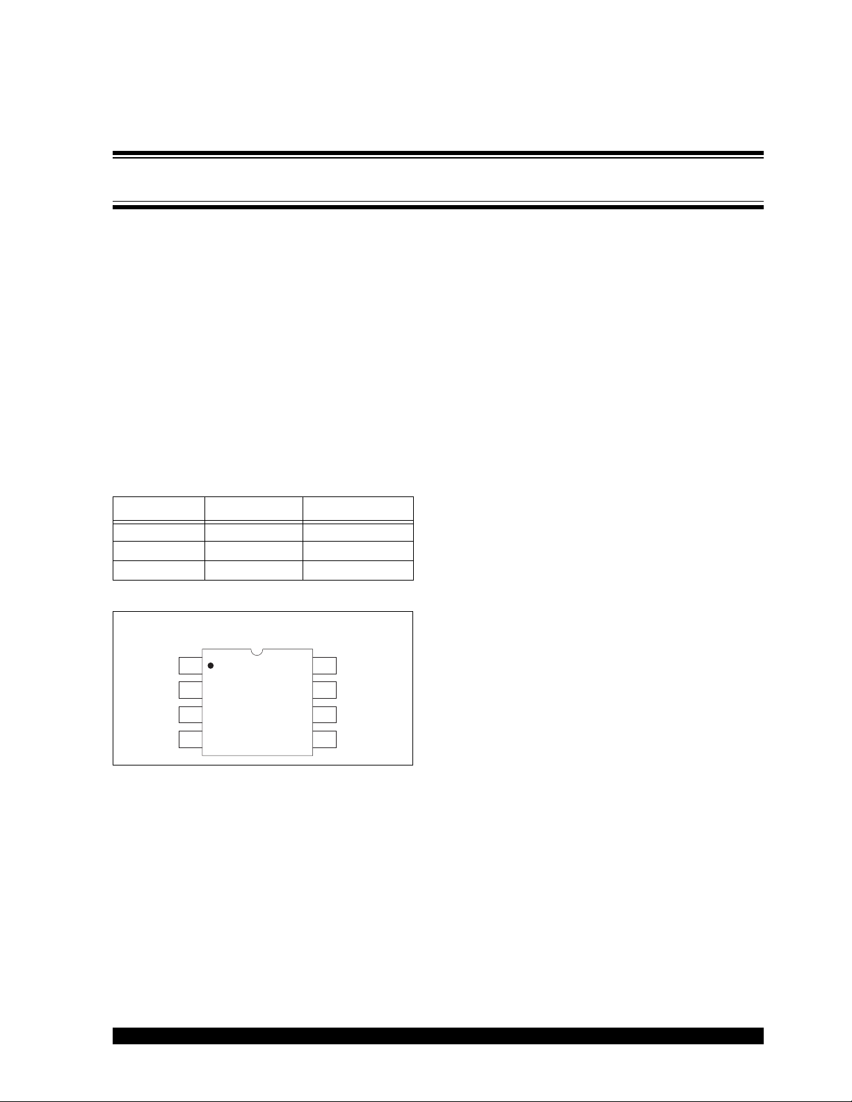
Device Selection Table
Part Number Package Temp. Range
TC4403CPA 8-Pin PDIP 0°C to +70°C
TC4403EPA 8-Pin PDIP -40°C to +85°C
TC4403MJA 8-Pin CERDIP -55°C to +125°C
Package Type
8-Pin PDIP/CERDIP
NC
OUT (VDD)
V
DD
OUT (GND)IN (GND)
IN (V
NC
18
27
)
DD
36
GND
45
TC4403
General Description
The TC4403 is a modified versi on of the TC4425 driver ,
intended to drive floating or isolated loads requiring
high-current pulses. The load is intended to be connected between the outputs without other reference to
supply or ground. Then, only when both logic inputs
and the V
the load. This construction allows the implementation
of a wide variety of redundant input controllers.
The low OFF-state output leakage and independence
of the two half-circuits permit a wide variety of testing
schemes to be utiliz ed to ass ure fun ctiona lity. The hig h
peak current capability, short internal delays, and fast
output rise and fall times ensure that sufficient power
will be available to th e load when i t is n eeded . The TT L
and CMOS compatible inputs allow operation from a
wide variety of input devices. The ability to swing the
inputs negative without affecting device performance
allows negative biases to be placed on the inputs for
greater safety. In addition, the capacitive nature of the
inputs allows the use of series resistors on the inputs
for extra noise suppression.
The TC4403 is built for outstanding ruggedness and
reliability in harsh applications. Input voltage excursions above the supply voltage or below ground are
clamped internally without damaging the device. The
output stages are power MOSFETs with high-speed
body diodes to prevent damage to the driver from
inductive kickbacks.
input are energized, is power supplied to
DD
2002 Microchip Technology Inc. DS21417B-page 1
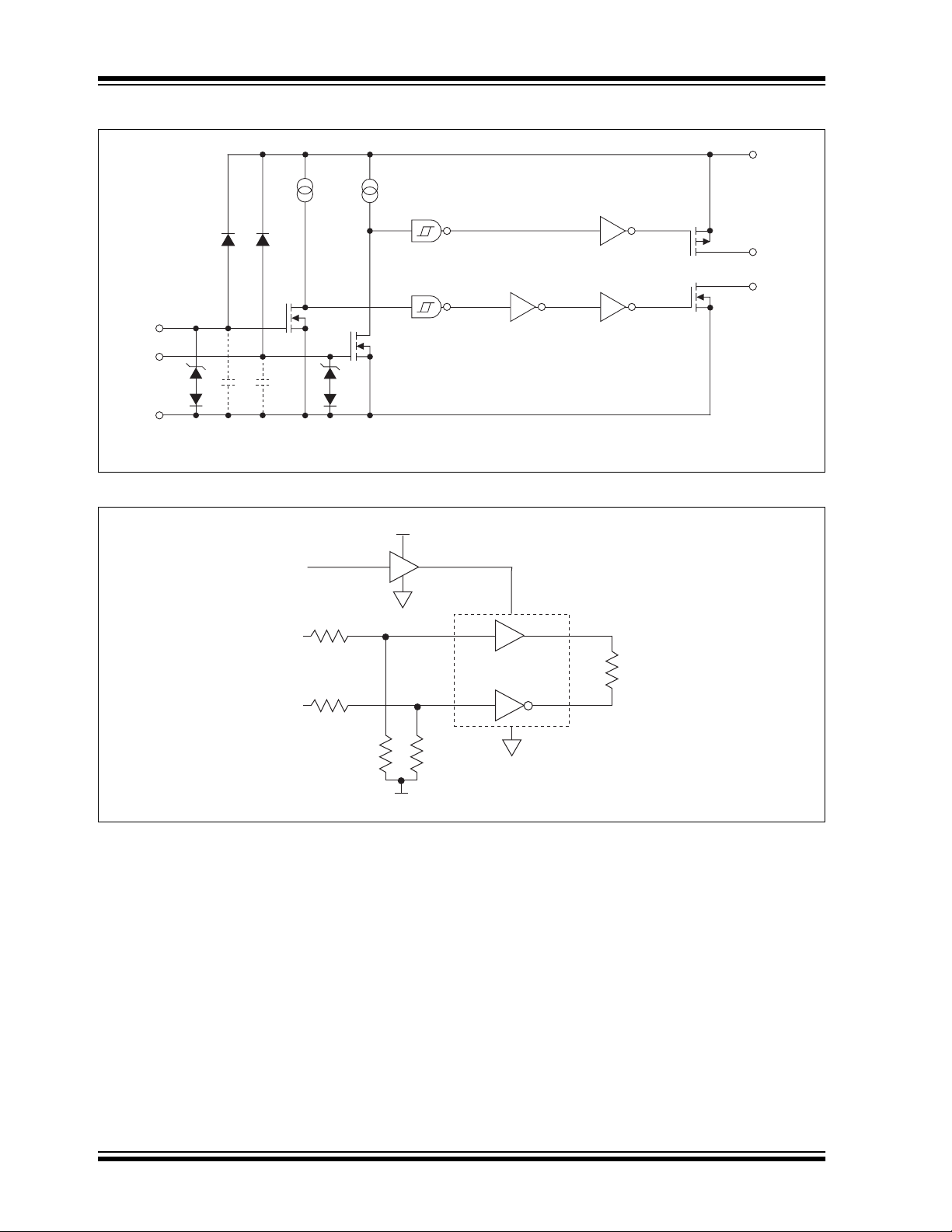
TC4403
Functional Block Diagram
300mV Input
Hysteresis
6
7
5
V
DD
OUT (V
DD
OUT (GND)
)
DD
GND
4
2
)
3
Effective Input
C = 20pF
(Each Input)
IN (GND)
IN (V
Typical Application
Power
Fire
Arm
TC4403
+15V
TC4422
6
R
T
R
T
1 MΩ
2
4
1 MΩ
6
TC4403
3
3
7
R
LOAD
5
-15V
DS21417B-page 2 2002 Microchip Technology Inc.

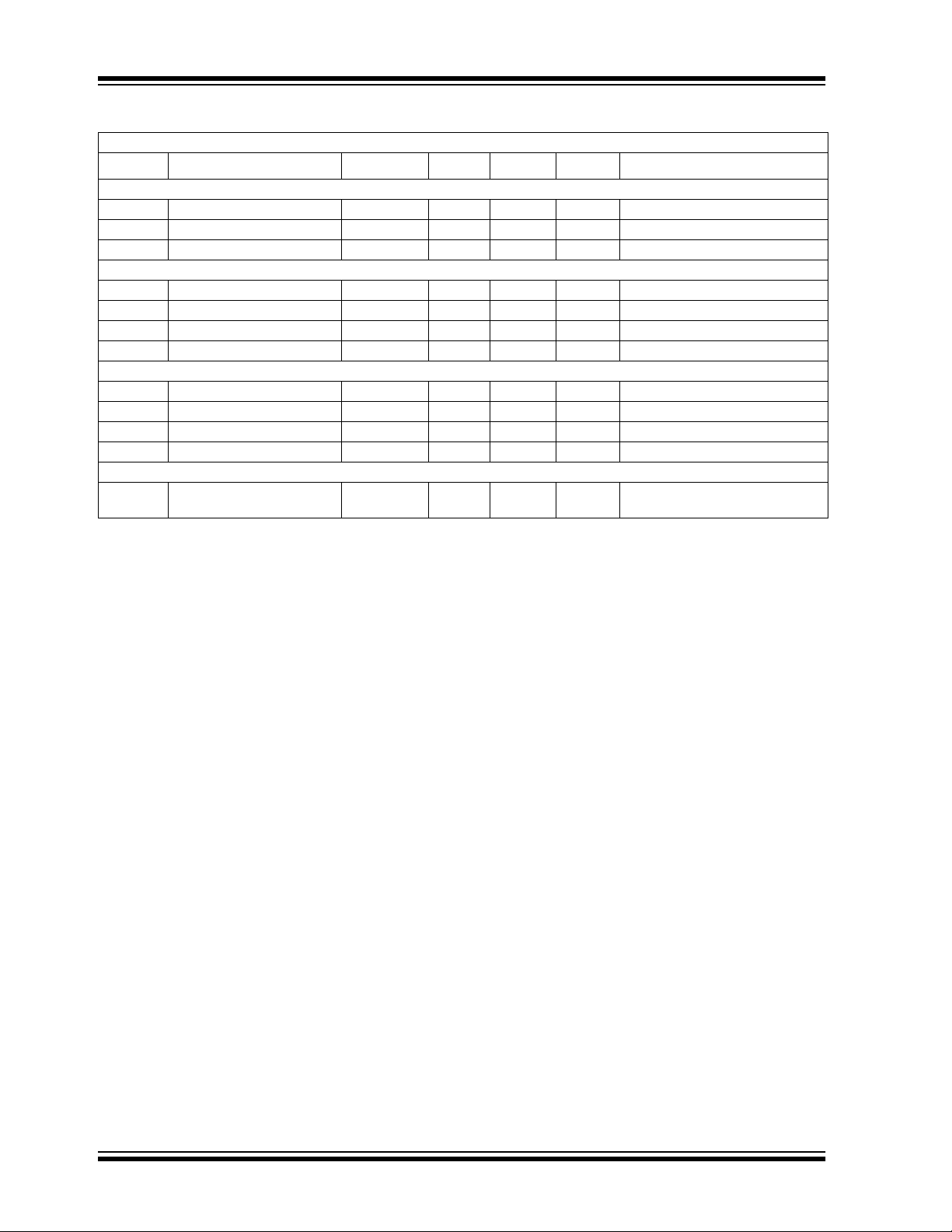
TC4403
1.0 ELECTRICAL
CHARACTERISTICS
Absolute Maximum Ratings*
Supply Voltage.....................................................+22V
*Stresses above those listed under "Absolute Maximum
Ratings" may cause permanent damage to the device. These
are stress ratings only and functional operation of the device
at these or any other conditions above those indicated in the
operation sections of the specifications is not implied.
Exposure to Absolute Maximum Rating conditions for
extended periods may affect device reliability.
Package Thermal Resistance
CERDIP R
CERDIP R
PDIP R
PDIP R
........................................ 150°C/W
θJ-A
......................................... 50°C/W
θJ-C
............................................. 125°C/W
θJ-A
............................................... 42°C/W
θJ-C
Operating Temperature Range
C Version.........................................0°C to +70°C
E Version..................................... -40°C to +85°C
M Version................................... -55°C to +125°C
Storage Temperature Range ............. -65°C to +150°C
TC4403 ELECTRICAL SPECIFICATIONS
Electrical Characteristics: TA = +25°C, with 4.5V ≤ V
Symbol Parameter Min Typ Max Units Tes t Conditions
Input
V
IH
V
IL
I
IN
Output
V
OH
V
OL
R
OS
R
OG
I
PK
Switching Ti me (Note 1)
t
R
t
F
t
D1
t
D2
Power Supply
I
S
Note 1: Switching times ensured by design.
Logic 1, High Input Voltage 2.4 —— V
Logic 0, Low Input Voltage ——0.8 V
Input Current -1000 ±10 ±1000 nA -5V ≤ V
High Output Voltage VDD – 0.025 —— V
Low Output Voltage ——0.025 V
Sourcing Output Resistance — 2.8 5 Ω I
Grounding Output Resistance — 3.5 5 Ω I
Peak Output Current — 1.5 — A
Rise Time — 23 35 nsec Figure 3-1, CL = 1800pF
Fall Time — 25 35 nsec Figure 3-1, CL = 1800pF
Delay Time — 33 75 nsec Figure 3-1, CL = 1800pF
Delay Time — 38 75 nsec Figure 3-1, CL = 1800pF
Power Supply Current —
≤ 18V, unless otherwise noted.
DD
1.5
—
0.15
2.5
0.25
≤ V
IN
DD
= 10mA, VDD = 18V
OUT
= -10mA, VDD = 18V
OUT
mA VIN = 3V (Both Inputs)
V
= 0V (Both Inputs)
IN
2002 Microchip Technology Inc. DS21417B-page 3
TC4403
TC4403 ELECTRICAL SPECIFICATIONS (CONTINUED)
Electrical Characteristics: Over operating temperature range with 4.5V ≤ V
Symbol Parameter Min Typ Max Units Test Conditions
Input
V
IH
V
IL
I
IN
Logic 1, High Input Voltage 2.4 —— V
Logic 0, Low Input Voltage ——0.8 V
Input Current -10,000 ±10 ±10,000 nA -5V ≤ V
Output
V
OH
V
OL
R
OS
R
OG
High Output Voltage VDD – 0.025 —— V
Low Output Voltage ——0.025 V
Sourcing Output Resistance — 3.7 8 Ω V
Grounding Output Resistance — 4.3 8 Ω V
Switching Time (Note 1)
t
R
t
F
t
D1
t
D2
Rise Time — 28 60 nsec Figure 3-1, CL = 1800pF
Fall Time — 32 60 nsec Figure 3-1 , CL = 1800pF
Delay Time — 32 100 nsec Figure 3-1, CL = 1800pF
Delay Time — 38 100 nsec Figure 3-1, CL = 1800pF
Power Supply
I
S
Note 1: Switching times ensured by design.
Power Supply Current —
—
2
0.2
≤ 18V, unless otherwise noted.
DD
= 2.4V, I
IN
= 2.4V, I
IN
3.5
0.3
mA VIN = 3V (Both Inputs)
= 0V (Both Inputs)
V
IN
≤ V
IN
DD
= 10mA, VDD = 18V
OUT
= -10mA, VDD = 18V
OUT
DS21417B-page 4 2002 Microchip Technology Inc.

2.0 PIN DESCRIPTIONS
The descriptions of the pins are listed in Table 2-1.
TABLE 2-1: PIN FUNCTION TABLE
Pin No.
(8-Pin PDIP,
CERDIP)
1 NC No connection.
2IN (V
3 GND Ground.
4 IN (GND) Control Input GND, TTL/CMOS compatible logic input signal, controls OUT (GND).
5 OUT (GND) Output GND, CMOS Pull Down Output.
6V
7OUT (V
8 NC No connection.
Symbol Description
) Control input VDD, TTL/CMOS compatible logic input signal, controls OUT (VDD).
DD
DD
DD
Supply Input, 4.5V to 18V.
) Output VDD, CMOS pull-up output.
TC4403
2002 Microchip Technology Inc. DS21417B-page 5
 Loading...