

M
TC429
6A Single High-Speed, CMOS Power MOSFET Driver
Features
• High Peak Output Current: 6A
• Wide Operating Range: 7V to 18V
• High Impedance CMOS Logic Input
• Logic Input Threshold Independent of Supply
Voltage
• Low Supply Current
- With Logic 1 Input – 5mA Max
- With Logic 0 Input – 0.5mA Max
• Output Voltage Swing Within 25mV of Ground
or V
DD
• Short Delay Time: 75nsec Max
• High Capacitive Load Drive Capability
-t
, t
RISE
C
LOAD
= 35nsec Max With
FALL
= 2500pF
Applications
• Switch-Mode Power Supp lie s
• CCD Drivers
• Pulse Transformer Drive
• Class D Switching Amplifiers
Device Selection Table
Part Number Package Temp. Range
TC429CPA 8-Pin PDIP 0°C to +70°C
TC429EPA 8-Pin PDIP -40°C to +85°C
TC429MJA 8-Pin CERDIP -55°C to +125°C
General Description
The TC429 is a high-speed, single CMOS-level
translator and driver. Designed specifically to drive
highly capacitive power MOSFET gates, the TC429
features 2.5Ω output impedance and 6A peak output
current drive.
A 2500pF capaciti ve load will be drive n 1 8V i n 2 5ns ec .
The rapid switching times with large capacitive loads
minimize MOSFET transition power loss.
A TTL/CMOS input logic level is translated into an
output voltage swing that equals the supply and will
swing to with in 25mV of gr ound or V
swing may equal the supply. Logic input current is
under 10µA, making direct interface to CMOS/bipolar
switch-mode power supply controllers easy. Input
“speed-up” capacitors are not required.
The CMOS design minimizes quiescent power supply
current. With a logic 1 input, power supply current is
5mA maximum and decreases to 0.5mA for logic 0
inputs.
For dual devices, see the TC426/TC427/TC428,
TC4426/TC4427/TC4428 and TC4426A/TC4427A/
TC4428A data sheets.
For noninverting applications, or applications requiring
latch-up protection, see the TC4420/TC4429 data
sheet.
. Input voltage
DD
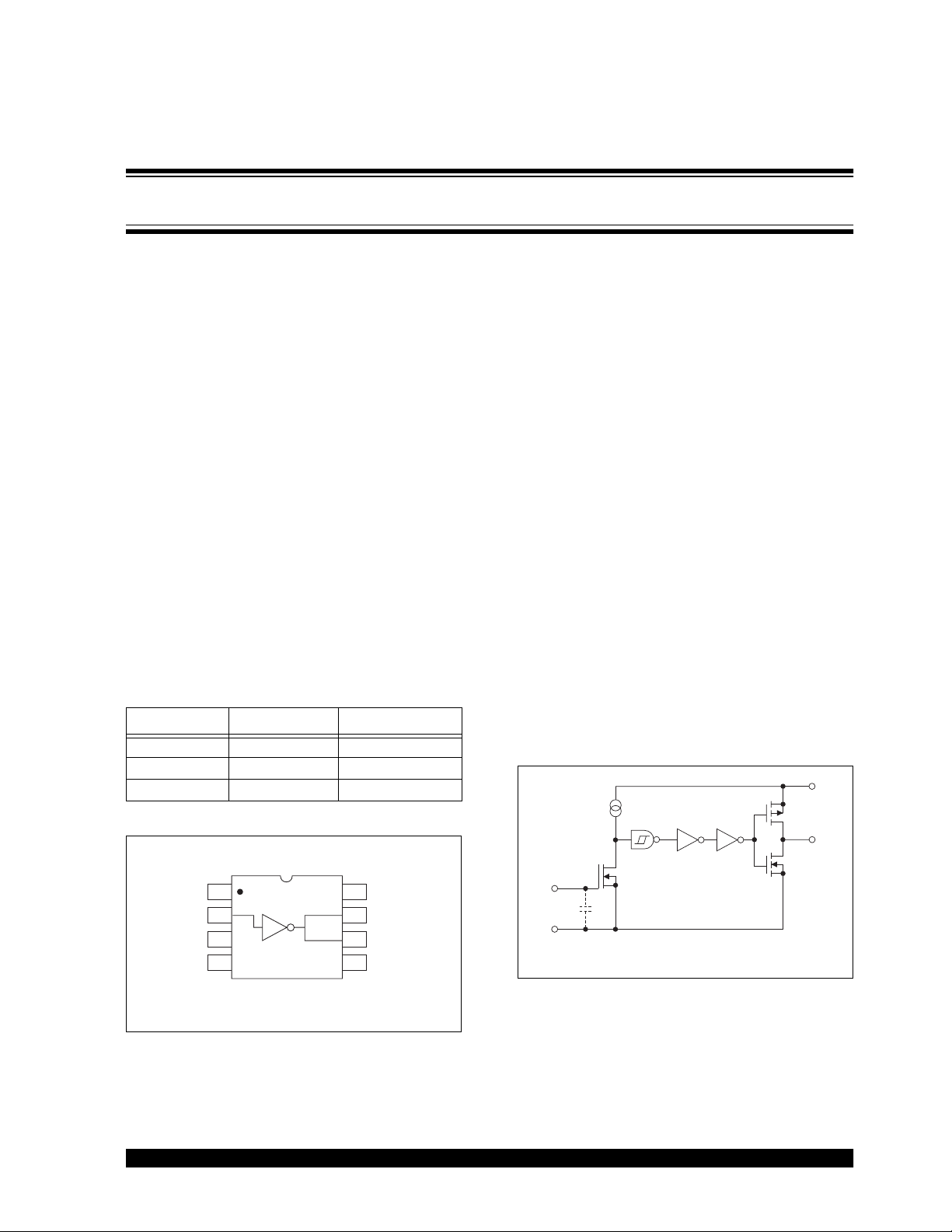
Typical Application
1,8
V
DD
Package Type
8-Pin PDIP/CERDIP
2
V
18
DD
27
INPUT
NC
36
45
NC = No internal connection
NOTE: Duplicate pins must both be connected for proper operation.
2002 Microchip Technology Inc. DS21416B-page 1
TC429
V
DD
OUTPUT
OUTPUT
GNDGND
Input
GND
4,5
Effective
Input
C = 38pF
300mV
TC429
6,7
Output
TC429
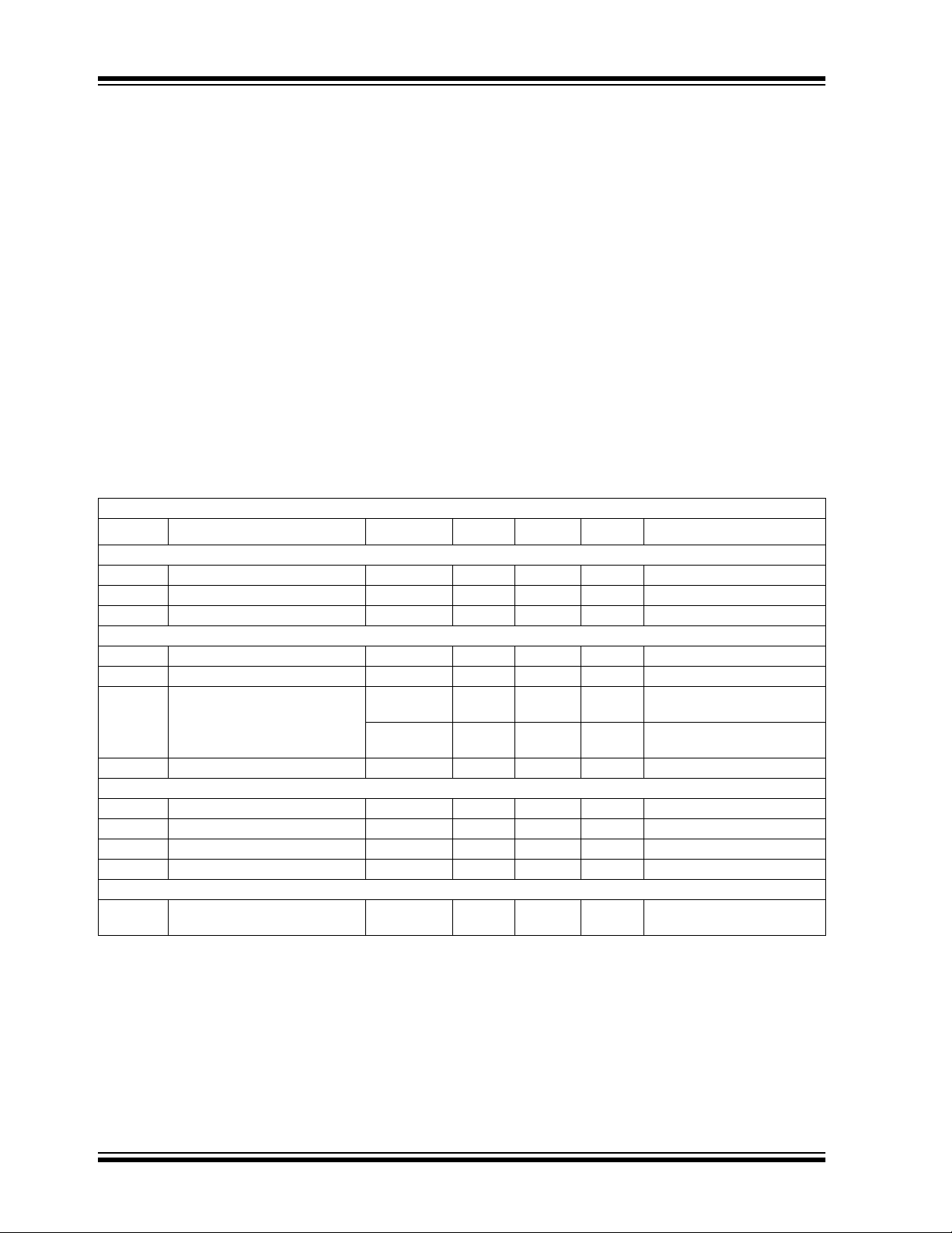
1.0 ELECTRICAL
CHARACTERISTICS
Absolute Maximum Ratings*
Supply Voltage.....................................................+20V
*Stresses above those listed under "Absolute Maximum
Ratings" may cause permanent damage to the device. These
are stress ratings only and functional operation of the device
at these or any other conditions above those indicated in the
operation sections of the specifications is not implied.
Exposure to Absolute Maximum Rating conditions for
extended periods may affect device reliability.
Input Voltage, Any Terminal
...................................V
+ 0.3V to GND – 0.3V
DD
Power Dissipation (TA ≤ 70°C)
PDIP.........................................................730mW
CERDIP....................................................800mW
Derating Factor
PDIP.................................5.6mW/°C Above 36°C
CERDIP................................................6.4mW/°C
Operating Temperature Range
C Version.........................................0°C to +70°C
E Version......................................-40°C to +85°C
M Ve rsion ...................................-55°C to +125°C
Storage Temperature Range..............-65°C to +150°C
TC429 ELECTRICAL SPECIFICATIONS
Electrical Characteristics: TA = +25°C with 7V ≤ V
Symbol Parameter Min Typ Max Units Test Conditions
Input
V
IH
V
IL
I
IN
Output
V
OH
V
OL
R
O
I
PK
Switching Time (Note 1)
t
R
t
F
t
D1
t
D2
Power Supply
I
S
Note 1: Switching times ensured by design.
Logic 1, High Input Voltage 2.4 1.8 — V
Logic 0, Low Input Voltage — 1.3 0.8 V
Input Curre n t -10 — 10 µA0V ≤ V
High Output Voltage VDD – 0.025 —— V
Low Output Voltage ——0.025 V
Output Resistance — 1.8 2.5 Ω VIN = 0.8V,
Peak Output Current — 6 — AVDD = 18V (Figure 3-4)
Rise Time — 23 35 nsec Figure 3-1, CL = 2500pF
Fall Time — 25 35 nsec Figure 3-1, CL = 2500pF
Delay Time — 53 75 nsec Figure 3-1
Delay Time — 60 75 nsec Figure 3-1
Power Supply Current —
≤ 18V, unless otherwise noted.
DD
— 1.5 2.5
3.5
—
0.3
0.5
≤ V
IN
DD
= 10mA, VDD = 18V
I
OUT
Ω V
5
mA VIN = 3V
= 2.4V,
IN
I
= 10mA, VDD = 18V
OUT
V
= 0V
IN
DS21416B-page 2 2002 Microchip Technology Inc.
TC429
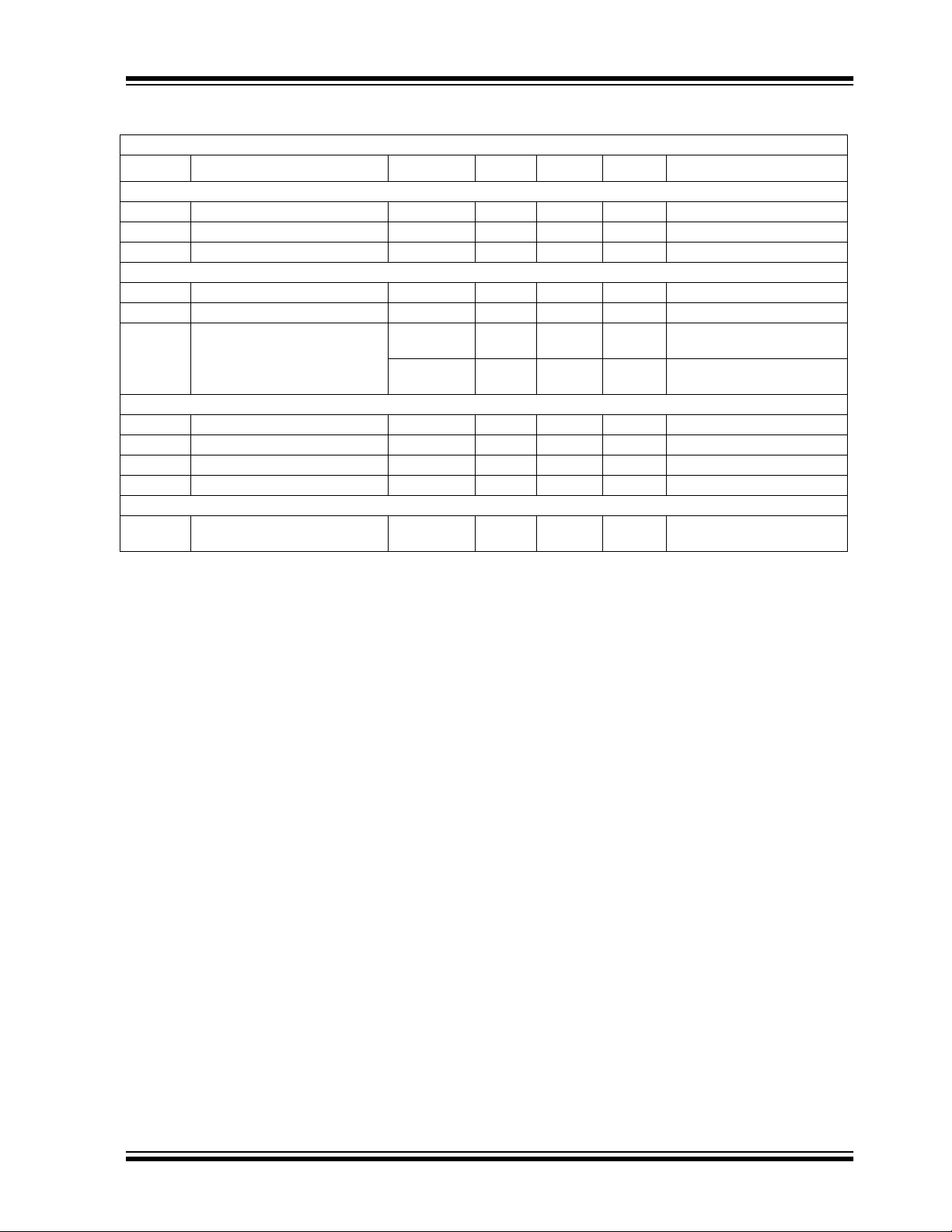
TC429 ELECTRICAL SPECIFICATIONS (CONTINUED)
Electrical Characteristics: Over operating temperature range with 7V ≤ V
Symbol Parameter Min Typ Max Units Test Conditions
Input
V
IH
V
IL
I
IN
Logic 1, High Input Voltage 2.4 —— V
Logic 0, Low Input Voltage ——0.8 V
Input Current -10 — 10 µA0V ≤ V
Output
V
OH
V
OL
R
O
High Output Voltage VDD – 0.025 ——V
Low Output Voltage ——0.025 V
Output Resistance ——5 Ω VIN = 0.8V,
——5
Switching Ti me (Note 1)
t
R
t
F
t
D1
t
D2
Rise Time ——70 nsec Figure 3-1, CL = 2500pF
Fall Time ——70 nsec Figure 3-1, CL = 2500pF
Delay Time ——100 nsec Figure 3-1
Delay Time ——120 nsec Figure 3-1
Power Supply
I
S
Note 1: Switching times ensured by design.
Power Supply Current —
—
—
—
≤ 18V, unless otherwise noted.
DD
I
OUT
12
Ω V
mA VIN = 3V
1
I
OUT
V
IN
IN
≤ V
IN
DD
= 10mA, VDD = 18V
= 2.4V,
= 10mA, VDD = 18V
= 0V
2002 Microchip Technology Inc. DS21416B-page 3
TC429
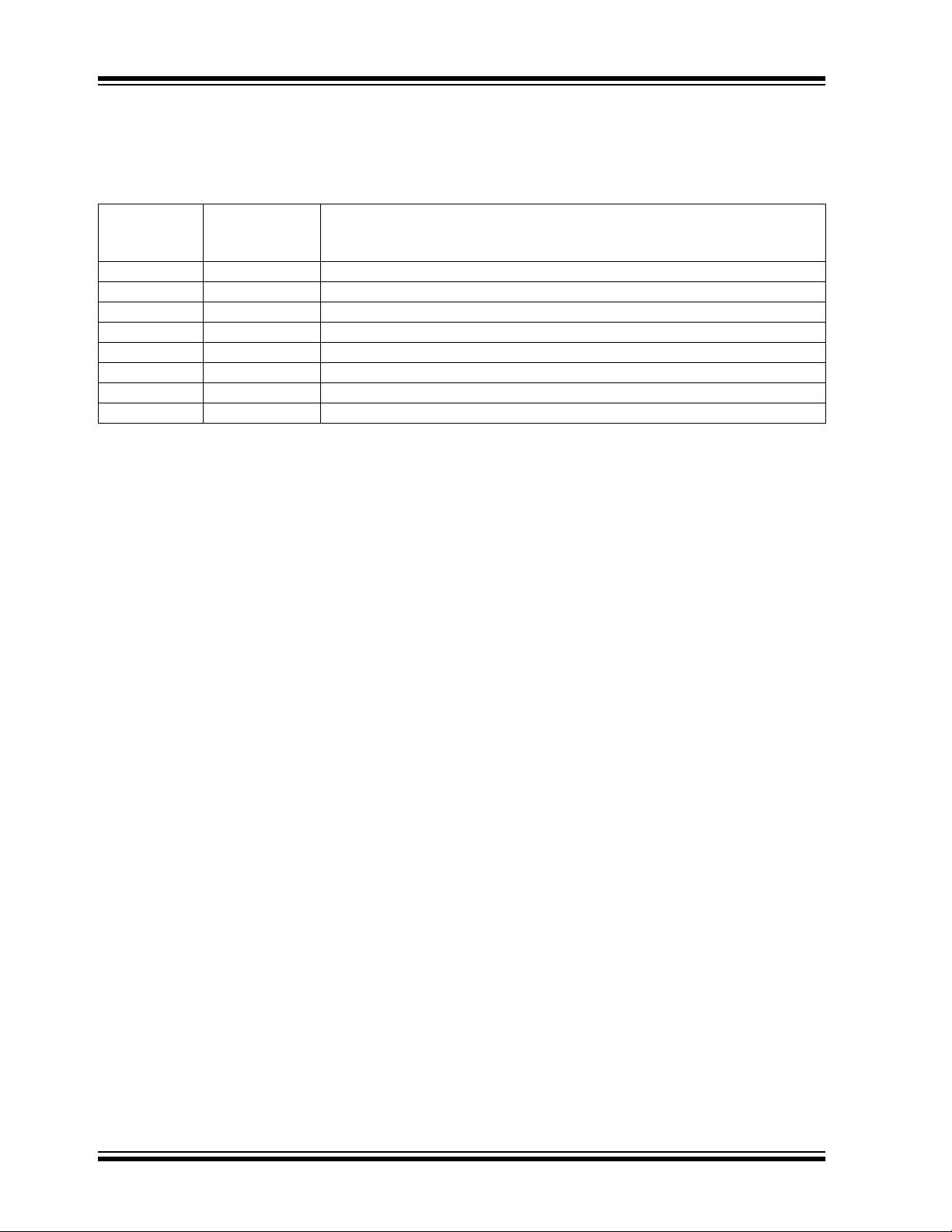
2.0 PIN DESCRIPTIONS
The descriptions of the pins are listed in Table 2-1.
TABLE 2-1: PIN FUNCTION TABLE
Pin No.
(8-Pin PDIP,
CERDIP)
1V
2 INPUT Control input, TTL/CMOS compatible logic input.
3 NC No connection.
4 GND Ground.
5 GND Ground.
6 OUTPUT CMOS totem-pole output, common to Pin 7.
7 OUTPUT CMOS totem-pole output, common to Pin 6.
8V
Symbol Description
DD
DD
Supply input, 7V to 18V.
Supply input, 7V to 18V.
DS21416B-page 4 2002 Microchip Technology Inc.
TC429
3.0 APPLICATIONS INFORMATION
3.1 Supply Bypassing
Charging and discharging large capacitive loads
quickly re qui res la rge cur rents . F or exam ple , ch argi ng
a 2500pF load to 18 V in 25nsec requires a 1.8A current
from the device’s power supply.
T o ensu re low supply im pedance over a wide frequency
range, a parallel capacitor combination is recommended for supply bypas sing. Low-induc tance ceramic
disk capacitors w ith short lead lengt hs (< 0.5 in.) shoul d
be used. A 1µF film c apac itor in p aral lel with o ne or tw o
0.1µF ceramic disk capacitors normally provides
adequate bypassing.
3.2 Grounding
The high-current capability of the TC429 demands
careful PC board layout for best performance. Since
the TC429 is an inverting driver, any ground lead
impedance will ap pear as negati ve feedback which can
degrade switching speed. The feedback is especially
noticeable with slow rise-time inputs, such as those
produced by an open-col lector outp ut with resis tor pullup. The TC429 input s tructure includes about 300mV of
hysteresis to ensure clean transitions and freedom
from oscillation, but attention to layout is still
recommended.
Figure 3-3 shows the feedback effect in detail. As the
TC429 input begins to go positive, the output goes
negative and several amperes of current flow in the
ground le ad. As l ittle as 0.05 Ω of PC trac e resistance
can produce hundre ds of millivolt s at the TC429 gro und
pins. If the driving logic is referenced to power ground,
the effective logi c input level is reduce d and oscillations
may result.
To ensure optimum device performance, separate
ground traces should be provided for the logic and
power connections. Con necting log ic ground di rectly to
the TC429 GND pins e nsures full logic d rive to the input
and fast output switching. Both GND pins should be
connected to power ground.
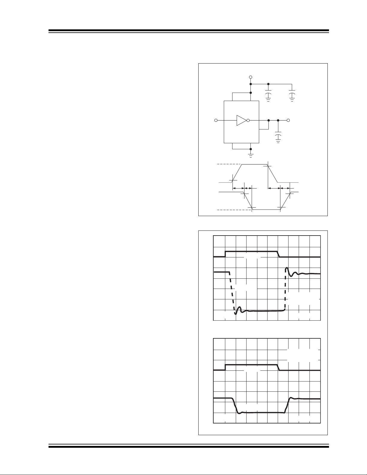
FIGURE 3-1: INVERTING DRIVER
SWITCHING TIME
TEST CIRCUIT
= 18V
V
DD
Output
CL = 2500pF
Input: 100kHz,
square wave,
t
= t
RISE
FALL
t
R
10%10%
0.1µF
18
26
Input
7
TC429
45
+5V
Input
10%
0V
18V
Output
0V
t
D1
90% 90%
t
F
t
1µF
90%
D2
FIGURE 3-2: SWITCHING SPEED
INPUT
OUTPUT
VOLTAGE (5V/DIV)
5V
TIME (100ns/DIV)
CL = 2500pF
V
= 18V
S
100ns
≤ 10nsec
CL = 2500pF
V
= 7V
S
INPUT
VOLTAGE (5V/DIV)
OUTPUT
5V
TIME (100ns/DIV)
2002 Microchip Technology Inc. DS21416B-page 5
100ns
 Loading...