

TC3405
T
16-Bit, Low Cost, Low Power Sigma-Delta A/D Converter
Features
• 16-bit Resolution at Eight Conversions Per
Second, Adjustable Down to 10-bit Resolution at
512 Conversions Per Second
• 1.8V – 5.5V Operation, Low Power Operating
250µA; Sleep: 35µA
• microPort™ Serial Bus Requires only two
Interface Lines
• Uses Internal or External Reference
• Automatically Enters Sleep Mode when not in use
• One Differential and Three Single-ended Inputs
with Built-In Multiplexer
•V
Monitor and Reset Generator Operational in
DD
Shutdown Mode
Applications
• Consumer Electronics, Thermostats, CO
Monitors, Humidity Meters, Security Sensors
• Embedded Systems, Data Loggers,
Portable Equipment
• Medical Instruments
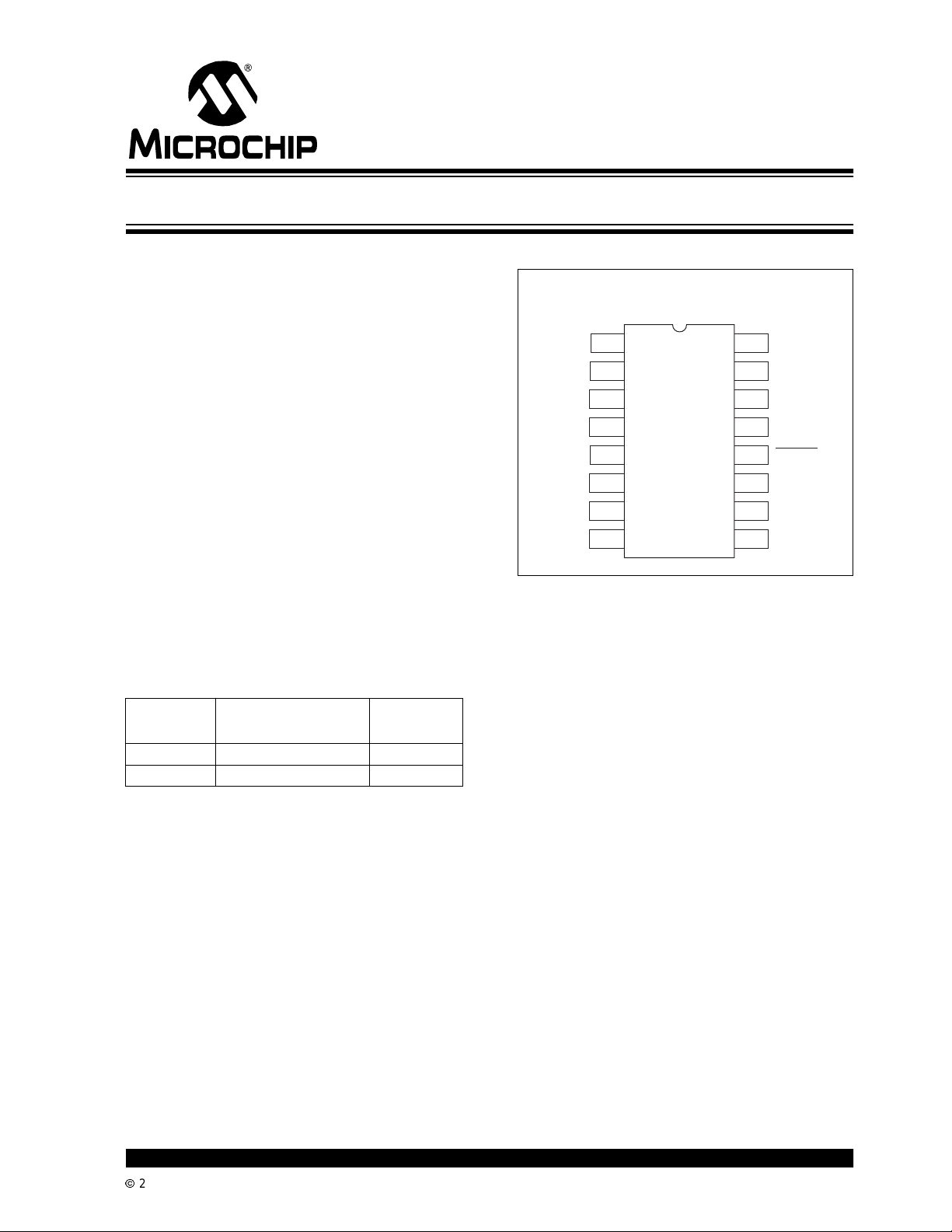
Device Selection Table
Part
Number
TC3405VPE 16-PinPDIP(Narrow) 0°Cto+85°C
TC3405VQR 16-PinQSOPNar row) 0°Cto+85°C
Package
Temperature
Range
Package Type
16-Pin PDIP
16-Pin QSOP
IN1+
V
REF
GND
1
215
IN1-
314
IN2
IN3
IN4
TH
IN
TC3405
413
512
611
710
89
16
V
DD
SCLK
A0
A1
RESET
ENABLE
SDAT
REF
OU
General Description
The TC3405 is a l ow cost, low power analog-to-digital
converter based on Microchip’s Sigma-Delta technology. I t will per form 16-bit conversions (15-bit pl us sign)
at up to eight per second. The TC3405 is optimized for
use as a microcontroller peripheral in low cost, battery
operated systems. A voltage reference is included, or
an external referencecan be used. A V
a resetgeneratorprovidesPower-on Reset and Brownout protection while an extra threshold detector is suitable for use as an early warning power fail detector,or
as a Wake-up Timer.
The TC3405’s 2-wire microPort™ digital interface is
used for starting conversions and for reading out the
data. Driving the SCLK line l ow starts a conversion.
Afterthe conversion starts, each additional falling edge
(up to six) detected on SCLK for t
the A/D resolution by one bit and cuts conversion time
in half. After a conversion is completed, clocking the
SCLK line puts the MSB t hrough LSB of the resulting
dataword onto the SDATline,much like a shift register.
The part automatically sleeps when not performing a
data conversion.
TheTC3405isavailableina16-PinPDIPanda16-Pin
QSOP package.
monitor with
DD
seconds reduces
4
2002 Microchip TechnologyInc. DS21414B-page 1
TC3405
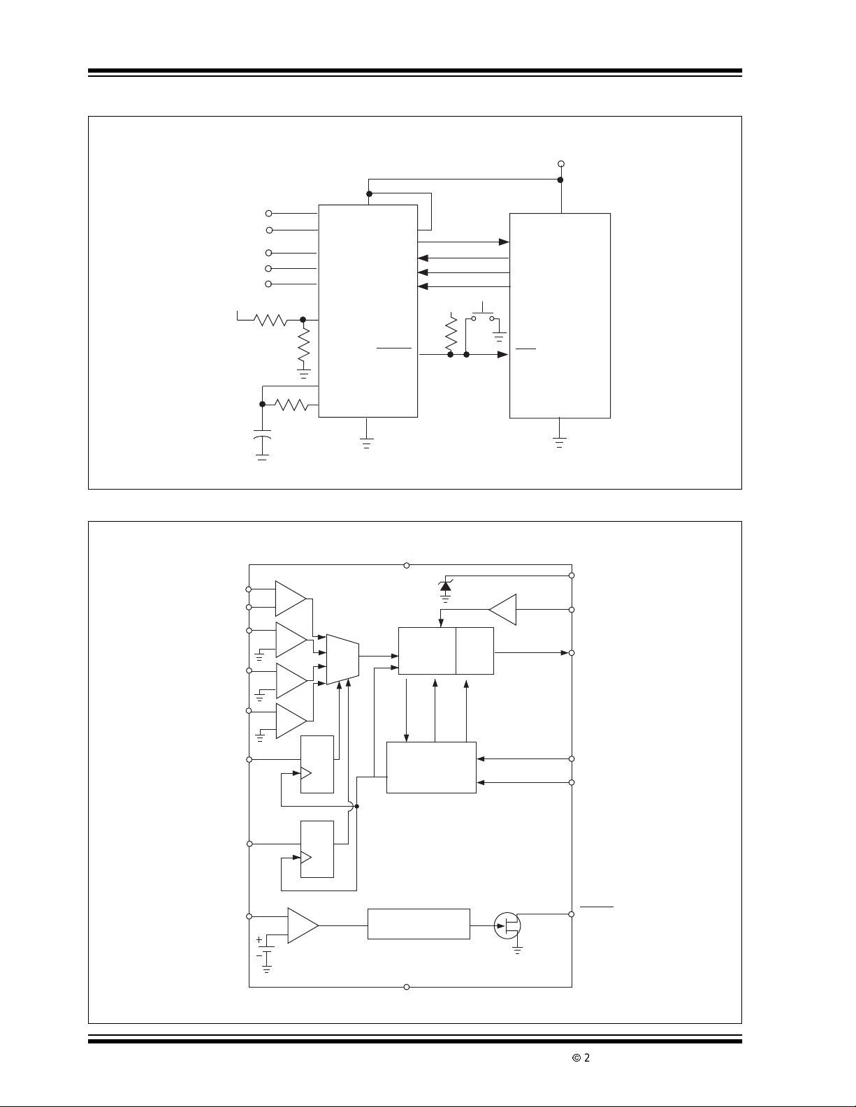
Typical Application
V
BATT
+
Input 1
–
+
Input 2
+
Input 3
Input 4 +
V
BATT
130kΩ
110kΩ
C1
0.1µF
Functional Block Diagram
IN1+
IN1-
IN2
IN3
IN4
A0
R1
R2
±10%
+
–
+
–
+
–
+
–
R3
390
IN1+
IN1-
IN2+
IN3+
IN4+
V
TH
REF
REF
1 of 4
AMux
SET
DQ
CLR
V
DD
ENABLE
TC3405
RESET
IN
OUT
TC3405
Start
Conv.
SDAT
SCLK
AO
AI
V
BATT
R6
100k
V
DD
Σ – ∆
Modulator
CONV done
CONVCLK
Clock Generator
and Control
Circuitry
1.193V
Data
Shift
Reg.
CLKOUT
x2
I/01
I/02
I/03
I/04
RST
V
CC
µ
Controller
REF
OUT
REF
IN
SDAT
SCLK
ENABLE
DS21414B-page 2
SET
A1
V
TH
–
+
1.23V
DQ
CLR
Reset Delay Timer
GND
RESET
2002 Microchip TechnologyInc.
TC3405
1.0 ELECTRICAL
CHARACTERISTICS
*Stresses above those listed under "Absolute Maximum
Ratings" may cause permanent damage to the device. These
are stress ratings only and functional operation of the device
at these or any other conditions above those indicated in the
Absolute Maximum Ratings*
Supply Voltage .....................................................6.0V
operation sections of the specifications is not implied.
Exposure to Absolute Maximum Rating conditions for
extended periods may affectdevice reliability.
Voltage on Pin:
RESET
................................ (GND – 0.3V) to 5.5V
Input Voltage (All Other Pins):
................................. (GND – 0.3V) to (V
DD
+0.3V)
Operating Temperature Range ................. 0°C to 85°C
Storage Temperature ........................ -65°C to +150°C
TC3405 DC ELECTRICAL SPECIFICATIONS
Electrical Characteristics: TA= 25°C and VDD= 2.7V, unless otherwise specified. Boldface type specifications apply for
temperaturesof 0°C to 85°C. V
Symbol Parameter Min Typ Max Unit Test Conditions
Power Supply
V
DD
I
DD
I
DDSLEEP
Supply Voltage 1.8 — 5.5 V
SupplyCurrent, DuringDataConversion — 250 — µA
Supply Current, Sleep Mode — 35 80 µATA=+25°C
Accuracy (Dif fere ntial Inputs)
RES Resolution — 16 — Bits
INL IntegralNon-Linearity — .0038 — %FSR V
V
OS
V
NOISE
Offset Error — — ±0.9 %FSR IN+, IN- = 0V
Referred to input — 60 — µVrms
CMR Common Mode Rejection — 75 — dB At DC
FSE Full Scale Error — 0.4% — %FS
PSRR Power SupplyRejection Ratio — 75 — dB V
INn+, INn-, INn
± Differential Input Voltage — — V
V
IN
Absolute Voltage RangeonINn+, INn-, INn GND — V
Input Bias Current — 1 100 nA
C
IN
R
IN
REF
V
REF
I
REF
V
REFOUT
REF
REF
Input Sampling Capacitance — 2 — pF
Differential Input Resistance — 2.0 — MΩ Note 2
REF
IN,
OUT
REFINVoltage Range 0 — 1.25 V
REFINInput Current — 1 — µA
SINK
SRC
REF
REF
REF
Voltage 1.175 1.193 — V
OUT
Current Sink Capability — 10 — µA
OUT
Current Source Capability 300 — — µA
OUT
Note 1: Differential input voltage defined as (V
2: Resistance from INn+ to INn- or INn to GND.
3: @V
=1.8V,I
DD
= 1.25V, Internal Clock Frequency = 520kHz.
REF
+–VIN-).
IN
≤ 200µA.
SOURCE
— 38 50
DD
DD
µA
DD
DD
V Note 1
V
=2.7V
=2.5Vto3.5V
2002 Microchip TechnologyInc. DS21414B-page 3
TC3405
TC3405 DC ELECTRICAL SPECIFICATIONS (CONTINUED)
Electrical Characteristics: TA= 25°C and VDD= 2.7V, unless otherwise specified. Boldface type specifications apply for
temperaturesof 0°C to 85°C. V
Symbol Parameter Min Typ Max Unit Test Conditions
SCLK, A0 A1, ENABLE
V
IL
V
IH
I
LEAK
Input Low Voltage — — 0.3 x
Input High Voltage 0.7xV
Leakage Current — 1 — µA
SDAT, RESET
V
OL
V
OH
V
DDMIN
V
TH
V
CCPFI
V
THR
,PFI
OutputLow Voltage — — 0.4 V IOL=1.5mA
OutputHighVoltage (SDAT) 0.9 x V
MinimumVDDfor PFO, RESET Valid — 1.1 1.3 µA
PFI Input VoltageRange 0 — V
, PFI Input Current -0.1 .01 0.1 µA
V
TH
Threshold (VTH,PFI) — 1.23 — V
Threshold Hysteresis — 30 — mV
Threshold Tempco — 30 — ppm/°C
Note 1: Differential input voltage defined as (V
2: Resistance from INn+ to INn- or INn to GND.
3: @V
=1.8V,I
DD
= 1.25V, Internal Clock Frequency = 520kHz.
REF
+–VIN-).
IN
≤ 200µA.
SOURCE
DD
DD
V
V
DD
——V
——VI
DD
SOURCE
V
=400µA (Note 3 )
TC3405 AC ELECTRICAL SPECIFICATIONS
Electrical Characteristics: T
temperaturesof 0°C to 85°C. V
Symbol Parameter Min Typ Max Unit Test Conditions
t
1
t
2
t
3
Resolution Reduction Clock Width 1 — — µsec Width of SCLK (Negative)
Resolution Reduction Clock Width 1 — — µsec Width of SCLK (Positive)
Conversion Time(15-bit Plus Sign) — 125 — msec 16-bit Conversion, TA=25°C(Note 1)
Conversion Time (14-bit Plus Sign) — t
Conversion Time (13-bit Plus Sign) — t
Conversion Time (12-bit Plus Sign) — t
Conversion Time(11-bit Plus Sign) — t
Conversion Time (10-bit Plus Sign) — t
Conversion Time(9-bitP lus Sign) — t
t
4
t
5
t
6
t
7
t
8
t
9
t
11
Resolution Reduction Window — t3/85.7 — msec Widthof SCLK
SCLK to Data Valid 1000 — — nsec SCLK FallingEdgeto SDAT Valid
Address Setup 0 — — nsec Address Valid to SCLK
Address Hold 1000 — — nsec SCLK to AddressValidHold
Acknowledge Delay — — 1000 nsec SCLKto SDAT Delay
RESET Active Time-out Period — t3*2 — msec Delay from POR or Brown-out
RESET Delay 5 — 64 µsec Delay VTHFalling at 10V/msec to
Note 1: Nominal temperature driftis -2830ppm/C° for temperature less than 25°C and -1340ppm/°C for temperatures
greater than 25°C
= 25°C and VDD= 2.7V, unless otherwise specified. Boldface type specifications apply for
A
= 1.25V, Internal Clock Frequency = 520kHz.
REF
/2.0 — msec 15-bit Conversion
3
/4.0 — msec 14-bit Conversion
3
/7.8 — msec 13-bit Conversion
3
/15.1 — msec 12-bitConversion
3
/28.6 — msec 11-bit Conversion
3
/51.4 — msec 10-bitConversion
3
Recovery to RESET
RESET
Low
=V
.
OH
DS21414B-page 4
2002 Microchip TechnologyInc.
TC3405
2.0 PIN DESCRIPTIONS
ThedescriptionsofthepinsarelistedinTable2-1.
TABLE 2-1: PIN FUNCTION TABLE
Pin No.
(16-Pin PDIP)
(16-Pin QSOP)
1 IN1+ AnalogInput. This is the positive terminalof a true differential input consisting of IN1+ and IN1-.
2 IN1- AnalogInput. This is the negative terminalof a true differential input consisting of IN1+ and IN1-.
3 IN2 Analog Input. This is the positive terminal of a true differential input with the negative input tied
4 IN3 Analog Input. This is the positive terminal of a true differential input with the negative input tied
5 IN4 Analog Input. This is the positive terminal of a true differential input with the negative input tied
6V
7REF
8 GND Ground Terminal.
9REF
10 SDAT Digital Output (push-pull). This is the microPort™ serial data output.S DAT is driven low while the
11 ENABLE Digital Input.Whenthisinput control is pulled low,t he partisinternally restarted.Thatis, any data
12 RESET
13 A1 DigitalInput. Controlsanalogmultiplexerinconjunction withA0 to select one of thefour input
14 A0 DigitalInput. Controlsanalogmultiplexerinconjunction withA1 to select one of thefour input
15 SCLK DigitalInput. This is the microPort™ serial clock input. The TC3405comes out of Sleep mode and a
16 V
Symbol Description
V
= (IN1+ – IN-). See Section 1.0, Electrical Characteristics.
IN1
= (IN+ – IN-) IN1- can swing to, but not below, ground. See Section 1.0, Electrical Characteristics.
V
IN1
internally to GND. See Section 1.0, Electrical Characteristics.
internally to GND. See Section 1.0, Electrical Characteristics.
internally to GND. See Section 1.0, Electrical Characteristics.
AnalogInput. This is the positive input to the internal comparator used to monitor the voltage supply.
TH
The negative input is tied to an internal reference. When V
reset generator drives RESET
AnalogInput. The converter’sreference voltageis the differentialbetween this pin and ground times
IN
two.ItmaybetieddirectlytoREF
reference voltage less than 1.25 may be used in place of REF
AnalogOutput. The internalreferenceconnects to this pin. It may be scaledexternally, and tiedto the
OUT
REF
inputto providetheconverter’s reference voltage.Caremustbe taken in connectingexternal
IN
circuitry to this pin. This pin is in a high impedance state during Sleep mode.
TC3405is converting data, effectively providing a “busy” signal. Afterthe conversion is complete,
every highto low transition on the SCLKpin putsa bit from the resulting data word on theSDAT pin
(from MSB to LSB).
conversion or data read sequence is cleared and the part goes into Sleep mode. When ENABLE
returns high, the part resumes normaloperation.
Digital Output(open drain).This is the outputoftheVDDmonitor reset generator. RESET is driven low
when a Power-on Reset or Brown-out condition is detected.
See Section 1.0, AC Electrical Characteristics.
channels. This address is latched at the falling edgeof the SCLK, which startsan A/D conversion.
A1, A0 = 00 = Input 1; 01 = Input 2; 10 = Input 3; 11 = Input 4.
channels. Thisaddress is latchedatthe fallingedgeofthe SCLK, whichstarts an A/Dconversion.A1,
A0=00=Input1;01=Input2;10=Input3;11=Input4.
conversion cycle begins when this pin is driven low. After the conversion starts, each additional
fallingedge(uptosix) detectedon SCLK for t
the conversion is complete, the data word can be shifted out on the S DAT pin by clocking the SCLK
pin.
Power SupplyInput.
DD
low. See Section 1.0, Electrical Characteristics.
or scaled using a resistor divider. Any user supplied
OUT
seconds, reduces the A/D resolution by one bit. When
4
falls belowtheinternal reference, the
TH
.
OUT
2002 Microchip TechnologyInc. DS21414B-page 5

TC3405
3.0 DETAILED DESCRIPTION
The TC3405 has a 16-bit sigma-delta A/D converter. It
has one differentialinput,three single-endedinputs,an
analog multiplexerand a V
ator. See the Typical Application circuit and the
Functional Block diagram. The key components of the
TC3405 are described below.
Alsoreferto Figure 3-5, A/D OperationalFlowchart and
the Timing Diagrams, Figure 3-1, Figure 3-2 and
Figure 3-3.
3.1 A/D Converter Operation
When the TC3405 is not converting, it is in Sleep mode
with both the SCLK and SDAT lines high. An A/D
conversionis initiated by a high to low transition on the
SCLK line at which time the internal clock of the
TC3405 is started and the address value (A0 and A1)
is internally latched. The addressvalue steers theanalog multiplexer to select the input channel to be
converted. Each additional high to low transition of
SCLK (following the initial SCLK falling edge) during
thetimeintervalt
resolutionbyonebit and reduce the conversion time by
one half. The time interval t
resolution reduction window. The minimum conversion
resolution is 10-bits so any more than 6 SCLK
transitionsduring t
After each high to low transition of SCLK, in the t
interval,the SDAT output is driven high by the TC3405
to acknowledge that the resolution has been decremented. W hen the SCLK returns hi gh or the t
ends,theSDAT line returnslow(seeFigure 3-2). When
the conversion is complete SDAT is driven high. The
TC3405 now enters Sleep mode and the conversion
value can be read as a serial data word on the SDAT
line.
4,
will be ignored.
4
monitorwith reset gener-
DD
will decrement the conversion
is referred to as the
4
interval
4
TABLE 3-1: DATA CONVERSION WORD
VS. VOLTAGE INPUT
(REF
Data Word INn+ –INn-(Volts)
0111 1111 1111 1111 2.38596 (PositiveFullScale)
0000 0000 0000 0001 72.8 E -6
0000 0000 0000 0000 0
1111 1111 1111 1111 -72.8 E -6
1000 0000 0000 0001 -2.38596 (Negative Full Scale)
1000 0000 0000 0000 Reserved Code
The SCLK i nput has a f ilter which r ejects any positive
or negative pulse of width less than 50nsec to reduce
noise. The rejection width of this pulse can vary
between 50nsec and 750nsec depending on processing parameters and supply voltage.
Figure 3-1 and Table3-2 show information for determining the mode of operation for the TC3401 part by
recording the value of SDAT for SCLK in a high, t hen
low, then high state. For example, if SCLK goes
through a 1-0-1 transition and the corresponding
values of SDAT are 1-1-0, then the SCLK falling edge
starteda new dataconversion.A 0-1-0 for SDAT would
have indicated a resolution reduction had occurred.
This i s useful if the microcontroller has a Watchdog
Reset or otherwise loses track of where the TC3405 is
in the conversion and data readout sequence. The
4
microcontroller can simply transition SCLK until it
“finds” a StartConversion condition.
= 1.193V)
IN
FIGURE 3-1: SCLK, SDAT LOGIC
STATE DIAGRAM
SCLK
3.2 Reading the Data Word
After the conversion is complete and SDAT goes high,
the conversion value can be clocked serially onto the
SDAT line by high to low transitions of the SCLK. The
datawordisintwo’scomplimentformat with the sign bit
clocked onto the SDAT line, first followed by the MSB
and ending in the LSB.For a 16-bit conversion the data
word would c onsist of a sign bit followed by 15 magnitude bits, Table 3-1 shows the data word versus input
voltage for a 16-bit conversion. Note that the full scale
input voltage range is ±(2 REF
REF
is fed back directly to REFIN,anLSBis73µV
OUT
for a 16-bit conversion, as REF
Figure 3-4 shows typical SCLK and SDAT waveforms
for 16, 12 and 10-bit conversions. Note that any completeconvert and read cycle requires17 negative edge
clock pulses. The first is the convert command. Then,
up to six of these can occur in the resolution reduction
window, t
, to decrement resolution. The remaining
4
pulses clock out the conversion data word.
DS21414B-page 6
– 1LSB). When
IN
is typically 1.193V.
OUT
SDAT
A
BC
TABLE 3-2: SCLK, SDAT LOGIC STATE
AB C Status
1 1 0 StartConversion
0 1 0 Resolution Reduction
x 1 1 Data Transfer
x 0 0 Data Transfer or Busy*
*Note: The code X00has a dualmeaning: DataTransferor
Busy converting. Toavoid confusion, the user should
send only the required number of pulses for the
desired resolution, then wait for SDAT to rise to 1,
indicating conversion is complete before clocking
SCLK againto read out data bits.
2002 Microchip TechnologyInc.

FIGURE 3-2: CONVERSION AND DATA OUTPUT TIMING
t
2
t
SCLK
SDAT
1
t
t
4
t
3
t
8
8
D
N
(MSB)
Data Conversion
Complete
t6t
7
A0, A1
Start Conversion and Resolution Control Timing Data Output Timing
FIGURE 3-3: RESET AND POWER FAIL TIMING
TC3405
t
5
D
N-1
D
N-1
D
0
(LSB)
Sleep
Mode
1.80
1.23
1.20
1.1
0
RESET
Volts
Hysteresis
V
DD
V
TH
Time
t
9
Reset Generator Timing
V
DD
t
t
9
11
t
11
2002 Microchip TechnologyInc. DS21414B-page 7

TC3405
FIGURE 3-4: SCLK AND SDAT WAVEFORMS FOR 16, 12 AND 10-BIT CONVERSIONS
16-bit Data Conversion,
SCLK
t3a
SDAT
Data Conversion
Complete
Data Word A5A5h
SCLK
SDAT
SCLK
SDAT
SCLK
SDAT
> t3a
Data Conversion
Complete
< t
4
t3e
< t
4
t3g
16-bit Data Conversion, Long Start Pulse,
Data Word 5A5Ah
12-bit Conversion,
Data Word = AB3h
Data Conversion
Complete
10-bit Conversion with "Extra"
Data Reduction Clocks, Data Word = 3A4h
DS21414B-page 8
Data Conversion
Complete
2002 Microchip TechnologyInc.

FIGURE 3-5: A/D OPERATIONAL FLOWCHART
TC3405
POR
Sleep
SDAT = High
No
Channel Address (if applicable).
SCLK
Hgh to Low?
Yes
Power Up Analog,
Start CONVCLK (= 0),
Start Conversion,
Resolution = 2m
(m = 16), Latch Input
SCLK
Low to High
transition?
Yes
No
SDAT = Low
CONVCLK = 2m?
(Conversion Done?)
Yes
Power Down Analog,
Conversion Complete,
SDAT = High
SCLK
High to Low?
Yes
SDAT = Dm;
m = m – 1
No
No
SDAT = Low
CONVCLK
No
No
SCLK
High to Low?
Resolution
> 2
Reduce A/D
Resolution by 1-bit
(m = m – 1);
SDAT = High
< 2
A/D
9
10
?
Yes
Yes
?
Yes
No
m ≥ 0?
No
SDAT = High
Internal Reset
Sleep
Yes
2002 Microchip TechnologyInc. DS21414B-page 9

TC3405
3.3 VDDMonitor
The TC3405 RESET output is in high impedance
provided the voltage at V
voltage reference. This reference is approximately the
samevalue as the voltage appearingat REF
V
is lessthan the internalreference,RESETispulled
TH
low. When V
rises above the internal reference
TH
voltage again, RESET
time-out period, t
, before being released. The RESET
9
output is valid for VDD=1.3Vto5.5V.
When used to generate a Power-on or Brown-out
Reset,an external resistor network is required to divide
the appropriate V
V
input, (See the Typical Application circuit). For
TH
DD
example, to generate a POR for a V
values of R1 and R2 should be 137kΩ and 115kΩ
respectively.
Since RESET
is an open drain, it can be wired-OR’ed
with another open drain or external switch if desired.
is greater than the internal
TH
.When
OUT
is held low for the reset active
threshold down to 1.23V at the
at 3V -10%, the
DD
DS21414B-page 10
2002 Microchip TechnologyInc.

4.0 PACKAGING INFORMATION
4.1 Package Marking Information
Package marking data not available at this time.
4.2 Taping Forms
Component Taping Orientation for 16-Pin QSOP (Narrow) Devices
PIN 1
TC3405
User Direction of Feed
W
P
Standard Reel Component Orientation
for TR Suffix Device
Carrier Tape, Reel Size, Number of Components Per Reel and Reel Size
Package Carrier Width (W) Pitch (P) Part Per Full Reel Reel Size
16-Pin QSOP (N) 12 mm 8 mm 2500 13 in
2002 Microchip TechnologyInc. DS21414B-page 11

TC3405
)
4.3 Package Dimensions
16-Pin PDIP (Narrow)
.045 (1.14)
.030 (0.76)
.200 (5.08)
.140 (3.56)
.150 (3.81)
.115 (2.92)
.770 (19.56)
.740 (18.80)
PIN 1
.270 (6.86)
.240 (6.10)
.040 (1.02)
.020 (0.51)
.014 (0.36)
.008 (0.20)
.310 (7.87)
.290 (7.37)
10°
MAX.
.110 (2.79)
.090 (2.29)
.070 (1.78)
.045 (1.14)
16-Pin QSOP (Narrow)
PIN 1
.157 (3.99)
.150 (3.81)
.010 (0.25)
.004 (0.10)
.025
(0.635)
TYP.
.196 (4.98)
.189 (4.80)
.012 (0.31)
.008 (0.21)
.022 (0.56)
.015 (0.38)
.244 (6.20)
.228 (5.80)
.069 (1.75)
.053 (1.35)
8°
MAX.
.400 (10.16)
.310 (7.87)
Dimensions: inches (mm
.010 (0.25)
.007 (0.19)
.050 (1.27)
.016 (0.41)
Dimensions: inches (mm)
DS21414B-page 12
2002 Microchip TechnologyInc.

TC3405
SALES AND SUPPORT
Data Sheets
Products supportedby a preliminaryData Sheet may have an errata sheet describing minor operational differences and recommendedworkarounds.To determine if an erratasheetexists for a particular device,please contact one of the following:
1. Y our local Microchip sales office
2. The MicrochipCorporate Literature Center U.S. FAX: (480) 792-7277
3. The Microchip Worldwide Site (www.microchip.com)
Pleasespecify which device, revision of silicon and Data Sheet (includeLiterature #) you are using.
New Customer Notification System
Register on our web site (www.microchip.com/cn) to receive the mostcurrenti nformationon our products.
© 2002 Microchip TechnologyInc. DS21414B-page13

TC3405
NOTES:
DS21414B-page 14 © 2002 Microchip TechnologyInc.

TC3405
Information contained in this publication regarding device
applications and the like is intended through suggestion only
and may be superseded by updates. It is your responsibility to
ensure that your application meets with your specifications.
No representation or warranty is given and no liability is
assumed by Microchip Technology Incorporated with respect
to the accuracy or use of such information,or infringement of
patents or other intellectual property rights arising from such
use or otherwise. Use of Microchip’s products as critical components in life support systems is not authorized except with
express written approval by Microchip. No licenses are conveyed, implicitly or otherwise, under any intellectual property
rights.
Trademarks
The Microchip name and logo, the Microchip logo, FilterLab,
K
EELOQ,microID,MPLAB,PIC,PICmicro,PICMASTER,
PICSTART, PRO MATE, SEEVAL and The Embedded Control
SolutionsCompany areregiste red trademarksof MicrochipTechnologyIncorp or ated in the U.S.A. and other countries .
dsPIC, ECONOMONITOR, Fa nSense, FlexROM, fuzzyLAB,
In-Circuit Serial Programming, ICSP, ICEPIC, microPort,
Migratable Memory, MPASM, MPLIB, MPLINK, MPSIM,
MXDEV, PICC, PICDEM, PICDEM.net , rfPIC, Select Mode
and TotalEndurancearetrademarksofMicrochipTechnology
Incorporated in the U.S.A.
Serialized Quick Turn Programming (SQTP) is a service mark
of Microchip TechnologyIncorporated in t he U.S.A.
All other trademarks mentioned herein are property of their
respective companies.
© 2002, Microchip Technology Incorporated, Printed in the
U.S.A., All Rights Reserved.
Printed on recycled paper.
Microchip received QS-9000 quality system
certification for its worldwide headquarters,
design and wafer fabrication facilities in
Chandler and Tempe, Arizona in July 1999
and Mountain View, California in March 2002.
The Company’s quality system processes and
procedures are QS-9000 compliant for its
®
PICmicro
devices, Serial EEPROMs, microperipherals,
non-volatile memory and analog products. In
addition, Microchip’s quality system for the
design and manufacture of development
systemsisISO 9001certified.
2002 Microchip TechnologyInc. DS21414B-page 15
8-bit MCUs, KEELOQ®code hopping

WORLDWIDE SALES AND SERVICE
AMERICAS
Corporate Office
2355 West Chandler Blvd.
Chandler, AZ 85224-6199
Tel: 480-792-7200 Fax: 480-792-7277
Technical Support: 480-792-7627
Web Address: http://www.microchip.com
Rocky Mountain
2355 West Chandler Blvd.
Chandler, AZ 85224-6199
Tel: 480-792-7966 Fax: 480-792-7456
Atlanta
500 Sugar Mill Road, Suite 200B
Atlanta, GA 30350
Tel: 770-640-0034 Fax: 770-640-0307
Boston
2 Lan Drive, Suite 120
Westford, MA 01886
Tel: 978-692-3848 Fax: 978-692-3821
Chicago
333 Pierce Road, Suite 180
Itasca, IL 60143
Tel: 630-285-0071 Fax: 630-285-0075
Dallas
4570 Westgrove Drive, Suite 160
Addison, TX 75001
Tel: 972-818-7423 Fax: 972-818-2924
Detroit
Tri-Atria Office Building
32255 Northwestern Highway, Suite 190
Farmington Hills, MI 48334
Tel: 248-538-2250 Fax: 248-538-2260
Kokomo
2767 S. Albright Road
Kokomo, Indiana 46902
Tel: 765-864-8360 Fax: 765-864-8387
Los Angeles
18201 Von Karman, Suite 1090
Irvine, CA 92612
Tel: 949-263-1888 Fax: 949-263-1338
New York
150 Motor Parkway, Suite 202
Hauppauge, NY 11788
Tel: 631-273-5305 Fax: 631-273-5335
San Jose
Microchip Technology Inc.
2107 North First Street, Suite 590
San Jose, CA 95131
Tel: 408-436-7950 Fax: 408-436-7955
Toronto
6285 Northam Drive, Suite 108
Mississauga, Ontario L4V 1X5, Canada
Tel: 905-673-0699 Fax: 905-673-6509
ASIA/PACIFIC
Australia
Microchip Technology Australia Pty Ltd
Suite 22, 41 Rawson Street
Epping 2121, NSW
Australia
Tel: 61-2-9868-6733 Fax: 61-2-9868-6755
China - Beijing
Microchip T echnology Consulting (Shanghai)
Co., Ltd., Beijing Liaison Office
Unit 915
Bei Hai Wan Tai Bldg.
No. 6 Chaoyangmen Beidajie
Beijing, 100027, No. China
Tel: 86-10-85282100 Fax: 86-10-85282104
China - Chengdu
Microchip T echnology Consulting (Shanghai)
Co., Ltd., Chengdu Liaison Office
Rm. 2401, 24th Floor,
Ming Xing Financial Tower
No. 88 TIDU Street
Chengdu 610016, China
Tel: 86-28-86766200 Fax: 86-28-86766599
China - Fuzhou
Microchip T echnology Consulting (Shanghai)
Co., Ltd., Fuzhou Liaison Office
Unit 28F, World Trade Plaza
No. 71 Wusi Road
Fuzhou 350001, China
Tel: 86-591-7503506 Fax: 86-591-7503521
China - Shanghai
Microchip T echnology Consulting (Shanghai)
Co., Ltd.
Room 701, Bldg. B
Far East International Plaza
No. 317 Xian Xia Road
Shanghai, 200051
Tel: 86-21-6275-5700 Fax: 86-21-6275-5060
China - Shenzhen
Microchip T echnology Consulting (Shanghai)
Co., Ltd., Shenzhen Liaison Office
Rm. 1315, 13/F , Shenzhen Kerry Centre,
Renminnan Lu
Shenzhen 518001, China
Tel: 86-755-2350361 Fax: 86-755-2366086
China - Hong Kong SAR
Microchip Technology Hongkong Ltd.
Unit 901-6, Tower 2, Metroplaza
223 Hing Fong Road
Kwai Fong, N.T., Hong Kong
Tel: 852-2401-1200 Fax: 852-2401-3431
India
Microchip Technology Inc.
India Liaison Office
Divyasree Chambers
1 Floor, Wing A (A3/A4)
No. 11, O’Shaugnessey Road
Bangalore, 560 025, India
Tel: 91-80-2290061 Fax: 91-80-2290062
Japan
Microchip Technology Japan K.K.
Benex S-1 6F
3-18-20, Shinyokohama
Kohoku-Ku, Yokohama-shi
Kanagawa, 222-0033, Japan
Tel: 81-45-471- 6166 Fax: 81-45-471-6122
Korea
Microchip Technology Korea
168-1, Youngbo Bldg. 3 Floor
Samsung-Dong, Kangnam-Ku
Seoul, Korea 135-882
Tel: 82-2-554-7200 Fax: 82-2-558-5934
Singapore
Microchip Technology Singapore Pte Ltd.
200 Middle Road
#07-02 Prime Centre
Singapore, 188980
Tel: 65-6334-8870 Fax: 65-6334-8850
Taiwan
Microchip Technology Taiwan
11F-3, No. 207
Tung HuaNorth Road
Taipei, 105, Taiwan
Tel: 886-2-2717-7175 Fax: 886-2-2545-0139
EUROPE
Denmark
Microchip Technology Nordic ApS
Regus Business Centre
Lautrup hoj 1-3
Ballerup DK-2750 Denmark
Tel: 45 4420 9895 Fax: 45 4420 9910
France
Microchip Technology SARL
Parc d’Activite du Moulin de Massy
43 Rue du Saule Trapu
Batiment A - ler Etage
91300 Massy, France
Tel: 33-1-69-53-63-20 Fax: 33-1-69-30-90-79
Germany
Microchip Technology GmbH
Gustav-Heinemann Ring 125
D-81739 Munich, Germany
Tel: 49-89-627-144 0 Fax: 49-89-627-144-44
Italy
Microchip Technology SRL
Centro Direzionale Colleoni
Palazzo Taurus 1 V. Le Colleoni 1
20041 Agrate Brianza
Milan, Italy
Tel: 39-039-65791-1 Fax: 39-039-6899883
United Kingdom
Microchip Ltd.
505 Eskdale Road
Winnersh Triangle
Wokingham
Berkshire, EnglandRG41 5TU
Tel: 44 118 921 5869 Fax: 44-118 921-5820
05/01/02
DS21414B-page 16
*DS21414B*
2002 Microchip Technology Inc.
 Loading...