

DUAL RS-232 TRANSMITTER/RECEIVER AND POWER SUPPLY
TC232*
*Patented
FEATURES
■ Meets All RS-232 Specifications
■ Operates From Single 5V Power Supply
■ 2 Drivers and 2 Receivers
■ On-Board Voltage Quadrupler
■ Input Levels.......................................................±30V
■ Output Swing With +5V Supply .........................±9V
■ Low Supply Current ........................................ 5 mA
■ Does not require external ±12V supplies
APPLICATIONS
■ RS-232C Communication Links
■ Modems, peripherals, computers
■ Battery-powered systems
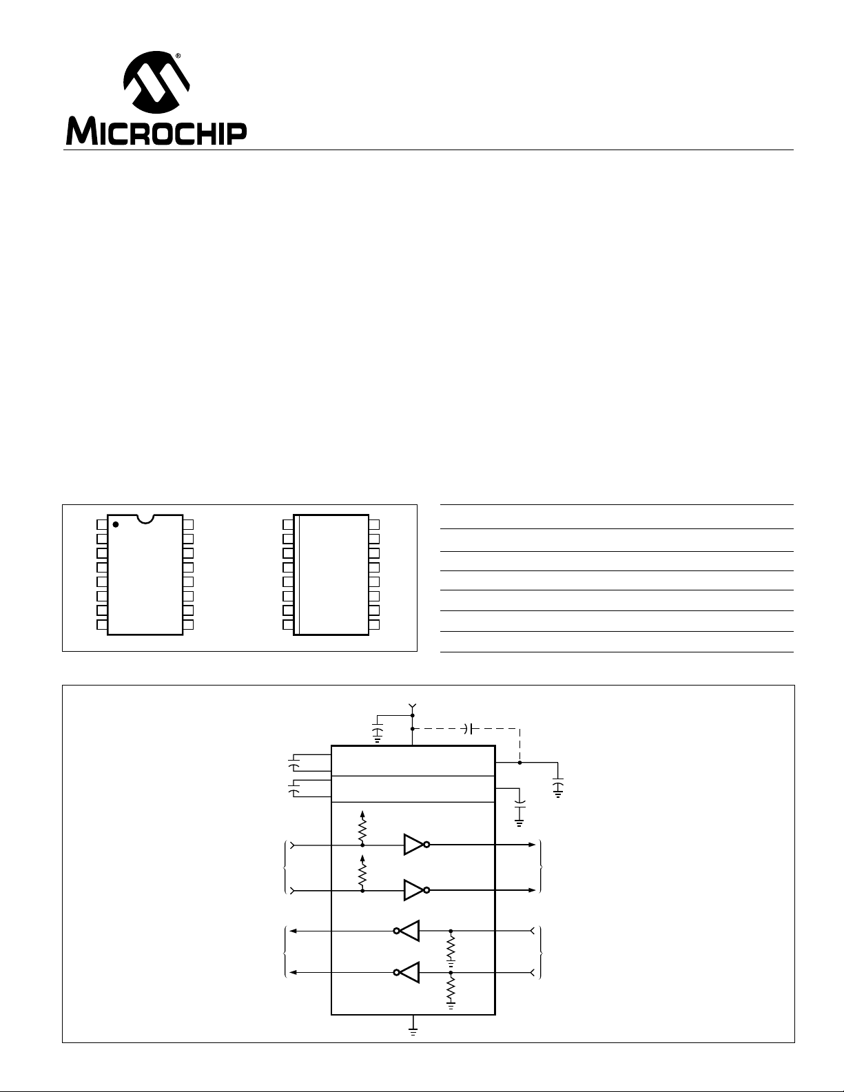
PIN CONFIGURATIONS (DIP and SOIC)
+
C
1
1
+
2
V
–
C
3
1
+
C
4
2
–
C
V
T2
OUT
R2
TC232CPE
5
2
TC232EPE
–
6
TC232IJE
TC232MJE
7
8
IN
16
V
CC
GND
15
14
T1
OUT
R1
13
IN
12
R1
OUT
T1
11
IN
T2
10
IN
9
R2
OUT
+
C
1
1
+
2
V
–
C
3
1
+
C
4
2
–
C
TC232COE
5
2
TC232EOE
–
V
6
T2
7
OUT
R2
8
IN
16
V
CC
GND
15
14
T1
OUT
R1
13
IN
12
R1
OUT
T1
11
IN
T2
10
IN
9
R2
OUT
GENERAL DESCRIPTION
The TC232 is a dual RS-232 transmitter/receiver that
complies with EIA /TIA RS-232E guidelines and is ideal for
all RS-232 communication links. This device operates from
a 5V power supply and contains two charge pump voltage
converters that produce ±10V power supplies.
The TC232 has four level translators. Two are RS-232
transmitters that convert TTL/CMOS input levels to 9V
RS-232 outputs. The other two translators are RS-232
receivers that convert RS-232 inputs to 5V TTL/CMOS
output levels. The receivers have a nominal threshold of
1.3V, a typical hysteresis of 0.5V, and can operate with
inputs up to ±30V.
ORDERING INFORMATION
Part No. Package Temp. Range
TC232COE 16-Pin SOIC (Wide) 0°C to +70°C
TC232CPE 16-Pin Plastic DIP 0°C to +70°C
TC232EOE 16-Pin SOIC (Wide) – 40°C to +85°C
TC232EPE 16-Pin Plastic DIP – 40°C to +85°C
TC232IJE 16-Pin CerDIP – 25°C to +85°C
TC232MJE 16-Pin CerDIP – 55°C to +125°C
TYPICAL APPLICATION
C3 can be connected between
*NOTE:
V+ and VCC for convenience.
© 2001 Microchip Technology Inc. DS21396A
TTL/CMOS
INPUTS
TTL/CMOS
OUTPUTS
10 µF
10 µF
+5V INPUT
+
10 µF
1
+
+
C1
+
C2
C
1
3
–
C
1
4
+
C
2
5
–
C
2
+5V
400 kΩ
T1
11
IN
+5V
400 kΩ
T2
10
IN
R1
12
OUT
R2
9
OUT
16
V
CC
+5V TO +10V
VOLTAGE DOUBLER
+10V TO –10V
VOLTAGE INVERTER
T1
T2
R1
R2
GND
15
C3*
10 µF
5 kΩ
+
2
+
V
+10V
–10V
–
V
6
T1
14
OUT
T2
7
OUT
R1
13
IN
R2
8
IN
Ω5 k
+
C4
10 µF
+
C3*
10 µF
RS-232
OUTPUTS
RS-232
INPUTS
TC232-6 10/21/96
TC232
DUAL RS-232 TRANSMITTER/
RECEIVER AND POWER SUPPLY
ABSOLUTE MAXIMUM RATINGS*
Package Power Dissipation (TA ≤ 70°C)
CerDIP............................................................890mW
VCC............................................................................. +6V
V+........................................................................... +12V
V–........................................................................... +12V
Input Voltages
T1IN, T2IN....................................–0.3 to (VCC +0.3V)
Derate 9.5 mW/°C Above +70°C
Plastic DIP ......................................................840mW
Derate 7 mW/°C Above +70°C
Small Outline (SOIC) ......................................760mW
Derate 7 mW/°C Above +70°C
R1IN, R2IN......................................................... ±30V
Output Voltages
T1
R1
OUT
OUT
, T2
, R2
...................... (V+ +0.3V) to (V– –0.3V)
OUT
..............................–0.3 to (VCC +0.3V)
OUT
Short Circuit Duration
V+.................................................................... 30sec
V–.................................................................... 30sec
T1
OUT
, T2
..........................................Continuous
OUT
*Static-sensitive device. Unused devices must be stored in conductive
material. Protect devices from static discharge and static fields.
Stresses above those listed under "Absolute Maximum Ratings" may
cause permanent damage to the device. These are stress ratings only
and functional operation of the device at these or any other conditions
above those indicated in the operation sections of the specifications is
not implied. Exposure to absolute maximum rating conditions for
extended periods may affect device reliability.
Storage Temperature Range .................. -65°C to +150°C
ELECTRICAL CHARACTERISTICS: V
= 5V ±10%, TA = operating temperature range, test circuit unless
CC
otherwise noted.
Parameter Test Conditions Min Typ Max Unit
Output Voltage Swing T1
Power Supply Current — 5 10 mA
Input Logic Threshold Low T1IN, T2
Input Logic Threshold High T1IN, T2
Logic Pull-Up Current T1IN, T2IN = 0V — 15 200 µA
RS-232 Input Voltage Operating Range – 30 — +30 V
RS-232 Input Threshold Low VCC = 5V 0.8 1.2 — V
RS-232 Input Threshold High VCC = 5V — 1.7 2.4 V
RS-232 Input Hysteresis 0.2 0.5 1 V
RS-232 Input Resistance TA = +25°C, VCC = 5V 3 5 7 kΩ
TTL/CMOS Output Voltage Low I
TTL/CMOS Output Voltage High I
Propagation Delay RS-232 to TTL or TTL to RS-232 — 0.5 — µsec
Instantaneous Slew Rate CL = 10 pF, RL = 3 kΩ to 7 kΩ,——30V/µsec
Transition Region Slew Rate RL = 3 kΩ, CL = 2500 pF — 3 — V/µsec
Output Resistance VCC = V+ = V– = 0V, V
RS-232 Output — ±10 — mA
Short-Circuit Current
NOTE 1. Sample tested.
, T2
OUT
3 kΩ to Ground
= 3.2 mA — — 0.4 V
OUT
= – 1 mA 3.5 — — V
OUT
TA = +25°C (Note 1)
Measured From +3V to – 3V
or –3V to +3V
Loaded With ±5 ±9 ±10 V
OUT
IN
IN
= ±2V 300 — — Ω
OUT
— — 0.8 V
2——V
TC232-6 10/21/96
2
© 2001 Microchip Technology Inc. DS21396A

DUAL RS-232 TRANSMITTER/
RECEIVER AND POWER SUPPLY
TC232
DETAILED DESCRIPTION
The TC232 contains a +5V to ±10V dual charge pump
voltage converter, a dual transmitter and a dual receiver.
+5V to ±10V Dual Charge Pump
Voltage Converter
The TC232 power supply consists of two charge pumps.
One uses external capacitor C1 to double the +5V input to
+10V, with output impedance of about 200Ω. The other
uses C2 to invert +10V to – 10V, with overall output
impedance of 450Ω (including effects of +5V to +10V
doubler impedance).
The clock in the doubler circuit will start at ≈4.2V in the
typical part, but external loads may make this point rise to as
high as 4.5V with a load of 2 kΩ on each of the two output
voltages.
Because of this, use of the doubler and inverter to run
additional external circuits should be limited. The maximum
current should be no more than 2.5 mA from the +10V and
- 10V. in order to guarantee start-up of the doubler clock.
The test circuit employs 22 µF capacitors for C1 to C4,
but the value is not critical. These capacitors usually are lowcost aluminum or tantalum electrolytic capacitors.
Increasing C1 and C2 to 47 µF lowers the output
impedance of the +10V doubler and the - 10V inverter by
the change in the ESR of the capacitors.
Increasing C3 and C4 lowers ripple on the ±10V outputs and 16 kHz ripple on the RS-232 outputs. Where size
is critical, the value of C1 to C4 can be lowered to 1 µF. The
use of a low ESR capacitor will help lower the output ripple
and keep the output impedance of the ±10V as low as
possible.
V+, V– Output Voltages vs. Load Current
10
9
8
7
–
V
(V = 4.5V)
CC
6
5
CONDITIONS:
OUTPUT VOLTAGE (|V|)
A) T = +25°C
A
4
B) TRANSMITTER OUTPUTS
OPEN CIRCUIT
3
0 12345678910
+
V
(V = 4.5V)
CC
| I | (mA)
LOAD
+
V
(V = 5V)
CC
–
V
(V = 5V)
CC
The outputs are protected and can be short-circuited to
ground indefinitely.
Dual Receiver
TC232 receivers meet RS-232 input specifications.
Input impedance is between 3 kΩ and 7 kΩ. Switching
thresholds are within the ±3V limits, and the receivers
withstand up to ±30V inputs. RS-232 and TTL/CMOS input
compatible, the receivers have 0.8V VIL and 2.4V VIH with
0.5V hysteresis to reject noise.
The TTL/CMOS compatible receiver output is LOW
when an RS-232 input is greater than 2.4V. It is HIGH
when an input is floating or between +0.8V and – 30V.
Dual Transmitter
TC232 transmitters are CMOS inverters driven by ±10V
internally-generated voltages. The input is TTL/CMOS compatible, with a logic threshold of about 26% of VCC (1.3V for
5V VCC). The input of an unused transmitter can be left
unconnected, since an internal 400 kΩ pull-up resistor
connected between the transmitter input and VCC pulls the
input HIGH and forces the unused transmitter output to the
LOW state.
With VCC at 5V, the outputs will go from (V+ – 0.6V) to
V– with no load and will swing ±9V when loaded with 3 kΩ.
The minimum output voltage swing, with VCC at 4.5V and at
maximum ambient temperature, is ±5V. This conforms to
RS-232 specifications for "worst-case" conditions.
EIA/TIA RS-232E specs limit the slew rate at output
to less than 30V/µs.
The powered-down output impedance (VCC = 0V) is
a minimum of 300Ω with ±2V applied to outputs.
© 2001 Microchip Technology Inc. DS21396A
TEST CIRCUIT
+
C
1
22 µF
+
C
2
22 µF
RS-232
OUTPUT
RS-232
INPUT
±30V
3
22 µF
C
+
22 µF
3 kΩ
R1
R2
T1
V
CC
GND
OUT
R1
OUT
T1
T2
OUT
+4.5V TO +5.5V
INPUT
16
15
14
13
IN
12
11
IN
10
IN
9
3 kΩ
RS-232
RS-232
INPUT ±30V
TTL/CMOS OUTPUT
TTL/CMOS INPUT
TTL/CMOS OUTPUT
OUTPUT
TTL/CMOS
INPUT
TC232-6 10/21/96
TC232
+
1
C
1
+
+
2
C
4
V
3
–
C
3
1
+
C
4
2
–
C
5
2
–
V
6
T2
7
OUT
R2
8
IN

TC232
PACKAGE DIMENSIONS
DUAL RS-232 TRANSMITTER/
RECEIVER AND POWER SUPPLY
16-Pin Plastic DIP
PIN 1
.260 (6.60)
.240 (6.10)
.200 (5.08)
.140 (3.56)
.150 (3.81)
.115 (2.92)
.110 (2.79)
.090 (2.29)
.770 (19.56)
.745 (18.92)
.070 (1.78)
.045 (1.14)
.022 (0.56)
.015 (0.38)
16-Pin CerDIP
.040 (1.02)
.020 (0.51)
PIN 1
.300 (7.62)
.245 (6.22)
.015 (0.38)
.008 (0.20)
.310 (7.87)
.290 (7.37)
3° MIN.
.400 (10.16)
.310 (7.87)
TC232-6 10/21/96
.080 (2.03) MAX.
.200 (5.08)
.160 (4.06)
.200 (5.08)
.125 (3.18)
.110 (2.79)
.090 (2.29)
.780 (19.81)
.740 (18.80)
.065 (1.65)
.045 (1.14)
.030 (0.76) MIN.
.040 (1.02)
.020 (0.51)
.020 (0.51)
.016 (0.41)
4
.150 (3.81)
MIN.
.015 (0.38)
.008 (0.20)
.320 (8.13)
.290 (7.37)
3° MIN.
.400 (10.16)
.320 (8.13)
Dimensions: inches (mm)
© 2001 Microchip Technology Inc. DS21396A

DUAL RS-232 TRANSMITTER/
RECEIVER AND POWER SUPPLY
PACKAGE DIMENSIONS (Cont.)
PIN 1
TC232
16-Pin SOIC (Wide)
.413 (10.49)
.398 (10.10)
.050 (1.27) TYP.
.019 (0.48)
.014 (0.36)
.299 (7.59)
.291 (7.40)
.012 (0.30)
.004 (0.10)
.419 (10.65)
.398 (10.10)
.104 (2.64)
.097 (2.46)
8°
MAX.
.013 (0.33)
.009 (0.23)
.050 (1.27)
.016 (0.40)
Dimensions: inches (mm)
© 2001 Microchip Technology Inc. DS21396A
5
TC232-6 10/21/96

TC232
DUAL RS-232 TRANSMITTER/
RECEIVER AND POWER SUPPLY
WORLDWIDE SALES AND SERVICE
AMERICAS
Corporate Office
2355 West Chandler Blvd.
Chandler, AZ 85224-6199
Tel: 480-792-7200 Fax: 480-792-7277
Technical Support: 480-792-7627
Web Address: http://www.microchip.com
Rocky Mountain
2355 West Chandler Blvd.
Chandler, AZ 85224-6199
Tel: 480-792-7966 Fax: 480-792-7456
Atlanta
500 Sugar Mill Road, Suite 200B
Atlanta, GA 30350
Tel: 770-640-0034 Fax: 770- 640 -03 07
Austin
Analog Product Sales
8303 MoPac Expressway North
Suite A-201
Austin, TX 78759
Tel: 512-345-2030 Fax: 512- 345 -60 85
Boston
2 Lan Drive, Suite 120
Westford, MA 01886
Tel: 978-692-3848 Fax: 978- 692 -38 21
Boston
Analog Product Sales
Unit A-8-1 Millbrook Tarry Condominium
97 Lowell Road
Concord, MA 01742
Tel: 978-371-6400 Fax: 978- 371 -00 50
Chicago
333 Pierce Road, Suite 180
Itasca, IL 60143
Tel: 630-285-007 1 Fax: 630-2 85-0075
Dallas
4570 Westgrove Drive, Suite 160
Addison, TX 75001
Tel: 972-818-7423 Fax: 972- 818 -29 24
Dayton
Two Prestige Place, Suite 130
Miamisburg, OH 45342
Tel: 937-291-1654 Fax: 937- 291 -91 75
Detroit
Tri-Atria Office Building
32255 Northwestern Highway, Suite 190
Farmington Hills, MI 48334
Tel: 248-538-225 0 Fax: 248-5 38-2260
Los Angeles
18201 Von Karman, Suite 1090
Irvine, CA 92612
Tel: 949-263-1888 Fax: 949- 263 -13 38
Mountain View
Analog Product Sales
1300 Terra Bella Avenue
Mountain View, CA 94043-1836
Tel: 650-968-9241 Fax: 650- 967 -15 90
All rights reserved. © 2001 Microchip Technology Incorporated. Printed in the USA. 1/01 Printed on recycled paper.
Information contained in this publication regarding device applications and the like is intended through suggestion only and may be superseded by
updates. It is your re sponsibilit y to ensur e that your applicatio n meets wit h your sp ecifications . No re presen tation or war rant y is given and no liability is
assumed by Microc hip Technology Incorporated with re spect t o the accur acy or use of such infor mation, or infringem ent of paten ts or other intellec tual
property rights arising from such use or otherwise. Use of Microchipís products as critical components in life support systems is not authoriz ed exc ept wit h
express written approval by Microchip. No licenses are conveyed, implicitly or otherwise, except as maybe explicitly expressed herein, under any intellectual property rights. The Micro chip logo and name are registered trad emarks of Microchip Technology Inc. in the U.S.A. and oth er countries. All rights
reserved. All other trademarks mentioned herein are the property of their respective companies.
New York
150 Motor Parkway, Suite 202
Hauppauge, NY 11788
Tel: 631-273-5305 Fax: 631-273-5335
San Jose
Microchip Technology Inc.
2107 North First Street, Suite 590
San Jose, CA 95131
Tel: 408-436-7950 Fax: 408-436-7955
Toronto
6285 Northam Drive, Suite 108
Mississauga, Ontario L4V 1X5, Canada
Tel: 905-673-0699 Fax: 905-673-6509
ASIA/PACIFIC
China - Beijing
Microchip Technology Beijing Office
Unit 915
New China Hong Kong Manhattan Bldg.
No. 6 Chaoyangmen Beidajie
Beijing, 100027, No. China
Tel: 86-10-85282100 Fax: 86-10-85282104
China - Shanghai
Microchip Technology Shanghai Office
Room 701, Bldg. B
Far East International Plaza
No. 317 Xian Xia Road
Shanghai, 200051
Tel: 86-21-6275-5700 Fax: 86-21-6275-5060
Hong Kong
Microchip Asia Pacific
RM 2101, Tower 2, Metroplaza
223 Hing Fong Road
Kwai Fong, N.T., Hong Kong
Tel: 852-2401-1200 Fax: 852-2401-3431
India
Microchip Technology Inc.
India Liaison Office
Divyasree Chambers
1 Floor, Wing A (A3/A4)
No. 11, OíShaugnessey Road
Bangalore, 560 025, India
Tel: 91-80-2290061 Fax: 91-80-2290062
Japan
Microchip Technology Intl. Inc.
Benex S-1 6F
3-18-20, Shinyokohama
Kohoku-Ku, Yokohama-shi
Kanagawa, 222-0033, Japan
Tel: 81-45-471- 6166 Fax: 81-45-471-6122
Korea
Microchip Technology Korea
168-1, Youngbo Bldg. 3 Floor
Samsung-Dong, Kangnam-Ku
Seoul, Korea
Tel: 82-2-554-7200 Fax: 82-2-558-5934
ASIA/PACIFIC (continued)
Singapore
Microchip Technology Singapore Pte Ltd.
200 Middle Road
#07-02 Prime Centre
Singapore, 188980
Tel: 65-334-8870 Fax: 65-334-8850
Taiwan
Microchip Technology Taiwan
11F-3 , No . 20 7
Tung Hua North Road
Taipei, 105, Taiwan
Tel: 886-2-2717-7175 Fax: 886-2-2545-0139
EUROPE
Australia
Microchip Technology Australia Pty Ltd
Suite 22, 41 Rawson Street
Epping 2121, NSW
Australia
Tel: 61-2-9868-6733 Fax: 61 -2-9868-6755
Denmark
Microchip Technology Denmark ApS
Regus Business Centre
Lautrup hoj 1-3
Ballerup DK-2750 Denmark
Tel: 45 4420 9895 Fax: 45 4420 9910
France
Arizona Microchip Technology SARL
Parc díActivite du Moulin de Massy
43 Rue du Saule Trapu
Batiment A - ler Etage
91300 Massy, France
Tel: 33-1-69-53-63-20 Fax: 33-1-69-30-90-79
Germany
Arizona Microchip Technology GmbH
Gustav-Heinemann Ring 125
D-81739 Munich, Germany
Tel: 49-89-627-144 0 Fax: 49-89-627-144-44
Germany
Analog Product Sales
Lochhamer Strasse 13
D-82152 Martinsried, Germany
Tel: 49-89-895650-0 Fax: 49-89-895650-22
Italy
Arizona Microchip Technology SRL
Centro Direzionale Colleoni
Palazzo Taurus 1 V. Le Colleoni 1
20041 Agrate Brianza
Milan, Italy
Tel: 39-039-65791-1 Fax: 39-039-6899883
United Kingdom
Arizona Microchip Technology Ltd.
505 Eskdale Road
Winnersh Triangle
Wokingham
Berkshire, England RG41 5TU
Tel: 44 118 921 5869 Fax: 44-118 921-5820
01/09/01
TC232-6 10/21/96
6
© 2001 Microchip Technology Inc. DS21396A
 Loading...