

Microchip Technology TC2186-2.5VCTTR, TC2186-1.8VCTTR, TC2186-3.3VCTTR, TC2186-3.0VCTTR, TC2186-2.8VCTTR Datasheet
...
g
TC2054/2055/2186
50mA, 100mA, and 150mA CMOS LDOs
with Shutdown and Error Output
Features
• Very LowSupply Current (55µA Typ.) for Longer
Battery Life
• Very LowDropout Voltage: 140mV (Typ.) @
150mA
• High Output Voltage Accuracy: ±0.4% (Typ)
• Standard or Custom Output Voltages
• Power-Saving Shutdown Mode
• ERROR
Output Can Be Used as a Low Battery
Detector or Processor Reset Generator
• Fast Shutdown Reponse Time: 60µsec (Typ)
• Over-Current Protection
• Space-Saving 5-Pin SOT-23A Package
• Pin Compatible Upgrades forBipolar Regulators
Applications
• Battery Operated Systems
• PortableComputers
• Medical Instruments
• Instrumentation
• Cellular / GSMS / PHS Phones
• Pagers
General Description
The TC2054, TC2055 and TC2186 are high accuracy
(typically ±0.4%) CMOS upgrades for older (bipolar)
low dropout regulators. Designed specifically for battery-operatedsystems, thedevices’totalsupply current
is typically 55µA at full load (20 to 60 times lower than
in bipolar regulators).
The devices’ key features include ultra low noise operation, very low dropout voltage - typically 45mV
(TC2054); 90mV (TC2055); and 140mV (TC2186) at
full load - and fast response to step changes in load. An
erroroutput(ERROR
)isassertedwhenthedevicesar e
out-of-regulation (due to a low input voltage or excessiveoutputcurrent).Supplycurrent is reduced to 0.5µA
(max) and both V
and ERROR ar e disabled when
OUT
the shutdowninputislow.Thedevicesalsoincorporate
over-current protection.
The TC2054, TC2055 and TC2186 are stable with a
low esr ceramic output capacitor of 1µF and have a
maximum output current of50mA, 100mA and150mA,
respectively. This LDO Family also features a fast
response time (60µsec typically) when released from
shutdown.
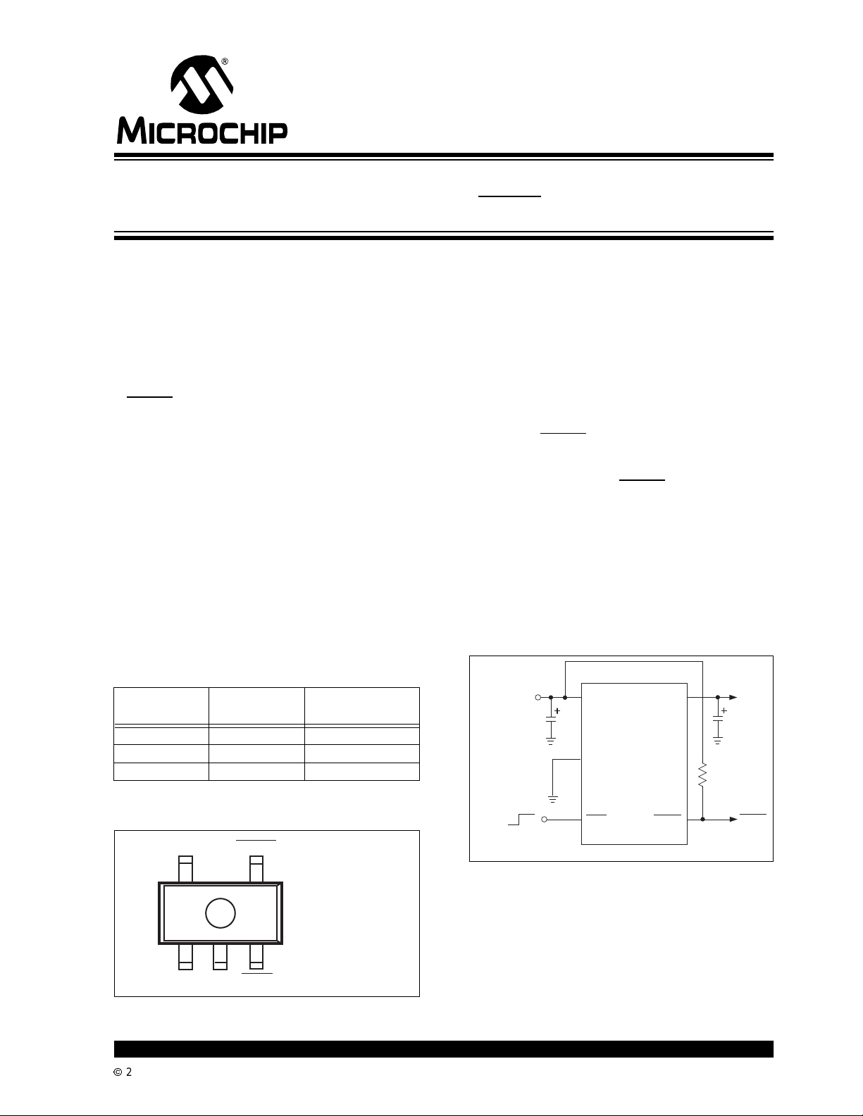
Typical Application
Device Selection Table
Junction Temp.
Part Number Package
TC2054-xxVCT 5-Pin SOT-23A* -40°C to +125°C
TC2055-xxVCT 5-Pin SOT-23A* -40°C to +125°C
TC2186-xxVCT 5-Pin SOT-23A* -40°C to +125°C
Note: *5-Pin SOT-23A is equivalent to EIAJ (SC-74A).
Range
Package Type
V
OUT
ERROR
45
V
IN
Shutdown Control
(from Power Control Lo
1
V
IN
1µF
2
GND
TC2054
TC2055
TC2186
34
SHDN
ic)
TC2054
TC2055
TC2186
2
1
V
GND
IN
2002 Microchip TechnologyInc. DS21663B-page 1
3
SHDN
5-Pin SOT-23A*
TOP VIEW
V
OUT
ERROR
5
1µF
1M
V
OUT
ERROR
TC2054/2055/2186
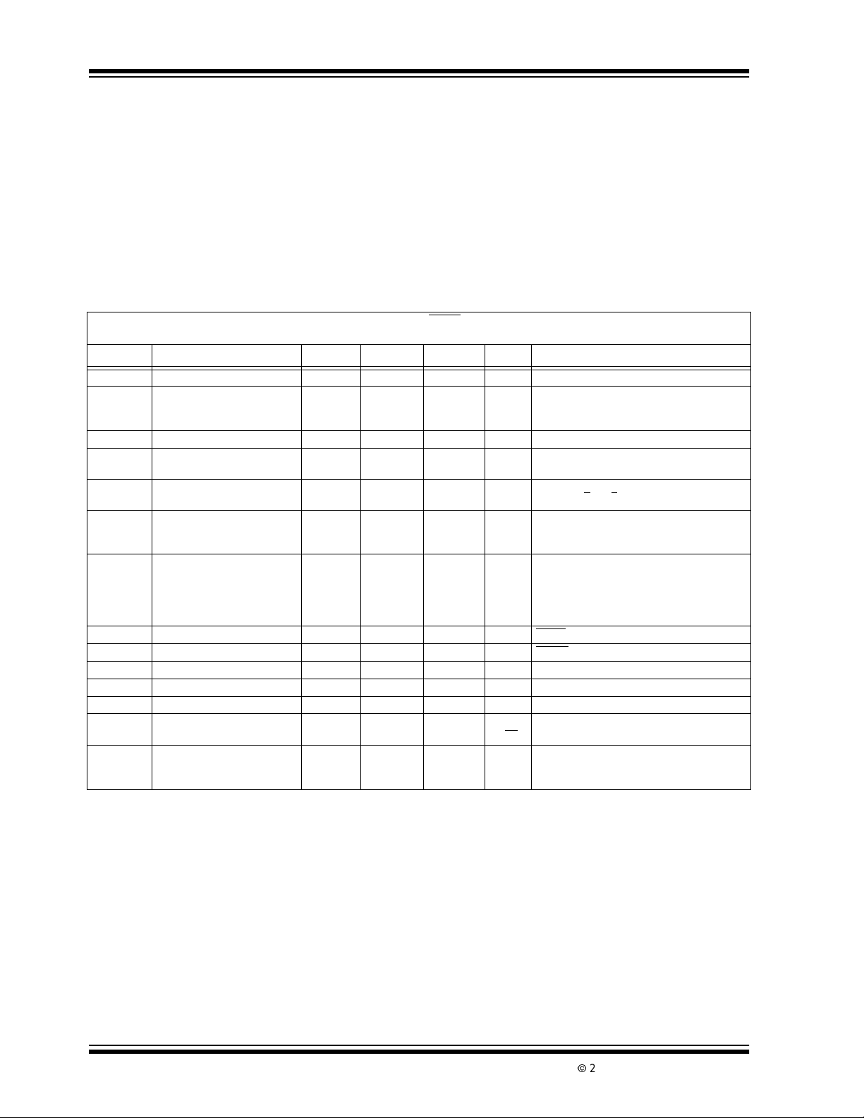
1.0 ELECTRICAL
CHARACTERISTICS
ABSOLUTE MAXIMUM RATINGS*
Input Voltage .........................................................6.5V
Output Voltage................................(-0.3) to (V
Operating Temperature ..................-40°C < T
+0.3)
IN
<125°C
J
*Stresses above those listed under “Absolute Maximum Ratings” may cause permanent damage to the
device. These are stress r atings only and functional
operation of the device attheseor any other conditions
above those indicated in the operation sections of the
specifications is not implied. Exposure to Absolute
Maximum Rating conditions for extended periods my
affect device reliability.
Storage Temperature..........................-65°C to +150°C
Maximum Voltage on Any Pin ........V
+0.3V to -0.3V
IN
TC2054/2055/2186 ELECTRICAL SPECIFICATIONS
Electrical Characteristics: VIN=VR+1V,IL=100µA, CL=3.3µF, SHDN >VIH,TA= 25°C, unless otherwise noted. BOLDFACE
type specifications apply for junction temperatureof -40°Cto +125°C.
Symbol Parameter Min Typ Max Units Test Conditions
V
IN
I
OUT
MAX
V
OUT
TCV
OUT
∆V
OUT
∆V
IN
∆V
OUT
V
OUT
V
IN–VOUT
I
IN
I
INSD
PSRR Power Supply Rejection Ratio — 50 — dB F
I
OUT
SC
∆V
OUT∆PD
eN Output Noise — 600 — nV /
t
R
Note 1: The minimum V
InputOperatingVoltage 2.7 — 6.0 V Note 1
Maximum Output Current 50
100
150
—
—
—
—
—
—
mA TC2054
TC2055
TC2186
Output Voltage VR-2.0% VR±0.4% VR+2.0% V Note 2
V
Temperature
OUT
Coefficient
/
LineRegulation — 0.05 0.5 %(VR+1V)<VIN< 6V
/
Load Regulation -1.5
—
—
-2.5
20
40
0.5
0.5
—
—
0.5
0.5
ppm/°C Note3
% TC2054;TC2055 IL=0.1mAtoIOUT
TC2186 IL=0.1mAtoIOUT
Note 4
Dropout Voltage, Note 5 —
—
—
—
2
45
90
140
—
70
140
210
mV IL=100µA
TC2015; TC2185 I
TC2185 I
Note 5
Supply Current — 55 80 µASHDN=VIH,IL=0
Shutdown Supply Current — 0.05 0.5 µASHDN=0V
≤ 120kHz
RE
Output Short Circuit Current 160 300 — mA V
OUT
Thermal Regulation — 0.04 — V/W Note 6
IL=I
√Hz
Response Time
(fromShutdown Mode)
has to meet two conditions: VIN= 2.7V and VIN=VR+V
is the regulator output voltage setting. Forexample: VR= 1.8V, 2.7V, 2.8V, 2.85V, 3.0V, 3.3V.
2: V
R
3: TCV
OUT
IN
=
V
OUTM AXVOUTMIN
-----------------------------------------------------------------------------------------
–()106×
V
OUT
—60—µsec VIN=4V
DROPOUT
∆T×
=1µF, C
C
IN
I
=0.1mA,Note 9
L
.
=0V
OUT
,F=10kHz
MAX
OUT
I
=10µF
=50mA
L
=100mA
L
=150mA
L
MAX
MAX
4: Regulation is measured at a constant junction temperature using low duty cycle pulse testing. Load regulation is tested over a
load range from 1.0mA to the maximum specified output current. Changes in output voltage due to heating effects are covered
by the thermal regulation specification.
5: Dropout voltage is defined as the input to output differential at which the output voltage drops 2% below its nominal value at a 1V
differential.
6: Thermal Regulation is defined as the change in output voltage at a time T after achange in power dissipation is applied, exclud-
ing load or line regulation effects. Specifications are for a current pulse equal to I
7: The maximum allowable power dissipation is a function of ambient temperature, the maximum allowable junction temperature
and the thermal resistance from junction-to-air (i.e. T
8: Hysteresis voltage is referenced by V
9: Time required for V
to reach 95% of VR(output voltage setting), after V
OUT
.
R
A,TJ
, θJA).
SHDN
DS21663B-page 2
at VIN= 6V for T = 10msec.
MAX
is switched from 0 to VIN.
2002 Microchip TechnologyInc.
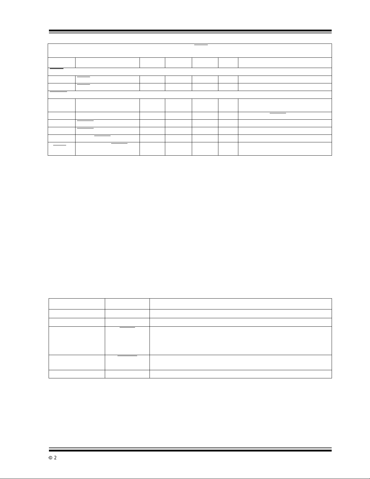
TC2054/2055/2186
Electrical Characteristics: VIN=VR+1V,IL=100µA, CL=3.3µF,SHDN >VIH,TA= 25°C, unless otherwise noted. BOLDFACE
type specificationsapply for junction temperature of -40°C to +125°C.
Symbol Parameter Min Typ Max Units Test Conditions
SHDN Input
V
IH
V
IL
ERROR OUTPUT
V
INMIN
V
OL
V
TH
V
HYS
t
DELAY
R
ERROR
Note 1: The minimum V
SHDN InputHigh Threshold 60 ——%V
SHDN Input Low Threshold — — 15 %VINVIN= 2.5V to 6.0V
Minimum VINOperating Voltage
Output Logic Low Voltage — — 400 mV 1 mA Flows to ERROR
ERROR Threshold Voltage — 0.95 x V
ERROR Positive Hysteresis — 50 — mV Note 8
V
to ERROR Delay — 2 — msec V
OUT
Resistance from ERROR to
GND
has to meet two conditions: VIN=2.7VandVIN=VR+V
2: V
is the regulator output voltage setting. For example: VR= 1.8V, 2.7V,2.8V , 2.85V, 3.0V, 3.3V.
R
3: TCV
OUT
4: Regulation is measured ata constant junction temperature using low duty cycle pulse testing. Load regulation is tested over a
load range from 1.0mA to the maximum specified output current. Changes in output voltage due to heating effects are covered
by the thermal regulationspecification.
5: Dropout voltage is defined as the input to output differential atwhich the output voltage drops 2% below its nominal value at a 1V
differential.
6: Thermal Regulation isdefined as the change in output voltage at a time T after a change in power dissipation is applied, exclud-
ing load or line regulation effects. Specifications are for a current pulse equal to I
7: The maximum allowable power dissipation isa function of ambient temperature, the maximum allowable junction temperature
and the thermal resistance from junction-to-air (i.e. T
8: Hysteresis voltage is referenced by V
9: Time required for V
IN
=
V
OUTM AXVOUTMIN
-----------------------------------------------------------------------------------------
–()106×
V
OUT
to reach 95% of VR(output voltage setting), after V
OUT
1.0 — — V V
— V SeeFigure4-2
R
— 126 — Ω VDD=2.5V,V
DROPOUT
∆T×
, θJA).
.
R
A,TJ
SHDN
= 2.5V to 6.0V
INVIN
≥ 2.7V
OUT
from VR=3Vto2.8V
OUT
OUT
.
at VIN= 6V for T =10msec.
MAX
is switched from 0 to VIN.
=2.5V
2.0 PIN DESCRIPTIONS
ThedescriptionsofthepinsarelistedinTable2-1.
TABLE 2-1: PIN FUNCTION TABLE
Pin Number Symbol Description
1V
IN
2 GND Ground terminal.
3 SHDN
4 ERROR
5V
OUT
Unregulated supply input.
Shutdown control input. The regulator is fully enabled when a logic high is
applied to this input. The regulator enters shutdown when a logic l ow is
appliedto this input. During shutdown, output voltage falls to zero, ERROR
is open circuited and supplycurrent is reducedto 0.5µA (max).
Out-of-Regulation Flag. (Open drain output). This outputgoes low when
V
is out-of-tolerance byapproximately -5%.
OUT
Regulated voltage output.
2002 Microchip TechnologyInc. DS21663B-page 3
TC2054/2055/2186
3.0 DETAILED DESCRIPTION
The TC2054, TC2055 and TC2186 are precision fixed
output voltage regulators. (If an adjustable version is
desired, please see the TC1070, TC1071 or TC1187
data sheets.) Unlike bipolar regulators, the TC2054,
TC2055 and TC2186 supply current does not increase
with load current. In addition, V
within regulation over the entire 0mA to maximum output current operating load range.
Figure 3-1 showsa typical application circuit. The regulator i s enabled any time the shutdown input (SHDN
is at or above V
SHDN
is at orbelowVIL. SHDN maybecontrolledbya
, and shutdown (disabled) when
IH
CMOS logic gate, or I/O port of a microcontroller. I f the
SHDN
input is not required, it should be connected
directly to the input supply. While in shutdown, supply
current decreases to 0.05µA(typical),V
zero volts, and ERROR
is open-circuited.
FIGURE 3-1: TYPICAL APPLICATION CIRCUIT
V
IN
1µF
BATTERY
Shutdown Control
(to CMOS Logic or Tie
if unused)
to V
IN
TC2054
GND
TC2055
TC2186
C2 Required Only
if ERROR is used as a
Processor RESET Signal
(See Text)
remains stable and
OUT
V
OUT
+
ERRORSHDN
V
1µF
C1
R1
1M
0.2µF
C2
OUT
falls to
V
OUT
BATTLOW
or RESET
FIGURE 3-2: ERROR OUTPUT OPERATION
V
OUT
V
TH
ERROR
V
IH
V
OL
)
3.2 Output Capacitor
A1µF(min)capacitorfromV
OUT
HYSTERESIS (V
to ground is required.
HYS
)
The output capacitor should have an effective series
resistance of 0.01Ω.to5Ω forV
to 5Ω forV
nected from V
<2.5V. A1µF capacitorshould be con-
OUT
to GND if t here is more than 10inches
IN
= 2.5V,and 0.05Ω.
OUT
of wire between the regulator and the AC filter capacitor,or if a batteryisusedasthepowersource.Ceramic,
tantalum and aluminum electrolytic capacitors can be
used. (Since many aluminum electrolytic capacitors
freeze at approximately -30°C, solid tantalums are recommended f or applications operating b elow -25°C).
Whenoperatingfromsourcesother than batteries,supply-noise rejection and transient response can be
improved by increasing the value of the i nput and output capacitors and employing passive f iltering techniques.
3.1 ERROR Open Drain Output
ERROR is driven low whenever V
lationbymorethan-5%(typical).This condition may be
caused by low input voltage, output current limiting or
thermal limiting. The ERROR
rated V
age value (e.g. ERROR
regardless of the programmed output volt-
OUT
=VOLat 4.75V (typ.) for a 5.0V
regulator and 2.85V (typ.) for a 3.0V regulator).
ERROR
Note that ERROR
inactive when V
output operation is shownin Figure 4-2.
isactivewhenV
rises above VTHby V
OUT
As shown in Figure 3-1, ERROR
tery low flag or as a processor RESET
addition of timing capacitor C2). R1 x C2 should be
chosen to maintain ERROR
RESET
input for at least 200msec toallow time for the
below VIHof the processor
system to stabilize. Pull-up resistor R1 can be tied to
V
OUT,VIN
The ERROR
or any other voltage less than (VIN+0.3V).
pin sink current is self-limiting to approxi-
mately 18mA.
falls out of regu-
OUT
threshold is 5% below
fallsto VTH,and
OUT
HYS
.
can be usedas a bat-
signal (with the
DS21663B-page 4
2002 Microchip TechnologyInc.

TC2054/2055/2186
4.0 THERMAL CONSIDERATIONS
4.1 Power Dissipation
The amount ofpower the regulator dissipatesis primarily a function of input and output voltage, and output
current.
The following equation is used to calculate worst case
power dissipation:
EQUATION 4-1:
≈ (VIN–V
P
D
Where:
P
D
V
IN
V
OUT
I
LOAD
MAX
= Worstcase actualpowerdissipation
= Maximum voltage on V
= Minimum regulator output voltage
MIN
= Maximum output ( load) current
MAX
The m aximum allowable power dissipation (Equation
4-2) is a functionofthe maximum ambient temperature
(T
), the maximum allowable die temperature (125
A
MAX
°C) and the thermal resistance from junction-to-air
(θ
). The 5-Pin SOT-23A package has a θJAof
JA
approximately 220°C/Watt when mounted on a typical
two layer FR4 dielectric copper clad PC board.
EQUATION 4-2:
OUT
MIN
)I
LOAD
MAX
IN
Equation 4-1 can be used in conjunction with Equation
4-2 to ensure regulator thermaloperation is within limits.For example:
Given:
V
IN
V
OUT
I
LOAD
T
A
MAX
MAX
=3.0V±5%
= 2.7V– 2.5%
MIN
= 40mA
MAX
= 55°C
Find:1. Actual power dissapation
2. Maximum allowable dissapation
Actual power dissipation:
P
D
≈ (V
IN
MAX
–V
OUT
MIN
)I
LOAD
MAX
= [(3.0 x 1.05) – (2.7 x .975)]40x 10
= 20.7mW
Maximum allowable powerdissipation:
T
T
–()
J
A
MAX
P
D
------------------------------------- -=
MAX
125 55–()
--------------------------220
MAX
θ
JA
–3
T
MAX
---------------------------------- -=
P
D
J
MAX
T
–
A
MAX
θ
JA
Where all termsare previously defined
= 318mW
In this example, the TC2054 dissipates a maximum of
only 20.7mW; far below the allowable limit of 318mW.
In a similar manner,Equation4-1 and Equation 4-2 can
be used to calculate maximum current and/or input
voltage limits.
4.2 Layout Considerations
The primary path of heat conduction out of the package
is via the package leads. Therefore, layouts having a
ground plane, wi de tracesat the pads, and widepower
supply bus lines combine to lower θ
increase the maximum allowable power dissipation
limit.
and, therefore,
JA
2002 Microchip TechnologyInc. DS21663B-page 5

TC2054/2055/2186
5.0 TYPICAL CHARACTERISTICS
Note: The graphs and tables provided following this note are a statistical summary basedon alimited number of
samples and are provided f or informational purposes only. The performance characteristics listed herein
are not tested or guaranteed. In some graphs or tables, the data presented may be outside the specified
operating range ( e.g., outside specified power supplyrange) and therefore outside the warranted range.
FIGURE 5-1: POWER SUPPLY REJECTION
RATIO
0
V
INDC
= 4V
V
INAC
= 100mV
p-p
OUTDC
= 3V
V
-20
OUT
= 100µA
I
C
OUT
= 1mF Ceramic
FIGURE 5-4: POWER SUPPLY REJECTION
RATIO
0
V
INDC
= 4V
V
INAC
= 100mV
p-p
OUTDC
= 3V
V
-20
OUT
= 150mA
I
C
OUT
= 10µF Ceramic
-40
PSRR (dB)
-60
-80
-100
10 100 1k 10k 100k 1M
f (Hz)
FIGURE 5-2: POWER SUPPLY REJECTION
RATIO
0
V
INDC
= 4V
V
INAC
= 100mV
p-p
OUTDC
= 3V
V
-20
-40
PSRR (dB)
-60
-80
-100
10 100 1k 10k 100k 1M
I
OUT
= 150mA
C
OUT
= 1µF Ceramic
f (Hz)
FIGURE 5-3: OUTPUT NOISE
10
1
C
OUT
0.1
Noise (mV/√Hz)
0.01
0.001
0.01 0.1 1 10 100 1000
Frequency (KHz)
= 1µF
-40
PSRR (dB)
-60
-80
-100
10 100 1k 10k 100k 1M
f (Hz)
FIGURE 5-5: POWER SUPPLY REJECTION
RATIO
0
V
INDC
= 4V
V
INAC
= 100mV
OUTDC
= 3V
p-p
V
-20
-40
PSRR (dB)
-60
-80
-100
10 100 1k 10k 100k 1M
f (Hz)
FIGURE 5-6: DROPOUT VOLTAGE VS. I
0.160
V
OUT
0.140
0.120
0.100
0.080
DOV (V)
0.060
0.040
0.020
0.000
= 1.8V
T = 130˚C
0
50
ILOAD (mA)
OUT
= 150mA
I
C
OUT
= 10µF Tantalum
LOAD
T = 25˚C
T = -45˚C
100 150
DS21663B-page 6
2002 Microchip TechnologyInc.

TYPICAL CHARACTERISTICS (CONT)
)
)
0
TC2054/2055/2186
FIGURE 5-7: IDDVS. TEMPERATURE
65.00
V
OUT
63.00
61.00
(mA)
59.00
DD
I
57.00
55.00
53.00
= 1.8V
VIN = 2.8V
-45 5 55 105 155
Temp (˚C
FIGURE 5-8: OUTPUT VOLTAGE VS.
TEMPERATURE
2.9
OUT
= 2.8V
V
I
OUT
= 0.1mA
2.85
2.8
2.75
(V)
2.7
OUT
V
2.65
2.6
2.55
2.5
-50 -35 -20 -5 10 25 40 55 70 85 100 115 130 145
VIN = 6.5V
VIN = 3.8V
Temperature (˚C)
VIN = 6.0V
FIGURE 5-9: OUTPUT VOLTAGE VS.
TEMPERATURE
1.9
OUT
= 1.8V
V
I
OUT
= 0.1mA
1.88
1.86
1.84
VIN = 6.0V
1.82
(V)
1.8
OUT
V
1.78
1.76
1.74
1.72
1.7
-50 -35 -20 -5 10 25 40 55 70 85 100 115 130 145
VIN = 6.5V
VIN = 2.8V
Temperature (˚C
FIGURE 5-10: OUTPUT VOLTAGE VS. OUTPUT
CURRENT
1.9
1.88
1.86
1.84
1.82
(V)
1.8
OUT
V
1.78
1.76
1.74
1.72
1.7
0 15 30 45 60 75 90 105 120 135 15
VIN = 2.8V
I
LOAD
(mA)
FIGURE 5-11: OUTPUT VOLTAGE VS. SUPPLY
VOLTAGE
2.9
OUT
= 2.8V
V
I
OUT
= 0.1mA
2.85
2.8
2.75
(V)
2.7
OUT
V
2.65
2.6
2.55
2.5
3.5 4 4.5 5 5.5 6 6.5 7
Temp = +130˚C
Temp = -45˚C
V
IN
(V)
Temp = +25˚C
FIGURE 5-12: OUTPUT VOLTAGE VS. SUPPLY
VOLTAGE
1.9
OUT
= 1.8V
V
1.88
I
OUT
= 0.1mA
1.86
1.84
1.82
(V)
1.8
OUT
V
1.78
1.76
1.74
1.72
1.7
2.7 3.2 3.7 4.2 4.7 5.2 5.7 6.2 6.7
Temp = +130˚C
Temp = +25˚C
Temp = -45˚C
V
IN
(V)
2002 Microchip TechnologyInc. DS21663B-page 7

TC2054/2055/2186
TYPICAL CHARACTERISTICS (CONT)
FIGURE 5-13: LOAD TRANSIENT RESPONSE
V = 3.8V
IN
V = 2.8V
OUT
C = 1 µF Ceramic
IN
C = 1 µF Ceramic
OUT
Frequency = 1 KHz
100mV/DIV
Load Current
V
OUT
150mA
Load
100µA
FIGURE 5-14: LOAD TRANSIENT RESPONSE IN
DROPOUT MODE
Load Transient Response in Dropout Mode
V
100mV/DIV
OUT
150mA
FIGURE 5-16: LOAD TRANSIENT RESPONSE
V = 3.0V
IN
V = 2.8V
OUT
C = 1µF Ceramic
IN
C = 10µF Ceramic
OUT
Frequency = 10KHz
100mV / DIV
Load Current
FIGURE 5-17: SHUTDOWN DELAY
V = 4.0V
IN
V = 3.0V
OUT
C = 10µF
OUT
C = 0.01µF
BYP
I = 100µA
OUT
V
OUT
150mA
Load
100µA
V
SHDN
VIN = 3.105V
VOUT = 3.006V
IN = 1µF Ceramic
C
OUT = 1µF Ceramic
C
LOAD = 20Ω
R
FIGURE 5-15: LINE TRANSIENT RESPONSE
V = 2.8V
OUT
C = 1µF Ceramic
OUT
C = 470pF
BYP
I = 100µA
50mV / DIV
2V / DIV
Input Voltage
OUT
100µA
V
6V
4V
OUT
FIGURE 5-18: SHUTDOWN WAKE-UP TIME
V = 4.0V
IN
V = 3.0V
OUT
C = 10µF
OUT
C = 0.01µF
BYP
I = 100µA
OUT
V
V
V
OUT
SHDN
OUT
DS21663B-page 8
2002 Microchip TechnologyInc.

TYPICAL CHARACTERISTICS (CONT)
TC2054/2055/2186
FIGURE 5-19: V
VIN
V
OUT
VERROR
TO ERROR DELAY
OUT
1V/Div
1V/Div
2V/Div
RPULLUP = 100kΩ
OUT = 0.3mA
I
2.8V
2.8V
0V
3.42V
3.0V
2002 Microchip TechnologyInc. DS21663B-page 9

TC2054/2055/2186
6.0 PACKAGING INFORMATION
6.1 Package Marking Information
5-Pin SOT-23A
1 & 2 = part number code+ temperaturerangeandvoltage
(V)
TC2054
Code
TC2055
Code
TC2186
Code
1.8 SA TA VA
2.5SBTBVB
2.7SCTCVC
2.8SDTDVD
2.85 SE TE VE
3.0SFTFVF
3.3SGTGVG
3 r epresents yearand 2-month period code
4 r epresents lot IDnumber
6.2 Taping Information
Component Taping Orientation for 5-Pin SOT-23A (EIAJ SC-74A) Devices
Device
Marking
User Direction of Feed
W
Standard Reel Component Orientation
TR Suffix Device
(Mark Right Side Up)
Carrier Tape, Number of Components Per Reel and Reel Size
Package Carrier Width (W) Pitch (P) Part Per Full Reel Reel Size
5-Pin SOT-23A 8 mm 4 mm 3000 7 in
DS21663B-page 10
PIN 1
P
Reverse Reel Component Orientation
RT Suffix Device
(Mark Upside Down)
2002 Microchip TechnologyInc.

6.3 Package Dimensions
SOT-23A-5
TC2054/2055/2186
.075 (1.90)
REF.
.122 (3.10)
.098 (2.50)
.020 (0.50)
.012 (0.30)
.057 (1.45)
.035 (0.90)
PIN 1
.006 (0.15)
.000 (0.00)
.122 (3.10)
.106 (2.70)
.071 (1.80)
.059 (1.50)
.037 (0.95)
REF.
10° MAX.
.010 (0.25)
.004 (0.09)
.024 (0.60)
.004 (0.10)
Dimensions: inches (mm)
2002 Microchip TechnologyInc. DS21663B-page 11

TC2054/2055/2186
NOTES:
DS21663B-page 12
2002 Microchip TechnologyInc.

TC2054/2055/2186
SALES AND SUPPORT
Data Sheets
Products supportedby a preliminary DataSheetmayhave an erratasheetdescribing minor operational differences and recommendedworkarounds.To determine if an errata sheetexists for a particulardevice, please contact one of the following:
1. Your local Microchip sales office
2. The Microchip Corporate Literature Center U.S. FAX:(480)792-7277
3. The Microchip Worldwide Site (www.microchip.com)
Pleasespecify which device, revision of silicon and Data Sheet (includeLiterature #) you are using.
New Customer Notification System
Register on our web site (www.microchip.com/cn)to receivethe most currentinformation on our products.
2002 Microchip TechnologyI nc. DS21663B-page13

TC2054/2055/2186
NOTES:
DS21663B-page 14 2002 Microchip Technology Inc.

Information contained in this publication regarding device
applications and the like is intended through suggestion only
and may be superseded by updates. Itis your responsibility to
ensure that your application meets with your specifications.
No representation or warranty is given and no liability is
assumed by Microchip Technology Incorporated with respect
to the accuracy or use ofsuch information, or infringement of
patents or other intellectual property rights arising from such
use or otherwise. Use of Microchip’s products as critical components in life support systems is not authorized except with
express written approval by Microchip. No licenses are conveyed, implicitly orotherwise, under any intellectual property
rights.
Trademarks
TheMicrochipnameandlogo,theMicrochiplogo,FilterLab,
K
EELOQ,microID,MPLAB,PIC,PICmicro,PICMASTER,
PICSTART, PRO MATE, SEEVAL and The Embedde d Control
SolutionsCompany areregiste red trademarksof MicrochipTechnologyIncorp or ated in the U.S.A. and other countries .
dsPIC, ECONOMONITOR, FanSense, FlexROM, fuzzyLAB,
In-Circuit Serial Programming, ICSP, ICEPIC, microPort,
Migratable Memory, MPASM, MPLIB, MP LINK, MPSIM,
MXDEV, PICC, PICDEM, PICDEM.net, rfPIC, Select Mode
and TotalEndurancearetrademarksofMicrochipTechnology
Incorporated in theU.S.A.
Serialized Quick Turn Programming (SQTP) is a service mark
of Microchip TechnologyIncorporated in t he U.S.A.
All other trademarks mentioned herein are property of their
respective companies.
© 2002, Microchip Technology Incorporated, Printed in the
U.S.A., All Rights Reserved.
Printed on recycled paper.
Microchip received QS-9000 quality system
certification for its worldwide headquarters,
design and wafer fabrication facilities in
Chandler and Tempe, Arizona inJuly 1999
and Mountain View, California inMarch 2002.
The Company’s quality system processes and
procedures are QS-9000 compliant for its
®
PICmicro
devices, Serial EEPROMs, microperipherals,
non-volatile memory and analog products. In
addition, Microchip’s quality system for the
design and manufacture of development
systems is ISO9001 certified.
8-bit MCUs, KEELOQ®code hopping
2002 Microchip TechnologyI nc. DS21347B - page 15

WORLDWIDE SALES AND SERVICE
AMERICAS
Corporate Office
2355 West Chandler Blvd.
Chandler, AZ 85224-6199
Tel: 480-792-7200 Fax: 480-792-7277
Technical Support: 480-792-7627
Web Address: http://www.microchip.com
Rocky Mountain
2355 West Chandler Blvd.
Chandler, AZ 85224-6199
Tel: 480-792-7966 Fax: 480-792-7456
Atlanta
500 Sugar Mill Road, Suite 200B
Atlanta, GA 30350
Tel: 770-640-0034 Fax: 770-640-0307
Boston
2 Lan Drive, Suite 120
Westford, MA 01886
Tel: 978-692-3848 Fax: 978-692-3821
Chicago
333 Pierce Road, Suite 180
Itasca, IL 60143
Tel: 630-285-0071 Fax: 630-285-0075
Dallas
4570 Westgrove Drive, Suite 160
Addison, TX 75001
Tel: 972-818-7423 Fax: 972-818-2924
Detroit
Tri-Atria Office Building
32255 Northwestern Highway, Suite 190
Farmington Hills, MI 48334
Tel: 248-538-2250 Fax: 248-538-2260
Kokomo
2767 S. Albright Road
Kokomo, Indiana 46902
Tel: 765-864-8360 Fax: 765-864-8387
Los Angeles
18201 Von Karman, Suite 1090
Irvine, CA 92612
Tel: 949-263-1888 Fax: 949-263-1338
New York
150 Motor Parkway, Suite 202
Hauppauge, NY 11788
Tel: 631-273-5305 Fax: 631-273-5335
San Jose
Microchip Technology Inc.
2107 North First Street, Suite 590
San Jose, CA 95131
Tel: 408-436-7950 Fax: 408-436-7955
Toronto
6285 Northam Drive, Suite 108
Mississauga, Ontario L4V 1X5, Canada
Tel: 905-673-0699 Fax: 905-673-6509
ASIA/PACIFIC
Australia
Microchip Technology Australia Pty Ltd
Suite 22, 41Rawson Street
Epping 2121, NSW
Australia
Tel: 61-2-9868-6733 Fax: 61-2-9868-6755
China - Beijing
Microchip Technology Consulting (Shanghai)
Co., Ltd., Beijing Liaison Office
Unit 915
Bei Hai Wan Tai Bldg.
No. 6 Chaoyangmen Beidajie
Beijing, 100027, No. China
Tel: 86-10-85282100 Fax: 86-10-85282104
China - Chengdu
Microchip Technology Consulting (Shanghai)
Co., Ltd., Chengdu Liaison Office
Rm. 2401, 24th Floor,
Ming Xing Financial Tower
No. 88 TIDU Street
Chengdu 610016, China
Tel: 86-28-6766200 Fax: 86-28-6766599
China - Fuzhou
Microchip Technology Consulting (Shanghai)
Co., Ltd., Fuzhou Liaison Office
Unit 28F, World Trade Plaza
No. 71 Wusi Road
Fuzhou 350001, China
Tel: 86-591-7503506 Fax: 86-591-7503521
China - Shanghai
Microchip Technology Consulting (Shanghai)
Co., Ltd.
Room 701, Bldg. B
Far East International Plaza
No. 317 Xian Xia Road
Shanghai, 200051
Tel: 86-21-6275-5700 Fax: 86-21-6275-5060
China - Shenzhen
Microchip Technology Consulting (Shanghai)
Co., Ltd., Shenzhen Liaison Office
Rm. 1315, 13/F , Shenzhen Kerry Centre,
Renminnan Lu
Shenzhen 518001, China
Tel: 86-755-2350361 Fax: 86-755-2366086
Hong Kong
Microchip Technology Hongkong Ltd.
Unit 901-6, Tower 2, Metroplaza
223 Hing F ong Road
Kwai Fong, N.T., Hong Kong
Tel: 852-2401-1200 Fax: 852-2401-3431
India
Microchip Technology Inc.
India Liaison Office
Divyasree Chambers
1 Floor, Wing A (A3/A4)
No. 11, O’Shaugnessey Road
Bangalore, 560 025, India
Tel: 91-80-2290061 Fax: 91-80-2290062
Japan
Microchip Technology Japan K.K.
Benex S-1 6F
3-18-20, Shinyokohama
Kohoku-Ku, Yokohama-shi
Kanagawa, 222-0033, Japan
Tel: 81-45-471- 6166 Fax: 81-45-471-6122
Korea
Microchip Technology Korea
168-1, Youngbo Bldg. 3Floor
Samsung-Dong, K angnam-Ku
Seoul, Korea 135-882
Tel: 82-2-554-7200 Fax: 82-2-558-5934
Singapore
Microchip Technology Singapore Pte Ltd.
200 Middle Road
#07-02 Prime Centre
Singapore, 188980
Tel: 65-6334-8870 Fax: 65-6334-8850
Taiwan
Microchip Technology Taiwan
11F-3, No. 207
Tung HuaNorth Road
Taipei, 105, Taiwan
Tel: 886-2-2717-7175 Fax: 886-2-2545-0139
EUROPE
Denmark
Microchip Technology Nordic ApS
Regus Business Centre
Lautrup hoj 1-3
Ballerup DK-2750 Denmark
Tel: 45 4420 9895 Fax: 45 4420 9910
France
Microchip Technology SARL
Parc d’Activite du Moulin de Massy
43 Rue du Saule Trapu
Batiment A - ler Etage
91300 Massy, France
Tel: 33-1-69-53-63-20 Fax: 33-1-69-30-90-79
Germany
Microchip Technology GmbH
Gustav-Heinemann Ring 125
D-81739 Munich, Germany
Tel: 49-89-627-144 0 Fax: 49-89-627-144-44
Italy
Microchip Technology SRL
Centro Direzionale Colleoni
Palazzo Taurus 1 V. Le Colleoni 1
20041 Agrate Brianza
Milan, Italy
Tel: 39-039-65791-1 Fax: 39-039-6899883
United Kingdom
Arizona Microchip Technology Ltd.
505 Eskdale Road
Winnersh Triangle
Wokingham
Berkshire, EnglandRG41 5TU
Tel: 44 118 921 5869 Fax: 44-118 921-5820
03/01/02
*DS21663B*
DS21663B-page 16
2002 Microchip Technology Inc.
 Loading...