


TC1321
10-Bit Digital-to-Analog Converter with Two-Wire Interface
Features
• 10-Bit Digital-to-Analog Converter
• 2.7-5.5V Single Supply Operation
2
•SimpleSMBus/I
CTMSerial Interface
• Low Power: 350µA Operation, 0.5µA Shutdown
• 8-Pin SOIC and 8-Pin MSOP Packages
Applications
• Programmable VoltageSources
• Digital Controlled Amplifiers/Attenuators
• Process Monitoring and Control
Device Selection Table
Part
Number
TC1321EOA 8-Pin SOIC (Narrow) -40°C to +85°C
TC1321EUA 8-Pin MSOP -40°C to +85°C
Package Temperature Range
General Description
The TC1321 is a serially accessible 10-bit voltage output digital-to-analog converter (DAC). The DAC produces an output voltage that ranges from ground to an
externally supplied reference voltage. It operates from
a singlepower supply that can range from 2.7V to 5.5V,
making it ideal for a wide range of applications. Built
into the part is a Power-on Reset function that ensures
that the device starts at a known condition.
Communicationwith the TC1321 is accomplishedviaa
simple 2-wire SMBus/I
2
C compatible serial port, with
theTC1321 actingas a slave only device. The host can
enablethe SHDN bit in the CONFIG register to activate
the Low Power Standby mode.
Package Type
8-Pin MSOP and
8-Pin SOIC (Narrow)
V
1
REF
27
SDA
SCL
GND
TC1321
36
45
8
V
DD
DAC-OUT
NC
V
OUT
Typical Application
V
IN
V
DD
(8)
TC1321
V
V
REF
2002 Microchip TechnologyInc. DS21387B-page 1
(1)
Serial Port
(3)
SCLK
Microcontroller
DAC
(2)
SDAT
OUT
(5)
–
+
V
ADJUST
TC1321
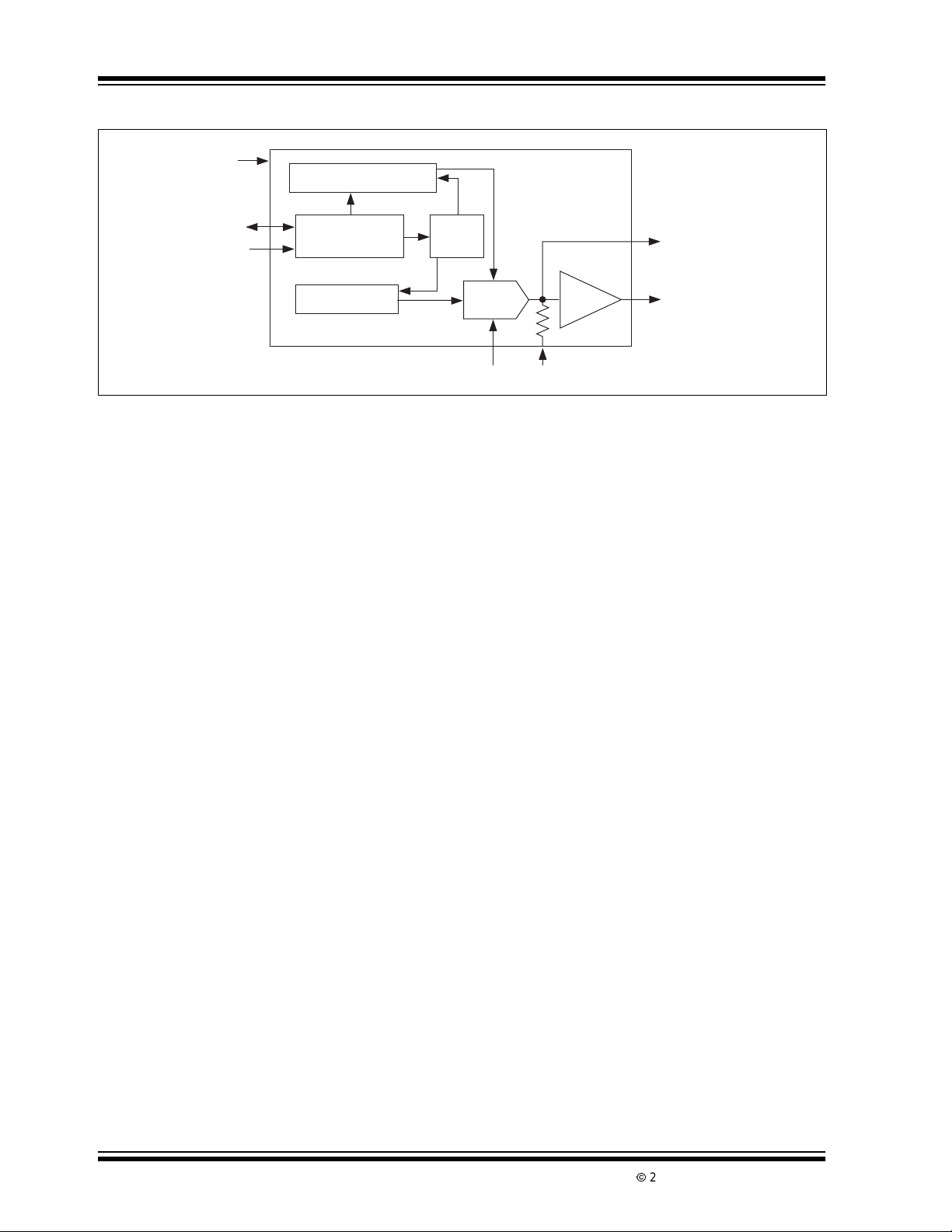
Functional Block Diagram
V
DD
Configuration Register
TC1321
SDA
SCL
Serial Port
Interface
Data Register
Control
DAC
V
REF
GND
DAC-OUT
V
OUT
DS21387B-page 2
2002 Microchip TechnologyInc.
TC1321
1.0 ELECTRICAL
CHARACTERISTICS
*Stresses above those listed under "Absolute Maximum
Ratings" may cause permanent damage to the device. These
are stress ratings only and functional operation of t he device
at these or any other conditions above those indicated in the
Absolute Maximum Ratings*
Supply Voltage (VDD).............................................+6V
VoltageonanyPin ...(GND–0.3V)to(V
DD
+0.3V)
operation sections of the specifications is not implied.
Exposure to Absolute Maximum Rating conditions for
extended periods may affectdevice reliability.
Current on any Pin............................................ ±50mA
Package Thermal Resistance(θ
Operating Temperature (T
StorageTemperature (T
A
STG
)............ 330°C C/W
JA
)........................ See Below
)..............-65°C to +150°C
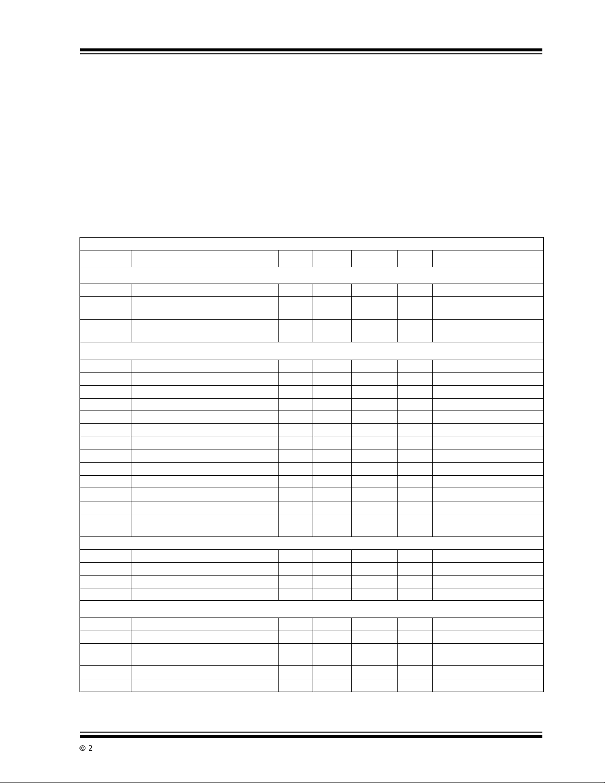
TC1321 ELECTRICAL SPECIFICATIONS
Electrical Characteristics: VDD= 2.7V to 5.5V, -40°C≤ TA≤ +85°C,V
Symbol Parameter Min Typ Max Unit Test Conditions
Power Supply
V
DD
I
DD
I
DD-STANDBY
SupplyVoltage 2.7 — 5.5 V
Operating Current — 350 500 mA VDD=5.5V,V
Standby SupplyCurrent — 0.1 1 µAVDD=3.3V
Static Performance - Analog Section
Resolution — — 10 Bits
INL Integral Non-Linearity at FS, T
= +25°C — — ±4.0 LSB (Note 2)
A
FSE Full Scale Error — — ±3 %FS
DNL Differential Non-Linearity, T
V
OS
TCV
OS
Offset Error at V
OUT
Offset Error Tempco at V
= +25°C -1 — +2 LSB All Codes (Note 2)
A
—±0.3 ±8 mV(Note 2)
OUT
—10 —µv/°C
PSRR Power Supply Rejection Ratio — 80 — dB V
V
I
REF
V
R
I
OUT
I
SC
REF
SW
OUT
Voltage Reference Range 0 — VDD–1.2 V
Reference Input Leakage Current — — ±1.0 µA
Voltage Swing 0 — V
Output Resistance @ V
OUT
—5.0 — Ω R
Output Current(Source or Sink) — 2 — mA
Output Short-Circuit Current
V
=5.5V
DD
—
—
Dynamic Performance
SR VoltageOutputSlewRate — 0.8 — V/µs
t
SETTLE
t
WU
Output Voltage Full Scale Settling Time — 10 — µsec
Wake-up Time — 20 — µs
Digital Feed Through and Crosstalk — 5 — nV-s SDA = V
Serial Port Interface
V
IH
V
IL
V
OL
C
IN
I
LEAK
Note 1: SDA and SCL must be connected to V
LogicInputHigh 2.4 — V
Logic Input Low — — 0.6 —
SDA OutputLow —
—
Input Capacitance SDA, SCL — 5 0.4 pF
I/O Leakage — — ±1.0 µA
or GND.
2: Measured at V
≥ 50mV referredto GND to avoid output buffer clipping.
OUT
DD
= 1.2 unless otherwisenoted.
REF
REF
30
20
—
—
50
50
DD
0.4
0.6
Serial Port Inactive (Note 1)
REF
Serial Port Inactive (Note 1)
at DC
DD
VV
≤ (VDD–1.2V)
REF
(Ω)
OUT
mAmASource
Sink
,SCL=100kHz
DD
V
VVIOL= 3mA (Sinking Curre nt)
I
=6mA
OL
=1.2V
2002 Microchip TechnologyInc. DS21387B-page 3
TC1321
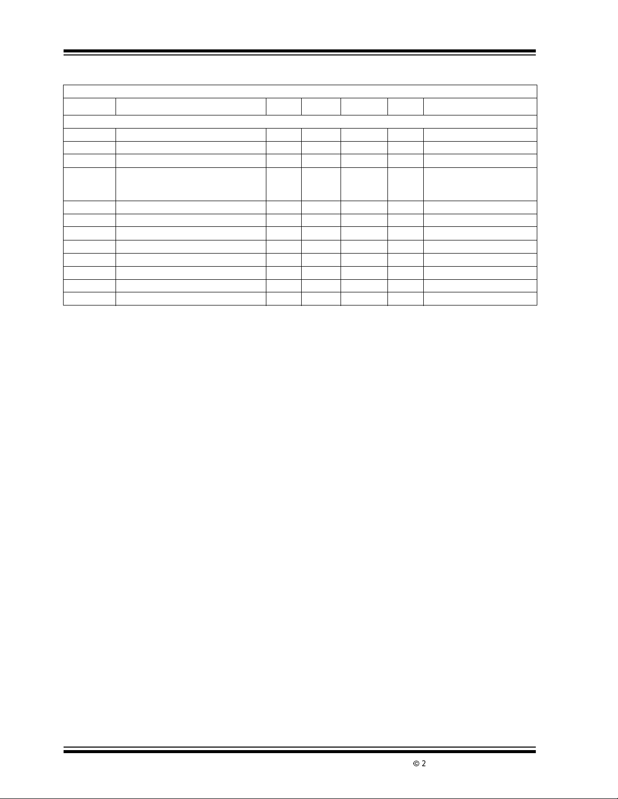
TC1321 ELECTRICAL SPECIFICATIONS (CONTINUED)
Electrical Characteristics: VDD= 2.7V to 5.5V, -40°C≤ TA≤ +85°C,V
Symbol Parameter Min Typ Max Unit Test Conditions
Serial Port AC Timing
f
SMB
t
IDLE
t
H(START)
t
SU(START)
t
SU(STOP)
t
H-DATA
t
SU-DATA
t
LOW
t
HIGH
t
F
t
R
t
POR
Note 1: SDA and SCL must be connected to V
SMBus Clock Frequency 10 — 100 kHz
BusFreeTimePriortoNewTransition 4.7 — — µsec
START Condition Hold Time 4.0 — — µsec
START Condition Setup Time 4.7 — — µsec 90%SCLto10%SDA
STOP Condition Setup Time 4.0 — — µsec
Data In Hold Time 100 — — nsec
Data In Setup Time 100 — — nsec
Low Clock Period 4.7 — — µsec 10% to 10%
High Clock Period 4 — — µsec 90% to 90%
SMBus Fall Time — — 300 nsec 90% to 10%
SMBus Rise Time — — 1000 nsec 10%to90%
Power-on Reset Delay — 500 — µsec VDD ≥ V
or GND.
2: Measured at V
≥ 50mV referredto GND to avoid output buffer clipping.
OUT
DD
= 1.2 unless otherwisenoted.
REF
(forRepeated START
Condition)
(Rising Edge)
POR
DS21387B-page 4
2002 Microchip TechnologyInc.

2.0 PIN DESCRIPTIONS
The descriptions of the pins are listed in Table 2-1.
TABLE 2-1: PIN F UNCTION TABLE
Pin Number Symbol Type Description
1V
2 SDA Bi-Directional Bi-directional. Serial data is transferred on the SMBus in both directions
3 SCL Input Input. SMBus serial clock. Clocks data into and out of the TC1321.
4 GND Power Ground.
5V
6 NC None No connection.
7 DAC-OUT Output Output. Unbuffered DAC output voltage. This voltage is a function of the
8V
REF
OUT
DD
Input Input. Voltage Reference Input can range from 0V to 1.2V below VDD.
usingthispin.
Output Output. Buffered DAC output voltage. This voltage is a function of the
reference voltageandthe contents of the DATA register.
reference voltageandthe contents of the DATA register. This outputis
unbuffered and care must be taken that the pin is connectedonlyto a
high-impedancenode.
Power Positive power supply input.See electrical specifications.
TC1321
2002 Microchip TechnologyInc. DS21387B-page 5
TC1321
3.0 DETAILED DESCRIPTION
The TC1321 is a monolithic 10-bit digital-to-analog
converterthatis designedto operate from a singlesupply that can range from2.7V to 5.5V.TheDAC consists
of a data register (DATA), a configuration register
(CONF), and a current output amplifier. The TC1321
uses an external reference which also determines the
maximum output voltage.
The TC1321 uses a current steering DAC based on an
array of mat ched current sources. This current, along
with a pr ecision resistor, converts the contents of the
Data Register and V
given by:
V
OUT=VREF
3.1 Reference Input
The r eference pin, V
inputand because of this,theload regulationof the referencesourceneedsonlytobeabletotolerate leakage
levels of current (less than 1µA). V
age r ange from 0 to (V
typically 10pF.
3.2 Output Amplifier
into an output voltage, V
REF
(DATA/1024)
, is a buffered high-impedance
REF
accepts a volt-
– 1. 2V). Input capacitance is
DD
REF
OUT
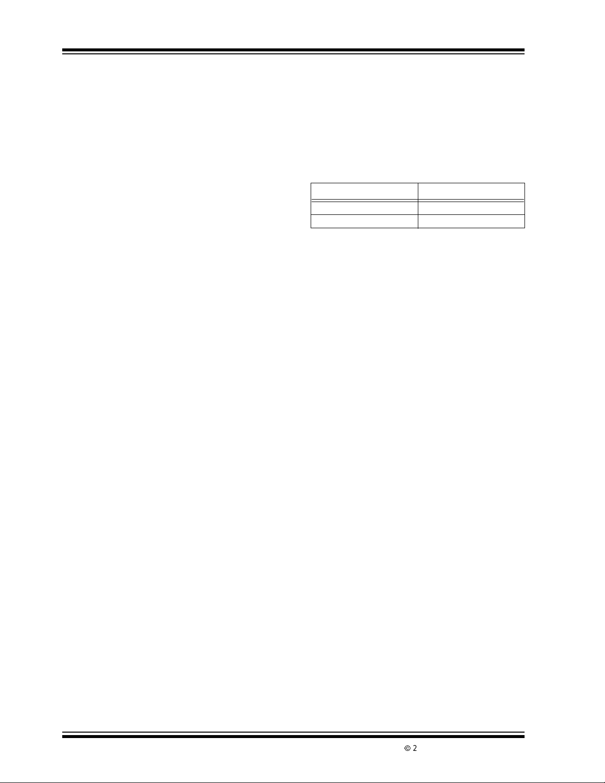
3.3 Standby Mode
The TC1321 allows the host to put it into a Low Power
(I
=0.5µA, typical) Standby mode. In this mode, the
DD
D/A conversion is halted. The SMBus port operates
normally. Standby mode is enabled by setting the
SHDN bit in the CONFIG register. The table below
summarizes this operation.
TABLE 3-1: STANDBY MODE OPERATION
SHDN Bit Operating Mode
0Normal
1 Standby
3.4 SMBus Slave Address
The TC1321 is internally programmedto have a default
SMBus address value of 1001 000b. Seven other
addresses are available by custom order (contact factory). See Figure 3-1 for location of address bits in
SMBus protocol.
The TC1321 DAC output i s buffered with an internal
unitygain rail-to-railinput/outputamplifierwitha typical
slew rate of 0.8V/µsec. Maximum full scale transition
settling time is 10µsec to within ±1/2LSB when loaded
with 1kΩ in parallel with 100pF.
DS21387B-page 6
2002 Microchip TechnologyInc.

FIGURE 3-1: SMBus PROTOCO LS
y
Write 1-Byte Format
S Address
7-Bits
Slave Address Command Byte: selects
R/W
0
ACK
Write 2-Byte Format
S
Address R/W
Slave Address
ACK
0
Read 1-Byte Format
Address
S
7-Bits
Slave Address
R/W
0
ACK
8-Bits
Command Byte: selects
which register you are
reading from.
ACKCommand
Read 2-Byte Format
Address
S
7-Bits
Slave Address
R/W
0
ACK
8-Bits
Command Byte: selects
which register you are
reading from.
ACKCommand
ACKCommand
8-Bits
which register you are
writing to.
ACKCommand
8-Bits7-Bits
Command Byte: selects
which register you are
writing to.
Address R/W ACK
S
7-Bits
Slave Address: repeated
due to change in data
flow direction.
Address R/W ACK
S
7-Bits
Slave Address: repeated
due to change in data
flow direction.
Data
8-Bits
Data Byte: data goes
into the register set
by the command byte.
Data
8-Bits 8-Bits
Data Byte: data goes
into the register set
by the command byte.
Data
1
1
8-Bits
Data Byte: reads from
the register set by the
command byte.
Data
8-Bits 8-Bits
Data Byte: reads from
the register set by the
command byte.
TC1321
ACK P
ACK Data
NACK P
ACK NACK P
Data
ACK
P
Receive 1-Byte Format
Address R/W ACK
S
7-Bits
S = START Condition
P = STOP Condition
Shaded = Slave Transmission
1
Receive 1-Byte Format
Address
S
7-Bits
S = START Condition
P = STOP Condition
Shaded = Slave Transmission
R/W
1
ACK
Data NACK
8-Bits
Data Byte: reads data from
the register commanded by
the last read byte or write
byte transmission.
Data DataACK P
8-Bits 8-Bits
Data Byte: reads data from
the register commanded by
the last read byte or write
b
te transmission.
P
NACK
2002 Microchip TechnologyInc. DS21387B-page 7

TC1321
4.0 SERIAL PORT OPERATION
The Serial Clock input (SCL) and bi-directional data
port (SDA) form a 2-wire bi-directional serial port for
programming and interrogating the TC1321. The
followingconventionsare used i n this bus ar chitecture.
TABLE 4-1: TC1321 SERIAL BUS
CONVENTIONS
Term Explanation
Transmitter The device sendingdatatothe bus.
Receiver The device receiving data from the bus.
Master The device which controls the bus: initiating
transfers (START), generating the clock, and
terminating transfers (STOP).
Slave The device addressed by the master.
START A unique condition signaling the beginning of
a transfer indicated by SDA falling
(High - Low) while SCL is high.
STOP A uniquecondition signaling the end of a
ACK A Receiver Acknowledges the receipt of each
Busy Communicationis not possible becausethe
Not Busy Whenthebus is IDLE, bothSDAandSCLwill
DataValid The stateof SDA must remain stableduring
All transfers take place under control of a host, usually
a CPU or microcontroller, acting as the Master, which
provides the clock signal f or all transfers. The TC1321
always operates as a Slave. The serialprotocol is illustratedinFigure 3-1. All datatransfershavetwophases;
all bytes are transferred MSB first. Accesses are initiated by a START condition (START), followed by a
device address byte and one or more data bytes. The
device address byte includes a Read/Write
bit. Each access must be terminated by a STOP Condition (STOP). A convention called Acknowledge
(ACK)confirmsreceiptof eachbyte.NotethatSDAcan
change only during periods when SCL is LOW (SDA
changes while SCL is HIGH are reserved for START
and STOP conditions).
transfer indicatedby SDA rising (Low - High)
while SCL is high.
byte withthisunique condition.TheReceiver
drives SDA low during SCL high of the ACK
clockpulse. The Master provides the clock
pulse for the ACK cycle.
busisinuse.
remain high.
theHighperiodofSCLinorderforadatabit
to be considered valid. SDA only changes
state while SCL is lowduringnormal data
transfers. ( See START and STOP
conditions.)
selection
4.1 S TART Condition (START)
The TC1321 continuously monitors the SDA and SCL
lines for a STARTcondition (a HIGH to LOW transition
of SDA while SCL is HIGH), and will not respond until
this condition is met.
4.2 Address Byte
Immediately following the START condition, the host
must transmit the address byte to the TC1321. The
7-bit SMBus address for the TC1321 is 1001000.The
7-bit address transmitted in the s erial bit stream must
match for the TC1321to respond with an Acknowledge
(indicating the TC1321 is on the bus and ready to
accept data). The eighth bit in the Address Byte is a
Read-Write
bit. This bit is a 1 for a read operation or 0
for a write operation. During the first phase of any
transfer, this bit will be set = 0 to indicate that the
command byte is being written.
4.3 Ac knowledge (ACK)
Acknowledge (ACK) provides a positive handshake
between the host and the TC1321. The host releases
SDA aftertransmittingeight bits, then generatesaninth
clockcycletoallowtheTC1321topulltheSDAline
LOW to Acknowledge that it successfully received the
previous eight bits of data or address.
4.4 Data Byte
After a successful ACK of the address byte, the host
must transmit the data byte to be written or clock out
the data to be read. (See the appropriate timing diagrams.) ACK will be generatedafter a successful wr ite
of a data byte into the TC1321.
4.5 Stop Condition (STOP)
Communications must be terminated by a STOP condition (a LOW to HIGH transition of SDA while SCL i s
HIGH). The STOP condition must becommunicatedby
the transmittertotheTC1321.Refer to Figure 4-1,Timing Diagramsfor serial bus timing.
DS21387B-page 8
2002 Microchip TechnologyInc.
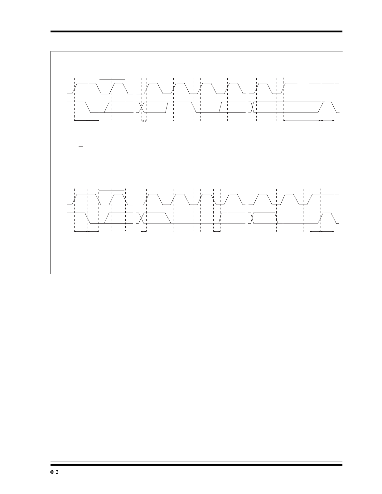
FIGURE 4-1: TIMING DIAGRAMS
SMBus Write Timing Diagram
I
LOW
B
I
HIGH
CDEFG H
A
SCL
SDA
TC1321
IJ
K
t
SU(START)tH(START)
A = START Condition
B = MSB of Address Clocked into Slave
C = LSB of Address Clocked into Slave
D = R/W Bit Clocked into Slave
SMBus Read Timing Diagram
A
I
LOW
SCL
SDA
t
SU(START)tH(START)
A = START Condition
B = MSB of Address Clocked into Slave
C = LSB of Address Clocked into Slave
D = R/W Bit Clocked into Slave
E = Slave Pulls SDA Line Low
t
SU-DATA
E = Slave Pulls SDA Line Low
F = Acknowledge Bit Clocked into Master
G = MSB of Data Clocked into Master
H = LSB of Data Clocked into Master
B
I
HIGH
CDEFG HIJ
t
SU-DATA
F = Acknowledge Bit Clocked into Master
G = MSB of Data Clocked into Slave
H = LSB of Data Clocked into Slave
I = Slave Pulls SDA Line Low
I = Acknowledge Clock Pulse
J = STOP Condition
K = New START Condition
t
H-DATA
J = Acknowledge Clocked into Master
K = Acknowledge Clock Pulse
L = STOP Condition, Data Executed by Slave
M = New START Condition
t
SU(STOP)tIDLE
KL
t
SU(STOP)tIDLE
M
2002 Microchip TechnologyInc. DS21387B-page 9

TC1321
4.6 Register Set and Programmer’s
Model
TABLE 4-2: TC1321 COMMAND SET
(SMBus READ_BYTE AND
WRITE_BYTE)
Command By te Description
Command Code Function
RWD 00h Read/Write
RWCR 01h Read/Write
(CONFIG)
TABLE 4-3: CONFIGURATION REGISTER
(CONFIG), 8-BIT, READ/WRITE
Configuration Register (CONFIG)
D[7] D[6] D[5] D[4] D[3] D[2] D[1] D[0]
Reserved SHDN
Bit POR Function Type Operation
D[0] 0 Standby Switch Read/
D[7]-D[1] 0 Reserved;
Always returns
Zero when Read
Data (DATA)
Configuration
1 = Standby
0=Normal
Write
N/A N/A
TABLE 4-4:
DATA REGISTER (DATA),
10-BIT, READ/WRITE
Data Register (DATA) for 1st Byte
D[9] D[8] D[7] D[6] D[5] D[4] D[3] D[2]
MSB X X X X X X X
Data Register (DATA) for 2nd Byte
D[1] D[0] XXXXXX
XLSBX X X X X X
The DAC output voltage is a function of r eference voltage and the binary value of the contents of the register
DATA.The transfer functionis given by the expression:
EQUATION 4-1:
DATA
V
OUT=VREF
x
1024
4.7 Register Set Summary
The TC1321’s register set is summarized in Table 4-5
below.All registers are 10-bits wide.
TABLE 4-5: TC1321 REGI STER SET
SUMMARY
Name Description POR State Read Write
Data DATARegister
(2-Byte Format)
Config CONFIG Register 0000 0000b XX
0000000000b XX
DS21387B-page 10
2002 Microchip TechnologyInc.

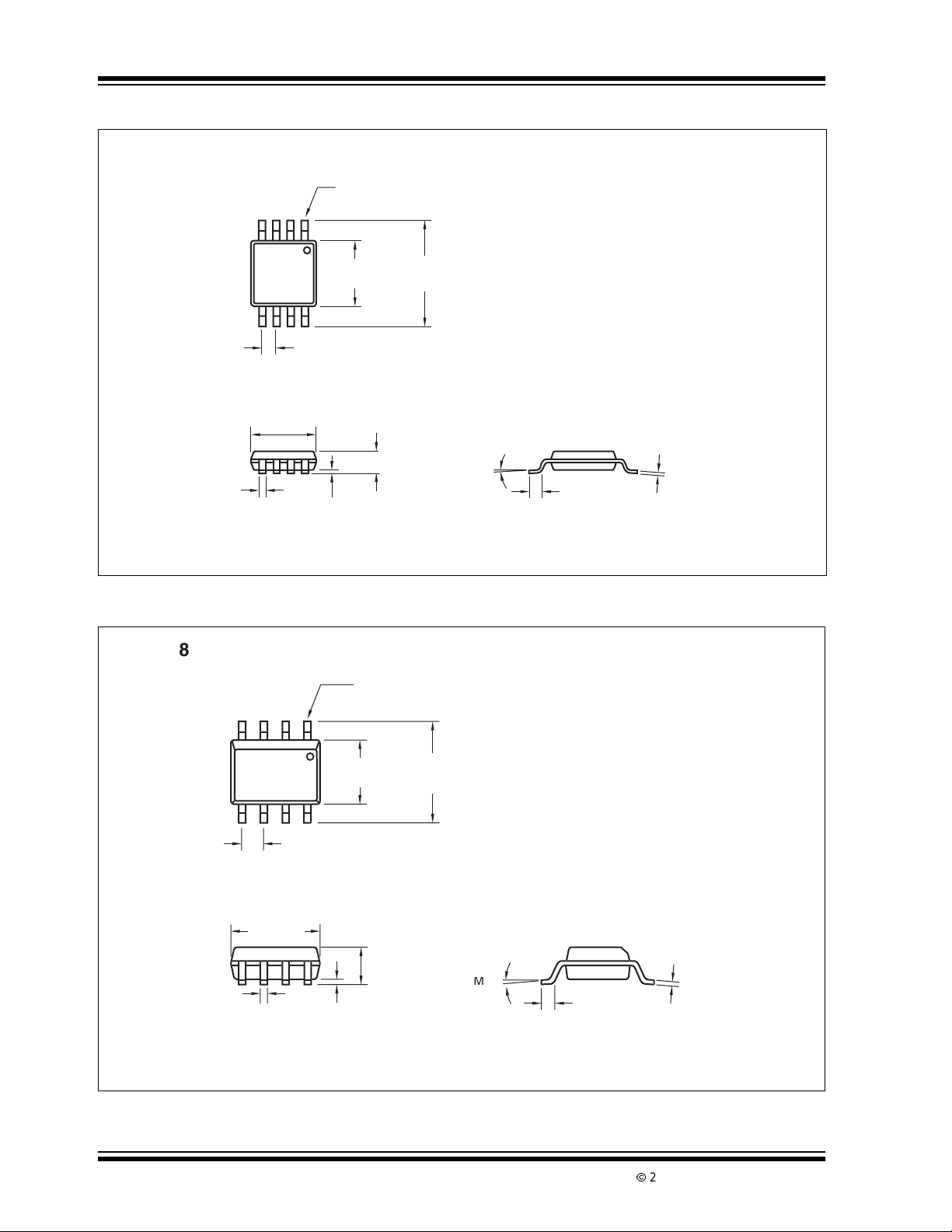
5.0 PACKAGING INFORMATION
5.1 Package Marking Information
Package marking data not available at this time.
5.2 Taping Forms
Component Taping Orientation for 8-Pin MSOP Devices
PIN 1
TC1321
User Direction of Feed
W
P
Standard Reel Component Orientation
for TR Suffix Device
Carrier Tape, Number of Components Per Reel and Reel Size
Package Carrier Width (W) Pitch (P) Part Per Full Reel Reel Size
8-Pin MSOP 12 mm 8 mm 2500 13 in
Component Taping Orientation for 8-Pin SOIC (Narrow) Devices
User Direction of Feed
PIN 1
W
P
Standard Reel Component Orientation
for TR Suffix Device
Carrier Tape, Number of Components Per Reel and Reel Size
Package Carrier Width (W) Pitch (P) Part Per Full Reel Reel Size
8-Pin SOIC (N) 12 mm 8 mm 2500 13 in
2002 Microchip TechnologyInc. DS21387B-page 11
TC1321
.
8
)
)
)
)
)
)
)
)
)
)
)
)
)
)
)
)
C
5.3 Package Dimensions
8-Pin MSOP
PIN 1
.026 (0.65) TYP.
.016 (0.40)
.010 (0.25)
-Pin SOI
.122 (3.10)
.114 (2.90)
.006 (0.15)
.002 (0.05)
.122 (3.10)
.114 (2.90)
.197 (5.00)
.189 (4.80)
.043 (1.10)
MAX.
6° MAX.
.008 (0.20)
.005 (0.13)
.028 (0.70)
.016 (0.40)
Dimensions: inches (mm)
DS21387B-page 12
.050 (1.27) TYP
.197 (5.00
.189 (4.80
.020 (0.51
.013 (0.33
.157 (3.99
.150 (3.81
.010 (0.25
.004 (0.10
.244 (6.20
.228 (5.79
.069 (1.75
.053 (1.35
.050 (1.27
.016 (0.40
.010 (0.25
.007 (0.18
Dimensions: inches (mm)
2002 Microchip TechnologyInc.

NOTES:
TC1321
2002 Microchip TechnologyInc. DS21387B-page 13

TC1321
SALES AND SUPPORT
Data Sheets
Products supportedby a preliminary Data Sheet may have an errata sheet describing minor operational differences and recommendedworkarounds.To determine if an errata sheet exists for a particulardevice, please contactoneof the following:
1. Yo ur local Microchip sales office
2. The MicrochipCorporate Literature Center U.S. FAX:(480) 792-7277
3. The Microchip Worldwide Site (www.microchip.com)
Pleasespecify which device, revision of silicon and Data Sheet (includeLiterature#) you are using.
New Customer Notification System
Register on our web site (www.microchip.com/cn) to receive the most current information on our products.
DS21387B-page 14
2002 Microchip TechnologyInc.

TC1321
Information contained in this publication regarding device
applications and the like is intended through suggestion only
and may be superseded by updates. It is your responsibility to
ensure that your application meets with your specifications.
No representation or warranty is given and no liability is
assumed by Microchip Technology Incorporated with respect
to the accuracy or use of such information, or infringement of
patents or other intellectual property rights arising from such
use or otherwise. Use of Microchip’s products as critical components in life support systems is not authorized except with
express written approval by Microchip. No licenses are conveyed, implicitly or otherwise, under any intellectual property
rights.
Trademarks
The Microchip name and logo, the Microchip logo, FilterLab,
K
EELOQ,microID,MPLAB,PIC,PICmicro,PICMASTER,
PICSTART, PRO MATE, SEEVAL and The Embedded Control
SolutionsCompany areregiste red trademarksof MicrochipTechnologyIncorp or ated in the U.S.A. and other countries .
dsPIC, ECONOMONITOR, FanSense, FlexR OM , fuzzyLAB,
In-Circuit Serial Programming, ICSP, ICEPIC, microPort,
Migratable Memory, MPA SM, MPLIB, MPLINK, MPSIM,
MXDEV, PICC, PICDEM, PICDEM .n et , rfPIC, Select Mode
and TotalEndurancearetrademarksofMicrochipTechnology
Incorporated in the U.S.A.
Serialized Quick Turn Programming (SQTP) is a service mark
of Microchip TechnologyIncorporated in t he U.S.A.
All other trademarks mentioned herein are property of their
respective companies.
© 2002, Microchip Technology Incorporated, Printed in the
U.S.A., All Rights Reserved.
Printed on recycled paper.
Microchip received QS-9000 quality system
certification for its worldwide headquarters,
design and wafer fabrication facilities in
Chandler and Tempe, Arizona in July 1999
and Mountain View,California in March 2002.
The Company’s quality system processes and
procedures are QS-9000 compliant for its
®
PICmicro
devices, Serial EEPROMs, microperipherals,
non-volatile memory and analog products. In
addition, Microchip’s quality system for the
design and manufacture of development
systemsisISO 9001certified.
2002 Microchip TechnologyInc. DS21387B-page 15
8-bit MCUs, KEELOQ®code hopping
WORLDWIDE SALES AND SERVICE
AMERICAS
Corporate Office
2355 West Chandler Blvd.
Chandler, AZ 85224-6199
Tel: 480-792-7200 Fax: 480-792-7277
Technical Support: 480-792-7627
Web Address: http://www.microchip.com
Rocky Mountain
2355 West Chandler Blvd.
Chandler, AZ 85224-6199
Tel: 480-792-7966 Fax: 480-792-7456
Atlanta
500 Sugar Mill Road, Suite 200B
Atlanta, GA 30350
Tel: 770-640-0034 Fax: 770-640-0307
Boston
2 Lan Drive, Suite 120
Westford, MA 01886
Tel: 978-692-3848 Fax: 978-692-3821
Chicago
333 Pierce Road, Suite 180
Itasca, IL 60143
Tel: 630-285-0071 Fax: 630-285-0075
Dallas
4570 Westgrove Drive, Suite 160
Addison, TX 75001
Tel: 972-818-7423 Fax: 972-818-2924
Detroit
Tri-Atria Office Building
32255 Northwestern Highway, Suite 190
Farmington Hills, MI 48334
Tel: 248-538-2250 Fax: 248-538-2260
Kokomo
2767 S. Albright Road
Kokomo, Indiana 46902
Tel: 765-864-8360 Fax: 765-864-8387
Los Angeles
18201 Von Karman, Suite 1090
Irvine, CA 92612
Tel: 949-263-1888 Fax: 949-263-1338
New York
150 Motor Parkway, Suite 202
Hauppauge, NY 11788
Tel: 631-273-5305 Fax: 631-273-5335
San Jose
Microchip Technology Inc.
2107 North First Street, Suite 590
San Jose, CA 95131
Tel: 408-436-7950 Fax: 408-436-7955
Toronto
6285 Northam Drive, Suite 108
Mississauga, Ontario L4V 1X5, Canada
Tel: 905-673-0699 Fax: 905-673-6509
ASIA/PACIFIC
Australia
Microchip Technology Australia Pty Ltd
Suite 22, 41 Rawson Street
Epping 2121, NSW
Australia
Tel: 61-2-9868-6733 Fax: 61-2-9868-6755
China - Beijing
Microchip Technology Consulting (Shanghai)
Co., Ltd., Beijing Liaison Office
Unit 915
Bei Hai Wan Tai Bldg.
No. 6 Chaoyangmen Beidajie
Beijing, 100027, No. China
Tel: 86-10-85282100 Fax: 86-10-85282104
China - Chengdu
Microchip Technology Consulting (Shanghai)
Co., Ltd., Chengdu Liaison Office
Rm. 2401, 24th Floor,
Ming Xing Financial Tower
No. 88 TIDU Street
Chengdu 610016, China
Tel: 86-28-6766200 Fax: 86-28-6766599
China - Fuzhou
Microchip Technology Consulting (Shanghai)
Co., Ltd., Fuzhou Liaison Office
Unit 28F, World Trade Plaza
No. 71 Wusi Road
Fuzhou 350001, China
Tel: 86-591-7503506 Fax: 86-591-7503521
China - Shanghai
Microchip Technology Consulting (Shanghai)
Co., Ltd.
Room 701, Bldg. B
Far East International Plaza
No. 317 Xian Xia Road
Shanghai, 200051
Tel: 86-21-6275-5700 Fax: 86-21-6275-5060
China - Shenzhen
Microchip Technology Consulting (Shanghai)
Co., Ltd., Shenzhen Liaison Office
Rm. 1315, 13/F , Shenzhen Kerry Centre,
Renminnan Lu
Shenzhen 518001, China
Tel: 86-755-2350361 Fax: 86-755-2366086
Hong Kong
Microchip Technology Hongkong Ltd.
Unit 901-6, Tower 2, Metroplaza
223 Hing Fong Road
Kwai Fong, N.T., Hong Kong
Tel: 852-2401-1200 Fax: 852-2401-3431
India
Microchip Technology Inc.
India Liaison Office
Divyasree Chambers
1 Floor, Wing A (A3/A4)
No. 11, O’Shaugnessey Road
Bangalore, 560 025, India
Tel: 91-80-2290061 Fax: 91-80-2290062
Japan
Microchip Technology Japan K.K.
Benex S-1 6F
3-18-20, Shinyokohama
Kohoku-Ku, Yokohama-shi
Kanagawa, 222-0033, Japan
Tel: 81-45-471- 6166 Fax: 81-45-471-6122
Korea
Microchip Technology Korea
168-1, Youngbo Bldg. 3 Floor
Samsung-Dong, Kangnam-Ku
Seoul, Korea 135-882
Tel: 82-2-554-7200 Fax: 82-2-558-5934
Singapore
Microchip Technology Singapore Pte Ltd.
200 Middle Road
#07-02 Prime Centre
Singapore, 188980
Tel: 65-6334-8870 Fax: 65-6334-8850
Taiwan
Microchip Technology Taiwan
11F-3, No. 207
Tung HuaNorth Road
Taipei, 105, Taiwan
Tel: 886-2-2717-7175 Fax: 886-2-2545-0139
EUROPE
Denmark
Microchip Technology Nordic ApS
Regus Business Centre
Lautrup hoj 1-3
Ballerup DK-2750 Denmark
Tel: 45 4420 9895 Fax: 45 4420 9910
France
Microchip Technology SARL
Parc d’Activite du Moulin de Massy
43 Rue du Saule Trapu
Batiment A - ler Etage
91300 Massy, France
Tel: 33-1-69-53-63-20 Fax: 33-1-69-30-90-79
Germany
Microchip Technology GmbH
Gustav-Heinemann Ring 125
D-81739 Munich, Germany
Tel: 49-89-627-144 0 Fax: 49-89-627-144-44
Italy
Microchip Technology SRL
Centro Direzionale Colleoni
Palazzo Taurus 1 V. Le Colleoni 1
20041 Agrate Brianza
Milan, Italy
Tel: 39-039-65791-1 Fax: 39-039-6899883
United Kingdom
Arizona Microchip Technology Ltd.
505 Eskdale Road
Winnersh Triangle
Wokingham
Berkshire, EnglandRG41 5TU
Tel: 44 118 921 5869 Fax: 44-118921-5820
03/01/02
DS21387B-page 16
*DS21387B*
2002 Microchip Technology Inc.
 Loading...