


2002 Microchip TechnologyInc. DS21386B-page 1
TC1320
Features
• 8-bit Digital-to-Analog Converter
•±2LSBINL
• ±0.8 LSB DNL
• 2.7-5.5V Single Supply Operation
•SimpleSMBus/I
2
CTMSerial Interface
• Low Power: 350µA Operation, 0.5µA Shutdown
• 8-Pin SOIC and 8-Pin MSOP Packages
Applications
• Programmable VoltageSources
• Digital Controlled Amplifiers/Attenuators
• Process Monitoring and Control
Device SelectionTable
General Description
TheTC1320isa seriallyaccessible8-bitvoltage output
digital-to-analog converter (DAC). The DAC produces
an output voltage that ranges from gr ound to an externallysuppliedreferencevoltage.Itoperates from a single power supply that can range from 2.7V to 5.5V,
making it ideal for a wide range of applications. Built
into the part is a Power-on Reset functionthat ensures
that the device starts at a known condition.
Communicationwith the TC1320 is accomplishedvia a
simple 2-wire SMBus/I
2
C™ compatible serial port with
theTC1320 actingas a slave only device. The host can
enablethe SHDN bit in the CONFIG register to activate
the Low Power Standby mode.
Package Type
Typical Application
Part
Number
Package
Temperature
Range
TC1320EOA 8-Pin SO IC (Narrow) -40°C to +85°C
TC1320EUA 8-Pin MSOP -40°C to +85°C
GND
SDA
V
REF
SCL
NC
V
OUT
V
DD
DAC-OUT
1
8
27
36
45
TC1320
8-Pin MSOP and
8-Pin SOIC (Narrow)
Microcontroller
Serial Port
SDAT
SCLK
V
IN
V
ADJUS
T
V
DD
(1)
(8)
(3)
(2)
DAC
V
REF
(5)
V
OUT
TC1320
+
–
(2)
8-Bit Digital-to-Analog Converter with Two-Wire Interface
TC1320
DS21386B-page 2
2002 Microchip TechnologyInc.
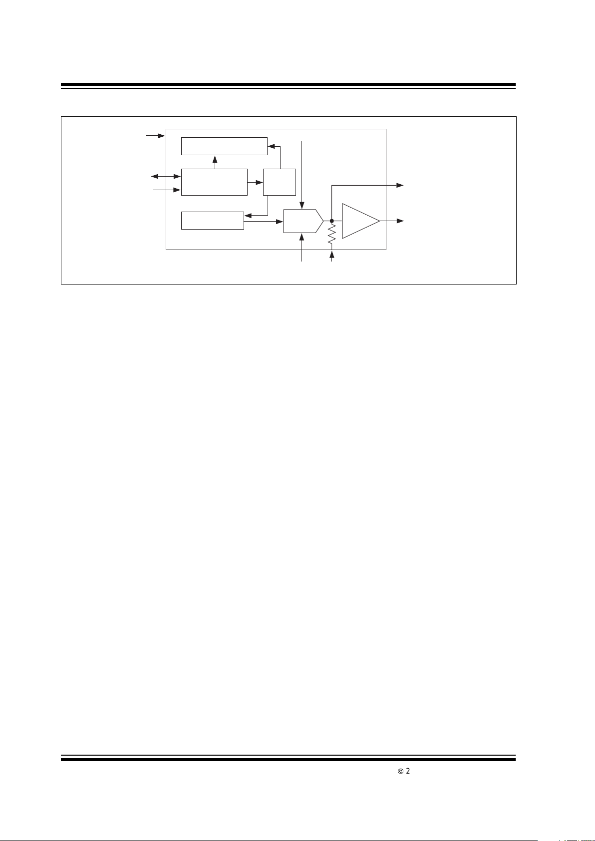
Functional Block Diagram
Serial Port
Interface
SDA
V
DD
DAC-OU
T
V
OUT
Configuration Register
Data Register
Control
V
REF
GND
SCL
DAC
TC1320
2002 Microchip TechnologyInc. DS21386B-page 3
TC1320
1.0 ELECTRICAL
CHARACTERISTICS
Absolute Maximum Ratings*
Supply Voltage (VDD).............................................+6V
Voltage on any Pin..(GND – 0.3V) to (V
DD
+0.3V)
Current on any Pin............................................ ±50mA
Package Thermal Resistance(θ
JA
)............ 330°C C/W
Operating Temperature (T
A
)........................ See Below
StorageTemperature (T
STG
)..............-65°C to +150°C
*Stresses above those listed under "Absolute Maximum
Ratings" may cause permanent damage to the device. These
are stress ratings only and functional operation of the device
at these or any other conditions above those indicated in the
operation sections of the specifications is not implied.
Exposure to Absolute Maximum Rating conditions for
extended periods may affectdevice reliability.
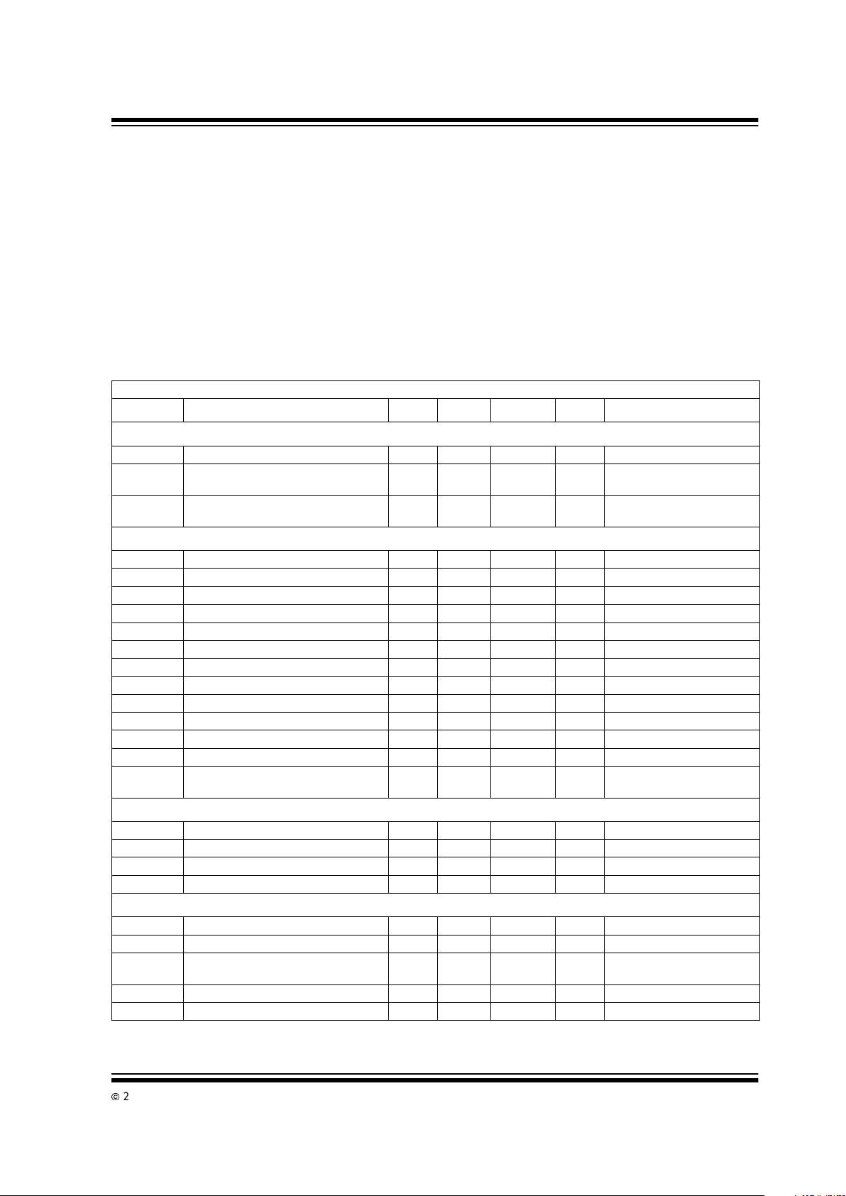
TC1320 ELECTRICAL SPECIFICATIONS
Electrical Characteristics: VDD= 2.7V to 5.5V, -40°C≤ TA≤ +85°C,V
REF
= 1.2V unless otherwise noted.
Symbol Parameter Min Typ Max Unit Test Conditions
Power Supply
V
DD
Supply Voltage 2.7 350 500 µA
I
DD
Operating Current — 0.35 0.5 mA VDD=5.5V,V
REF
=1.2V
Serial Port Inactive (Note 1)
I
DD-STANDBY
Standby SupplyCurrent — 0.1 1 µAVDD=3.3V
Serial Port Inactive (Note 1)
Static Performance - Analog Section
Resolution — — 8 Bits
INL Integral Non-Linearity at FS, T
A
= +25°C — — ±2 LSB (Note 2)
FSE Full Scale Error — — ±3 %FS
DNL Differential Non-Linearity, T
A
= +25°C — — ±0.8 LSB All Codes (Note 2)
V
OS
Offset Error at V
OUT
—±0.3 ±8 mV(Note 2)
TCV
OS
Offset Error Tempco at V
OUT
—10 —µv/°C
PSRR Power Supply Rejection Ratio — 80 — dB V
DD
at DC
V
REF
Voltage Reference Range 0 — VDD–1.2 V
I
REF
Reference Input Leakage Current — — ±1.0 µA
V
SW
Voltage Swing 0 — V
REF
VV
REF
≤ (VDD–1.2V)
R
OUT
Output Resistance @ V
OUT
—5 — Ω R
OUT
(Ω)
I
OUT
Output Current(Source or Sink) — 2 — mA
I
SC
Output Short-Circuit Current
V
DD
=5.5V
—
—
30
20
50
50
mAmASource
Sink
Dynamic Performance
SR VoltageOutputSlewRate — 0.8 — V/µs
t
SETTLE
Output Voltage Full Scale Settling Time — 10 — µsec
t
WU
Wake-up Time — 20 — µs
Digital Feed Through and Crosstalk — 5 — nV-s SDA = V
DD
,SCL=100kHz
Serial Port Interface
V
IH
LogicInputHigh 2.4 — V
DD
V
V
IL
Logic Input Low — — 0.6 —
V
OL
SDA OutputLow —
—
—
—
0.4
0.6
VVIOL= 3mA (Sinking Current)
I
OL
=6mA
C
IN
Input Capacitance SDA, SCL — 5 0.4 pF
I
LEAK
I/O Leakage — — ±1.0 µA
Note 1: SDA and SCL must be connected to V
DD
or GND.
2: Measured at V
OUT
≥ 50mV referredto GND to avoid output buffer clipping.
TC1320
DS21386B-page 4
2002 Microchip TechnologyInc.
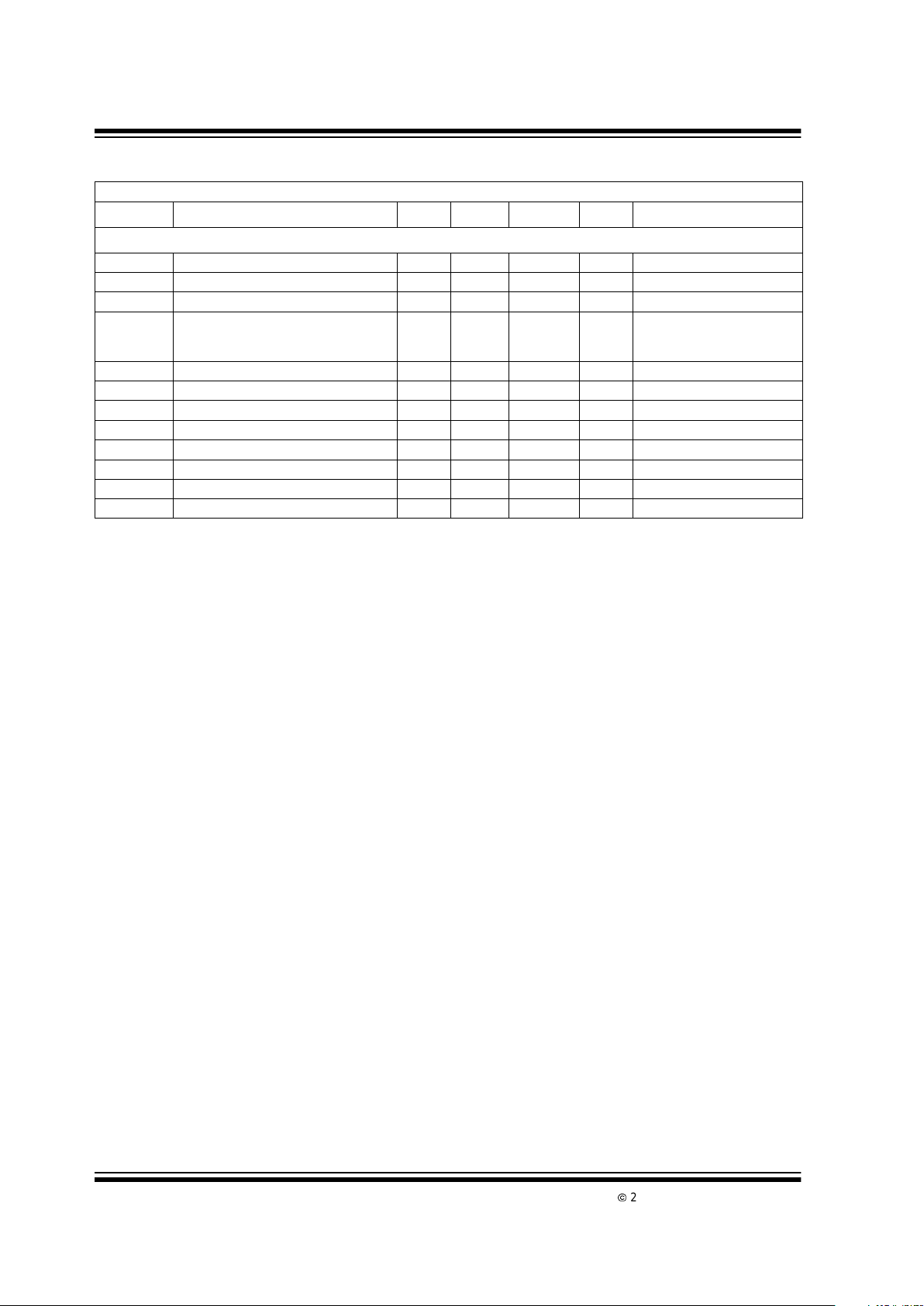
Serial Port AC Timing
f
SMB
SMBus Clock Frequency 10 — 100 kHz
t
IDLE
BusFreeTimePriortoNewTransition 4.7 — — µsec
t
H(START)
START Condition Hold Time 4.0 — — µsec
t
SU(START)
START Condition Setup Time 4.7 — — µsec 90%SCLto10%SDA
(forRepeated START
Condition)
t
SU(STOP)
STOP Condition Setup Time 4.0 — — µsec
t
H-DATA
Data In Hold Time 100 — — nsec
t
SU-DATA
Data In Setup Time 100 — — nsec
t
LOW
Low Clock Period 4.7 — — µsec 10% to 10%
t
HIGH
High Clock Period 4 — — µsec 90% to 90%
t
F
SMBus Fall Time — — 300 nsec 90% to 10%
t
R
SMBusRise Time — — 1000 nsec 10% to 90%
t
POR
Power-on Reset Delay — 500 — µsec VDD ≥ V
POR
(Rising Edge)
TC1320 ELECTRICAL SPECIFICATIONS (CONTINUED)
Electrical Characteristics: VDD= 2.7V to 5.5V, -40°C≤ TA≤ +85°C,V
REF
= 1.2V unless otherwise noted.
Symbol Parameter Min Typ Max Unit Test Conditions
Note 1: SDA and SCL must be connected to V
DD
or GND.
2: Measured at V
OUT
≥ 50mV referredto GND to avoid output buffer clipping.
2002 Microchip TechnologyInc. DS21386B-page 5
TC1320
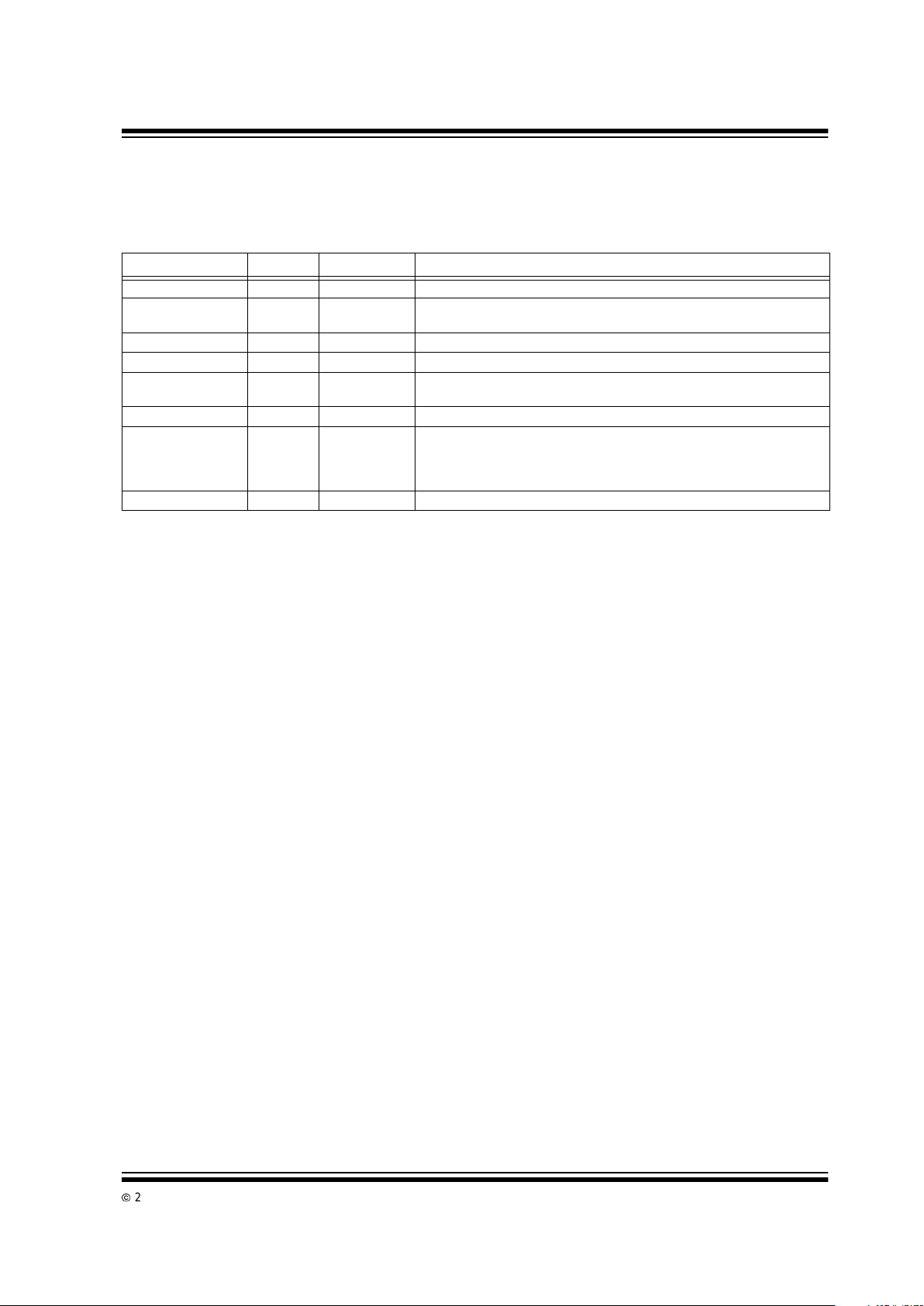
2.0 PIN DESCRIPTIONS
ThedescriptionsofthepinsarelistedinTable2-1.
TABLE 2-1: PIN F UNCTION TABLE
Pin Number Symbol Type Description
1V
REF
Input Input. Voltage Reference Input can range from 0V to 1.2V below VDD.
2 SDA Bi-Directional Bi-directional. Serial data is transferred on the SMBus in both directions
usingthispin.
3 SCL Input Input. SMBus serial clock. Clocks data into and out of the TC1320.
4 GND Power Ground.
5V
OUT
Output Output. Buffered DAC output voltage. This voltage is a function of the
reference voltageandthe contents of the DATA register.
6 NC None No connection.
7 DAC-OUT Output Output. Unbuffered DAC output voltage. This voltage is a function of the
reference voltageandthe contents of the DATA register. This outputis
unbuffered and care must be takenthatthe pin is connected only to a
high-impedancenode.
8V
DD
Power Positive power supply input. See electrical specifications.
 Loading...