

Microchip Technology TC1271RERC, TC1271MERC, TC1271LERC, TC1271FERC, TC1270TERC Datasheet
...
TC1270/TC1271
4-Pin µP Reset Monitors
Features
• PrecisionVCCMonitor for 1.8V, 2.7V, 3.0V, 3. 3V
and 5.0V Nominal Supplies
• Manual Reset Input
• 140msec Mi nimum RESET
, RESET Output
Duration
• RESET
OutputValidtoVCC= 1. 0V (TC1270)
•Low7µA Supply Current
TransientImmunity
•V
CC
• Small 4-Pin SOT-143 Package
• No External Components
• ReplacementforMAX811/812 and Offers a Lower
Threshold Voltage Option
Applications
• Computers
• Embedded Systems
• Battery Powered Equipment
• Critical µP Power Supply Monitoring
Device Selection Table
Part Number Package Temp. Range
TC1270xERC 4-Pin SOT-143 -40°C to +85°C
TC1271xERC 4-Pin SOT-143 -40°C to +85°C
NOTE: “x” denotes a suffix for VCC threshold (see table
below)
Suffix* Reset V
L4.63
M4.38
T3.08
S2.93
R2.63
F1.75
*Custom thresholds available, contact factory.
Threshold (V)
CC
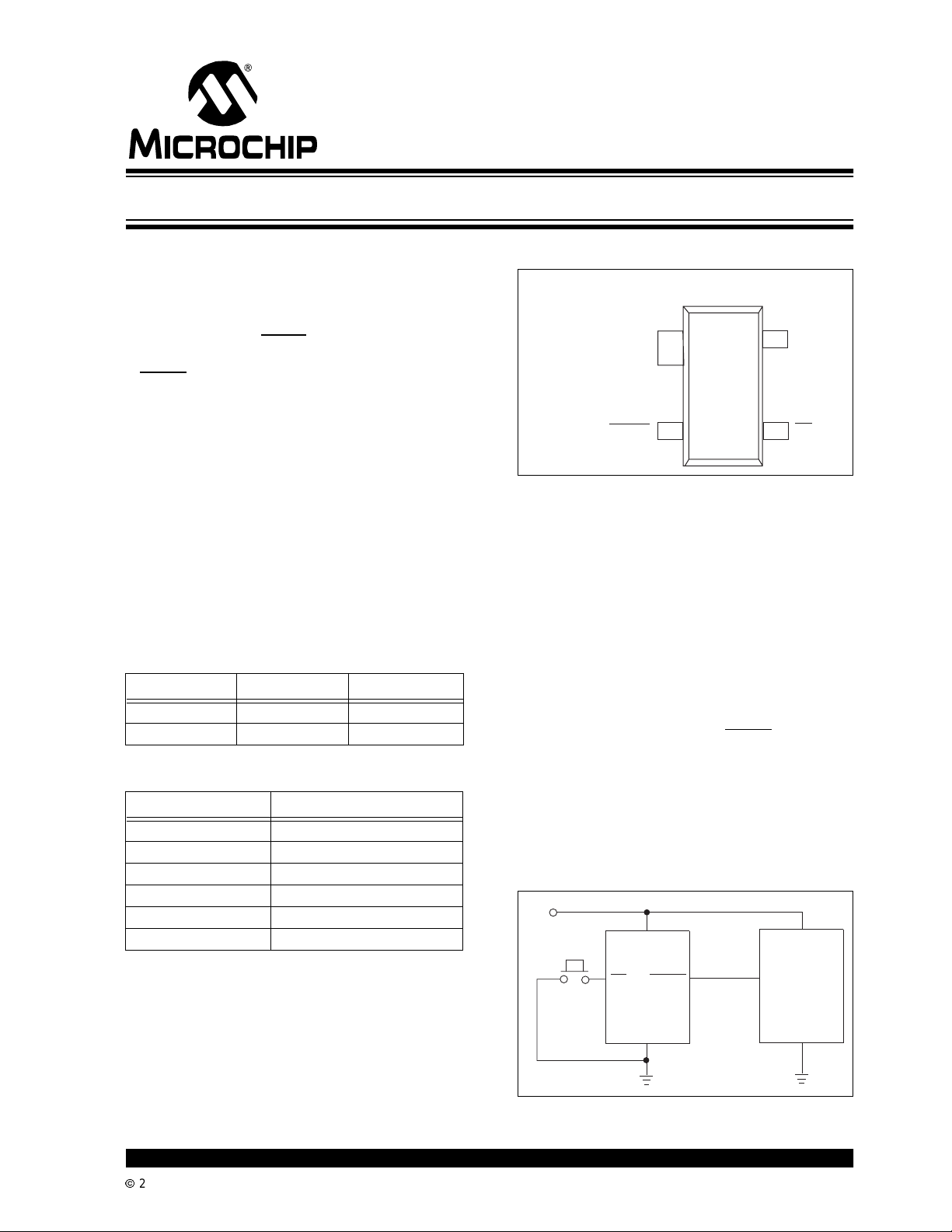
Package Type
4-Pin SOT-143
V
4
GND
1
CC
TC1270
TC1271
TC1270 RESET
TC1271 (RESET)
2
MR
3
General Description
The TC1270 and TC1271 are cost-effective system
supervisor circuits designed to monitor V
CC
in digital
systems and provide a reset signal to the host
processor when necessary. A manual reset input is
provided to override the reset monitor, and is suitable
for use as a push-button reset. No external
components are required.
The reset output is driven active within 20µsec (4µsec
for F version) of V
falling through the reset voltage
CC
threshold. RESET is maintained active for a minimum
of 140msec after V
rises above the reset threshold.
CC
The TC1271 has an active-high RESET output while
the TC1270 has an active-low RESET
output of the TC1270 is valid down to V
output. The
=1V.Both
CC
devices are available in a 4-Pin SOT-143 package.
The TC1270/TC1271 devices are optimized to reject
fast transient glitches on the V
current of 7µA(V
= 3.3V) makes these devices
CC
line. Low supply
CC
suitable for battery powered applications.
Typical Operating Circuit
V
CC
V
CC
Processor
RESET
Input
(Active Low)
Push-
Button
V
CC
MR
RESET
TC1270
GND GND
2002 Microchip TechnologyInc. DS21381B-page 1
TC1270/TC1271
1.0 ELECTRICAL
CHARACTERISTICS
*Stresses above those listed under "Absolute Maximum
Ratings" may cause permanent damage to the device. These
are stress ratings only and functional operation of the device
at these or any other conditions above those indicated in the
Absolute Maximum Ratings*
Supply Voltage (VCCto GND) .............................+6.0V
, RESET..........................-0.3V to (VCC+0.3V)
RESET
Input Current, V
Output Current, RESET
...............................................20mA
CC
, RESET.........................20mA
operation sections of the specifications is not implied.
Exposure to Absolute Maximum Rating conditions for
extended periods may affectdevice reliability.
Operating Temperature Range.............-40°C to +85°C
StorageTemperature Range..............-65°C to +150°C
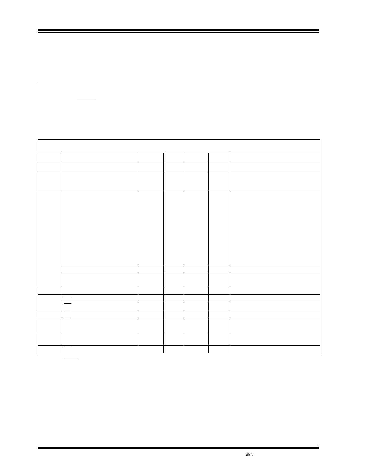
TC1270/TC1271 ELE C TRICAL SPECIFICATIONS
Electrical Characteristics: VCC= 5V for L/M versions, VCC= 3.3V for T/S versions, VCC= 3V for R version,VCC=2.0VforF
version. T
Symbol Parameter Min Typ Max Units Test Conditions
V
CC
I
CC
V
TH
t
RP
t
MR
t
MD
V
IH
V
IL
V
IH
V
IL
Note 1: Production testing done at TA= +25°C, over temperature limits ensured by design.
= -40°C to +85°C unless otherwise noted. Typical values are at TA=+25°C.(Note1).
A
VCCRange 1.2 — 5.5 V
Supply Current —
—
—
Reset Threshold 4.54
4.50
4.30
4.25
3.03
3.00
2.88
2.85
2.58
2.55
1.71
1.70
7
10
6
4.63
—
4.38
—
3.08
—
2.93
—
2.63
—
1.75
—
15
15
12
4.72
4.75
4.46
4.50
3.14
3.15
2.98
3.00
2.68
2.70
1.79
1.80
µAV
V TC127_L; T
Reset Threshold Tempco — 30 — ppm/°C
to Reset Delay —
V
CC
—
20
5
—
—
µsec VCC=VTHto VTH– 125mV; L/M/R/S/T/F
Reset Active Timeout Period 140 280 560 msec VCC=V
MR Minimum Pulse Width 10 — — µsec
Glitch Immunity — 0.1 — µsec
MR
MR to Reset Propagation Delay — 0.5 — µsec
MR Input Threshold 2.3
—
0.7 V
—
Pull-upResistance 10 20 40 kΩ
MR
2: RESET
output for TC1270, RESET output for TC1271.
CC
—
—
—
0.8
—
——0.15 V
VVCC>V
VVCC>V
CC
CC>VTH
V
CC<VTH
V
CC<VTH
T
A
TC127_M; T
T
A
TC127_T; T
T
A
TC127_S; T
T
A
TC127_R; T
T
A
TC127_F; T
T
A
, for L/M/R/S/T/F
, for L/M/R/S/T
,forF
= -40°C to +85°C
A
= -40°C to +85°C
= -40°C to +85°C
A
A
A
= -40°C to +85°C
= -40°C to +85°C
= -40°C to +85°C
A
A
TH(MAX)
TH(MAX)
TC127_L/M
TH(MAX)
TC127_R/S/T/F
=+25°C
=+25°C
=+25°C
=+25°C
=+25°C
=+25°C
,
,
DS21381B-page 2
2002 Microchip TechnologyInc.
TC1270/TC1271
TC1270/TC1271 ELE C TRICAL SPECIFICATIONS (CONTINUED)
Electrical Characteristics: VCC= 5V for L/M versions, VCC=3.3VforT/Sversions,VCC= 3V for R version, VCC=2.0VforF
version.T
Symbol Parameter Min Typ Max Units Test Conditions
V
OH
V
OL
V
OL
V
OH
= -40°C to +85°C unless otherwisenoted. Typical values are at TA= +25°C. (Note 1).
A
RESET Output Voltage High
(TC1271)
RESET Output Voltage Low
(TC1271) —
0.8 V
—— VI
CC
—
0.2
V
V TC1271F only,
I
V
TC1271R/S/T only,
—
—
—
—
0.3
0.4
I
TC1271L/M only, I
V
RESET Output Voltage Low
(TC1270)
—
—
0.3
V TC1270R/S/T only,
I
TC1270F only:
I
TC1270L/M only,
I
I
V TC1270L/M only,
I
RESET Output Voltage High
(TC1270)
—
—
VCC–1.5
—
—
—
0.4
TBD
—
V
=150µA;
SOURCE
≤ V
CC
TH(MIN)
=500µA,
SINK
CC=VTH(MAX)
=1.2mA,VCC=V
SINK
CC=VTH(MAX)
=1.2mA,VCC=V
SINK
=500µA, VCC=V
SINK
=3.2mA,VCC=V
SINK
=50µA, VCC>1.0V
SINK
=800µA,
SOURCE
CC=VTH(MAX)
SINK
TH(MAX)
=3.2mA,
TH(MIN)
TH(MIN)
TH(MIN)
0.8 V
Note 1: Production testing done at TA= +25°C, over temperature limits ensured by design.
2: RESET
output for TC1270, RESET output for TC1271.
CC
—
—
TC1270R/S/T/Fonly,
I
V
=500µA,
SOURCE
CC=VTH(MAX)
2002 Microchip TechnologyInc. DS21381B-page 3
TC1270/TC1271
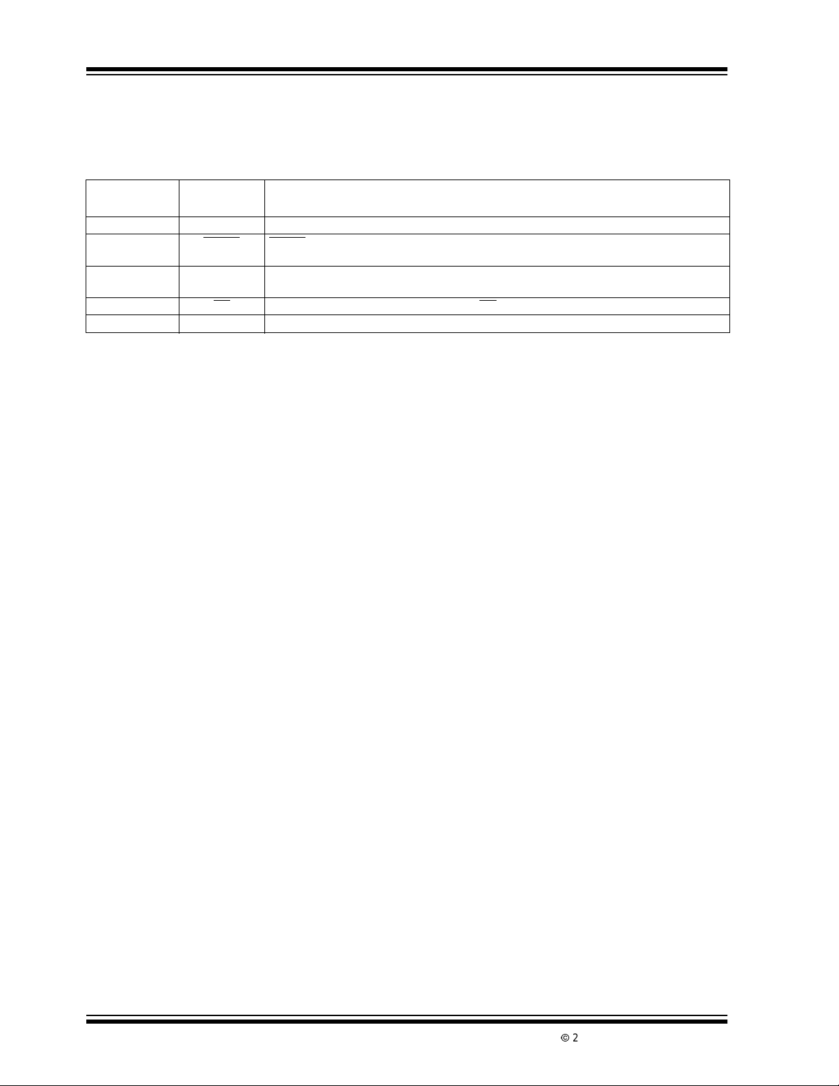
2.0 PIN DESCRIPTIONS
ThedescriptionsofthepinsarelistedinTable2-1.
TABLE 2-1: PIN FUNCTION TABLE
Pin No.
(SOT-143-4)
1 GND Ground.
2 RESET
2 RESET
3MR
4V
Symbol Description
(TC1270)
(TC1271)
CC
outputremains low while VCCis below the reset voltage threshold,andfor at least
RESET
140msec min. after V
RESET output remains high while V
140msec min. after V
Manual reset input generates a reset when MR is belowVIL.
Supply voltage.
risesabove reset threshold.
CC
is below the reset voltage threshold,andfor at least
risesabove reset threshold.
CC
CC
DS21381B-page 4
2002 Microchip TechnologyInc.
 Loading...