

Datasheet TC1271RERC, TC1271MERC, TC1271LERC, TC1271FERC, TC1270TERC Datasheet (Microchip Technology)
...
TC1270/TC1271
4-Pin µP Reset Monitors
Features
• PrecisionVCCMonitor for 1.8V, 2.7V, 3.0V, 3. 3V
and 5.0V Nominal Supplies
• Manual Reset Input
• 140msec Mi nimum RESET
, RESET Output
Duration
• RESET
OutputValidtoVCC= 1. 0V (TC1270)
•Low7µA Supply Current
TransientImmunity
•V
CC
• Small 4-Pin SOT-143 Package
• No External Components
• ReplacementforMAX811/812 and Offers a Lower
Threshold Voltage Option
Applications
• Computers
• Embedded Systems
• Battery Powered Equipment
• Critical µP Power Supply Monitoring
Device Selection Table
Part Number Package Temp. Range
TC1270xERC 4-Pin SOT-143 -40°C to +85°C
TC1271xERC 4-Pin SOT-143 -40°C to +85°C
NOTE: “x” denotes a suffix for VCC threshold (see table
below)
Suffix* Reset V
L4.63
M4.38
T3.08
S2.93
R2.63
F1.75
*Custom thresholds available, contact factory.
Threshold (V)
CC
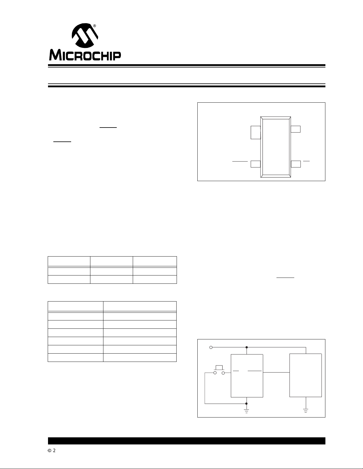
Package Type
4-Pin SOT-143
V
4
GND
1
CC
TC1270
TC1271
TC1270 RESET
TC1271 (RESET)
2
MR
3
General Description
The TC1270 and TC1271 are cost-effective system
supervisor circuits designed to monitor V
CC
in digital
systems and provide a reset signal to the host
processor when necessary. A manual reset input is
provided to override the reset monitor, and is suitable
for use as a push-button reset. No external
components are required.
The reset output is driven active within 20µsec (4µsec
for F version) of V
falling through the reset voltage
CC
threshold. RESET is maintained active for a minimum
of 140msec after V
rises above the reset threshold.
CC
The TC1271 has an active-high RESET output while
the TC1270 has an active-low RESET
output of the TC1270 is valid down to V
output. The
=1V.Both
CC
devices are available in a 4-Pin SOT-143 package.
The TC1270/TC1271 devices are optimized to reject
fast transient glitches on the V
current of 7µA(V
= 3.3V) makes these devices
CC
line. Low supply
CC
suitable for battery powered applications.
Typical Operating Circuit
V
CC
V
CC
Processor
RESET
Input
(Active Low)
Push-
Button
V
CC
MR
RESET
TC1270
GND GND
2002 Microchip TechnologyInc. DS21381B-page 1
TC1270/TC1271
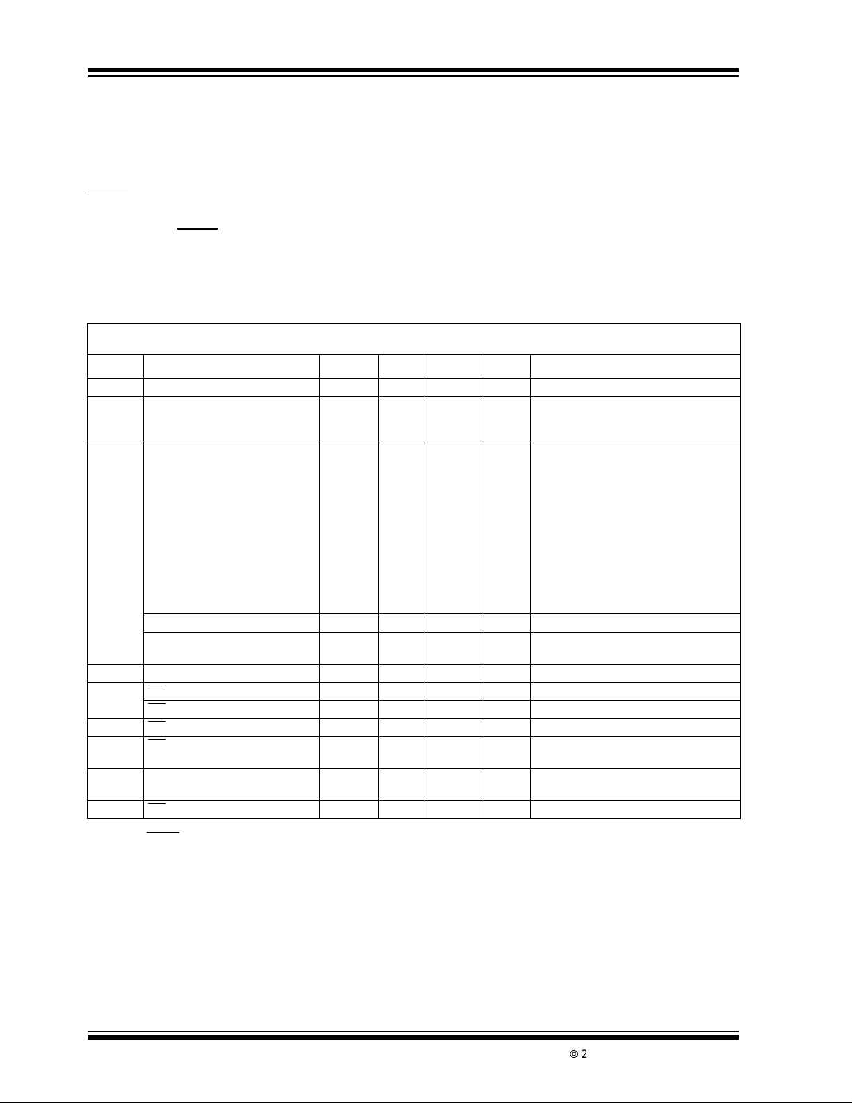
1.0 ELECTRICAL
CHARACTERISTICS
*Stresses above those listed under "Absolute Maximum
Ratings" may cause permanent damage to the device. These
are stress ratings only and functional operation of the device
at these or any other conditions above those indicated in the
Absolute Maximum Ratings*
Supply Voltage (VCCto GND) .............................+6.0V
, RESET..........................-0.3V to (VCC+0.3V)
RESET
Input Current, V
Output Current, RESET
...............................................20mA
CC
, RESET.........................20mA
operation sections of the specifications is not implied.
Exposure to Absolute Maximum Rating conditions for
extended periods may affectdevice reliability.
Operating Temperature Range.............-40°C to +85°C
StorageTemperature Range..............-65°C to +150°C
TC1270/TC1271 ELE C TRICAL SPECIFICATIONS
Electrical Characteristics: VCC= 5V for L/M versions, VCC= 3.3V for T/S versions, VCC= 3V for R version,VCC=2.0VforF
version. T
Symbol Parameter Min Typ Max Units Test Conditions
V
CC
I
CC
V
TH
t
RP
t
MR
t
MD
V
IH
V
IL
V
IH
V
IL
Note 1: Production testing done at TA= +25°C, over temperature limits ensured by design.
= -40°C to +85°C unless otherwise noted. Typical values are at TA=+25°C.(Note1).
A
VCCRange 1.2 — 5.5 V
Supply Current —
—
—
Reset Threshold 4.54
4.50
4.30
4.25
3.03
3.00
2.88
2.85
2.58
2.55
1.71
1.70
7
10
6
4.63
—
4.38
—
3.08
—
2.93
—
2.63
—
1.75
—
15
15
12
4.72
4.75
4.46
4.50
3.14
3.15
2.98
3.00
2.68
2.70
1.79
1.80
µAV
V TC127_L; T
Reset Threshold Tempco — 30 — ppm/°C
to Reset Delay —
V
CC
—
20
5
—
—
µsec VCC=VTHto VTH– 125mV; L/M/R/S/T/F
Reset Active Timeout Period 140 280 560 msec VCC=V
MR Minimum Pulse Width 10 — — µsec
Glitch Immunity — 0.1 — µsec
MR
MR to Reset Propagation Delay — 0.5 — µsec
MR Input Threshold 2.3
—
0.7 V
—
Pull-upResistance 10 20 40 kΩ
MR
2: RESET
output for TC1270, RESET output for TC1271.
CC
—
—
—
0.8
—
——0.15 V
VVCC>V
VVCC>V
CC
CC>VTH
V
CC<VTH
V
CC<VTH
T
A
TC127_M; T
T
A
TC127_T; T
T
A
TC127_S; T
T
A
TC127_R; T
T
A
TC127_F; T
T
A
, for L/M/R/S/T/F
, for L/M/R/S/T
,forF
= -40°C to +85°C
A
= -40°C to +85°C
= -40°C to +85°C
A
A
A
= -40°C to +85°C
= -40°C to +85°C
= -40°C to +85°C
A
A
TH(MAX)
TH(MAX)
TC127_L/M
TH(MAX)
TC127_R/S/T/F
=+25°C
=+25°C
=+25°C
=+25°C
=+25°C
=+25°C
,
,
DS21381B-page 2
2002 Microchip TechnologyInc.
TC1270/TC1271
TC1270/TC1271 ELE C TRICAL SPECIFICATIONS (CONTINUED)
Electrical Characteristics: VCC= 5V for L/M versions, VCC=3.3VforT/Sversions,VCC= 3V for R version, VCC=2.0VforF
version.T
Symbol Parameter Min Typ Max Units Test Conditions
V
OH
V
OL
V
OL
V
OH
= -40°C to +85°C unless otherwisenoted. Typical values are at TA= +25°C. (Note 1).
A
RESET Output Voltage High
(TC1271)
RESET Output Voltage Low
(TC1271) —
0.8 V
—— VI
CC
—
0.2
V
V TC1271F only,
I
V
TC1271R/S/T only,
—
—
—
—
0.3
0.4
I
TC1271L/M only, I
V
RESET Output Voltage Low
(TC1270)
—
—
0.3
V TC1270R/S/T only,
I
TC1270F only:
I
TC1270L/M only,
I
I
V TC1270L/M only,
I
RESET Output Voltage High
(TC1270)
—
—
VCC–1.5
—
—
—
0.4
TBD
—
V
=150µA;
SOURCE
≤ V
CC
TH(MIN)
=500µA,
SINK
CC=VTH(MAX)
=1.2mA,VCC=V
SINK
CC=VTH(MAX)
=1.2mA,VCC=V
SINK
=500µA, VCC=V
SINK
=3.2mA,VCC=V
SINK
=50µA, VCC>1.0V
SINK
=800µA,
SOURCE
CC=VTH(MAX)
SINK
TH(MAX)
=3.2mA,
TH(MIN)
TH(MIN)
TH(MIN)
0.8 V
Note 1: Production testing done at TA= +25°C, over temperature limits ensured by design.
2: RESET
output for TC1270, RESET output for TC1271.
CC
—
—
TC1270R/S/T/Fonly,
I
V
=500µA,
SOURCE
CC=VTH(MAX)
2002 Microchip TechnologyInc. DS21381B-page 3
TC1270/TC1271
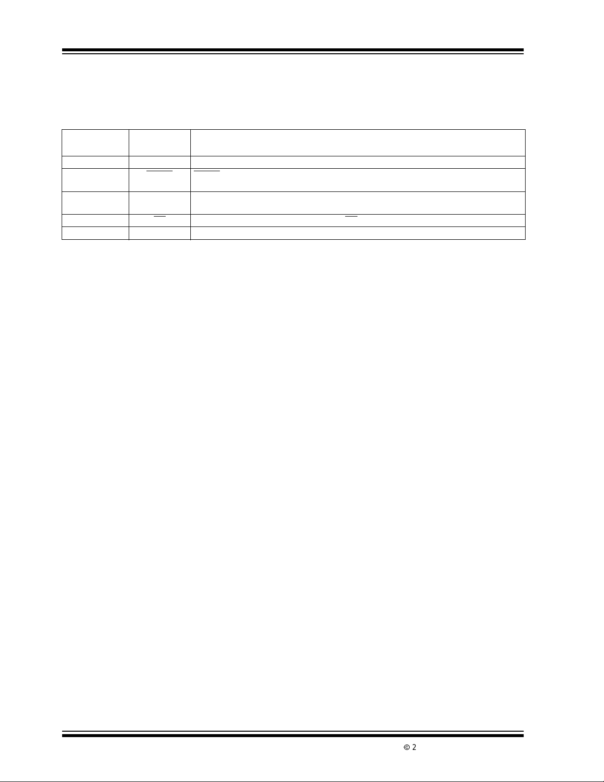
2.0 PIN DESCRIPTIONS
ThedescriptionsofthepinsarelistedinTable2-1.
TABLE 2-1: PIN FUNCTION TABLE
Pin No.
(SOT-143-4)
1 GND Ground.
2 RESET
2 RESET
3MR
4V
Symbol Description
(TC1270)
(TC1271)
CC
outputremains low while VCCis below the reset voltage threshold,andfor at least
RESET
140msec min. after V
RESET output remains high while V
140msec min. after V
Manual reset input generates a reset when MR is belowVIL.
Supply voltage.
risesabove reset threshold.
CC
is below the reset voltage threshold,andfor at least
risesabove reset threshold.
CC
CC
DS21381B-page 4
2002 Microchip TechnologyInc.

TC1270/TC1271
,
V
V
CC
)
00
0
60
320
80
0
1
0
0
000
(
C
n
O
e
J
/S/T
3.0 APPLICATIONS INFORMATION
3.1 VCCTransient Rejection
The TC1270/TC1271 provides accurate VCCmonitoringand resettimingduringpower-up,power-down, and
brownout/sag conditions, and rejects negative-going
transients (glitches) on the power supply line. Figure
3-1 shows the maximum transient duration vs.
maximum negative excursion (overdrive) for glitch
rejection. Any combination of duration and overdrive
that l ays under the curve will not generate a reset
signal. Combinations above the curve are detected as
a brownout or power-down. Transientimmunity can be
improvedbyaddingacapacitor in close proximitytothe
V
pin of the TC1270/TC1271.
CC
FIGURE 3-1: MAXIMUM TRANSIENT
DURATION VS.
OVERDRIVE FOR GLITCH
REJECTION AT 25°C
V
CC
V
TH
verdriv
beconnectedfromRESET
togroundtodischargestray
capacitances and hold the output low(Figure 3-2). This
resistor value, though not critical, should be chosen
such that it does not appreciably load RESET
under
normal operation (100kΩ will be suitable for most
applications). Similarly, a pull-up r esistor t o V
CC
required for the TC1271 to ensure a valid high RESET
for VCCbelow 1.1V.
FIGURE 3-2: ENSURING RESET VALID
TO V
V
CC
V
CC
CC
=0V
TC1270
RESET
R1
GND
100k
3.3 Processors With Bidirectional
I/O Pins
is
Some µP' s (such as Motorola 68HC11) have bi-
Duratio
4
directional reset pins. Depending on the current drive
capability of the processor pin, an indeterminate logic
level may result if there is a logic conflict. This can be
avoided by adding a 4.7 kΩ resistor in series with the
output of the TC1270/TC1271 (Figure 3-3). If there are
other components in the system which require a reset
24
signal, they should be buffered so as not to load the
reset line. If the other components are required to
1
TC127LM
follow the reset I/O of the µP, the buffer should be
connected as shown with the solid line.
FIGURE 3-3: INTERFACING TO
AXIMUM TRANSIENT DURATION
3.2 RESET Signal Integrity During
The TC1270 RESET output is valid to VCC=1.0V.
Below this voltage the output becomes an "open
circuit" and does not sink current. This means CMOS
logic inputs to the µPwillbefloatingatan
TC127xR
1
RESET COMPARATOR OVERDRIVE
10
-
(mV
Power-Down
1
V
CC
V
CC
TC1270
RESET
GND
undetermined voltage. Most digital systems are
completely shut down well above this voltage.
However, in situations where RESET
maintained valid to V
= 0V,a pull-down resistor must
CC
must b e
BIDIRECTIONAL
RESET I/O
Buffer
V
CC
4.7k
µP
RESET
GND
Buffered RESET
To Other System
Components
2002 Microchip TechnologyInc. DS21381B-page 5

TC1270/TC1271
CC
)
8
0
6
0
0
020
0406085
(
e
(
)
CC
= 5V
CC
= 3V
)
30
0
50
0
0
0
0
0
0
040
60
85
e
(
)
OD
V
OD
V
OD
V
)
0
5
50
35
30
5
0
0
0
040
60
85
e
/M
/S/T/F
8
6
0
)
0
020
0406085
e
(
)
V
CC
5V
CC
3V
V
CC
1V
/M
R/S/T
)
30
0
50
010
0
0
0
0
040
60
85
e
(
)
V
O
= 20
OD
V
OD
V
OD
V
V
OD
V
OD
V
0
0
0030
0000
0.9990
0.9980
0.9970
0.9960
0.9950
0.9940
)
0
0
35
5
65
60
e
4.0 TYPICAL CHARACTERISTICS
Note: The graphs and tables provided following this note are a statisticalsummary based on a limited number of
samplesandareprovidedforinformational purposesonly. The performance characteristics listed hereinare
not tested or guaranteed. In some graphs or tables, the datapresented may be outside the specified
operating range ( e.g., outside specified power supply range) and therefore outside the warranted range.
Supply Current vs.Temperatur
No Load, TC127xR/S/T/F
A
1
UPPLY CURRENT
-4
-2
TEMPERATURE (C
Power-Down Reset Delay vs. Temperatur
TC127xF
4
2
1
POWER-DOWN RESET DELAY (µsec)
= 200 m
-4
-2
2
TEMPERATURE (C
=
= 20m
= 100m
Supply Current vs.Temperatur
No Load, TC127xL/M
=
=
SUPPLY CURRENT (µA)
-4
-2
TEMPERATURE (C
Power-Down Reset Delay vs. Temperatur
TC127xL/M/R/S/T
POWER-DOWN RESET DELAY (µsec)
L
4
2
-4
= 200m
-2
= 100m
= 100m
2
TEMPERATURE (C
=
= 200m
= 20m
Power-Up Reset Timeout vs. Temperatur
2
24
24
2
2
POWER-UP RESET TIMEOUT (msec)
22
-4
-2
TEMPERATURE (C
2
TC127xL
TC127xR
DS21381B-page 6
Normalized Reset Threshold vs. Temperatur
1.
1.002
1.001
1.
NORMALIZED THRESHOLD (V)
-4
-1
1
TEMPERATURE (C
2002 Microchip TechnologyInc.

TC1270/TC1271
)
)
)
)
)
)
)
)
)
)
)
)
)
)
)
)
)
)
)
)
)
)
8
3
5.0 PACKAGING INFORMATION
5.1 Package Marking Information
1
2
& = part number code + temperature range
(two-digit code)
Part Number (V) Code
TC1270LERC 4.63 S1
TC1270MERC 4.38 S2
TC1270TERC 3.08 S3
TC1270SERC 2.93 S4
TC1270RERC 2.63 S5
TC1270FERC 1.75 S7
5.2 Package Dimensions
4-Pin SOT-14
.079 (2.00
.071 (1.80
PartNumber (V) Code
TC1271LERC 4.63 T1
TC1271MERC 4.38 T2
TC1271TERC 3.08 T3
TC1271SERC 2.93 T4
TC1271RERC 2.63 T5
TC1271FERC 1.75 T7
3
represents year and quarter code
4
represents production lot ID code
.040 (1.02
.031 (0.79
.004 (0.10
.001(0.02
.098 (2.50
.083 (2.10
.080 (2.03
.070 (1.78
.120 (3.05
.105 (2.67
.037 (0.94
.030 (0.77
.021 (0.54
.015 (0.38
.055 (1.40
.047 (1.20
.006 (0.15
.004 (0.09
.010 (0.25
.005 (0.13
Dimensions: inches (mm)
2002 Microchip TechnologyInc. DS21381B-page 7

TC1270/TC1271
NOTES:
DS21381B-page 8
2002 Microchip TechnologyInc.

TC1270/TC1271
Sales and Support
Data Sheets
Products supportedby a preliminary Data Sheet may have an errata sheet describing minor operational differences and recommendedworkarounds.To determine if an errata sheet exists for a particulardevice, please contactone of the following:
1. Yo ur local Microchip sales office
2. The Microchip Corporate Literature Center U.S. FAX:(480) 792-7277
3. The Microchip Worldwide Site (www.microchip.com)
Pleasespecify which device, revision of silicon and Data Sheet (includeLiterature #) you are using.
New Customer Notification System
Register on our web site (www.microchip.com/cn) to receive the most current information on our products.
2002 Microchip Technology Inc. DS21381B-page9

TC1270/TC1271
NOTES:
DS21381B-page10 2002 Microchip Technology Inc.

TC1270/TC1271
Information contained in this publication regarding device
applications and the like is intended through suggestion only
and may be superseded by updates. It is your responsibility to
ensure that your application meets with your specifications.
No representation or warranty is given and no liability is
assumed by Microchip Technology Incorporated with respect
to the accuracy or use of such information, or infringement of
patents or other intellectual property rights arising from such
use or otherwise. Use of Microchip’s products as critical components in life support systems is not authorized except with
express written approval by Microchip. No licenses are conveyed, implicitly or otherwise, under any intellectual property
rights.
Trademarks
The Microchip name and logo, the Microchip logo, FilterLab,
K
EELOQ,microID,MPLAB,PIC,PICmicro,PICMASTER,
PICSTART, PRO MATE, SEEV A L and The Embedded Control
SolutionsCompany areregiste red trademarksof MicrochipTechnologyIncorp or ated in the U.S.A. and other countries .
dsPIC, ECONOMONITOR, FanSense, FlexROM, fuzzyLAB,
In-Circuit Serial Programming, ICSP, ICEPIC, microPort,
Migratable Memory, MPA SM, MPLIB, MPLINK, MPSIM,
MXDEV,MXLAB, PICC, PICDEM, PICDEM.net, rfPIC, Select
Mode and Total Endurance are trademarks of Microchip
TechnologyIncorporated in the U.S.A.
Serialized Quick Turn Programming (SQTP) is a service mark
of Microchip TechnologyIncorporated in t he U.S.A.
All other trademarks mentioned herein are property of their
respective companies.
© 2002, Microchip Technology Incorporated, Printed in the
U.S.A., All Rights Reserve d.
Printed on recycled paper.
Microchip received QS-9000 quality system
certification for its worldwide headquarters,
design and wafer fabrication facilities in
Chandler and Tempe, Arizona in July 1999
and Mountain View, California in March 2002.
The Company’s quality system processes and
procedures are QS-9000 compliant for its
®
PICmicro
devices, Serial EEPROMs, microperipherals,
non-volatile memory and analog products. In
addition, Microchip’s quality system for the
design and manufacture of development
systemsisISO 9001certified.
2002 Microchip TechnologyInc. DS21381B-page 11
8-bit MCUs, KEELOQ®code hopping

WORLDWIDE SALES AND SERVICE
AMERICAS
Corporate Office
2355 West Chandler Blvd.
Chandler, AZ 85224-6199
Tel: 480-792-7200 Fax: 480-792-7277
Technical Support: 480-792-7627
Web Address: http://www.microchip.com
Rocky Mountain
2355 West Chandler Blvd.
Chandler, AZ 85224-6199
Tel: 480-792-7966 Fax: 480-792-7456
Atlanta
500 Sugar Mill Road, Suite 200B
Atlanta, GA 30350
Tel: 770-640-0034 Fax: 770-640-0307
Boston
2 Lan Drive, Suite 120
Westford, MA 01886
Tel: 978-692-3848 Fax: 978-692-3821
Chicago
333 Pierce Road, Suite 180
Itasca, IL 60143
Tel: 630-285-0071 Fax: 630-285-0075
Dallas
4570 Westgrove Drive, Suite 160
Addison, TX 75001
Tel: 972-818-7423 Fax: 972-818-2924
Detroit
Tri-Atria Office Building
32255 Northwestern Highway, Suite 190
Farmington Hills, MI 48334
Tel: 248-538-2250 Fax: 248-538-2260
Kokomo
2767 S. Albright Road
Kokomo, Indiana 46902
Tel: 765-864-8360 Fax: 765-864-8387
Los Angeles
18201 Von Karman, Suite 1090
Irvine, CA 92612
Tel: 949-263-1888 Fax: 949-263-1338
New York
150 Motor Parkway, Suite 202
Hauppauge, NY 11788
Tel: 631-273-5305 Fax: 631-273-5335
San Jose
Microchip Technology Inc.
2107 North First Street, Suite 590
San Jose, CA 95131
Tel: 408-436-7950 Fax: 408-436-7955
Toronto
6285 Northam Drive, Suite 108
Mississauga, Ontario L4V 1X5, Canada
Tel: 905-673-0699 Fax: 905-673-6509
ASIA/PACIFIC
Australia
Microchip Technology Australia Pty Ltd
Suite 22, 41 Rawson Street
Epping 2121, NSW
Australia
Tel: 61-2-9868-6733 Fax: 61-2-9868-6755
China - Beijing
Microchip Technology Consulting (Shanghai)
Co., Ltd., Beijing Liaison Office
Unit 915
Bei Hai Wan Tai Bldg.
No. 6 Chaoyangmen Beidajie
Beijing, 100027, No. China
Tel: 86-10-85282100 Fax: 86-10-85282104
China - Chengdu
Microchip Technology Consulting (Shanghai)
Co., Ltd., Chengdu Liaison Office
Rm. 2401, 24th Floor,
Ming Xing Financial Tower
No. 88 TIDU Street
Chengdu 610016, China
Tel: 86-28-86766200 Fax: 86-28-86766599
China - Fuzhou
Microchip Technology Consulting (Shanghai)
Co., Ltd., Fuzhou Liaison Office
Unit 28F, World Trade Plaza
No. 71 Wusi Road
Fuzhou 350001, China
Tel: 86-591-7503506 Fax: 86-591-7503521
China - Shanghai
Microchip Technology Consulting (Shanghai)
Co., Ltd.
Room 701, Bldg. B
Far East International Plaza
No. 317 Xian Xia Road
Shanghai, 200051
Tel: 86-21-6275-5700 Fax: 86-21-6275-5060
China - Shenzhen
Microchip Technology Consulting (Shanghai)
Co., Ltd., Shenzhen Liaison Office
Rm. 1315, 13/F , Shenzhen Kerry Centre,
Renminnan Lu
Shenzhen 518001, China
Tel: 86-755-2350361 Fax: 86-755-2366086
China - Hong K ong SAR
Microchip Technology Hongkong Ltd.
Unit 901-6, Tower 2, Metroplaza
223 Hing Fong Road
Kwai Fong, N.T., Hong Kong
Tel: 852-2401-1200 Fax: 852-2401-3431
India
Microchip Technology Inc.
India Liaison Office
Divyasree Chambers
1 Floor, Wing A (A3/A4)
No. 11, O’Shaugnessey Road
Bangalore, 560 025, India
Tel: 91-80-2290061 Fax: 91-80-2290062
Japan
Microchip Technology Japan K.K.
Benex S-1 6F
3-18-20, Shinyokohama
Kohoku-Ku, Yokohama-shi
Kanagawa, 222-0033, Japan
Tel: 81-45-471- 6166 Fax: 81-45-471-6122
Korea
Microchip Technology Korea
168-1, Youngbo Bldg. 3 Floor
Samsung-Dong, Kangnam-Ku
Seoul, Korea 135-882
Tel: 82-2-554-7200 Fax: 82-2-558-5934
Singapore
Microchip Technology Singapore Pte Ltd.
200 Middle Road
#07-02 Prime Centre
Singapore, 188980
Tel: 65-6334-8870 Fax: 65-6334-8850
Taiwan
Microchip Technology Taiwan
11F-3, No. 207
Tung HuaNorth Road
Taipei, 105, Taiwan
Tel: 886-2-2717-7175 Fax: 886-2-2545-0139
EUROPE
Denmark
Microchip Technology Nordic ApS
Regus Business Centre
Lautrup hoj 1-3
Ballerup DK-2750 Denmark
Tel: 45 4420 9895 Fax: 45 4420 9910
France
Microchip Technology SARL
Parc d’Activite du Moulin de Massy
43 Rue du Saule Trapu
Batiment A - ler Etage
91300 Massy, France
Tel: 33-1-69-53-63-20 Fax: 33-1-69-30-90-79
Germany
Microchip Technology GmbH
Gustav-Heinemann Ring 125
D-81739 Munich, Germany
Tel: 49-89-627-144 0 Fax: 49-89-627-144-44
Italy
Microchip Technology SRL
Centro Direzionale Colleoni
Palazzo Taurus 1 V. Le Colleoni 1
20041 Agrate Brianza
Milan, Italy
Tel: 39-039-65791-1 Fax: 39-039-6899883
United Kingdom
Microchip Ltd.
505 Eskdale Road
Winnersh Triangle
Wokingham
Berkshire, England RG415TU
Tel: 44 118 921 5869 Fax: 44-118921-5820
05/01/02
DS21381B-page 12
2002 Microchip Technology Inc.
 Loading...