

Page 1

AN5365
SAM L11 Security Reference Guide
Introduction
This document is intended to help the developer to use SAM L11 security features for building secure
embedded applications.
The following application development aspects are covered in this document:
• Single and dual developer approach
• Secure solution development using SAM L11 ecosystem
• Secure software protection using ARM® TrustZone® for cortex®-M and Debug Access Levels
• System root of trust using Secure boot
The use of key security features is illustrated using bare-metal software examples on the following:
• Using SAM L11 Secure, Non-Secure, and Mix Secured peripherals.
• Using an embedded Cryptographic Accelerator (CRYA) for AES-128, SHA-256, and GCM algorithm.
• Using Data Flash and Trust RAM for storing and protecting application secrets using tamper
detection, scrambling, and silent accesses.
© 2019 Microchip Technology Inc.
DS70005365B-page 1
Page 2

AN5365
Table of Contents
Introduction......................................................................................................................1
1. Introduction to SAM L11 Security Features............................................................... 3
1.1. TrustZone for ARMv8-M ..............................................................................................................3
1.2. Secure and Non-Secure Peripherals............................................................................................9
1.3. Mix-Secure Integrated Peripherals.............................................................................................10
1.4. Debug Access Level (DAL) and Chip Erase.............................................................................. 13
1.5. Secure Boot................................................................................................................................17
2. SAM L11 Application Development (Customer A and Customer B)........................21
2.1. Single-Developer Approach....................................................................................................... 21
2.2. Dual-Developer Approach.......................................................................................................... 21
2.3. Develop a Secure Solution (Customer A).................................................................................. 22
2.4. Develop a Non-Secure Project (Customer B)............................................................................ 40
2.5. Developing Solution with Secure Boot Program (Customer A).................................................. 56
3. Software Use Case Examples.................................................................................66
3.1. Non-Secure Peripheral (TC0).....................................................................................................66
3.2. Secure Peripheral (TC0)............................................................................................................ 68
3.3. Mix-Secure Peripheral (EIC)...................................................................................................... 70
3.4. TrustRAM................................................................................................................................... 74
3.5. Cryptographic Accelerator (CRYA).............................................................................................76
3.6. Data Flash.................................................................................................................................. 78
4. Revision History.......................................................................................................80
The Microchip Web Site................................................................................................ 81
Customer Change Notification Service..........................................................................81
Customer Support......................................................................................................... 81
Microchip Devices Code Protection Feature................................................................. 81
Legal Notice...................................................................................................................82
Trademarks................................................................................................................... 82
Quality Management System Certified by DNV.............................................................83
Worldwide Sales and Service........................................................................................84
© 2019 Microchip Technology Inc.
DS70005365B-page 2
Page 3

Introduction to SAM L11 Security Features
1. Introduction to SAM L11 Security Features
1.1 TrustZone for ARMv8-M
The central security element for the Microchip SAM L11 microcontroller (MCU) is the implementation of
the TrustZone for an ARMv8-M device. The TrustZone technology is a System-on-Chip (SoC) and MCU
system-wide approach to security that enables Secure and Non-Secure application code to run on a
single MCU.
TrustZone for an ARMv8-M device is based on a specific hardware that is implemented in the Cortex-M23
core, which is combined with a dedicated secure instructions set. It enables creating multiple software
security domains that restricts access to selected memory, peripherals, and I/O to trusted software
without compromising the system performances.
The main goal of the TrustZone for a ARMv8-M device is to simplify security assessment of a deeply
embedded device. The principle behind the TrustZone for a ARMv8-M embedded software application is
illustrated in the figure below.
Figure 1-1. Standard Interactions Between Secure and Non-Secure States
AN5365
In the SAM L11 Cortex-M23 Core implementation, the security management is done using the
Implementation Defined Attribution Unit (IDAU). The IDAU interface controls the access to the execution
of specific instructions which are based on the current core security state and the address of the
instruction. The figure below illustrates the Core/Debugger access verification, performed by the system
prior to allowing access to specific memory region.
© 2019 Microchip Technology Inc.
DS70005365B-page 3
Page 4

Figure 1-2. IDAU Interface and Memory Accesses
Core/Debugger
access
Combine
IDAU
Responder
IDAU
Interface
Non-
Secure
MPU
Secure
MPU
Access to
memory
Cortex-M23
Address
S / NS / NCS
SAM L11
AN5365
Introduction to SAM L11 Security Features
Thanks to this implementation, a simple function call or an interrupt processing results in a branch to a
specific security state as illustrated in the figure below. This allows for efficient calling by avoiding any
code and execution overhead.
Figure 1-3. ARMv8-M with TrustZone States Transition
© 2019 Microchip Technology Inc.
DS70005365B-page 4
Page 5

1.1.1 Memory Security Attribution
SecureFlash
(BOOTRegion)
Non‐SecureCallableFlash
(BOOTRegion)
Non‐SecureFlash
(BOOTRegion)
SecureFlash
(APPLICATIONRegion)
Non‐SecureCallableFlash
(APPLICATIONRegion)
Non‐SecureFlash
(APPLICATIONRegion)
0x00000000
BS x0x100– BNSC x0x20
BOOTPROT x0x100
BS x0x100
(BOOTPROT +AS)x0x100–
ANSC x0x20
(BOOTPROT +AS)x0x100
0x00010000
Flash(Upto64KB)
SecureSRAM
Non‐SecureSRAM
SRAM(Upto16KB)
SecureDataFlash
Non‐SecureDataFlash
DataFlash(2KB)
0x400000
0x400000+(DS*0x20)
0x400800
0x20000000
0x20000000+(RS*0x80)
0x20004000
To differentiate and isolate the Secure code from the Non-Secure code, the SAM L11 memory is divided
into ten memory regions as shown in the figure below. Each region size can be configured using
dedicated NVM fuses, such as BS, BNSC, BOOTPROT, AS, ANSC, DS, and RS.
Figure 1-4. SAM L11 Memory Regions
AN5365
Introduction to SAM L11 Security Features
Each memory region is preconfigured in the hardware with one of the following attributes:
• Non-Secure (NS): Non-Secure addresses are used for memory and peripherals, which are
• Secure (S): Secure addresses are used for memory and peripherals, which are accessible only by
• Non-Secure Callable (NSC): NSC is a special type of Secure memory location. It enables software
The security attribute of each region will define the security state of the code stored in this region.
1.1.2 Secure and Non-Secure Function Call Mechanism
To prevent Secure code and data from being accessed from a Non-Secure state, the Secure code must
meet several requirements. The responsibility for meeting these requirements is shared between the
MCU architecture, software architecture, and the toolchain configuration.
At the core level, a set of Secure instructions dedicated to ARMv8-M devices are used to preserve and
protect the secure register values during the CPU security state transition.
• Secure Gateway (SG): Used for switching from a Non-Secure to a Secure state at the first instruction
• Branch with exchange to Non-Secure state (BXNS): Used by the Secure software to branch, or
• Branch with link and exchange to Non-Secure state (BLXNS): Used by the Secure software to call
At the toolchain level, a ‘C’ language Extension (CMSE) provided by ARM must be used to ensure the
use of AMRv8-M Secure instruction.
© 2019 Microchip Technology Inc.
accessible by all software running on the device.
Secure software.
transition from a Non-Secure to a Secure state.
of a Secure entry point.
return to the Non-Secure program.
the Non-Secure functions.
DS70005365B-page 5
Page 6

At the software architecture level, specific Secure and Non-Secure function call mechanisms must be
used to ensure security, which are described in the following sections:
1.1.2.1 Non-Secure Callable APIs
When working with TrustZone for ARMv8-M, the application developer can define a set of Non-Secure
callable APIs which can be used to access the Secure code from the Non-Secure world. These APIs,
known as Secure Gateways (SG) or veneers are in charge of the CPU Security state switch and allow the
decoupling of Secure entry points from the rest of the Secure code. Therefore, limiting the amount of
code that can potentially be accessed by the Non-Secure state.
SG are expected to be placed in NSC memory regions, which are executable only when the CPU is in
Non-Secure state. The rest of the Secure code is expected to be placed in the Secure memory regions
which are not accessible when the CPU is in Non-Secure state, see figure below.
Figure 1-5. Non-Secure Callable APIs Mechanism
AN5365
Introduction to SAM L11 Security Features
Using Non-Secure callable APIs require the use of specific Cortex-M23 instructions that ensure security
during the core security state switching. A direct API function call from the Non-Secure to the Secure
software entry points is allowed only if the first instruction of the entry point is a SG and is in a NonSecure callable memory location. The use of the special instructions (BXNS and BLXNS) are also
required to branch to Non-Secure code.
The following code illustrates Secure function and its SG APIs declaration and definition using ARM GCC
toolchain with a ‘’C language Extension (CMSE).
Veneer.h:
/* Non-secure callable functions */
extern int nsc_func1(int x);
Veneer.c (linked in the NSC memory region of the device):
/* Non-secure callable (entry) function */
int __attribute__((cmse_nonsecure_entry)) nsc_func1(int x)
{
return secure_func1(x);
}
© 2019 Microchip Technology Inc.
DS70005365B-page 6
Page 7

Secure_function.c (linked in the secure memory region of the device):
int secure_func1(int x)
{
return x + 3;
}
1.1.2.2 Non-Secure Software Callbacks
The Secure code can define and use software callbacks to execute functions from the Non-Secure world.
This is a consequence of separating Secure and Non-Secure code into separate executable files. The
following figure shows the software callback approach.
Figure 1-6. Non-Secure Software Callbacks Flow Chart
AN5365
Introduction to SAM L11 Security Features
The management of callback functions can be performed using the BLXNS instruction. The following
figure illustrates the Non-Secure callback mechanism
© 2019 Microchip Technology Inc.
DS70005365B-page 7
Page 8

Non-Secure
…
MOVr0,#10
MOV r1,#abc
ADD r2,r0,r1
…
BLXsecure_addr
CMP r1,#result
…
Secure NSC
…
SG
MOVS r1,#0
MOVS r3,#1
…
…
Secure
DCD0xE97FE97F
MOVSr1,#0
MOVSr3,#1
…
BXNSlr
…
Introduction to SAM L11 Security Features
Figure 1-7. Non-Secure Software Callback Mechanism
AN5365
Note: The definition of Non-Secure software callback is done through pointer to Non-Secure code
location . If not correctly checked in the Secure application, a wrong use of pointers can lead to security
weakness that enables execution of any Secure functions by the Non-Secure code. To overcome this
disadvantages, a set of CMSE functions based on the new Cortex-M23 TT instructions is provided.
1.1.2.3 Security State and Call Mismatch
Any attempts to access Secure regions from the Non-Secure code, or a mismatch between the code that
is executed and the security state of the system results in a HardFault exception as shown in the
following figure.
Figure 1-8. Security State and Call Mismatch
© 2019 Microchip Technology Inc.
DS70005365B-page 8
Page 9

1.1.3 Secure and Non-Secure Interrupts Handling
The Cortex-M23 (ARMv8-M architecture) uses the same exception stacking mechanism as the ARMv7-M
architecture, where a subset of core registers is stored automatically into the stack (hardware context
saving). This permits immediate execution of the interrupt handler without the need to perform a context
save in the software. ARMV8-M extends this mechanism to provide enhanced security based on two
different stack pointers (a Secure stack pointer and a Non-Secure stack pointer).
According to the priority settings configured in the Nested Vector Interrupt Controller (NVIC), Secure code
execution can interrupt Non-Secure code execution, and Non-Secure code can interrupt Secure code
execution. The NVIC registers at the core level are duplicated. This allows two vector table definitions,
one for Secure and another for Non-Secure.
At product start-up, all interrupts are mapped by default to the Secure world (Secure vector table).
Specific CMSIS functions accessible in the Secure world, allocate each interrupt vector to a Non-Secure
handler (declared in Non-Secure vector table).
As illustrated in the figure below, if the Secure code is running when a higher priority Non-Secure interrupt
arrives, the core pushes all its register content into a dedicated Secure stack. Registers are then zeroed
automatically to prevent any information being read, and the core executes the Non-Secure exception
handler. When the Non-Secure handler execution is finished, the hardware recovers all the registers from
the Secure stack automatically. This mechanism is managed in hardware and does not require any
software intervention. This allows a Secure handover from running Secure code to a Non-Secure
interrupt handler and returning to running Secure code.
AN5365
Introduction to SAM L11 Security Features
Figure 1-9. Cortex-M 23 Interrupt Mechanism
1.2 Secure and Non-Secure Peripherals
The SAM L11 extends the concept of TrustZone to its integrated peripherals and offers the possibility to
allocate specific peripheral to Secure and Non-Secure world. the management of each peripheral security
attribution is done through the Peripheral Access Controller (PAC).
As shown in the figure below, The PAC controller embeds a set of registers that define the security
attribution of each integrated peripheral of the system. These registers are configured at device startup by
the ROM code which set the PAC.NONSECx registers according to the user configuration stored in the
User Row (UROW) fuses.
© 2019 Microchip Technology Inc.
DS70005365B-page 9
Page 10

Introduction to SAM L11 Security Features
Figure 1-10. PAC.NONSECx Registers Description
Important: The peripherals security attribution cannot be changed by accessing the
PAC.NONSECx registers during application run-time. Any changes must be done using the
User Row fuses and require a reset of the SAM L11 device. The application can read the
PAC.NONSECx register to get the current attribution of integrated peripherals.
AN5365
Peripherals can be categorized into two groups depending on their PAC security attribution and their
internal secure partitioning capabilities (standard/mix-secure):
• Non-Secure peripheral: A standard peripheral configured as Non-Secure in the PAC. The security
attribution of the whole peripheral is defined by the associated NONSECx fuse set to one. Secure
and Non-Secure accesses to the peripheral are granted.
• Secure peripheral: A standard peripheral configured as Secure in the PAC. The security attribution of
the whole peripheral is defined by the associated NONSECx fuse set to zero. Secure accesses to the
peripheral are granted where Non-Secure accesses are discarded (Write is ignored, Read 0x0), and
a PAC error is triggered.
When a peripheral is allocated to the Secure world, only Secure accesses to its registers are granted,
and interrupt handling should be managed in the Secure world only.
1.3 Mix-Secure Integrated Peripherals
The SAM L11 embeds five Mix-Secure peripherals, which allow part of their internal resources to be
shared between Secure and Non-Secure worlds. A complete list of SAM L11 Mix-Secure peripherals and
their shared resources are as follows:
• Peripheral Access Controller (PAC): Manages the peripherals security attribution (Secure or NonSecure).
• Non-Volatile Memory Controller (NVMCTRL): Handles the Secure and Non-Secure Flash region
programming.
• I/O Pin Controller (PORT): Supports individual allocation of each I/O to the Secure or Non-Secure
applications.
• External Interrupt Controller (EIC): Supports individual assignment of each external interrupt to the
Secure or Non-Secure applications.
© 2019 Microchip Technology Inc.
DS70005365B-page 10
Page 11

• Event System (EVSYS): Supports individual assignment of each event channel to the Secure or NonSecure applications.
The capability for a Mix-Secure peripheral to share its internal resources depends on the security
attribution of that peripheral in the PAC peripheral (PAC Secured or PAC Non-Secured).
• When a Mix-Secure peripheral is Secured (NONSECx fuse set to zero), the Secure world can
allocate internal peripheral resources to the Non-Secure world using dedicated registers.
• When a Mix-Secure peripheral is Non-Secure (NONSECx fuse set to one), the peripheral behaves as
a standard Non-Secure peripheral. Secure and Non-Secure accesses to the peripheral register are
granted.
1.3.1 Mix-Secure Peripheral (PAC Secured)
When a Mix-Secure peripheral is PAC Secured (associated PAC NONSECx fuses set to 0), the peripheral
register is banked and accessible through two different memory aliases, as shown in the figure below.
Figure 1-11. PAC Secured Mix-Secure Peripheral Registers Addressing
AN5365
Introduction to SAM L11 Security Features
The Secure world can then independently enable Non-Secure access to the internal peripheral resources
using the NONSEC register, as shown in the following figure for the External Interrupt Controller.
© 2019 Microchip Technology Inc.
DS70005365B-page 11
Page 12

Figure 1-12. NONSEC Register
AN5365
Introduction to SAM L11 Security Features
The NONSEC register content can only be modified by the Secure world through the peripheral register
Secure alias (PERIPH_SEC.NONSEC).
Setting a specific internal feature bit field in the NONSEC register, enables the access to the different bit
fields associated to this feature in the peripheral Non-Secure alias.
1.3.2 Mix-Secure Peripheral (PAC Non-Secured)
When a Mix-Secure peripheral is PAC Non-Secured (associated NONSECx fuses set to 1), the peripheral
behaves as a standard Non-Secure peripheral.
Secure and Non-Secure accesses to the peripheral register are granted. The Peripheral register mapping
is shown in the figure below:
© 2019 Microchip Technology Inc.
DS70005365B-page 12
Page 13

Introduction to SAM L11 Security Features
Figure 1-13. PAC Non-Secured Mix-Secure Peripheral Registers Addressing
AN5365
Managing PAC Non-Secured, Mix-Secured peripherals at the application level is similar to managing a
standard Non-Secure peripheral.
1.4 Debug Access Level (DAL) and Chip Erase
SAM L11 has the following configurable debug access levels (DAL), which restrict programming and
debug access to Secure and Non-Secure resources in the system.
• DAL2: Debug access with no restrictions in terms of memory and peripheral accesses.
• DAL1: Access is limited to the Non-Secure memory regions. Secure memory region accesses are
forbidden.
• DAL0: No access is authorized except with a debugger using the Boot ROM Interactive mode.
Note: For additional information on Boot Interactive mode, refer to the chapter “Boot ROM” in the “SAM
L11 Data Sheet” (DS60001513).
The Debug Access Level is combined with three key-protected ChipErase commands, which provide
three levels of Non-Volatile Memory erase granularity as shown in the figure below.
© 2019 Microchip Technology Inc.
DS70005365B-page 13
Page 14
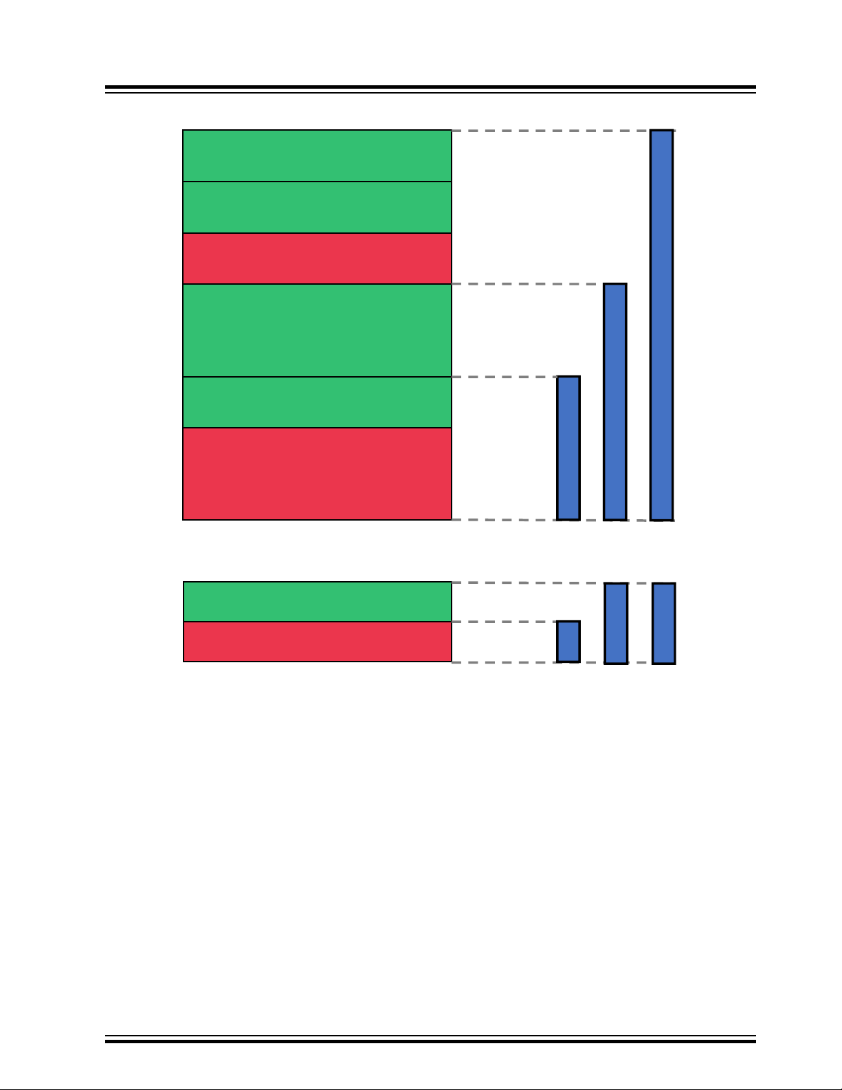
Figure 1-14. ChipErase Commands
CMDCEx:NSSAll
CMDCEx:NSSAll
SecureFlash
(BOOTRegion)
Non‐SecureCallableFlash
(BOOTRegion)
Non‐SecureFlash
(BOOTRegion)
SecureFlash
(APPLICATIONRegion)
Non‐SecureCallableFlash
(APPLICATIONRegion)
Non‐SecureFlash
(APPLICATIONRegion)
SecureDataFlash
Non‐SecureDataFlash
AN5365
Introduction to SAM L11 Security Features
The configuration of the ChipErase command protection Key is done through the BOCOR bit field
configuration, as shown in the following figure.
© 2019 Microchip Technology Inc.
DS70005365B-page 14
Page 15

Introduction to SAM L11 Security Features
Figure 1-15. SAM L11 Configurable ChipErase Key Fuses
AN5365
The different ChipErase commands are used to increase the DAL level without compromising the code
security. Therefore, erase the code before changing to a higher DAL level, as illustrated in the figure
below.
Figure 1-16. SAM L11 DAL and ChipErase Mechanism
The Device Programming Utility provided within Atmel Studio 7 offers the easiest way to set the DAL
commands and ChipErase commands. It can also be used to access device fuses, as shown in the
following figures.
© 2019 Microchip Technology Inc.
DS70005365B-page 15
Page 16

Introduction to SAM L11 Security Features
Figure 1-17. ChipErase Commands Under AS7 Device Programming
AN5365
© 2019 Microchip Technology Inc.
DS70005365B-page 16
Page 17

Introduction to SAM L11 Security Features
Figure 1-18. ChipErase Key Fuses Setting Under AS7 Device Programming
AN5365
1.5 Secure Boot
The SAM L11 Boot ROM is always executed at product startup. This software is ROM coded into the
device and cannot be bypassed by the user. Depending on the Boot Configuration Row (BOCOR) fuse
setting, the Boot ROM knows if a Secure Boot region is defined in the system.
The Boot ROM can perform an integrity check (SHA-256) or authenticate (SHA-256 + BOOTKEY) the
firmware stored in the Secure Boot region prior to executing it. This verification mechanism is a key
element to consider for ensuring the system root of trust during deployment and execution of the Secure
firmware. The following figure illustrates the Secure Boot process with BS (including BNSC) verification.
© 2019 Microchip Technology Inc.
DS70005365B-page 17
Page 18

SecureFlash
(BOOTRegion)
Non‐SecureCallableFlash
(BOOTRegion)
Non‐SecureFlash
(BOOTRegion)
SecureFlash
(APPLICATIONRegion)
Non‐SecureCallableFlash
(APPLICATIONRegion)
Non‐SecureFlash
(APPLICATIONRegion)
0x00000000
BS x0x100– BNSC x0x20
BS x0x100
0x00010000
Flash(Upto64KB)
BootROM
ROM
‐ VerifySecureBoot
Region(optional)
‐ Jumpataddress
0x00000000
Introduction to SAM L11 Security Features
Figure 1-19. Secure Boot Process with BS+BNSC Verification
AN5365
To validate the Secure Bootloader code stored in the Device Flash BS+BNSC memory section, the ROM
code computes the hash of the Flash BS+BNSC regions using the crypto accelerator (CRYA) and
compares it to a reference hash (256 bits/32 bytes) stored in the device BS memory section. This
reference hash (256 bits) must be stored in the last 256 bits of the Secure Flash (BOOT Region) as
shown in the following figure.
© 2019 Microchip Technology Inc.
DS70005365B-page 18
Page 19

AN5365
Introduction to SAM L11 Security Features
Figure 1-20. Boot Secure Reference Hash Location
If the verification result is equal to the reference hashes, the Boot ROM starts the Secure Bootloader
execution. Any mismatch in the value puts the device in an endless reset loop preventing Flash code
execution. Only a ChipErase_ALL command allows the recovery from this device state. The
ChipErase_ALL commands erase the full memory content and reset the fuses to their factory settings.
The following fuses are used in the Secure Boot process configuration:
• BOOTPROT, BS and BSNC: Defines the configuration of the boot section in product Flash. The size
of the Secure, Non-Secure and Non-Secure-Callable boot sections can be customized according to
the application need. These fuses are used for security memory allocation in product IDAU and for
integrity and authentication mechanisms when configured in the BOOTOPT fuse. Any change of the
fuse setting requires a reset to be considered by the device as only the Boot ROM can change IDAU
setting.
• BOOTOPT: Defines the type of verification to be performed as Secure or Non-Secure.
– 0: No verification method
– 1: Integrity check (SHA256)
– 2 or 3: Authentication check (SHA-256 with BOOTKEY)
Note: Using the Secure Boot Authentication feature has an impact on the product start up time. Refer to
the “ SAM L10/L11 Data Sheet” (DS60001513) for additional information.
BOOTKEY: 256-bit BOOTKEY used for Authentication mechanism.
The figure below highlights the fuses used for configuring the Secure boot process.
© 2019 Microchip Technology Inc.
DS70005365B-page 19
Page 20

Figure 1-21. Secure Boot Process Fuses
AN5365
Introduction to SAM L11 Security Features
© 2019 Microchip Technology Inc.
DS70005365B-page 20
Page 21

AN5365
SAM L11 Application Development (Customer A ...
2. SAM L11 Application Development (Customer A and Customer B)
The combination of the system DAL and ChipErase with TrustZone for Cortex-M architecture enables the
developers to follow the following development and deployment approaches:
• Single-developer approach (Customer A)
• Dual-developer approach (Customer A + Customer B)
Atmel Studio 7 integrated development platform provides a full set of advanced features to accelerate the
development of a SAM L11 application. The following sections illustrate the approaches to be followed by
Customer A and Customer B to create and customize their application.
2.1 Single-Developer Approach
In single developer approach, the developer (Customer A) is in charge of developing and deploying
Secure and Non-Secure code. The application of Customer A can be protected by using DAL0. The
figure below illustrates a single developer approach on SAM L11.
Figure 2-1. Single Developer Approach
2.2 Dual-Developer Approach
In this approach, the first developer (Customer A) is in charge of developing the Secure application and
its associated Non-Secure callable library (.lib/.h), and providing a predefined linker file to the second
developer (Customer B). This Secure application is then loaded in the SAM L11 Flash and protected
using the set DAL1 command to prevent further access to the Secure memory region of the device.
A second developer (Customer B) will then start his development on a preprogrammed SAM L11 with
limited access to Secure resources (call to Non-Secure API only). To achieve this, Customer B will use a
linker file and the NSC library provided by customer A. The figure below illustrates a dual developer
approach on SAM L11.
© 2019 Microchip Technology Inc.
DS70005365B-page 21
Page 22

Figure 2-2. Dual-Developer Approach
Blank
SAML11
Securepre‐programmed
L11/Modules
FinalApplication
Non‐secureLinkerfile
+
NSClibrary(.lib/.h)
AN5365
SAM L11 Application Development (Customer A ...
The following sections describe the application development and deployment process to be implemented
for Customer A and Customer B.
2.3 Develop a Secure Solution (Customer A)
To help Customer A to start with SAM L11 (regardless of single or dual developer approaches), Atmel
Studio 7 provides a pre-configured Secure Solution template that illustrates the basic Secure and NonSecure application execution as shown in the figure below. This template can be used to evaluate and
understand the TrustZone for ARMv8-M implementation in the device, or as a start-up point for custom
solution development.
© 2019 Microchip Technology Inc.
DS70005365B-page 22
Page 23

SecureProject
SystemStart
Securefunction1
Securefunction2
NonsecureProject
Userapplication
TrustZone
forCortex‐M
Start
Functioncall
Functioncall
SAM L11 Application Development (Customer A ...
Figure 2-3. Secure Solution Template Overview
AN5365
2.3.1 Creating SAM L11 Secure Solution from Atmel Studio Secure Solution Template
Creating a Secure Solution from the pre-configured template available in Atmel Studio 7 can be done by
following these steps :
1. Open Atmel Studio 7.
2. Select File > New > Project….
3. Configure new solution in the New Project window (See image below):
3.1. Under Installed, select C/C++ .
3.2. Select SAM L11 Secure Solution.
3.3. Enter details for Name, Location, Solution, and Solution Name and then click OK.
© 2019 Microchip Technology Inc.
DS70005365B-page 23
Page 24

SAM L11 Application Development (Customer A ...
Figure 2-4. Creating SAM L11 Solution Under AS7
AN5365
© 2019 Microchip Technology Inc.
DS70005365B-page 24
Page 25

AN5365
SAM L11 Application Development (Customer A ...
When created, the SAM L11 Secure Solution should appear in the Atmel Studio 7 IDE, as shown below:
Figure 2-5. SAM L11 Secure Solution Under AS7
© 2019 Microchip Technology Inc.
DS70005365B-page 25
Page 26

2.3.2 Secure Solution Template Description
BOCOR/UROW files : Contains fuses setting definition
Secure Linker file : Contains link configuration for the
Secure application
Secure Startup file : Contains the Secure vector table and
Secure Reset Handler
Secure System file : Contains the initialization functions
for the system resources allocated to Secure application
Secure .c/.h files : Contains the Secure function examples
Secure Main File : Contains the secure Application main
routine
Veneer .c/.h files : Contains the definition and declaration
of the Non-Secure Callable (NSC) gateway to the secure
functions declared in secure.c/.h
Any solution created from the SAM L11 Secure Solution Template, provided with Atmel Studio 7, is
composed of preconfigured Non-Secure and Secure projects.
All the configuration aspects related to TrustZone for ARMv8-M implementation are already implemented
to facilitate the development process. The following sections describe the content of the template and the
key elements to be modified to customize the solution according to the application needs.
2.3.2.1 Secure Project Description
The goal of the Secure project included in the SAM L11 Secure Solution template is to provide a
preconfigured development base for Secure code development on SAM L11. The Secure project is
preconfigured to illustrate the following applicative aspects of a standard Secure application on SAM L11:
• Device resources attribution to Secure and Non-Secure worlds (fuse settings)
• Initialization of the system security
• Definition and declaration of Secure functions example
• Definition and declaration of Secure gateways with Non-Secure world (veneers)
• Secure call to the Non-Secure application
The following figure describes the file architecture of the preconfigured Secure project:
AN5365
SAM L11 Application Development (Customer A ...
Figure 2-6. Secure Project Architecture
The following figure describes the main routine of the pre-configured Secure project:
© 2019 Microchip Technology Inc.
DS70005365B-page 26
Page 27

Non-Secure Linker file : Contains link configuration for
the Non-Secure application.
Non-Secure Startup file : Contains the Non-Secure
vector table and Non-Secure Reset Handler.
Non-Secure System file : Contains the initialization
functions for the system resources allocated to NonSecure application
Non-Secure Main file : Contains the Non-Secure
Application main routine
Veneer .h file : Link to the veneer header file containing
the secure gateways to secure project
SAM L11 Application Development (Customer A ...
Figure 2-7. Secure Project Main Flowchart
AN5365
This Secure main.c file must be used as a starting point for any secure applications development.
Note: The provided system_init function is empty, therefore system is running 4 MHz (Reset state).
This function should be customized according to the Secure and Non-Secure application requirements.
2.3.2.2 Non-Secure Project Description
The Non-Secure project provided within the SAM L11 Secure Solution Template is a standard application
that runs in a Non-Secure world. This application can use all system resources allocated to the NonSecure world. It uses pre-programmed Non-Secure Callable (NSC) functions using the veneer.h file
provided by the Secure application. The Non-Secure project architecture is shown in the figure below.
Figure 2-8. Non-Secure Project Architecture
The Non-Secure main function flowchart from the Secure Solution Template is shown in the figure below.
© 2019 Microchip Technology Inc.
DS70005365B-page 27
Page 28

SAM L11 Application Development (Customer A ...
Figure 2-9. Non-Secure Project Main Flow Chart
AN5365
The Non-Secure main function illustrates the call of specific Secure functions through gateways provided
by the Secure application veneer.h file.
This Non-Secure main.c file can be used as a starting point for any Non-Secure applications
development.
2.3.2.3 NVM Rows Configuration
To ease the definition and modification of application fuses, the template embeds two dedicated header
files in the SecureApp project for managing the SAM L11 System NVM rows, as shown in the figure
below.
© 2019 Microchip Technology Inc.
DS70005365B-page 28
Page 29

SAM L11 Application Development (Customer A ...
Figure 2-10. saml11_bocor.h and saml11_urow.h
AN5365
These fuses define the configuration of Boot modes, ChipErases, system peripherals (BOD and
watchdog), IDAU (Memory security attribution), and PAC (Peripheral security attribution) and must be
modified according to application needs.
Note: The description of the different NVM rows and bit fields can be found in the “NVM Rows“ chapter
of the “ SAM L10/L11 Data Sheet” (DS60001513).
Any change to the fuse configuration requires a restart of the device, as fuses are handled by the Boot
ROM executed at device start-up. The Boot ROM is responsible for copying the configuration of the fuses
in the different peripheral registers, and then locking the configuration to any users (including Customer
A) until the next boot.
Note: The description of the SAM L11 Boot ROM can be found in the “Boot ROM “ chapter of the “ SAM
L10/L11 Data Sheet” (DS60001513).
The USERROW and BOCOR templates configuration is similar to the device default fuse configuration,
and its associated memory mapping is as shown in the figure below.
© 2019 Microchip Technology Inc.
DS70005365B-page 29
Page 30

SAM L11 Application Development (Customer A ...
Figure 2-11. SAM L11 Secure Template Memory Attribution
AN5365
© 2019 Microchip Technology Inc.
DS70005365B-page 30
Page 31

SAM L11 Application Development (Customer A ...
2.3.2.4 Secure and Non-Secure Projects Linker Files
Secure and Non-Secure projects have their own pre-configured linker files which are available in their
Device_Startup directory. The content of these files is aligned to the memory mapping defined by the
saml11_urow.h and saml11_bocor.h as shown in the figure below.
It is important, in case of Fuse modification to ensure that the memory section definitions are in line with
the new fuse settings and no overlapping is present between the Non-Secure memory space definitions
and the Secure memory space definitions. The figure below illustrates the Secure memory space
definition.
Figure 2-12. Secure Memory Space Definitions
AN5365
The figure below illustrates the Non-Secure memory space definitions
Figure 2-13. Non-Secure Memory Space Definitions
© 2019 Microchip Technology Inc.
DS70005365B-page 31
Page 32

2.3.3 Debugging the Secure Solution
When the device is in DAL = 2, the debugging of the full Solution (Secure + Non-Secure projects) is
allowed. The following steps provide the debug capabilities of the Atmel Studio 7 integrated development
environment for debugging the TrustZone application.
1. Build the solution under Atmel Studio 7.
Note: As the solution is composed of two projects, it is important to re-build and load the full
solution to ensure that the memory content of the device is align with both the project’s source
code.
2. Ensure that the debugger is connected to a computer and SAM L11. Click (Alt+F5) to start
debugging and automatically break on the Secure main function.
Figure 2-14. Debugging and Break on Secure Main Function
AN5365
SAM L11 Application Development (Customer A ...
© 2019 Microchip Technology Inc.
DS70005365B-page 32
Page 33

AN5365
SAM L11 Application Development (Customer A ...
3. Add a breakpoint on the return line of secure_func1 in the Secure project veneer.c file.
Figure 2-15. Breakpoint on secure_func1 Return (Secure Project)
© 2019 Microchip Technology Inc.
DS70005365B-page 33
Page 34

CAUTION
AN5365
SAM L11 Application Development (Customer A ...
4. Add a breakpoint on the return line of func1 in the Secure project Secure_Functions/secure.c
file.
Figure 2-16. Breakpoint on func1 Call (Secure Project)
When debugging the Secure application veneers, only hardware breakpoints must be
used to stop code execution on an SG instruction. Using software breakpoints implies the
addition of a BKP instruction before SG instruction, which triggers a Secure fault during
code execution. This behavior is normal as the first instruction to be executed when
accessing the NSC region must be an SG.
© 2019 Microchip Technology Inc.
DS70005365B-page 34
Page 35

SAM L11 Application Development (Customer A ...
5. Continue debugging by clicking or press <F5>.
As a result, the debugger must stop successively on:
– The Secure function veneer (Secure project)
– The Secure function (Secure project)
Figure 2-17. Break on secure_func1 Return
AN5365
© 2019 Microchip Technology Inc.
DS70005365B-page 35
Page 36

AN5365
SAM L11 Application Development (Customer A ...
Note: A code Disassembly window with step-by-step debug capabilities is available by selecting
the Debug > Windows > disassembly or press <Alt+8>.
Figure 2-18. AS7 Disassembly Window
2.3.4 Protecting the Secure Project Using Debug Access Levels
In a dual developer deployment approach, it is important to protect the Secure memory regions (Secure
Application) from further debugger accesses prior to delivering pre-programmed devices to Customer B
This can be done by changing the debug access level (DAL) to DAL1. Changing the debug access level
can be done using the Device Programing Tool. Follow these steps to change the debug access level:
1. Close the debug session (if running).
2. Open the Device Programming tool by selecting Tools > Device Programming.
3. Send the DAL1 command to the target SAM L11 device as shown in the following figure:
3.1. Select the EDBG Device Programming tool, and then click Apply.
3.2. Under Device Signature, Click Read.
3.3. Select Memories.
3.4. Under Device, Select “Set DAL 1”.
3.5. Click Change DAL.
3.6. Verify that no problem is reported by the Device Programing tool.
© 2019 Microchip Technology Inc.
DS70005365B-page 36
Page 37

3.1
3.2
3.3
3.4
3.5
3.6
SAM L11 Application Development (Customer A ...
Figure 2-19. Changing DAL Using the AS7 Device Programming Tool
AN5365
© 2019 Microchip Technology Inc.
DS70005365B-page 37
Page 38

As a result, setting DAL1 prevents any future debug access to the Secure memory region of the
Notaccessible
Notaccessible
Non‐SecureFlash
(BOOTRegion)
Notaccessible
Notaccessible
Non‐SecureFlash
(APPLICATIONRegion)
0x00000000
BS x0x100– BNSC x0x20
BOOTPROT x0x100
BS x0x100
(BOOTPROT +AS)x0x100–
ANSC x0x20
(BOOTPROT +AS)x0x100
0x00010000
Flash(Upto64KB)
Notaccessible
Non‐SecureSRAM
SRAM(Upto16KB)
Notaccessible
Non‐SecureDataFlash
DataFlash(2KB)
0x400000
0x400000+(RS*0x20)
0x400800
0x20000000
0x20000000+(DS*0x80)
0x20004000
device, as shown in the figure below.
Figure 2-20. DAL Protected Device Memory Region
AN5365
SAM L11 Application Development (Customer A ...
© 2019 Microchip Technology Inc.
DS70005365B-page 38
Page 39

AN5365
SAM L11 Application Development (Customer A ...
Any future debug access to the Secure memory region will be refused by the device and reported
as follows by Atmel Studio 7, as shown in the following figure.
Figure 2-21. Launch Failed error on DAL Protected Area
Important: Further development with the device requires the use of a standalone Non-
Secure project. Refer to the Create and Configure a Non-Secure Project (Customer B).
To reenable debug access on the Secure memory regions, a ChipErase_ALL command
(CE2) must be issued using the device programming tool. The whole device memory and
fuse settings are erased, and the Secure application must be reprogrammed in the
device.
© 2019 Microchip Technology Inc.
DS70005365B-page 39
Page 40

Blank
SAML11
Securepre‐programmed
L11/Modules
FinalApplication
Non‐secureLinkerfile
+
NSClibrary(.lib/.h)
SAM L11 Application Development (Customer A ...
2.4 Develop a Non-Secure Project (Customer B)
In the Customer B context, the development starts with a preprogrammed SAM L11 device that contains
a DAL1 protected Secure project with predefined veneers. See the previous chapter for additional
information.
Figure 2-22. Develop a Non-Secure Project (Customer B)
AN5365
In this context it is mandatory for Customer A to provide Non-Secure resource attribution descriptions,
and Non-Secure callable function API library to Customer B.
Ideally, the approach should be for Customer A to provide a Non-Secure project template to Customer B.
The following sections describe how to create and configure a Non-Secure project for a SAM L11 device
embedding a pre-programmed DAL1 protected Secure application.
2.4.1 Creating a Non-Secure project
Follow these steps to create a Non-Secure project using Atmel Studio 7:
1. Open Atmel Studio 7.
2. Select File > New > Project.
3. Configure the new project in the New Project window:
3.1. From Installed, select C/C++ .
3.2. Select GCC C Executable Project.
3.3. Enter details for Name, Location, and Solution Name.
3.4. Click OK.
© 2019 Microchip Technology Inc.
DS70005365B-page 40
Page 41

AN5365
SAM L11 Application Development (Customer A ...
Figure 2-23. Creating SAM L11 Standalone Non-Secure Project Using Atmel Studio 7
4. Select the ATSAML11E16A device in the Device Selection window, and then click OK.
Figure 2-24. SAM L11 Product Selection for New SAM L11 Standalone Non-Secure Project
The Non-Secure project appears in Atmel Studio 7 IDE, as shown in the following figure.
© 2019 Microchip Technology Inc.
DS70005365B-page 41
Page 42

SAM L11 Application Development (Customer A ...
Figure 2-25. Standalone SAM L11 Non-Secure Project
AN5365
2.4.2 Project Configuration
After creating a Non-Secure project, follow these steps to configure it according to the pre-programed
Secure project mapping and Secure gateway APIs:
• Configure the project by aligning its linker file to the Secure and Non-Secure memories attribution
predefined by Customer A.
• Link the Secure gateway library to the project and add veneer header file to the project.
© 2019 Microchip Technology Inc.
DS70005365B-page 42
Page 43

SecureFlash
(APPLICATIONRegion)
Non‐SecureCallableFlash
(APPLICATIONRegion)
Non‐SecureFlash
(APPLICATIONRegion)
0x00000000
0x00007C00
0x00010000
Flash(Upto64KB)
SecureSRAM
Non‐SecureSRAM
SRAM(Upto16KB)
0x20000000
0x20002000
0x20004000
0x00008000
SAM L11 Application Development (Customer A ...
2.4.2.1 Align Project Linker File to the SAM L11 Non-Secure Memories Attribution
Follow these steps to modify the Non-Secure solution project linker file according to the Secure and NonSecure memory space allocation as illustrated in the following figure.
Figure 2-26. Secure and Non-Secure Memory Space
AN5365
© 2019 Microchip Technology Inc.
DS70005365B-page 43
Page 44

SAM L11 Application Development (Customer A ...
1. Open the project linker file: Device Startup/saml11e16a_flash.ld.
Figure 2-27. Non-Secure Project Linker File Location
AN5365
2. Update the linker file memory space definitions according to the SAM L11 Non-Secure memory
attribution.
/* Memory Spaces Definitions */
MEMORY
{
rom (rx) : ORIGIN = 0x00008000, LENGTH = 0x00008000
ram (rwx) : ORIGIN = 0x20002000, LENGTH = 0x00002000
}
© 2019 Microchip Technology Inc.
DS70005365B-page 44
Page 45

SAM L11 Application Development (Customer A ...
Figure 2-28. Non-Secure Memory Address and Size Definition
AN5365
2.4.2.2 Adding and Linking Secure Gateway Library to Non-Secure Project
Follow these steps to add and link the Secure gateway library that is generated during Secure application
development provided by Customer A:
1. Copy the Secure project implib to the Non-Secure project.
Figure 2-29. Adding Secure Gateway Library File to Non-Secure Project Sources
© 2019 Microchip Technology Inc.
DS70005365B-page 45
Page 46

SAM L11 Application Development (Customer A ...
2. In Atmel Studio 7, right click on the Non-Secure project, and then select Properties.
Figure 2-30. Accessing to Non-Secure Project Properties
AN5365
© 2019 Microchip Technology Inc.
DS70005365B-page 46
Page 47

AN5365
SAM L11 Application Development (Customer A ...
3. To add the Secure Project library, from Toolchain > ARM/GNU Linker > Libraries, and then click
Add Item.
Figure 2-31. Add New Library to the Link Option
4. Under Libraries section, enter library name.
Figure 2-32. Adding Secure Gateway Library Name
© 2019 Microchip Technology Inc.
DS70005365B-page 47
Page 48

SAM L11 Application Development (Customer A ...
5. Add the Secure Project library path, from Toolchain > ARM/GNU Linker > Libraries.
6. Click Add Item.
Figure 2-33. Add New Library Search Path
AN5365
7. Under Library search path, browse and select the location of the Secure project implib.
8. Select Relative Path to ensure project portability, and then click OK.
Figure 2-34. Enter Relative Path to the Secure Gateway Library
© 2019 Microchip Technology Inc.
DS70005365B-page 48
Page 49

SAM L11 Application Development (Customer A ...
9. The Linker Library properties must be displayed as shown in the following figure:
Figure 2-35. Non-Secure Project Linker Libraries Configuration
AN5365
10. Click (Save button) to save the project settings.
2.4.2.3 Adding and Including Secure Gateway Header File
To add and include a secure gateway header file, perform these actions:
1. Copy the Secure gateway header file from the Secure project to the Non-Secure project.
Figure 2-36. Including Secure Gateway Header File in Non-Secure Project Sources
2. Right click Non-Secure project in the solution explorer, and then select Add > Existing Item.
© 2019 Microchip Technology Inc.
DS70005365B-page 49
Page 50

SAM L11 Application Development (Customer A ...
Figure 2-37. Including Secure Gateway Header File in AS7 Solution Explorer
AN5365
3. Select the Secure gateway header file, and then click Add.
© 2019 Microchip Technology Inc.
DS70005365B-page 50
Page 51

SAM L11 Application Development (Customer A ...
Figure 2-38. Including Secure Gateway Header File in Non-Secure Project
4. Right click Non-Secure project in the Solution explorer, and then select Properties.
Figure 2-39. Accessing Non-Secure Project Properties Under AS7
AN5365
© 2019 Microchip Technology Inc.
DS70005365B-page 51
Page 52

AN5365
SAM L11 Application Development (Customer A ...
5. In the Non-Secure project property window, select Toolchain > ARM/GNU C Compiler > Directories,
and then click Add Item.
Figure 2-40. Adding New Compiler Directory to Non-secure Project
6. Under Include Paths, select the location of the veneer.h file.
7. Select Relative Path to ensure project portability, and then click OK.
Figure 2-41. Including Secure Gateway Library Path in Compiler Directory
8. The Compiler Directories properties will be displayed.
© 2019 Microchip Technology Inc.
DS70005365B-page 52
Page 53

SAM L11 Application Development (Customer A ...
Figure 2-42. Non-Secure Project Compiler Directories Parameters
AN5365
9. Press (Save button) to save the project settings.
© 2019 Microchip Technology Inc.
DS70005365B-page 53
Page 54

AN5365
SAM L11 Application Development (Customer A ...
10. To add the Secure gateway library, add the highlighted code at the beginning of the main.c file.
Figure 2-43. Including veneer.h in Non-Secure Project main.c File
11. Click (Save button) to save the modification to the main.c file.
12. Click (Build Project button).
13. Verify that no error is reported by the build process.
14. Launch debug session and confirm it is working.
Important: Prior to loading the project on the target SAM L11 device, it is important to
check Project Properties> Tools> Programing settings and ensure that the programming
process does not execute a ChipErase_All command prior to loading the application.
The Ideal configuration is “Erase only Program area” as shown in the following figure.
© 2019 Microchip Technology Inc.
DS70005365B-page 54
Page 55

SAM L11 Application Development (Customer A ...
Figure 2-44. Project Program Settings
AN5365
Figure 2-45. Non-Secure Project Successful Build
15. Launch the debug session and verify whether the project is working or not.
Important: Debugging the Non-Secure project requires a compatible preprogrammed
Secure application that configures and starts the Non-Secure execution. If this Secure
application is not available on the chip, the debug process will hang.
© 2019 Microchip Technology Inc.
DS70005365B-page 55
Page 56

SecureFlash(BOOTRegion)
Non‐SecureCallableFlash(BOOTRegion)
Non‐SecureFlash(BOOTRegion)
SecureFlash
(APPLICATIONRegion)
Non‐SecureCallableFlash
(APPLICATIONRegion)
Non‐SecureFlash
(APPLICATIONRegion)
0x00000000
BS x0x100– BNSC x0x20
BOOTPROT x0x100
BS x0x100
(BOOTPROT +AS)x
0x100– ANSC x0x20
(BOOTPROT +AS)x0x100
0x00010000
Flash(Upto64KB)
Chiperase_NS
Chiperase_S
Chiperase_All
ChipErase
Flash(Upto64KB)
SAM L11 Application Development (Customer A ...
2.5 Developing Solution with Secure Boot Program (Customer A)
The SAM L11 device offers two configurable memory sections for storing the Secure and Non-Secure
boot programs. These two sections are protected against ChipErase_S and ChipErase_NS offering
possibilities to store Secure and Non-Secure Bootloader code as shown in the following figure.
Figure 2-46. Application with Secure and Non-Secure Boot Programs
AN5365
In addition to ChipErase protection, the product Boot ROM offers the possibility to perform an integrity
check or authenticate the firmware stored in the Secure Boot section prior to executing it. This verification
mechanism is a key element to consider for ensuring the system root of trust during deployment and
2.5.1 Creating a Secure Solution with Boot Program
execution of the Secure firmware.
To ease the development of an application with the Secure Boot program, Atmel Studio 7 provides a
predefined Secure Solution with a Boot template. This template can be used to evaluate and understand
the solution architecture and start the development of a custom application featuring a Secure Boot
project. The following figure shows the template content and interactions between preconfigured projects.
© 2019 Microchip Technology Inc.
DS70005365B-page 56
Page 57

SecureProject
SystemStart
Securefunction1
Securefunction2
NonsecureProject
Userapplication
TrustZonefor
Cortex
‐
M
Functioncall
Functioncall
SecureBootProject
SystemStart
Securebootfunction
1
Securebootfunction
2
Functioncall
Functioncall
Start
Start
SAM L11 Application Development (Customer A ...
Figure 2-47. Secure Solution Template Content
AN5365
Follow these steps to create a Secure solution with a Boot program using Atmel Studio 7.
1. Open Atmel Studio 7.
2. From File > New > Project….
3. Select “C/C++”.
4. Select “SAM L11 Secure Solution with Boot”.
5. Enter details for Name, Location, and Solution Name.
6. Click OK.
© 2019 Microchip Technology Inc.
DS70005365B-page 57
Page 58

3
4
5
6
SAM L11 Application Development (Customer A ...
Figure 2-48. Secure Solution with Boot Creation
AN5365
© 2019 Microchip Technology Inc.
DS70005365B-page 58
Page 59

SAM L11 Application Development (Customer A ...
When created, the solution appears in Atmel Studio 7 IDE as shown in the following figure:
Figure 2-49. Secure Solution with Boot
AN5365
© 2019 Microchip Technology Inc.
DS70005365B-page 59
Page 60

Secure Linker file : Contains link configuration for the
Secure boot application
Secure Startup file : Contains the Secure boot vector
table and Secure Reset Handler
Secure System file : Contains the initialization functions
for the system resources allocated to Secure application
Secure .c/.h files : Contains the Secure function examples
Secure Main File : Contains the secure Application main
routine
Veneer .c/.h files : Contains the definition and declaration
of the Non-Secure Callable (NSC) gateway to the secure
functions declared in secure.c/.h
BOCOR/UROW files : Contains fuses setting definition
SAM L11 Application Development (Customer A ...
2.5.2 Secure Solution Template with Boot Description
The SAM L11 Secure solution template with boot code provided within Atmel Studio 7 is similar to the
SAM L11 Secure solution template as described in previous chapters, but it embeds a Secure Boot
program (stored in BS+BNSC memory region of the device).
2.5.2.1 Template Secure Boot Project Description
The goal of the Secure Boot project included in the solution template is to provide a preconfigured
development base for Secure boot code development on SAM L11 . The Secure project is preconfigured
to illustrate the following aspects of a standard Secure application on the SAM L11:
• Definition and declaration of Secure boot functions example
• Definition and declaration of Secure boot gateways with Non-Secure world (veeners)
• Secure call to the Secure application
The following figure illustrates the file architecture of the pre-configured Secure Project:
Figure 2-50. Secure Boot Project Architecture
AN5365
© 2019 Microchip Technology Inc.
DS70005365B-page 60
Page 61

2.5.2.2 Template NVM Fuses Configuration
SecureFlash
(BOOTRegion)
Non‐SecureCallableFlash
(BOOTRegion)
SecureFlash
(APPLICATIONRegion)
Non‐SecureCallableFlash
(APPLICATIONRegion)
Non‐SecureFlash
(APPLICATIONRegion)
0x00000000
0x00000A00
0x00001A00
0x00001000
0x0000D000
0x00010000
Flash(Upto64KB)
SecureSRAM
Non‐SecureSRAM
SRAM(Upto16KB)
SecureDataFlash
DataFlash(2KB)
0x20000000
0x20002000
0x20004000
0x00400000
0x00400400
0x00400800
The default USERROW and BOCOR template settings and associated memory mapping are described in
the following figure.
Figure 2-51. Default Secure Solution with Boot Code Mapping
AN5365
SAM L11 Application Development (Customer A ...
The table below provides the BOCOR Fuse settings.
Table 2-1. BOCOR Fuse Settings
Fuses values Configuration
BNSC 0x30 Boot Flash Non-Secure Callable Size = BNSC*0x20 = 0x600
BS 0x10 Boot Flash Secure Size = BS*0x100 = 0x1000
BOOTOPT 0x00 No secure boot verification
© 2019 Microchip Technology Inc.
DS70005365B-page 61
Page 62

SAM L11 Application Development (Customer A ...
...........continued
Fuses values Configuration
BOOTPROT 0x10 Boot Protection size = BOOTPROT*0x100 = 0x1000
BCWEN 0x01 Boot Configuration Write Enabled
BCREN 0x01 Boot Configuration Read Enabled
CEKEY0 All 1s CE0 key = All 1s
CEKEY1 All 1s CE1 key = All 1s
CEKEY2 All 1s CE2 key = All 1s
BOOTKEY All 1s Boot key = All 1s
The table below provides the UROW Fuse settings.
Table 2-2. UROW Fuse Settings
Fuses values Configuration
SULCK_BS 0x1 BS region is not locked
AN5365
SULCK_AS 0x1 AS region is not locked
SULCK_DS 0x1 DS region is not locked
NSULCK_BNS 0x1 BNS region is not locked
NSULCK_ANS 0x1 ANS region is not locked
NSULCK_DNS 0x1 DNS region is not locked
BOD33_LEVEL 0x6 BOD33 threshold level = 0x6
BOD33_DISABLE 0x0 BOD33 enabled
BOD33_ACTION 0x1 BOD Action = RESET
WDT_RUNSTDBY 0x0 WDT disabled during standby sleep
WDT_ENABLE 0x0 WDT disabled
WDT_ALWAYS_ON 0x0 WDT enabled/disabled through ENABLE bit
WDT_PER 0xB WDT Time-Out Period = 0xB
WDT_WINDOW 0xB Window Mode Time-Out Period = 0xB
WDT_EWOFFSET 0xB Early Warning Interrupt Time Offset = 0xB
WDT_WEN 0x0 WDT windows disabled
BOD33_HYST 0x0 No BOD33 Hysteresis
RXN 0x1 RAM is not executable
DXN 0x1 Data Flash is not executable
AS 0x10 Flash Application Secure Size = AS*0x100 = 0x1000
ANSC 0x30 Flash Application Non-Secure Callable Size = ANSC*0x20 = 0x600
© 2019 Microchip Technology Inc.
DS70005365B-page 62
Page 63

AN5365
SAM L11 Application Development (Customer A ...
...........continued
Fuses values Configuration
DS 0x08 Data Flash Secure Size = DS*0x100 = 0x800
RS 0x40 RAM Secure Size = RS*0x80 = 0x2000
URWEN 0x1 User Row Write Enabled
NONSECA 0x0000 0000 Peripherals are secured
NONSECB 0x0000 0000 Peripherals are secured
NONSECC 0x0000 0000 Peripherals are secured
To ease the definition and modification of application fuses, all fuse values are defined in
saml11_bocor.h and saml11_urow.h as shown in the following figure. These fuse values can be
modified according to the requirement of the application.
Figure 2-52. SAM L11 Fuses Definition
© 2019 Microchip Technology Inc.
DS70005365B-page 63
Page 64

SAM L11 Application Development (Customer A ...
2.5.2.3 Enabling Secure Boot Process with BS+BNSC Verification
Follow these steps to enable Secure Boot process verification when working with Atmel Studio 7:
1. Perform a ChipErase_ALL command using device programming.
2. Build the Boot application using Atmel Studio IDE.
3. Change BOOTOPT fuse to 0x01 or 0x02 using the device programing tool.
Figure 2-53. Secure Boot Process with BS+BNSC Verification
AN5365
© 2019 Microchip Technology Inc.
DS70005365B-page 64
Page 65

Ref.Hash
BNSC
AN5365
SAM L11 Application Development (Customer A ...
The reference hash will be computed and written in memory automatically by the device programming
tool when the step, shown in the figure below, is executed.
Figure 2-54. Secure Boot Application Reference Hash
© 2019 Microchip Technology Inc.
DS70005365B-page 65
Page 66

3. Software Use Case Examples
3.1 Non-Secure Peripheral (TC0)
This Use Case example describes how to configure a SAM L11 integrated peripheral (TC0) as a NonSecure peripheral.
In this example, the Secure project is in charge of allocating PORT and TC peripherals to the Non-Secure
world, setting system clocks, and then jumping to the Non-Secure application.
The Non-Secure application uses the TC0 to generate a PWM signal on PA07.
The figure below illustrate the execution flow of Secure main routines.
Figure 3-1. Secure Main Routine Flow Chart
AN5365
Software Use Case Examples
The figure below illustrate the execution flow of Non-Secure main routines.
© 2019 Microchip Technology Inc.
DS70005365B-page 66
Page 67

Figure 3-2. Non-Secure Main Routine Flow Chart
AN5365
Software Use Case Examples
The following code examples provide the key Secure world function calls and declaration used for
allocating TC0 and associated system features to the Non-Secure world.
• TC0 allocation to the Non-Secure world in fuses definition (saml11_urow.h)
…
#define UROW_NONSECC_SERCOM0 0x0 /* SERCOM0 is secured */
#define UROW_NONSECC_SERCOM1 0x0 /* SERCOM1 is secured */
#define UROW_NONSECC_SERCOM2 0x0 /* SERCOM2 is secured */
#define UROW_NONSECC_TC0 0x1 /* TC0 is Non-secured */
#define UROW_NONSECC_TC1 0x0 /* TC1 is secured */
#define UROW_NONSECC_TC2 0x0 /* TC2 is secured */
…
• TC0 peripheral clock configuration and interrupt allocation to the Non-Secure world (Secure
application)
int main(void)
{
uint32_t ret;
funcptr_void NonSecure_ResetHandler;
/* Initialize the SAM system */
SystemInit();
/* Configure TC0 peripheral clock channel */
GCLK->PCHCTRL[14].reg =(GCLK_PCHCTRL_GEN(0) | GCLK_PCHCTRL_CHEN);
© 2019 Microchip Technology Inc.
DS70005365B-page 67
Page 68

/* Allocate PA07 (LED pin) to Non Secure world */
PORT_SEC->Group[0].NONSEC.reg = (PORT_PA07);
/* Allocate TC0 interrupt to Non-Secure world */
NVIC_SetTargetState(TC0_IRQn);
/* Set Non-Secure main stack (MSP_NS) */
TZ_set_MSP_NS(*((uint32_t *)(TZ_START_NS)));
/* Get Non-Secure reset handler */
NonSecure_ResetHandler = (funcptr_void)(*((uint32_t *)((TZ_START_NS) + 4U)));
/* Start Non-Secure state software application */
NonSecure_ResetHandler();
while (1)
{
NOP();
}
}
3.2 Secure Peripheral (TC0)
This use case example demonstrates how to configure a SAM L11 integrated peripheral (TC0) as a
Secure peripheral.
In this use case, the Secure project is in charge of configuring system resources and managing the TC
peripheral. It also provides specific TC0 APIs and Non-Secure callbacks to the Non-Secure world. The
figure below illustrates the secure main function:
AN5365
Software Use Case Examples
Figure 3-3. Secure Main Routine Flow Chart
© 2019 Microchip Technology Inc.
DS70005365B-page 68
Page 69

AN5365
Software Use Case Examples
The following APIs or veneers are provided to Non-Secure world to drive TC0 peripheral from NonSecure world:
• tc0_compare_0_interrupt_callback_register(secure_void_cb_t pfunction);
• tc0_overflow_interrupt_callback_register(secure_void_cb_t pfunction);
• tc0_init(void);
• tc0_set_duty_cycle(uint8_t duty_cycle);
The Non-Secure world use the Secured TC0 through APIs and veneers provided by the Secure world
and generates a PWM signal on the PA07 pin. The following figures display the flowcharts of the
application and the interaction with the Secure world.
Figure 3-4. Non-Secure Main Routine Flow Chart
The figure below illustrates the Secure TC handler.
© 2019 Microchip Technology Inc.
DS70005365B-page 69
Page 70

Figure 3-5. Secure TC Handler Flow Chart
AN5365
Software Use Case Examples
3.3 Mix-Secure Peripheral (EIC)
This use case example describes how to configure and use a SAM L11 Mix-Secure peripheral (EIC).
Using this example, the user can configure two interrupt lines, EXTIN 1 and EXTIN2, and then allocate
them to the Non-Secure and Secure world. This results in the execution of a Non-Secure handler when
EXTIN 1 interrupt is detected and a Secure Handler when the EXTIN 2 is detected, as shown in the figure
below.
© 2019 Microchip Technology Inc.
DS70005365B-page 70
Page 71

Figure 3-6. Mix-Secure Peripheral Use Case Example Output
AN5365
Software Use Case Examples
In the example, the Secure project is in charge of configuring system resources, allocating EIC interrupt
line 1 to the Non-Secure world, and managing the external interrupt on Secured interrupt line 2. The
figure below illustrates the Secure main function flowchart.
© 2019 Microchip Technology Inc.
DS70005365B-page 71
Page 72

Figure 3-7. Secure Application Flow Chart
AN5365
Software Use Case Examples
In the example, the Non-Secure project is in charge of configuring and handling the EIC interrupt line 1,
which is allocated to the Non-Secure world by the Secure application. The figure below illustrates this
process:
© 2019 Microchip Technology Inc.
DS70005365B-page 72
Page 73

Figure 3-8. Non-Secure Application Flow Chart
AN5365
Software Use Case Examples
© 2019 Microchip Technology Inc.
DS70005365B-page 73
Page 74

3.4 TrustRAM
The TrustRAM (TRAM) embedded in the SAM L11 offers these advanced security features for Secure
information storage:
• Address and data scrambling
• Silent access
• Data remanence
• Active shielding and tamper detection
• Full erasure of scramble key and RAM data on tamper detection
The TrustRAM example, provided with this document, illustrates the configuration of TrustRAM with the
following security features:
• Address and data scrambling activated with key: 0xCAFE
• Silent access enabled
• Data remanence enabled
• RTC static tamper detection enabled on PA8
• Full erasure of scramble key and RAM data on tamper detection enabled
AN5365
Software Use Case Examples
In this example, the TrustRAM content is displayed and refreshed every second on a Secure console
(USART0), allowing users to experiment with static and dynamic tamper detections coupled with a
TrustRAM Full Erase.
Figure 3-9. TRAM Use Case Application Output
The figure below illustrates the Secure main function with TRAM.
© 2019 Microchip Technology Inc.
DS70005365B-page 74
Page 75

Figure 3-10. TRAM Use Case Application Flow Chart
AN5365
Software Use Case Examples
© 2019 Microchip Technology Inc.
DS70005365B-page 75
Page 76

3.5 Cryptographic Accelerator (CRYA)
SAM L11 embeds a hardware Cryptographic Accelerator (CRYA) with associated software functions
stored in Boot ROM, which provide the hardware acceleration for the following:
• Advanced Encryption Standard (AES-128) encryption and decryption
• Secure Hash Algorithm 2 (SHA-256) authentication
• Galois Counter Mode (GCM) encryption and authentication
The below CRYA example shows the use of CRYA for AES 128-bit key length and the SHA-256
cryptographic algorithm.
Figure 3-11. CRYA Use Case Application Output
AN5365
Software Use Case Examples
The figure below illustrates the CRYA use case application flowchart:
© 2019 Microchip Technology Inc.
DS70005365B-page 76
Page 77

Figure 3-12. CRYA Use Case Application Flow Chart
AN5365
Software Use Case Examples
© 2019 Microchip Technology Inc.
DS70005365B-page 77
Page 78

3.6 Data Flash
The Data Flash embedded in SAM L11 offers the following advanced security features for the secure
information storage:
• Data scrambling
• Silent access to selected row (TEROW)
• Tamper erase of selected row (TEROW) on tamper detection
The Data Flash use case shown in the figure below, illustrates the configuration of NVMCTRL for Secure
Data Flash management:
• Data scrambling activated with key: 0x1234
• Silent access enabled on the first Data Flash ROW
Figure 3-13. Data Flash Use Case Application Output
AN5365
Software Use Case Examples
© 2019 Microchip Technology Inc.
DS70005365B-page 78
Page 79

The figure below illustrates Data Flash use case application flowchart:
Figure 3-14. Data Flash Use Case Application Flow Chart
AN5365
Software Use Case Examples
© 2019 Microchip Technology Inc.
DS70005365B-page 79
Page 80

4. Revision History
Revision A - June 2018
Initial release of this document.
Revision B - April 2019
Document restructuring:
• A new section is added for developing a Secure application: Develop a Solution with a Secure Boot
Program (Customer A)
• The topic Application Deployment with Secure and Non-Secure Bootloaders was removed and the
content incorporated into Introduction to SAM L11 Security Features
• The topic How to Define and Use Secure and Non-Secure Peripherals was removed and the content
incorporated into Software Use Case Examples
• Introduction was rewritten to reflect updates to the document.
The following sections were updated:
• TrustZone for ARMv8-M updated with new images
• Secure and Non-Secure Peripheralsupdated with new images
• Mix-Secure Integrated Peripheralsupdated with new images
• Debug Access Level (DAL) and Chip Eraseupdated with new diagrams
• Secure Bootupdated with new images
• Single Developer Approachupdated with new images
• Dual Developer Approachupdated with new images
• Develop a Secure Solution (Customer A)updated with new images
• Develop a Non-Secure Project (Customer B)updated with new images
• Non-Secure Peripheralsupdated with new diagrams and code blocks
• Secure Peripheralsupdated with new diagrams
• Mix-Secure Peripheralsupdated with new diagrams
• TrustRAM (TRAM)updated with new images
• Cryptographic Accelerator (CRYA)updated with new images
• DATA Flashupdated with new images
AN5365
Revision History
© 2019 Microchip Technology Inc.
DS70005365B-page 80
Page 81

AN5365
The Microchip Web Site
Microchip provides online support via our web site at http://www.microchip.com/. This web site is used as
a means to make files and information easily available to customers. Accessible by using your favorite
Internet browser, the web site contains the following information:
• Product Support – Data sheets and errata, application notes and sample programs, design
resources, user’s guides and hardware support documents, latest software releases and archived
software
• General Technical Support – Frequently Asked Questions (FAQ), technical support requests, online
discussion groups, Microchip consultant program member listing
• Business of Microchip – Product selector and ordering guides, latest Microchip press releases,
listing of seminars and events, listings of Microchip sales offices, distributors and factory
representatives
Customer Change Notification Service
Microchip’s customer notification service helps keep customers current on Microchip products.
Subscribers will receive e-mail notification whenever there are changes, updates, revisions or errata
related to a specified product family or development tool of interest.
To register, access the Microchip web site at http://www.microchip.com/. Under “Support”, click on
“Customer Change Notification” and follow the registration instructions.
Customer Support
Users of Microchip products can receive assistance through several channels:
• Distributor or Representative
• Local Sales Office
• Field Application Engineer (FAE)
• Technical Support
Customers should contact their distributor, representative or Field Application Engineer (FAE) for support.
Local sales offices are also available to help customers. A listing of sales offices and locations is included
in the back of this document.
Technical support is available through the web site at: http://www.microchip.com/support
Microchip Devices Code Protection Feature
Note the following details of the code protection feature on Microchip devices:
• Microchip products meet the specification contained in their particular Microchip Data Sheet.
• Microchip believes that its family of products is one of the most secure families of its kind on the
market today, when used in the intended manner and under normal conditions.
• There are dishonest and possibly illegal methods used to breach the code protection feature. All of
these methods, to our knowledge, require using the Microchip products in a manner outside the
operating specifications contained in Microchip’s Data Sheets. Most likely, the person doing so is
engaged in theft of intellectual property.
• Microchip is willing to work with the customer who is concerned about the integrity of their code.
© 2019 Microchip Technology Inc.
DS70005365B-page 81
Page 82

AN5365
• Neither Microchip nor any other semiconductor manufacturer can guarantee the security of their
code. Code protection does not mean that we are guaranteeing the product as “unbreakable.”
Code protection is constantly evolving. We at Microchip are committed to continuously improving the
code protection features of our products. Attempts to break Microchip’s code protection feature may be a
violation of the Digital Millennium Copyright Act. If such acts allow unauthorized access to your software
or other copyrighted work, you may have a right to sue for relief under that Act.
Legal Notice
Information contained in this publication regarding device applications and the like is provided only for
your convenience and may be superseded by updates. It is your responsibility to ensure that your
application meets with your specifications. MICROCHIP MAKES NO REPRESENTATIONS OR
WARRANTIES OF ANY KIND WHETHER EXPRESS OR IMPLIED, WRITTEN OR ORAL, STATUTORY
OR OTHERWISE, RELATED TO THE INFORMATION, INCLUDING BUT NOT LIMITED TO ITS
CONDITION, QUALITY, PERFORMANCE, MERCHANTABILITY OR FITNESS FOR PURPOSE.
Microchip disclaims all liability arising from this information and its use. Use of Microchip devices in life
support and/or safety applications is entirely at the buyer’s risk, and the buyer agrees to defend,
indemnify and hold harmless Microchip from any and all damages, claims, suits, or expenses resulting
from such use. No licenses are conveyed, implicitly or otherwise, under any Microchip intellectual
property rights unless otherwise stated.
Trademarks
The Microchip name and logo, the Microchip logo, AnyRate, AVR, AVR logo, AVR Freaks, BeaconThings,
BitCloud, CryptoMemory, CryptoRF, dsPIC, FlashFlex, flexPWR, Heldo, JukeBlox, KeeLoq, KeeLoq logo,
Kleer, LANCheck, LINK MD, maXStylus, maXTouch, MediaLB, megaAVR, MOST, MOST logo, MPLAB,
OptoLyzer, PIC, picoPower, PICSTART, PIC32 logo, Prochip Designer, QTouch, RightTouch, SAM-BA,
SpyNIC, SST, SST Logo, SuperFlash, tinyAVR, UNI/O, and XMEGA are registered trademarks of
Microchip Technology Incorporated in the U.S.A. and other countries.
ClockWorks, The Embedded Control Solutions Company, EtherSynch, Hyper Speed Control, HyperLight
Load, IntelliMOS, mTouch, Precision Edge, and Quiet-Wire are registered trademarks of Microchip
Technology Incorporated in the U.S.A.
Adjacent Key Suppression, AKS, Analog-for-the-Digital Age, Any Capacitor, AnyIn, AnyOut, BodyCom,
chipKIT, chipKIT logo, CodeGuard, CryptoAuthentication, CryptoCompanion, CryptoController,
dsPICDEM, dsPICDEM.net, Dynamic Average Matching, DAM, ECAN, EtherGREEN, In-Circuit Serial
Programming, ICSP, Inter-Chip Connectivity, JitterBlocker, KleerNet, KleerNet logo, Mindi, MiWi,
motorBench, MPASM, MPF, MPLAB Certified logo, MPLIB, MPLINK, MultiTRAK, NetDetach, Omniscient
Code Generation, PICDEM, PICDEM.net, PICkit, PICtail, PureSilicon, QMatrix, RightTouch logo, REAL
ICE, Ripple Blocker, SAM-ICE, Serial Quad I/O, SMART-I.S., SQI, SuperSwitcher, SuperSwitcher II, Total
Endurance, TSHARC, USBCheck, VariSense, ViewSpan, WiperLock, Wireless DNA, and ZENA are
trademarks of Microchip Technology Incorporated in the U.S.A. and other countries.
SQTP is a service mark of Microchip Technology Incorporated in the U.S.A.
Silicon Storage Technology is a registered trademark of Microchip Technology Inc. in other countries.
GestIC is a registered trademark of Microchip Technology Germany II GmbH & Co. KG, a subsidiary of
Microchip Technology Inc., in other countries.
All other trademarks mentioned herein are property of their respective companies.
© 2019 Microchip Technology Inc.
DS70005365B-page 82
Page 83

AN5365
©
2018, Microchip Technology Incorporated, Printed in the U.S.A., All Rights Reserved.
ISBN: 978-1-5224-4347-6
Quality Management System Certified by DNV
ISO/TS 16949
Microchip received ISO/TS-16949:2009 certification for its worldwide headquarters, design and wafer
fabrication facilities in Chandler and Tempe, Arizona; Gresham, Oregon and design centers in California
and India. The Company’s quality system processes and procedures are for its PIC® MCUs and dsPIC
DSCs, KEELOQ® code hopping devices, Serial EEPROMs, microperipherals, nonvolatile memory and
analog products. In addition, Microchip’s quality system for the design and manufacture of development
systems is ISO 9001:2000 certified.
®
© 2019 Microchip Technology Inc.
DS70005365B-page 83
Page 84

Worldwide Sales and Service
AMERICAS ASIA/PACIFIC ASIA/PACIFIC EUROPE
Corporate Office
2355 West Chandler Blvd.
Chandler, AZ 85224-6199
Tel: 480-792-7200
Fax: 480-792-7277
Technical Support:
http://www.microchip.com/
support
Web Address:
www.microchip.com
Atlanta
Duluth, GA
Tel: 678-957-9614
Fax: 678-957-1455
Austin, TX
Tel: 512-257-3370
Boston
Westborough, MA
Tel: 774-760-0087
Fax: 774-760-0088
Chicago
Itasca, IL
Tel: 630-285-0071
Fax: 630-285-0075
Dallas
Addison, TX
Tel: 972-818-7423
Fax: 972-818-2924
Detroit
Novi, MI
Tel: 248-848-4000
Houston, TX
Tel: 281-894-5983
Indianapolis
Noblesville, IN
Tel: 317-773-8323
Fax: 317-773-5453
Tel: 317-536-2380
Los Angeles
Mission Viejo, CA
Tel: 949-462-9523
Fax: 949-462-9608
Tel: 951-273-7800
Raleigh, NC
Tel: 919-844-7510
New York, NY
Tel: 631-435-6000
San Jose, CA
Tel: 408-735-9110
Tel: 408-436-4270
Canada - Toronto
Tel: 905-695-1980
Fax: 905-695-2078
Australia - Sydney
Tel: 61-2-9868-6733
China - Beijing
Tel: 86-10-8569-7000
China - Chengdu
Tel: 86-28-8665-5511
China - Chongqing
Tel: 86-23-8980-9588
China - Dongguan
Tel: 86-769-8702-9880
China - Guangzhou
Tel: 86-20-8755-8029
China - Hangzhou
Tel: 86-571-8792-8115
China - Hong Kong SAR
Tel: 852-2943-5100
China - Nanjing
Tel: 86-25-8473-2460
China - Qingdao
Tel: 86-532-8502-7355
China - Shanghai
Tel: 86-21-3326-8000
China - Shenyang
Tel: 86-24-2334-2829
China - Shenzhen
Tel: 86-755-8864-2200
China - Suzhou
Tel: 86-186-6233-1526
China - Wuhan
Tel: 86-27-5980-5300
China - Xian
Tel: 86-29-8833-7252
China - Xiamen
Tel: 86-592-2388138
China - Zhuhai
Tel: 86-756-3210040
India - Bangalore
Tel: 91-80-3090-4444
India - New Delhi
Tel: 91-11-4160-8631
India - Pune
Tel: 91-20-4121-0141
Japan - Osaka
Tel: 81-6-6152-7160
Japan - Tokyo
Tel: 81-3-6880- 3770
Korea - Daegu
Tel: 82-53-744-4301
Korea - Seoul
Tel: 82-2-554-7200
Malaysia - Kuala Lumpur
Tel: 60-3-7651-7906
Malaysia - Penang
Tel: 60-4-227-8870
Philippines - Manila
Tel: 63-2-634-9065
Singapore
Tel: 65-6334-8870
Taiwan - Hsin Chu
Tel: 886-3-577-8366
Taiwan - Kaohsiung
Tel: 886-7-213-7830
Taiwan - Taipei
Tel: 886-2-2508-8600
Thailand - Bangkok
Tel: 66-2-694-1351
Vietnam - Ho Chi Minh
Tel: 84-28-5448-2100
Austria - Wels
Tel: 43-7242-2244-39
Fax: 43-7242-2244-393
Denmark - Copenhagen
Tel: 45-4450-2828
Fax: 45-4485-2829
Finland - Espoo
Tel: 358-9-4520-820
France - Paris
Tel: 33-1-69-53-63-20
Fax: 33-1-69-30-90-79
Germany - Garching
Tel: 49-8931-9700
Germany - Haan
Tel: 49-2129-3766400
Germany - Heilbronn
Tel: 49-7131-67-3636
Germany - Karlsruhe
Tel: 49-721-625370
Germany - Munich
Tel: 49-89-627-144-0
Fax: 49-89-627-144-44
Germany - Rosenheim
Tel: 49-8031-354-560
Israel - Ra’anana
Tel: 972-9-744-7705
Italy - Milan
Tel: 39-0331-742611
Fax: 39-0331-466781
Italy - Padova
Tel: 39-049-7625286
Netherlands - Drunen
Tel: 31-416-690399
Fax: 31-416-690340
Norway - Trondheim
Tel: 47-7289-7561
Poland - Warsaw
Tel: 48-22-3325737
Romania - Bucharest
Tel: 40-21-407-87-50
Spain - Madrid
Tel: 34-91-708-08-90
Fax: 34-91-708-08-91
Sweden - Gothenberg
Tel: 46-31-704-60-40
Sweden - Stockholm
Tel: 46-8-5090-4654
UK - Wokingham
Tel: 44-118-921-5800
Fax: 44-118-921-5820
© 2019 Microchip Technology Inc.
DS70005365B-page 84
 Loading...