

Page 1

SAMA5D3
X
PLAINED
SAMA5D3 XPLAINED
SAMA5D3 Xplained Evaluation Kit User’s Guide
Scope
This user guide introduces the Microchip SAMA5D3 Xplained evaluation kit and describes the development and debugging capabilities for applications running on a SAMA5D36 Arm®-based microprocessor unit (MPU).
This guide provides details on the SAMA5D3 Xplained evaluation kit. It is made up of four main sections:
• Section 1. “Evaluation Kit Specifications” describes the evaluation kit content and its main features.
• Section 2. “Power-Up” provides instructions to power up the SAMA5D3 Xplained board.
• Section 3. “Hardware Introduction” provides an overview of the SAMA5D3 Xplained board.
• Section 4. “Board Components” describes the SAMA5D3 Xplained board components.
Contents
• Boards
- One SAMA5D3 Xplained board
•Cables
- One Micro-AB type USB cable
• A welcome letter
Related Items
• SAMA5D3 Series Data Sheet
• SAMA5D3 Xplained Getting Started
2019 Microchip Technology Inc. DS50002884A-page 1
Page 2

SAMA5D3 XPLAINED
WARNING
WARNING
WARNING
Electrostatic
sensitive
device
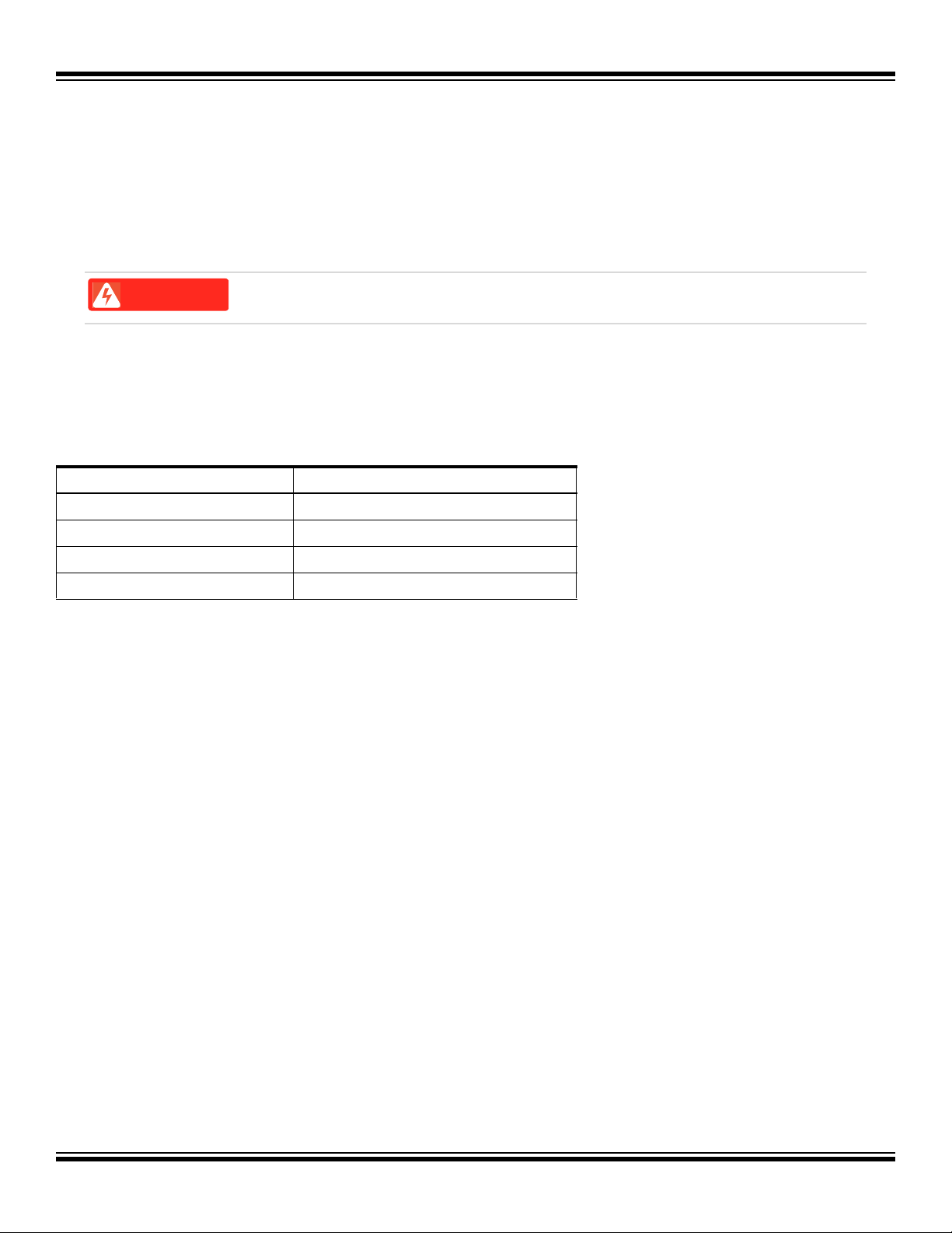
1. Evaluation Kit Specifications
Table 1-1: Evaluation Kit Specifications
Characteristic Specifications
Temperature
Relative Humidity 0 to 90% (non-condensing)
RoHS status Compliant
Ordering code ATSAMA5D3-XPLD
1.1 Electrostatic Warning
Operating 0°C to +70°C
Storage -40°C to +85°C
ESD-Sensitive Electronic Equipment!
The evaluation kit is shipped in a protective anti-static package. The board system must not be subject to high electrostatic potentials.
We strongly recommend using a grounding strap or similar ESD protective device when handling
the board in hostile ESD environments (offices with synthetic carpet, for example). Avoid touching
the component pins or any other metallic element on the board.
1.2 Power Supply Warning
Hardware Power Supply Limitation
Using a power adapter greater than 5Vcc (e.g. the 12Vcc power adapters from other kits such as
Arduino kits) may damage the board.
Hardware Power Budget
Using the USB as the main power source (max. 500 mA) is acceptable only with the use of the onboard peripherals and low-power LCD extension.
When external peripheral or add-on boards need to be powered, we recommend the use of an external power adapter connected to a J2 DC Jack (can provide up to 1.2A on the 3.3V node).
DS50002884A-page 2 2019 Microchip Technology Inc.
Page 3
SAMA5D3 XPLAINED
WARNING
2. Power-Up
Several power source options are available to power up the SAMA5D3 Xplained board.
The board can be:
• USB-powered through the USB Micro-AB connector (J6 connector - default configuration)
• Powered through an external AC-to-DC adapter connected via a 2.1 mm center-positive plug into the optional power jack of the
board. The recommended output voltage range of the power adapter is 5V at 2A.
• Powered through the Arduino shield
Unlike Arduino Uno boards, the SAMA5D3 Xplained board runs at 3.3V. The maximum voltage that
the I/O pins can tolerate is 3.3V. Providing higher voltages (e.g. 5V) to an I/O pin could damage the
board.
2.1 Power up the Board
Unpack the board, taking care to avoid electrostatic discharge. Simply connect the USB Micro-AB cable to the connector (J6).Then, connect the other end of the cable to a free USB port of your PC.
Table 2-1: Electrical Characteristics
Electrical Parameter Values
Input voltage 5 VCC
Maximum input voltage 6 VCC
Max DC 3.3V current available 1.2A
I/O Voltage 3.3V only
2.2 Sample Code and Technical Support
After booting up the board, you can run sample code or your own application on the board. You can download sample code and get technical support from the Microchip website.
®
software and demos can be found on the website Linux4SAM.
Linux
2019 Microchip Technology Inc. DS50002884A-page 3
Page 4

SAMA5D3 XPLAINED
3. Hardware Introduction
3.1 Introduction
The SAMA5D3 Xplained board is a fully-featured evaluation platform for Microchip SAMA5D3 series MPUs. It allows users to extensively
evaluate, prototype and create application-specific designs.
3.2 Equipment List
The SAMA5D3 Xplained board is built around the integration of a Cortex®-A5-based MPU (BGA 324 package) with external memory, dual
Ethernet physical layer transceiver, two SD/MMC interfaces, two host USB ports and one device USB port, one 24-bit RGB LCD interface
and one debug interface.
Seven headers, compatible with Arduino R3, are available for various shield connections.
DS50002884A-page 4 2019 Microchip Technology Inc.
Page 5

3.3 Board features
Table 3-1: Board Specifications
Characteristics Specifications
PCB characteristics 125 x 75 x 20mm (10-layers)
SAMA5D3 XPLAINED
Processor
Processor clock sources
Memory
Optional on-board memory
SD/MMC
USB
Display interface
Ethernet
Debug port
Expansion connectors
Board supply voltage
Battery On-board optional power Cap for CMOS backup
User interface
SAMA5D36 (324-ball BGA package) ARM Cortex-A5 Processor with ARM
v7-A Thumb2
12-MHz crystal oscillator
32.768-kHz crystal oscillator
2 x 1Gb DDR2 (16M x 16 bits x 8 banks)
1 x 2Gb SLC NAND Flash (256M x 8 bits)
One Serial EEPROM SPI
One 1-Wire EEPROM
One 8-bit SD card connector
One optional 4-bit Micro-SD card connector
Two USB Hosts with power switch
One Micro-AB USB device
One LCD interface connector, LCD TFT Controller with overlay, alphablending, rotation, scaling and color space conversion
One Gigabit Ethernet PHY (GRMII 10/100/1000)
One Ethernet PHY (RMII 10/100)
One JTAG interface connector
One serial DBGU interface (3.3V level)
Arduino R3 compatible set of headers
The SAMA5D36 GPIO,TWI, SPI, USART, UART, Audio and ISI interfaces
are accessible through these headers.
5V from USB or power jack or Arduino shield
On-board power regulation is performed by a Power Management Unit
(PMU)
Reset, wake-up and free user push button
One red user/power LED and one blue user LED
®
instruction set, core frequency up to 536 MHz.
2019 Microchip Technology Inc. DS50002884A-page 5
Page 6

SAMA5D3 XPLAINED
ATSAMA5D36
CU
1401 A
XXXXXXXXXX
ARM
J15 PIO Expansion
1Gb DDR2 Memory
1Gb DDR2 Memory
2Gb Nand Flash Memory
System Buttons
JTAG Interface
LCD Connector
Ethernet 10/100
GigaBit Ethernet
J18 PIO Expansion
Free User Push Button
ADC Inputs and CAN Interfaces
Debug Interface
SAMA5D36
Voltages and Reset Interface
ADC Inputs Expansion
Optional Supply Input
USB A Device
Supply Input
SPI Interface
J20 PIO Expansion
J19 PIO Expansion
XX
USB Host Interfaces
A
4. Board Components
4.1 Board Overview
The full-featured SAMA5D3 Xplained board integrates several peripherals and interface connectors, as shown in Figure 4-1.
Figure 4-1: SAMA5D3 Xplained Board Overview
ctor
DS50002884A-page 6 2019 Microchip Technology Inc.
Page 7

SAMA5D3 XPLAINED
The SAMA5D3 Xplained board is equipped with the interface connectors described in Table 4-1.
Table 4-1: SAMA5D3 Xplained Board Interface Connectors
Header Interfaces to
J2 Main power supply
J6 USB-A device. Supports USB device using a Micro-AB connector
J7 (upper) USB-B Host. Supports USB host using a type A connector
J7 (lower) USB-C™ Host. Supports USB host using a type A connector
J23 Serial DBGU 3.3V level
J24 JTAG, 20-pin IDC connector
J10 SD/MMC connector
J11 Micro-SD connector
J12 Gigabit Ethernet ETH0
J13 Ethernet ETH1
J22
C41 Optional SuperCap
Expansion connector with all LCD controller signals for display module connection (QTouch
display with Touch Screen and backlight
®
, TFT LCD
J14–J21 Expansion connectors with Arduino R3 compatible PIO signals
– Various test points located on the board
2019 Microchip Technology Inc. DS50002884A-page 7
Page 8

SAMA5D3 XPLAINED
JTAG
DBGU
JTAG & DBGU
SERIAL
DATA
Micro SD
CARD
10/100/1000
FAST ETHERNET
10/100
ETHERNET
SD
CARD
LCD
Connector
FLASH
ETH0
ETH1
PIO A,...EPIO A,...E
Single
PMU
Solution
5V INPUT
SAMA5D36
CORTEX®-A5 PROCESSOR
2Gb
DDR2
SDRAM
2Gb
NAND
FLASH
USB
DEVICE
USB
Host
x2
ANALOG Reference
VBAT
USER
LEDS
PIO
Expansion Headers
Power rails
USB A,B,C
Reset
Force PwrOn
Push
Buttons
EBI
5V & 3V3
(Up to 4Gb)
(Up to 4Gb)
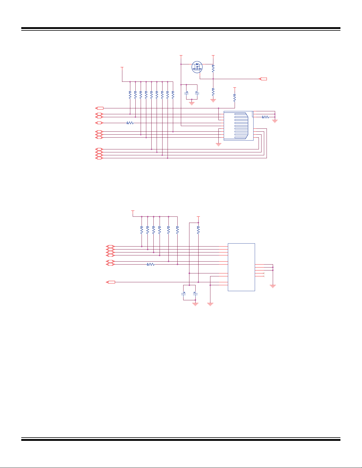
4.2 Function Blocks
Figure 4-2: Evaluation Kit Architecture
4.2.1 Processor
The SAMA5D3 Xplained board is built around the SAMA5D36, a Cortex-A5 application processor which combines high-performance computing device with low-power consumption and a wide range of communication peripherals. It features a combination of user interface
functionalities and high data rate IOs, including LCD controller, touchscreen, camera interface, Gigabit and 10/100 Ethernet ports, highspeed USB and SDIO.
The ARM Cortex-A5 supports the latest generation of DDR2 and NAND Flash memory interfaces for program and data storage. An internal
166-MHz multi-layer bus architecture associated with 24 DMA channels and two 64-Kbyte SRAM blocks, sustains the high bandwidth
required by the processor and the high-speed peripherals.
4.2.2 Clock Circuitry
The SAMA5D3 Xplained evaluation board features four clock sources:
• Two clocks are alternatives for the SAMA5D3 series processor main clock
• Two crystal oscillators are used for the GETH and Ethernet MII/RMII chip
Table 4-2: Main Components Associated with the Clock Systems
Quantity Description Component Assignment
1 Crystal for internal clock, 12 MHz Y1
1 Crystal for RTC clock, 32.768 kHz Y2
1 Oscillator for ethernet clock RGMII, 25 MHz Y3
1 Oscillator for ethernet clock RMII, 25 MHz Y4
DS50002884A-page 8 2019 Microchip Technology Inc.
Page 9

SAMA5D3 XPLAINED
WARNING
WARNING
4.2.3 Power Supplies
The on-board power supply generation is based on the Active-Semi® Power Management Unit (PMU) featuring a 3-channel (3.3V / 1.8V
/1.2V or 1.0V) topology. For maximum efficiency, these supply channels are generated by three integrated step-down converters.
In addition to these 3 DCDC channels, 4 LDO channels with low noise and high PSRR performance are available for the application. These
channels are disabled at startup by default and can be turned on and adjusted under software control through an I²C link. They are also
used to supply the 2.5V VDDFUSE and the 3.3V VDDANA power inputs of the processor.
The power supply sequencing of the three primary channels is controlled by the PMU itself in full compliance with the SAMAD3 requirements. The turn-on sequence is: 3.3V first, then 1.8V and finally 1.2V.
There is a known error on the ACT8865 I²C implementation. The port must be shut off after configuration or problems may occur with devices using the same I²C channel, e.g., TM43xx LCD display.
Refer to the ACT8865 data sheet at http://www.active-semi.com/ for more details.
This evaluation kit was equipped with an engineering version of ACT8865 PMIC known as
ACT8865QI303-T. The singularity of this engineering version is that OUT4 and OUT5 outputs, normally enabled at power-up, are disabled at power-up. Consequently, VDDANA and VDDFUSE
power inputs of the processor are OFF when the external reset pin (NRST) is released. They must
therefore be turned on by software in the very first execution steps of the application. In particular,
VDDFUSE is needed to switch SAMA5D3 devices in Secure mode.
The engineering version ACT8865QI303-T of the active semi PMIC is end-of-life (EOL) and replaced
by ACT8865QI305-T devices that have OUT4 and OUT5 enabled by default at power-up. Refer to
the following application note:
https://active-semi.com/wp-content/uploads/ActiveSemi_-ACT8865QI305T_versus_ACT8865QI303-T.pdf
Table 4-3 summarizes the power specifications.
Table 4-3: Supply Group Configuration
Nominal Name Power Domains Power Source
The slow clock oscillator, the internal
3.0V VDDBU
3.3V VDDIOP0 A part of peripheral I/O lines
3.3V VDDIOP1 A part of peripheral I/O lines
3.3V VDDUTMII The three USB interfaces
3.3V VDDOSC The main oscillator cells
3.3V VDDANA The analog-to-digital converter
1.2V VDDCORE
32K RC, the internal 12 MHz RC and a part
of the system controller
The core, including the processor, the
embedded memories and the peripherals
Optional on-board battery
PMU
2019 Microchip Technology Inc. DS50002884A-page 9
Page 10

SAMA5D3 XPLAINED
BP2
BP1
5V_MAIN
VDDCORE
VDDIOP1
VDDIOP0
VDDANA
VDDPLLA
VDDOSC
VDDIODDR
VDDIOM
AVDDL_PLL
DVDDL
AVDDL
FUSE_2V5
5V_MAIN
3V3
3V3
VDDUTMIC
3V3
TWCK_PMIC[7]
TWD_PMIC[7]
NRST
[5,9,10,11]
SHDN[5]
PC31
[7]
WKUP
[5]
PE30
[7]
(1V2)
(1V8)
(3V3)
(3V3)
(2V5)
RESETWAKUP or
Force Power ON
Auto
PWRON
(option)
PC27
PC26
C10
100nF
C10
100nF
L9 2.2uHL9 2.2uH
R14
50K
R14
50K
C21
2.2uF
C21
2.2uF
BP2BP2
C4
1uFC41uF
C13
10uF
C13
10uF
R16 0RR16 0R
C23
2.2uF
C23
2.2uF
R17 2R2R17 2R2
C20
100nF
C20
100nF
MN1 ACT8865MN1 ACT8865
GNDP129GNDA
2
INL45
5
VP1
31
INL67
6
GNDP2
28
VP2
26
GNDP314EXPAD
33
VP3
16
NC2
25
VDDREF
23
nRST0
11
nIRQ
12
nPBSTAT
13
VSEL
20
NC1
18
PWRHLD
10
PWREN
17
SCL
21
SDA
22
REFBP
32
nPBIN
9
SW1
30
OUT1
1
OUT2
24
SW2
27
SW3
15
OUT3
19
OUT4
3
OUT5
4
OUT6
7
OUT7
8
C2
4.7uFC24.7uF
JP1
DNP(JUMPER)
JP1
DNP(JUMPER)
1
2
Q1
IRLML2502Q1IRLML2502
1
3
2
C5
1uFC51uF
R19
100K 1%
R19
100K 1%
C1
4.7uFC14.7uF
R150RR15
0R
L11
180ohm at 100MHz
L11
180ohm at 100MHz
1 2
L8
180ohm at 100MHz
L8
180ohm at 100MHz
1
2
C18
47nF
C18
47nF
C22
2.2uF
C22
2.2uF
JP3 DNP(JUMPER)JP3 DNP(JUMPER)
1
2
R11 0RR11 0R
TP2
SMD
TP2
SMD
C26
4.7uF
C26
4.7uF
C6
1uFC61uF
R6
1.5K 1%R61.5K 1%
L5
2.2uHL52.2uH
JP4
DNP(JUMPER)
JP4
DNP(JUMPER)
1
2
C25
100nF
C25
100nF
L6
10uH60mAL610uH60mA
C3
4.7uFC34.7uF
JP2
DNP(JUMPER)
JP2
DNP(JUMPER)
1
2
R7
1.5K 1%R71.5K 1%
C11
4.7uF
C11
4.7uF
R5 2R2R5 2R2
R8
10KR810K
R41RR4
1R
C17
100nF
C17
100nF
C9
10uFC910uF
L7 2.2uHL7 2.2uH
C19
100nF
C19
100nF
L12
10uH60mA
L12
10uH60mA
C7
4.7uFC74.7uF
R186 0RR186 0R
L3
180ohm at 100MHz
L3
180ohm at 100MHz
1 2
L1
180ohm at 100MHz
L1
180ohm at 100MHz
1 2
R12 49.9K
L10
180ohm at 100MHz
L10
180ohm at 100MHz
1 2
C15
10uF
C15
10uF
TP1
SMD
TP1
SMD
C14
100nF
C14
100nF
R18 1KR18 1K
C130
10nF
C130
10nF
C16
10uF
C16
10uF
C8
10uFC810uF
R9 DNP(0R)R9 DNP(0R)
C24
2.2uF
C24
2.2uF
R13 0RR13 0R
R10 2R2R10 2R2
L4
10uH60mAL410uH60mA
L2
180ohm at 100MHz
L2
180ohm at 100MHz
1 2
BP1BP1
C12
10uF
C12
10uF
Table 4-3: Supply Group Configuration (Continued)
Nominal Name Power Domains Power Source
1.2V VDDUTMIC The USB UTMI + core
1.2V VDDPLLA The PLLA cell
1.8V VDDIODDR DDR2 interface I/O lines
1.8V VDDIOM
3.0V to
3.3V
ADVREF ADC reference voltage J15 header
NAND, NOR Flash and SMC interface I/O
lines
2.5V VDDFUSE Fuse box for programming PMU
Note: Jumper footprints are available on-board to measure power consumption on main power lines. By default, the jumpers are not
implemented. They are short-circuited by a thin PCB wire. To use this functionality, open the short circuit and mount a 2-pin
jumper.
Figure 4-3: Board Power Management Schematic
PMU
DS50002884A-page 10 2019 Microchip Technology Inc.
Page 11

SAMA5D3 XPLAINED
5V_MAIN
Vbus[5]
5V_Ext[11]
R175 0RR175 0R
J2
DNP(DC JACK)
J2
DNP(DC JACK)
3
1
2
R176 DNP(0R)R176 DNP(0R)
D4
P4SMAJ5.0A
D4
P4SMAJ5.0A
1 2
R3 DNP(0R)R3 DNP(0R)
R1 0RR1 0R
R2 DNP(0R)R2 DNP(0R)
R177 DNP(0R)R177 DNP(0R)
TDI
TMS
TCK
TDO
NTRST
NRST
VDDBU
3V3
3V3
TMS
[11]
TCK
[11]
TDO
[11]
TDI
[11]
NRST[4,9,10,11]
NTRST
[11]
VBat
[11]
(Super)-Capacitor
energy storage
Place TP4 to Bottom
Populate R185 if
no Super Cap (C41)
R25 10KR25 10K
R185
1.5K 1%
R185
1.5K 1%
D1
BAT54CLT1
D1
1 2
3
TP4
SMD
TP4
SMD
C27
10nF
C27
10nF
C28
100nF
C28
100nF
C41
DNP(0.2F/3V3)
C41
DNP(0.2F/3V3)
TDO
M11
TMS
N10
TCK
P9
NTRST
P11
TDI
R8
JTAGSEL
T9
BMS
U9
TST
U15
NRST
V9
VDDBU
V15
R23
1.5K 1%
R23
1.5K 1%
R21
100K 1%
R21
100K 1%
R22
DNP(100K)
R22
DNP(100K)
R20 100RR20 100R
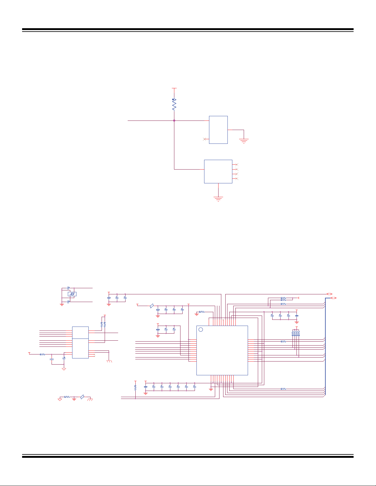
4.2.3.1 Power Options
Several power options are available to configure the SAMA5D3 Xplained board powering scheme.
The power sources are selected by a set of 0R resistors.
The USB-powered operation is the default configuration. The power source is the USB device port (J6) connected to a PC or a mini-AB
5V DC supply. The USB supply is sufficient to power the board in most applications if USB host ports are not used. If USB host ports are
used, it is recommended to use a DC supply source.
Schematic diagrams of various power options are illustrated in Figure 4-4.
Figure 4-4: Input Powering Scheme Option Schematic
Note: USB-powered operation is a good “single cable” solution because it combines powering and board control through a unique
cable. Consequently, it eliminates the need for other wires and batteries. This power option is suitable for most projects that
only require 5 volts at up to 500 mA.
4.2.3.2 Mains Power Adapter
A mains power supply adapter can be used to provide power to the board. A regulated 5V DC supply of typically 2A is required but a
current range of 3A is recommended if the USB ports and expansion headers are likely to be used. It needs a 2.1 mm plug with a centerhot configuration.
If you are using the USB host ports or expansion board Arduino shields, a higher current is required. To supply the full 500 mA per port,
a mains power adapter must be used.
4.2.3.3 VBAT
By default, VDDBU is delivered through the 3.3V node. An optional SuperCap (C41), used for real-time clock backup, is provided. The
board does not come equipped with the SuperCap. When the SuperCap is not installed, an R185 must be installed. You must make sure
that the R185 is removed prior to installing the SuperCap.
Figure 4-5: VBAT Powering Scheme Option Schematic
4.2.4 Reset Circuitry
The reset sources for the SAMA5D3 Xplained board are:
2019 Microchip Technology Inc. DS50002884A-page 11
Page 12

SAMA5D3 XPLAINED
DDR_A8
DDR_D9
DDR_D10
DDR_D11
DDR_D12
DDR_D13
DDR_D15
DDR_D14
DDR_A1
DDR_A9
DDR_A2
DDR_D2
DDR_A10
DDR_A3
DDR_A11
DDR_A4
DDR_A12
DDR_A5
DDR_D1
DDR_VREF
DDR_D0
DDR_A6
DDR_D4
DDR_D3
DDR_A7
DDR_D6
DDR_D5
DDR_D7
DDR_D8
DDR_A0
DDR_A8
DDR_D27
DDR_D26
DDR_D25
DDR_D31
DDR_D29
DDR_D28
DDR_D30
DDR_A1
DDR_A9
DDR_A2
DDR_A10
DDR_D18
DDR_A3
DDR_A11
DDR_A4
DDR_A12
DDR_A5
DDR_VREF
DDR_D17
DDR_D16
DDR_A6
DDR_D19
DDR_D20
DDR_D22
DDR_A7
DDR_D23
DDR_D21
DDR_D24
DDR_A0
DDR_DQM0
DDR_DQS1
DDR_DQS0
DDR_CS
DDR_BA0
DDR_BA1
DDR_BA2
DDR_CKE
DDR_WE
DDR_CLK
DDR_RAS
DDR_CLKN
DDR_CAS
DDR_DQM2
DDR_DQS2
DDR_DQS3
DDR_CS
DDR_BA0
DDR_BA1
DDR_BA2
DDR_WE
DDR_CKE
DDR_RAS
DDR_CLK
DDR_CAS
DDR_CLKN
DDR_A13
DDR_DQM1
DDR_DQM3
DDR_A13
VDDIODDR
VDDIODDR
VDDIODDR
VDDIODDR
DDR_A[0..13]
DDR_D[0..31]
C98
100nF
C98
100nF
C73 100nFC73 100nF
C100
100nF
C100
100nF
C68 100nFC68 100nF
R39 4.7KR39 4.7K
C93 100nFC93 100nF
C90 100nFC90 100nF
C69 100nFC69 100nF
R41 4.7KR41 4.7K
C91 100nFC91 100nF
C70 100nFC70 100nF
C97 100nFC97 100nF
MT47H64M16HR
DDR2 SDRAM
MN5
MT47H64M16HR
DDR2 SDRAM
MN5
A0
M8
A1
M3
A2
M7
A3
N2
A4
N8
A5
N3
A6
N7
A7
P2
A8
P8
A9
P3
A10
M2
BA0
L2
ODT
K9
DQ0
G8
DQ1
G2
DQ2
H7
DQ3
H3
DQ4
H1
DQ5
H9
DQ6
F1
DQ7
F9
UDQS
B7
UDQS
A8
LDM
F3
VDD
J9
VDD
M9
VDDL
J1
VREF
J2
VDDQ
E9
VSS
A3
VSS
E3
VDDQ
A9
VDD
E1
RFU1
A2
RFU2
E2
CKE
K2
CK
J8
CK
K8
CAS
L7
RAS
K7
WE
K3
CS
L8
VDDQ
C3
VDDQ
C7
VDDQ
C9
VSSQ
D8
VSSQ
E7
VSSQ
F2
VSSQ
F8
VDD
A1
VSS
J3
A11
P7
BA1
L3
A12
R2
BA2
L1
VSS
N1
VSSDL
J7
VSSQ
B2
RFU3
R3
DQ8
C8
DQ9
C2
DQ10
D7
DQ11
D3
DQ12
D1
DQ13
D9
DQ14
B1
DQ15
B9
VDD
R1
VDDQ
G1
VDDQ
G7
VDDQ
G9
VSS
P9
VSSQ
D2
VSSQ
A7
VSSQ
B8
VSSQ
H2
VSSQ
H8
VDDQ
G3
VDDQ
C1
UDM
B3
LDQS
E8
LDQS
F7
RFU4
R7
A13
R8
R40 4.7KR40 4.7K
C79 100nFC79 100nF
R36
DNP(1K)
R36
DNP(1K)
C71 100nFC71 100nF
R42 4.7KR42 4.7K
MT47H64M16HR
DDR2 SDRAM
MN4
MT47H64M16HR
DDR2 SDRAM
MN4
A0
M8
A1
M3
A2
M7
A3
N2
A4
N8
A5
N3
A6
N7
A7
P2
A8
P8
A9
P3
A10
M2
BA0
L2
ODT
K9
DQ0
G8
DQ1
G2
DQ2
H7
DQ3
H3
DQ4
H1
DQ5
H9
DQ6
F1
DQ7
F9
UDQS
B7
UDQS
A8
LDM
F3
VDD
J9
VDD
M9
VDDL
J1
VREF
J2
VDDQ
E9
VSS
A3
VSS
E3
VDDQ
A9
VDD
E1
RFU1
A2
RFU2
E2
CKE
K2
CK
J8
CK
K8
CAS
L7
RAS
K7
WE
K3
CS
L8
VDDQ
C3
VDDQ
C7
VDDQ
C9
VSSQ
D8
VSSQ
E7
VSSQ
F2
VSSQ
F8
VDD
A1
VSS
J3
A11
P7
BA1
L3
A12
R2
BA2
L1
VSS
N1
VSSDL
J7
VSSQ
B2
RFU3
R3
DQ8
C8
DQ9
C2
DQ10
D7
DQ11
D3
DQ12
D1
DQ13
D9
DQ14
B1
DQ15
B9
VDD
R1
VDDQ
G1
VDDQ
G7
VDDQ
G9
VSS
P9
VSSQ
D2
VSSQ
A7
VSSQ
B8
VSSQ
H2
VSSQ
H8
VDDQ
G3
VDDQ
C1
UDM
B3
LDQS
E8
LDQS
F7
RFU4
R7
A13
R8
C94 100nFC94 100nF
C78 100nFC78 100nF
C74 100nFC74 100nFR380RR38
0R
C95 100nFC95 100nF
C75 100nFC75 100nF
C96 100nFC96 100nF
R37 0RR37 0R
C88 100nFC88 100nF
C80 100nFC80 100nF
C89 100nFC89 100nF
C82 100nFC82 100nF
R35 DNP(1K)R35 DNP(1K)
C66 100nFC66 100nF
C83 100nFC83 100nF
C81 100nFC81 100nF
C84 100nFC84 100nF
C76 100nFC76 100nF
C86 100nFC86 100nFC85 100nFC85 100nF
C77 100nFC77 100nF
C67 100nFC67 100nF
C87 100nFC87 100nF
C92 100nFC92 100nF
C72 100nFC72 100nF
DDR_VREF
VDDIODDR
R46
1.5K 1%
R46
1.5K 1%
R451RR45
1R
R47
1.5K 1%
R47
1.5K 1%
C101
4.7uF
C101
4.7uF
TP3
SMD
TP3
SMD
L16
10uH60mA
L16
10uH60mA
C102
100nF
C102
100nF
C104
100nF
C104
100nF
C103
4.7uF
C103
4.7uF
• Power-on reset from the Power Management Unit (PMU),
• Reset Push button BP2,
• JTAG reset from an in-circuit emulator (through JTAG interface)
4.2.5 Memory Organization
The SAMA5D3x-series processor features a DDR2/SDRAM memory interface and an External Bus Interface (EBI) to interface with a wide
range of external memories and to almost any kind of parallel peripherals.
The memory devices that equip the SAMA5D3 Xplained evaluation kit are as follows:
• Two DDR2/SDRAM (MT47H64M16HR) used as main system memory (256 MByte). The board includes 2 Gbits of on-board soldered DDR2 (double data rate) SDRAM. The footprints can also host two DDR2 (MT47H128M16RT) from Micron
MBytes of DDR2 memory. The memory bus is 32 bits wide and operates with a frequency of up to 166 MHz (See Figure 4-6).
• One NAND Flash (MT29F2G08ABAEAWP) connected to the processor. The default size is 256 Mbytes. The footprint can also host
a 4-Gbit Micron chip for a total of 512 MBytes of NAND Flash memory (See Figure 4-7).
Figure 4-6: DDR2 Schematic
®
for a total of 512
DS50002884A-page 12 2019 Microchip Technology Inc.
Page 13

Figure 4-7: NAND Flash Schematic
NRD
NWE
M_EBI_D2
M_EBI_D4
M_EBI_D3
M_EBI_D6
M_EBI_D7
M_EBI_D5
M_EBI_D0
M_EBI_D1
NANDRDY
PE21
PE22
NCS3
VDDIOM
VDDIOM
(NANDCE)
(NANDCLE)
(NANDALE)
C105
100nF
C105
100nF
R48
100K 1%
R48
100K 1%
R50
100K 1%
R50
100K 1%
JP5
JUMPER
JP5
JUMPER
1
2
R49
100K 1%
R49
100K 1%
MN6
MT29F2G08ABAEAWP
MN6
MT29F2G08ABAEAWP
WE
18
N.C6
6
VCC
37
CE
9
RE
8
N.C11
20
WP
19
N.C5
5
N.C1
1
N.C2
2
N.C3
3
N.C4
4
DNU1
21
DNU2
22
N.C12
23
N.C13
24
R/B
7
I/O8_N.C
26
I/O9_N.C
27
I/O10_N.C
28
I/O0
29
VCC_N.C
34
N.C14
35
VSS
36
DNU3
38
VCC_N.C
39
VCC
12
VSS
13
ALE
17
N.C8
11
N.C7
10
N.C9
14
N.C10
15
CLE
16
VSS_N.C
25
I/O11_N.C
33
I/O1
30
I/O3
32
I/O2
31
I/O15_N.C
47
I/O14_N.C
46
I/O13_N.C
45
I/O7
44
I/O6
43
I/O5
42
I/O4
41
I/O12_N.C
40
VSS_N.C
48
C106
100nF
C106
100nF
The following memory part numbers are recommended:
Table 4-4: Recommended Memories
Part Number Supplier Size Type
MT47H128M16 Micron 2 Gb (
16 M x 16 x 8 banks) DDR2 - BGA
SAMA5D3 XPLAINED
MT47H128M32 Micron 4 Gb (32
M x 16 x 8 banks) DDR2 - BGA
MT29F2G08 Micron 2 Gb NAND Flash - TSOP
MT29F4G08 Micron 4 Gb NAND Flash - TSOP
4.2.6 SD/MMC Interface
The SAMA5D3 Xplained board features two high-speed Multimedia Card Interfaces (MCI).
• The first interface is used as an 8-bit interface (MCI0), connected to a SD/MMC card slot (J10) located on the bottom side of the
PCB.
• The second interface is used as a 4-bit interface (MCI1), connected to an optional Micro-SD card connector (J11) located on the top
side of the PCB.
The MCI0 SD card power line is enabled by default. It is PIO-controlled through a MOSFET transistor.
Note: The power source is VCC (3.3 volts).
4.2.6.1 J10 SD Card Slot
When a card is inserted into the SD/MMC connector, the Card Detect pin (PE0) is tied to ground.
2019 Microchip Technology Inc. DS50002884A-page 13
Page 14
SAMA5D3 XPLAINED
VDDIOP1
VDD_MCI0
VDDIOP1
VDDIOM
PD1[7]
PE2 [7]
PD9[7]
PD0
[7]
PD4[7]
PD3[7]
PE0[7]
PD6[7]
PD7[7]
PD8[7]
PD5[7]
PD2[7]
(MCI0_CD)
(MCI0_WP)
(MCI0_DA1)
(MCI0_DA0)
(MCI0_CK)
(MCI0_CDA)
(MCI0_DA3)
(MCI0_DA2)
(MCI0_DA4)
(MCI0_DA5)
(MCI0_DA7)
(MCI0_DA6)
C108
10uF
C108
10uF
R55
DNP(4.7K)
R55
DNP(4.7K)
R12268K R12268K
R182 22RR182 22R
R12768K R12768K
J10
7SDMM-B0-2211
J10
7SDMM-B0-2211
8
5
7
6
4
3
2
1
9
14
15
16
13
12
11
10
R5410K R5410K
R12468K R12468K
R53
100K 1%
R53
100K 1%
R57 0RR57 0R
R12668K R12668K
R12168K R12168K
Q3
IRLML6402
Q3
IRLML6402
1
3
2
R12368K R12368K
R56
10K
R56
10K
R12868K R12868K
C109
100nF
C109
100nF
R12568K R12568K
Figure 4-8: J10 SD Card Schematic
4.2.6.2 J11 SD Card Slot (optional)
When a card is inserted into the Micro SD connector, the Card Detect pin is tied to ground. This is detected on pin PE1 of the main processor.
Figure 4-9: J11 Micro SD Card Schematic
VDDIOP1
VDDIOM
R12968K R12968K
R13268K R13268K
R5810K R5810K
R112DNP(68K) R112DNP(68K)
C110
C110
10uF
10uF
C111
C111
100nF
100nF
R59
R59
10K
10K
7
DAT0
8
DAT1
1
DAT2
2
DAT3
3
CMD
5
CLK
4
VDD
6
VSS
9
CD
10
PGND
J11
J11
PGND
PGND
PGND
DNP(MCTF-0403)
DNP(MCTF-0403)
11
12
13
14
NC
15
NC
R13068K R13068K
R13168K R13168K
PB20[7]
PB21[7]
PB22[7]
PB23[7]
PB19[7]
PB24
[7]
PE1[7]
(MCI1_DA0)
(MCI1_DA1)
(MCI1_DA2)
(MCI1_DA3)
(MCI1_CDA)
(MCI1_CK)
(MCI1_CD)
R183 22RR183 22R
Micro SD CARD INTERFACE - MCI1
4.2.7 Serial Peripheral Interface (SPI)
The SAMA5D3X-series processor features two high-speed Serial Peripheral Interfaces. One port is used to interface with the optional onboard serial DataFlash®.
There are four main signals used in the SPI interface; Clock, Data In, Data Out, and Chip Select.
DS50002884A-page 14 2019 Microchip Technology Inc.
Page 15

Figure 4-10: Optional Serial DataFlash Schematic
VDDIOP1
R52
R52
100K 1%
100K 1%
PD11
PD10
PD12
PD13
(SPI0_MOSI)
(SPI0_MIS0)
(SPI0_SPCK)
(SPI0_CS)
1
2
JP6
JP6
JUMPER
JUMPER
MN8
MN8
5
DQO
2
DQ1
6
C
W/Vpp/DQ2
HOLD/DQ3
1
S
DNP(N25Q032A13ESE40F)
DNP(N25Q032A13ESE40F)
VCC
GND
8
3
7
4
SAMA5D3 XPLAINED
VDDIOP1
C107
C107
100nF
100nF
2019 Microchip Technology Inc. DS50002884A-page 15
Page 16
SAMA5D3 XPLAINED
PB3
PB2
PB1
PB0
PB4
PB5
PB6
PB7
ETH0_A+
ETH0_A-
ETH0_BETH0_C+
ETH0_C-
ETH0_D+
ETH0_D-
PB16
PB11
PB13
PB9
PB17
PB10
ETH0_LED2
XI
XO
ETH0_LED1
XI
XO
PB18
PB8
ETH0_B+
VDDIOP1
DVDDL
AVDDL
AVDDH
AVDDL_PLL
VDDIOP1
VDDIOP1
VDDIOP1
VDDIOP1
PB[0..31]
[7,8,10,11]
NRST [4,5,10,11]
G125CK
GTX0
GTX1
GTX2
GTX3
GRX0
GRX1
GRX2
GRX3
GTXCK
GTX_CTL
GRXCK
GRX_CTL
GMDC
GMDIO
INT_GETHR
10Base-T/100Base-TX/1000BASE-T
R64
4.7K
R64
4.7K
R68 22RR68 22R
+
C127
10uF
+
C127
10uF
C112 20pFC112 20pF
R61 1KR61 1K
C120
10nF
C120
10nF
R67
4.7K
R67
4.7K
C136
10nF
C136
10nF
+
C113
10uF
+
C113
10uF
Y3
25MHzY325MHz
1
23
4
C121
10nF
C121
10nF
C135
10nF
C135
10nF
C129
10nF
C129
10nF
+
C126
10uF
+
C126
10uF
C116 20pFC116 20pF
R69
4.7K
R69
4.7K
C119
10nF
C119
10nF
L17
180ohm at 100MHz
L17
180ohm at 100MHz
1 2
C122
10nF
C122
10nF
C115
10nF
C115
10nF
R65
4.7K
R65
4.7K
C134
10nF
C134
10nF
C128
10nF
C128
10nF
C118
10nF
C118
10nF
C114
10nF
C114
10nF
C133
10nF
C133
10nF
C123
10nF
C123
10nF
KSZ9031RNI
48-pin QFN
MN10
KSZ9031RN
KSZ9031RNI
48-pin QFN
MN10
KSZ9031RN
VSS_PS13LED215DVDDH16LED117DVDDL14TXD019TXD120TXD221TXD322DVDDL18DVDDL23GTX_CLK
24
TX_EN
25
DVDDL
26
RXD3
27
VSS
29
DVDDL
30
RXD1
31
RXD0
32
RX_DV
33
DVDDH
34
RX_CLK
35
MDC
36
MDIO
37
INT_N
38
DVDDL
39
DVDDH
40
CLK125_NDO
41
RESET_N
42
LDO_O
43
XO
45
XI
46
AVDDH
47
ISET
48
AVDDH
1
TXRXP_A
2
TXRXM_A
3
TXRXP_B
5
TXRXM_B
6
TXRXP_C
7
TXRXM_C
8
TXRXP_D
10
TXRXM_D
11
AVDDH
12
RXD2
28
AVDDL_PLL
44
P_GND
49
AVDDL
4
AVDDL
9
R66
4.7K
R66
4.7K
R63 12.1K 1%R63 12.1K 1%
C138
10nF
C138
10nF
R60 4.7KR60 4.7K
+
C117
10uF
+
C117
10uF
C137
10nF
C137
10nF
R70 22RR70 22R
+
C132
10uF
+
C132
10uF
R62 22RR62 22R
EARTH_ETH0
ETH0_GND
R73 0RR73 0R
L18 180ohm at 100MHzL18 180ohm at 100MHz
1
2
ETH0_B+
ETH0_B-
ETH0_D+
ETH0_D-
ETH0_A+
ETH0_A-
ETH0_C+
ETH0_C-
ETH0_LED1
ETH0_LED2
AVDDH
VDDIOP1
EARTH_ETH0
ETH0_GND
LINK
ACT
Left Green LED
Right Yellow LED
C124
100nF
C124
100nF
R71470R R71470R
J12
48F-01GY2DPL2NL
J12
48F-01GY2DPL2NL
TD2+
3
TD1+
1
TD1-
2
TD3+
7
TD3-
8
RCT
6
TD2-
4
GRLA
11
GRLC
12
TD4+
9
TD4-
10
TCT
5
YELC
13
YELA
14
GND
15
GND
16
GND
17
GND
18
R72470R R72470R
R111 DNP(0R)R111 DNP(0R)
C125
DNP(10uF 0805)
C125
DNP(10uF 0805)
4.2.8 Optional 1-Wire EEPROM
The SAMA5D3 Xplained board can use a 1-Wire device as “soft label” to store data such as chip type, manufacturer’s name, production
date, etc.
Figure 4-11: Optional One-Wire EEPROM Schematic
VDDIOM
R51
R51
1.5K
1.5K
MN11
PE23
MN11
1
IO
2
NC
DNP(DS28E05)
DNP(DS28E05)
2
IO
GND
MN7
MN7
NC1
NC2
NC3
NC4
GND
1
DNP(DS2431)
DNP(DS2431)
3
3
4
5
6
4.2.9 10/100/100 Ethernet Port
The SAMA5D3 Xplained board features a MICREL PHY device (KSZ9031RN) operating at 10/100/1000 Mb/s. The board supports the
RGMII Interface mode. The Ethernet interface consists of four pairs of low-voltage differential pair signals designated from GRX± and
GTX± plus Control signals for link activity indicators. These signals are routed to the 10/100/1000BASE-T RJ45 connector (J12).
For monitoring and control purposes, LEDs are integrated in the RJ45 connectors to indicate activity, link, and speed status information
for the corresponding ports.
For more information about the Ethernet controller device, refer to the MICREL KSZ9031RN data sheet.
Figure 4-12: Gigabit Ethernet Schematic
DS50002884A-page 16 2019 Microchip Technology Inc.
Page 17

SAMA5D3 XPLAINED
4.2.10 Ethernet 10/100 Port
The SAMA5D3 Xplained board features a MICREL PHY device (KSZ8081RNB) operating at 10/100 Mb/s. The board supports RMII interface modes. The Ethernet interface consists of two pairs of low-voltage differential pair signals designated from GRX± and GTX± plus
Control signals for link activity indicators. These signals are routed to the 10/100BASE-T RJ45 connector (J13).
For monitoring and control purposes, an LED functionality is added on the RJ45 connectors to indicate activity, link, and speed status
information for the corresponding ports.
For more information about the Ethernet controller device, refer to the MICREL KSZ8081RNB controller manufacturer's data sheet.
Figure 4-13: RMII Ethernet Schematic
VDDIOP1 VDDIOP0
L19
L19
1 2
+
+
C144
C144
10uF
10uF
+
+
C146
C146
10uF
10uF
R741KR74
1K
VDDIOP0
180ohm at 100MHz
180ohm at 100MHz
NRST [4,5,9,11]
EARTH_ETH1
VDDIOP0
13
14
15
16
R79 470RR79 470R
R80 470RR80 470R
1
TX+
1
TX+
2
TX-
2
TX-
3
RX+
3
RX+
6
RX-
6
RX-
4
4
5
5
7
7
8
8
12
R81 0RR81 0R
10Base-T/100Base-TX
MN9
J1313F-64GYD2PL2NL
J1313F-64GYD2PL2NL
TD+
TD+
1
CT
CT
4
TD-
TD-
2
RD+
RD+
3
CT
CT
5
RD-
RD-
6
C139
C139
100nF
NC
NC
7
8
9
180ohm at 100MHz
180ohm at 100MHz
100nF
GND_ETH1
EARTH_ETH1
75 75
75 75
75
75
1nF
1nF
75
75
Left Green LED Right yellow LED
Left Green LED Right yellow LED
10
11
VDDIOP0
+
+
C148
C148
10uF
10uF
L20
L20
1 2
EARTH_ETH1GND_ETH1
C140
C140
100nF
100nF
ETH1_LED0
TX-
RX+
RX-
ACT
LINK
ETH1_LED0
ETH1_LED1ETH1_LED1
C147 20pFC147 20pF
C149
C149
20pF
20pF
23
VDDIOP0
R77
R77
10K
10K
1
4
25MHzY425MHz
Y4
R78
R78
10K
10K
ETH1_XI
ETH1_XO
TX+TX+
TX-
RX+
RX-
C141 2.2uFC141 2.2uF
C142 100nFC142 100nF
7
TXP
6
TXM
5
RXP
4
RXM
2
VDD_1V2
1
GND
33
PADDLE
22
TXC
26
TXD2
27
TXD3
R766.49k/1% R766.49k/1% C143
10
REXT
ETH1_XO
8
XO
ETH1_XI
9
XI
30
LED0/NWAYEN
31
LED1/SPEED
RXC/B-CAST_OFF
TXD1
TXD0
TXEN
RXD3/PHYAD0
RXD2/PHYAD1
RXD1/PHYAD2
RXD0/DUPLEX
RXDV/CONFIG2
RXER/ISO
CRS/CONFIG1
COL/CONFIG0
MDIO
INTRP/NAND
VDDA_3V3
VDDIO
RESET
KSZ8081RNB
KSZ8081RNB
MN9
19
25
24
23
13
14
15
16
18
20
29
28
12
MDC
11
21
E1_AVDDT
3
C143
100nF
100nF
17
C145
C145
100nF
100nF
32
4.2.11 Indicators
Two LEDs are available on the SAMA5D3 Xplained board. Both can be software-controlled by the user.
• The red LED indicates that power is applied to the board (by default). It can be controlled via software.
• The blue LED is mainly controlled by one GPIO line.
R751KR75
1K
R114
R114
R115
R115
R113
R113
10K
10K
10K
10K
10K
10K
R116
R116
R120
R120
R117
R117
R118
R118
R119
R119
10K
10K
10K
10K
10K
10K
10K
10K
10K
10K
ETH1_PC7 [7]
ETH1_PC1 [7]
ETH1_PC0 [7]
ETH1_PC4 [7]
ETH1_PC3 [7]
ETH1_PC2 [7]
ETH1_PC5 [7]
ETH1_PC6 [7]
ETH1_PC8 [7]
ETH1_PC9 [7]
PB12 [7]
Figure 4-14: LED Indicators Schematic
R32
PE[0..31][4,7,8,11]
PE23
PE24
1
Q2
Q2
IRLML2502
IRLML2502
R32
R33 100K 1%R33 100K 1%
32
470R
470R
R34
R34
470R
470R
2019 Microchip Technology Inc. DS50002884A-page 17
D2
BLUED2BLUE
D3
REDD3RED
3V3
LED
Page 18
SAMA5D3 XPLAINED
HHSDPC
HHSDMA
HHSDPA
HHSDMB
HHSDPB
HHSDMC
HHSDMC
HHSDPC
HHSDMB
HHSDPB
5V_USBB
5V_USBC
5V_USBB
5V_USBC
GNDUTMI
GNDUTMI
EARTH_USB
5V_MAIN
EARTH_USB
EARTH_USB_A
PE5 [7]
Vbus[4]
PE9
[7,11]
PE4 [7]
PE3 [7]
OVCUR_USB
USB A DEVICE INTERFACE
(VBUS_SENSE)
J7_USB_A_Up J7_USB_B_Down
EN5V_USBC
EN5V_USBB
C60
10pF
C60
10pF
32.768K
R27
200K
R27
200K
20pF20pF
p
p
MN3
SP2526A-2E
MN3
SP2526A-2E
ENA
1
FLGA
2
ENB
4
OUTA
8
GNG6FLGB
3
IN
7
OUTB
5
J6
UBAF-1015P
J6
UBAF-1015P
MN2H
SAMA5D3x_BGA324
MN2H
SAMA5D3x_BGA324
GNDCORE_1
A
A
GNDCORE_2
GNDIODDR_1
GNDIODDR_2
GNDIODDR_3
GNDIODDR_4
GNDIODDR_5
GNDIOP_1
GNDIOM_1
GNDANA
L4
ADVREF
VDDANA
GNDIOP_2
GNDCORE_3
GNDFUSE
GNDPLL
GNDUTMI_1
R12
VDDPLLA
VBG
R11
GNDCORE_4
GNDOSC
GNDBU
GNDCORE_5
GNDIOM_2
GNDIOP_3
VDDOSC
VDDUTMII
XIN32
U16
XOUT
V8
VDDUTMIC
XOUT32
V16
GNDCORE_6
GNDIOP_4
HHSDMA
V10
HHSDPA
U10
HHSDMC
V14
HHSDPC
U14
HHSDPB
U12
HHSDMB
V12
DIBN
U6
DIBP
V6
C61
100nF
C61
100nF
L21 180ohm at 100MHzL21 180ohm at 100MHz
1
2
20
20pF
12MHz
C64
100nF
C64
100nF
R30
5.62K 1%
R30
5.62K 1%
L13
180ohm at 100MHz
L13
180ohm at 100MHz
1 2
C62
10uF
C62
10uF
C63
100nF
C63
100nF
L15
180ohm at 100MHz
L15
180ohm at 100MHz
1 2
A
B
J7
Dual USB A
A
B
J7
Dual USB A
5
8
6
7
9
10
1
2
3
4
11
12
R31 0RR31 0R
20pF20pF
p
p
L14
180ohm at 100MHz
L14
180ohm at 100MHz
1 2
C65
10uF
C65
10uF
R26 100K 1%R26 100K 1%
EARTH_USB_A
VBUS
DM
DP
ID
GND
VBUS
DM
DP
ID
GND
1
2
3
4
5
76
8
4.2.12 USB
The SAMA5D3 Xplained board features three USB communication ports:
• Port A: High-speed (EHCI) and full-speed (OHCI) host multiplexed with high-speed USB device Micro-AB connector (J6)
• Port B: High-speed (EHCI) and full-speed (OHCI) host, standard type A connector (J7 upper port)
• Port C: Full-speed OHCI host, standard type A connector (J7 lower port)
The two USB host ports are equipped with 500-mA high-side power switch for self-powered and bus-powered applications.
The USB device port A (J6) features a VBUS insert detection function through the ladder-type resistors R26 and R27.
Figure 4-15: USB Interface Schematic
Y
pF
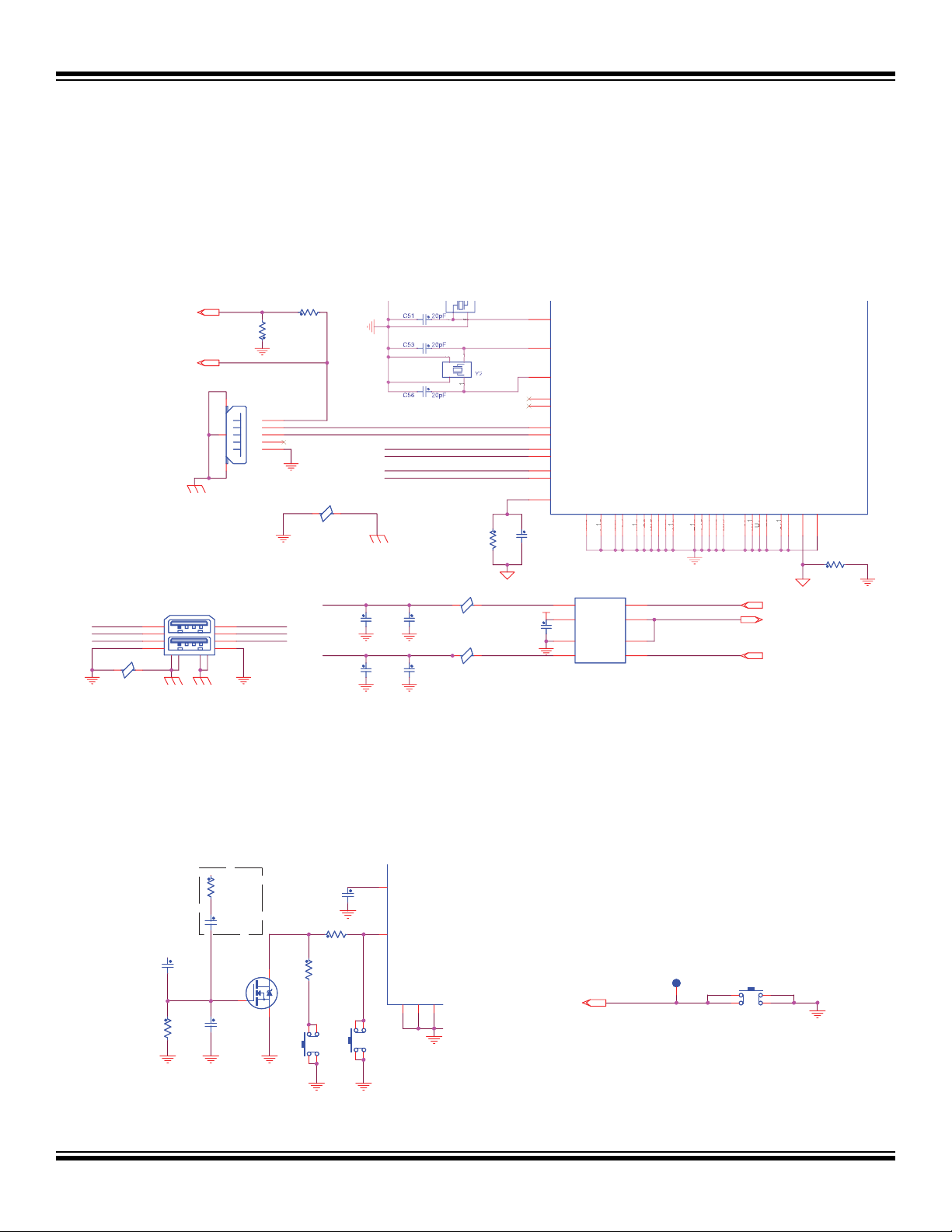
4.2.13 Push Button Switches
The following push button switches are available:
• One board reset button (BP2). When pressed and released, this push button causes a Power-on Reset of the whole board.
• One wake-up push button that brings the processor out of Low-Power mode (BP1)
• One user push button (BP3)
Figure 4-16: Push Button Schematic
C25
C25
100nF
100nF
R19
R19
C130
C130
10nF
100K 1%
100K 1%
WAKUP or Force Power ON
DS50002884A-page 18 2019 Microchip Technology Inc.
10nF
R14
R14
50K
50K
C20
C20
100nF
100nF
IRLML2502
IRLML2502
Auto
PWRON
(option)
Q1
Q1
3
1
2
R12 49.9K
R150RR15
0R
BP1
BP1BP1
C18
C18
47nF
47nF
BP2
BP2BP2
32
REFBP
9
nPBIN
RESET
GNDP129GNDA2GNDP2
28
TP5
TP5
SMD
SMD
[7,11]
PE29
Place TP5 to Bottom
USER BUTTON
BP3BP3
Page 19

SAMA5D3 XPLAINED
4.2.14 LCD
The SAMA5D36 processor drives 24 bits of Data and Control signals to the LCD interface. Other signals are used to control the LCD and
are also routed to the J22 connector: TWI, SPI, 2 GPIOs for interrupt, ID for 1-Wire EEPROM (ID_SYS) and power supply lines.
4.2.14.1 LCD Connector
One 1.27 mm pitch 50-pin header is provided to gain access to the LCD signals.
Figure 4-17: LCD Expansion Header Interface Schematic
3V3
5V_MAIN
DNP(0R)
DNP(0R)
R92
R92
See
Errata section
NRST
PE6
PD20
PD12
PD21
PD11
PD22
PD10
PD23
PD16
PA28
TWCK_LCD[7]
TWD_LCD[7]
(RST_LCD)
(AD0)
(SPI0_SPCK)
(AD1)
(SPI0_MOSI)
(AD2)
(SPI0_MISO)
(AD3)
(SPI0_NPCS3)
(LCDPCK)
R93 0RR93 0R
R94 0RR94 0R
R99 DNP(0R)R99 DNP(0R)
R95 DNP(0R)R95 DNP(0R)
R96 22RR96 22R
DNP(0R)
DNP(0R)
R100
R100
R97 22RR97 22R
R98
R98
DNP(0R)
DNP(0R)
R101 22RR101 22R
DNP(0R)
DNP(0R)
R102
R102
R103 22RR103 22R
R184 22RR184 22R
TWCK_LCD
TWD_LCD
LCD Connector
(LCDPWM)
PA24
(IRQ2)
PE8
IRQ1)
PE7
TWCK_LCD
TWD_LCD
(LCDDISP)
PA25
(LCDDEN)
PA29
PA27
(LCDHSYNC)
(LCDVSYNC)
PA26
(LCDDAT23)
PE28
(LCDDAT22)
PE27
(LCDDAT21)
PC15
(LCDDAT20)
PC10
(LCDDAT19)
PC11
(LCDDAT18)
PC12
(LCDDAT17)
PC13
(LCDDAT16)
PC14
(LCDDAT15)
PA15
(LCDDAT14)
PA14
(LCDDAT13)
PA13
(LCDDAT12)
PA12
PA11
(LCDDAT11)
PA10
(LCDDAT10)
PA9
(LCDDAT9)
PA8
(LCDDAT8)
PA7
(LCDDAT7)
PA6
(LCDDAT6)
PA5
(LCDDAT5)
PA4
(LCDDAT4)
PA3
(LCDDAT3)
PA2
(LCDDAT2)
(LCDDAT1)
PA1
(LCDDAT0)
PA0
PE23
(ID_SYS)
J22J22
50
49
48
47
46
45
44
43
42
41
40
39
38
37
36
35
34
33
32
31
30
29
28
27
26
25
24
23
22
21
20
19
18
17
16
15
14
13
12
11
10
9
8
7
6
5
4
3
2
1
FP520T1-50SR04
52
51
4.2.14.2 LCD Power
To operate correctly with various LCD modules, regardless of the processor, two voltage lines are available: 3V3 by default and 5V_MAIN,
both selected by 0R resistors R92 and R93.
4.2.15 Debug JTAG/ICE and DBGU
4.2.15.1 Debug JTAG/ICE
A 2x10-pin JTAG header is implemented on the SAMA5D3 Xplained board to enable the software development and debugging of the
board by using various JTAG emulators. The interface signals have a voltage level of 3.3V.
2019 Microchip Technology Inc. DS50002884A-page 19
Page 20

SAMA5D3 XPLAINED
Figure 4-18: JTAG/ICE Interface Schematic
JTAG
3V3
J24J24
2
6
8
10
12
14
16
18
20
R104
R104
100K 1%
100K 1%
1
34
TDI
5
TMS
7
TCK
9
11
13
15
17
19
RTCK
TDO
R109 0RR109 0R
R110 0RR110 0R
R105
R105
100K 1%
100K 1%
VDDIOP0
R106
R106
100K 1%
100K 1%
R107
R107
100K 1%
100K 1%
R108 0RR108 0R
NTRST [5]
TDI [5]
TMS [5]
TCK [5]
TDO [5]
NRST [4,5,9,10]
4.2.15.2 DBGU
The SAMA5D3 Xplained board has a dedicated serial port for debugging, which is accessible through the 6-pin male header J23. Various
interfaces can be used as USB/Serial DBGU port bridge, such as FTDI TTL-232R-3V3 USB to TTL serial cable or basic breakout board
for the 232/USB converter.
These interfaces are available on the following websites:
• Adafruit: http://www.adafruit.com/products/284
•Sparkfun: https://www.sparkfun.com/products/9873
Figure 4-19: DBGU Interface Schematic
5V_MAIN
3V33V3
R189
R190
R171DNP(0R)
R172DNP(0R)
68K
68K
PE13
[7]
PB31
[7]
PB30
PE14
R173 0R
(TXD)
(RXD)
R174 0R
J23
1
2
3
4
5
6
DEBUG
P101-1*06SGF-116A-NX
R171 and R172 are optional (not implemented) resistors that can be used for power selection. Power can be delivered either by the
SAMA5D3 Xplained board or by the debug interface tool. To avoid a contention between your debug interface (e.g. FTDI) and the onboard power system, be careful during the installation of one of these resistors.
4.2.16 Expansion Ports
Five 8-pin, one 10-pin, one 6-pin and one 2x18-pin headers (J14 to J21) are implemented on the board to enable the PIO connection of
various expansion cards that could be developed by users or by other sources. Due to multiplexing, different signals can be provided on
each pin. These connectors are mechanically- and footprint- compatible with the Arduino R3 shields. As the SAMA5D3 signals have a
voltage level of 3.3V, 5-V level shields must not be used on the SAMA5D3 Xplained.
In addition to its standard IO functionality, the SAMA5D3 processor can provide alternate functions to external IO lines available on the
J14 to J21 headers.
These alternate functions are:
• UARTs: UART0, UART1
• USARTs: USART0, USART1, USART2, USART3
• SPI: SPI1
DS50002884A-page 20 2019 Microchip Technology Inc.
Page 21

SAMA5D3 XPLAINED
• I²C: TWI0, TWI1
• Timer capture and compare: TIOA, TIOB
• Clock out: PCK0, PCK1, PCK2
• PWMs: PWML0, PWMH0, PWML1, PWMH1
• DIGITAL AUDIO: TD0, TK0, TF0, RD0, RK0, RF0
• ISI: ISI[D0:D11], ISI_HSYNC, ISI_VSYNC, ISI_PCK
• CAN: CAN-RX0, CANTX0, CANRX1, CAN_TX1
• Analog: AD[0:11], ADTRG, ADREF
• GPIO: MISC
• RESET
• VBAT
Refer to the SAMA5D3 series data sheet for further details on the PIO multiplexing and alternate function selection.
2019 Microchip Technology Inc. DS50002884A-page 21
Page 22

SAMA5D3 XPLAINED
4.2.16.1 Functions Available Through the Arduino Headers
The following tables illustrate the functionalities provided by the SAMA5D3 Xplained board. They show the pins used to implement each
functionality.
Note: Some pins are multiplexed for different functionalities, which means that only one at a time can be active for each pin.
Table 4-5: Function by PIO (Part 1)
PIO NAME PCK ISI SSC CAN SPI
PC16 -- -- TK0 -- --
PC17 -- -- TF0 -- --
PC18 -- -- TD0 -- --
PC20/PD28 -- -- RF0 -- --
PC21/PD29 -- -- RD0 -- --
PC19/PD30 PCK0 -- RK0 -- --
PD30/PC15 PCK0/PCK2 -- -- -- --
PD31 PCK1 -- -- -- --
PB14------CANRX1--
PD14 -- -- -- CANRX0 --
PB15 -- -- -- CANTX1 --
PD15 -- -- -- CANTX0 --
PC22/PC1 -- -- -- -- SPI1_MISO
PC24/PC0 -- -- -- -- SPI1_SPCK
PC23/PC2 -- -- -- -- SPI1_MOSI
PC25 -- -- -- -- SPI1_NPCS0
PC26/PA30 -- ISI_D11/VSYNC -- -- SPI1_NPCS1
PC27/PA31 -- ISI_D10/HSYNC -- -- SPI1_NPCS2
PC28 -- ISI_D9 -- -- SPI1_NPCS3
PC29 -- ISI_D8 -- -- --
PA23 -- ISI_D7 -- -- --
PA22 -- ISI_D6 -- -- --
PA21 -- ISI_D5 -- -- --
PA20 -- ISI_D4 -- -- --
PA19 -- ISI_D3 -- -- --
PA18 -- ISI_D2 -- -- --
PA17 -- ISI_D1 -- -- --
PA16 -- ISI_D0 -- -- --
PC30 -- ISI_PCK -- -- --
PA30 -- ISI_VSYNC -- -- --
PA31 -- ISI_HSYNC -- -- --
DS50002884A-page 22 2019 Microchip Technology Inc.
Page 23

SAMA5D3 XPLAINED
Table 4-6: Function by PIO (Part 2)
PIO NAME TWI UART/USART ANALOG MISC
3V3/5V -- -- -- 3V3/5V
nRTS -- -- -- nRTS
GND ------GND
AREF -- -- AREF --
5V -- -- -- 5V
PC18 -- -- AD0 --
PD21 -- -- AD1 --
PD22 -- -- AD2 --
PD23 -- -- AD3 --
PD24 -- -- AD4 --
PD25 -- -- AD5 --
PD26 -- -- AD6 --
PD27 -- -- AD7 --
PC20/PD28 -- -- AD8 --
PC21/PD29 -- -- AD9 --
PC19/PD30 -- -- AD10 --
PD31 -- -- AD11 --
PD19/PB15 -- -- ADTRG --
PA1 9 TWC K2 - - -- --
PA18 TWD2 -- -- --
PC26 TWD1 -- -- --
PA30 TWD0 URXD1 -- --
PA31 TWCK0 UTXD1 -- --
PC26/PA30 TWD0/TWD1 URXD1 -- --
PC27/PA31 TWCK0/TWCK1 URTD1 -- --
PC30 -- UTXD0 -- --
PC29 -- URXD0 -- PWMFI2
PD14 -- SCK0 -- --
PD15 -- CTS0 -- --
PD18 -- TXD0 -- --
PD17 -- RXD0 -- --
PB25 -- SCK1 -- --
PB26 -- CTS1 -- --
PB29 -- TXD1 -- --
PB28 -- RXD1 -- --
2019 Microchip Technology Inc. DS50002884A-page 23
Page 24

SAMA5D3 XPLAINED
Table 4-6: Function by PIO (Part 2) (Continued)
PIO NAME TWI UART/USART ANALOG MISC
PB27 -- RTS1 -- PWMH1
PE20 -- SCK2 -- --
PE23 -- CTS2 -- --
PE26 -- TXD2 -- --
PE25 -- RXD2 -- --
PE24 -- RTS2 -- --
PE15 -- SCK3 -- --
PE16 -- CTS3 -- --
PE19 -- TXD3 -- --
PE18 -- RXD3 -- --
PE17 -- RTS3 -- --
PC22/PC1 -- -- -- GPIO
PC23/PC2 -- -- -- GPIO
PC24/PC0 -- -- -- GPIO
PC9 ------GPIO
PE9 -- -- -- GPIO
PE10 -- -- -- GPIO
PE11 -- -- -- GPIO
PE12 -- -- -- GPIO
PE16 -- -- -- GPIO
PE31 ------IRQ/PWML1
PC28 -- -- -- PWMFI0
PA20 -- -- -- PWMH0
PA22 -- -- -- PWMH1
PA21 -- -- -- PWML0
PA23 -- -- -- PWML1
PE29 -- -- -- TCLK2
PC5 ------TCLK4
PC8 ------TCLK5
PC3 ------TIOA4
PC6 ------TIOA5
PC4 ------TIOB4
PC7 ------TIOB5
DS50002884A-page 24 2019 Microchip Technology Inc.
Page 25

4.2.16.2 J15 Header
Figure 4-20: J15 Header
SAMA5D3 XPLAINED
Table 4-7: J15 Header IOs
Silkscreen PIO Function 1 Function 2 Function 3 PIO Function 4 Function 5
SCL0 PA31 TWCK0 UTXD1 ISI_HSYNC -- -- --
SDA0 PA30 TWD0 URXD1 ISI_VSYNC -- -- --
ARFE -- -- -- -- -- -- --
GND--------------
13 PC24 SPI1_SPCK -- -- PC0 ETX0 TIOA3
12 PC22 SPI1_MISO -- -- PC1 ETX1 TIOB3
11 PC23 SPI1_MOSI -- -- PC2 ERX0 TCLK3
10 PC25 SPI1_NPCS0 -- -- -- -- --
9 PC3 ERX1 TIOA4 -- -- -- --
8 PC4 ETXEN TIOB4 -- -- -- --
2019 Microchip Technology Inc. DS50002884A-page 25
Page 26

SAMA5D3 XPLAINED
4.2.16.3 J18 Header
Figure 4-21: J18 Header
Table 4-8: J18 Header IOs
Silkscreen PIO Function 1 Function 2 Function 3
7 PC5 ECRSDV TCLK4 --
6 PC6 ERXER TIOA5 --
5 PC7 EREFCK TIOB5 --
4 PC28 SPI1_NPCS3 PWMFI0 ISI_D9
3 PC8 EMDC TCLK5 --
2 PC9 EMDIO -- --
1 PC30 UTXD0 ISI_PCK --
0 PC29 URXD0 PWMFI2 ISI_D8
DS50002884A-page 26 2019 Microchip Technology Inc.
Page 27

4.2.16.4 J20 Header
Figure 4-22: J20 Header
SAMA5D3 XPLAINED
Table 4-9: J20 Header IOs
Silkscreen PIO Function 1 Function 2 Function 3 PIO Function 4 Function 5 Function 6
TXD3 14 PE19 A19 TXD3 -- -- -- -- --
RXD3 15 PE18 A18 RXD3 -- -- -- -- --
TXD1 16 PB29 TXD1 -- -- -- -- -- --
RXD1 17 PB28 RXD1 -- -- -- -- -- --
TXD0 18 PD18 TXD0 -- -- -- -- -- --
RXD0 19 PD17 RXD0 -- -- -- -- -- --
SDA 20 PC26 SPI1_NPCS1 TXWD1 ISI_D11 PA30 TWD0 URXD1 ISI_VSYNC
SCL 21 PC27 SPI1_NPCS2 TWCK1 ISI_D10 PA31 TWCK0 UTXD1 ISI_HSYNC
2019 Microchip Technology Inc. DS50002884A-page 27
Page 28

SAMA5D3 XPLAINED
4.2.16.5 J19 Header
Figure 4-23: J19 Header
Table 4-10: J19 Header IOs
Silkscreen PIO Function 1 Function 2 Function 3 PIO Function 4 Function 5
PD30 PD30 AD10 PCK0 -- PC15 PCI2_CK PCK2
PC17 PC17 TF0 -- -- -- -- --
PB26 PB26 CTS1 GRX7 -- -- -- --
PE9 PE9 A9 -- -- -- -- --
PA17 PA17 LCDDAT17 ISI_D1 -- -- -- --
PA19 PA19 LCDDAT19 TWCk2 ISI_D3 -- -- --
PA21 PA21 LCDDAT21 PWML0 ISI_D5 -- -- --
PA23 PA23 LCDDAT23 PWML1 ISI_D7 -- -- --
PE15 PE15 A15 SCK3 -- -- -- --
PE17 PE17 A17 RTS3 -- -- -- --
PE11 PE11 A11 -- -- -- -- --
PE23 PE23 A23 CTS2 -- -- -- --
PE25 PE25 A25 RXD2 -- -- -- --
DS50002884A-page 28 2019 Microchip Technology Inc.
Page 29

SAMA5D3 XPLAINED
Table 4-10: J19 Header IOs (Continued)
Silkscreen PIO Function 1 Function 2 Function 3 PIO Function 4 Function 5
PE13 PE13 A13 -- -- -- -- --
PE29 PE29 NWR1/NBS1 TCLK2 -- -- -- --
PC26 PC26 SPI1_NPCS1 TXWD1 ISI_D11 -- -- --
PC16 PC16 TK0 -- -- -- -- --
PB25 PB25 SCK1 GRX6 -- -- -- --
PB27 PB27 RTS1 PWMH1 -- -- -- --
PE10 PE10 A10 -- -- -- -- --
PA16 PA16 LCDDAT16 ISI_D0 -- -- -- --
PA18 PA18 LCDDAT18 TWD2 ISI_D2 -- -- --
PA20 PA20 LCDDAT20 PWMH0 ISI_D4 -- -- --
PA22 PA22 LCDDAT22 PWMH1 ISI_D6 -- -- --
PE16 PE16 A16 CTS3 -- -- -- --
PE20 PE20 A20 SCK2 -- -- -- --
PE12 PE12 A12 -- -- -- -- --
PE24 PE24 A24 RTS2 -- -- -- --
PE26 PE26 NCS0 TXD2 -- -- -- --
PE14 PE14 A14 -- -- -- -- --
PE31 PE31 IRQ PWML1 -- -- -- --
PB15 PB15 GCOL CANTX1 -- -- -- --
2019 Microchip Technology Inc. DS50002884A-page 29
Page 30

SAMA5D3 XPLAINED
4.2.16.6 J16 Header
Figure 4-24: J16 Header
Table 4-11: J16 Header IOs
Silkscreen PIO Function 1
MISO1 PC22 SPI1_MISO
5V/3V3 -- Power supply
SPCK PC24 SPI1_SPCK
MOSI1 PC23 SPI1_MOSI
RST NRST System reset
GND -- Power ground
DS50002884A-page 30 2019 Microchip Technology Inc.
Page 31

4.2.16.7 J14 Header
Figure 4-25: J14 Header Position
SAMA5D3 XPLAINED
Table 4-12: J14 Header IOs
Silkscreen Function
VBAT VBAT supply
3V3 AREF. Reference voltage for the analog inputs of the SAMA5D36 processor.
RST System reset
Main 3.3V supply - generated by the on-board regulator. Maximum sourced current is
3V3
5V Main 5.0V supply
GND System ground
GND System ground
NC Not connected
1.2A. This regulator also provides the power supply to the SAMA5D36 microcontroller
and components.
2019 Microchip Technology Inc. DS50002884A-page 31
Page 32

SAMA5D3 XPLAINED
4.2.16.8 J17 Header
Figure 4-26: J17 Header
Table 4-13: J17 Header IOs
Silkscreen PIO Function 1 Function 2 Function 3 PIO Function 4 Function 5
A0 PC18 TD0 -- -- PD20 AD0 --
A1 PD21 AD1 -- -- -- -- --
A2 PD22 AD2 -- -- -- -- --
A3 PD23 AD3 -- -- -- -- --
A4 PD24 AD4 -- -- -- -- --
A5 PD25 AD5 -- -- -- -- --
A6 PD26 AD6 -- -- -- -- --
A7 PD27 AD7 -- -- -- -- --
DS50002884A-page 32 2019 Microchip Technology Inc.
Page 33

4.2.16.9 J21 Header
Figure 4-27: J21 Header
SAMA5D3 XPLAINED
Table 4-14: J21 Header IO
Silkscreen PIO Function 1 Function 2 Function 3 PIO Function 4 Function 5
A8 PC20 RF0 -- -- PD28 AD8 --
A9 PC21 RD0 -- -- PD29 AD9 --
A10 PC19 RK0 -- -- PD30 AD10 PCK0
A11 PD31 PCK1 -- -- -- -- --
** PB14 GCRS CANRX1 -- -- -- --
** PD19 ADTRG -- -- PB15 GCOL CANTX1
CANRX0 PD14 SCK0 SPO_NPCS1 CANRX0 -- -- --
CANTX0 PD15 CTS0 SPI0_NPCS2 CANTX0 -- -- --
2019 Microchip Technology Inc. DS50002884A-page 33
Page 34

SAMA5D3 XPLAINED
1 3 5 7 9 11 13 15 17 19
2 4 6 8 10 12 14 16 18 20
4.3 Other Connector Details and PIO Usage Summary
4.3.1 Power Supply
Figure 4-28: Power Supply Connector J2 (Optional)
Table 4-15: Power Supply Connector J2 Signal Description
Pin Mnemonic Signal Description
1 Center +5V
2-- GND
3 -- Floating
4.3.2 JTAG/ICE Connector
Figure 4-29: JTAG Port J24
Table 4-16: JTAG/ICE Connector J24 Signal Descriptions
Pin Mnemonic Signal Description
This is the target reference voltage. It is used to check if the target has
1VT
2V
ref 3.3V power
supply 3.3V power
power, to create the logic-level reference for the input comparators and
to control the output logic levels to the target. It is normally fed from VDD
on the target board and must not have a series resistor.
This pin is not connected in SAM-ICE
with other equipment. Connect to VDD or leave open in target system.
™
. It is reserved for compatibility
JTAG Reset. Output from SAM-ICE to the Reset signal on the target
3
4 GND Common ground.
nTRST Target Reset - Active-low
Output signal that resets the target.
JTAG port. Typically connected to nTRST on the target CPU. This pin is
normally pulled high on the target to avoid unintentional resets when
there is no connection.
DS50002884A-page 34 2019 Microchip Technology Inc.
Page 35

Table 4-16: JTAG/ICE Connector J24 Signal Descriptions (Continued)
Pin Mnemonic Signal Description
TDI Test Data Input - Serial data
5
6 GND Common ground.
7 TMS Test Mode Select.
8 GND Common ground.
9
10 GND Common ground.
11
output line, sampled on the rising
edge of the TCK signal.
TCK Test Clock - Output Timing
signal, for synchronizing test logic
and control register access.
RTCK - Input Return Test Clock
signal from the target.
JTAG data input of target CPU. It is recommended that this pin is pulled
to a defined state on the target board. Typically connected to TDI on
target CPU.
JTAG mode set input of target CPU. This pin should be pulled up on the
target. Typically connected to TMS on target CPU. Output signal that
sequences the target's JTAG state machine, sampled on the rising edge
of the TCK signal.
JTAG Clock signal to target CPU. It is recommended that this pin is
pulled to a defined state on the target board. Typically connected to TCK
on target CPU.
Some targets must synchronize the JTAG inputs to internal clocks. To
fulfill this requirement, a returned and resynchronized TCK can be used
to dynamically control the TCK rate. SAM-ICE supports adaptive
clocking which waits for TCK changes to be echoed correctly before
making further changes. Connect to RTCK if available, otherwise to
GND.
SAMA5D3 XPLAINED
12 GND Common ground.
13
14 GND Common ground
15 nSRST RESET Active-Low Reset signal. Target CPU Reset signal.
16 GND Common ground
17 RFU This pin is not connected.
18 GND Common ground
19 RFU This pin is not connected.
20 GND Common ground
TDO JTAG Test Data Output Serial data input from the target.
JTAG data output from target CPU. Typically connected to TDO on target
CPU.
4.3.3 USB Type-A Dual Port
Figure 4-30: USB Type-A Dual Port J19
2019 Microchip Technology Inc. DS50002884A-page 35
Page 36

SAMA5D3 XPLAINED
-
Table 4-17: USB Type-A Dual Port J19 Signal Descriptions
Pin Mnemonic Signal Description
A1 Vbus - USB_A 5V power
A2 DM - USB_A Data minus
A3 DP - USB_A Data plus
A4 GND Common ground
B1 Vbus - USB_A 5V power
B2 DM - USB_A Data minus
B3 DP - USB_A Data plus
B4 GND Common ground
Mechanical
pins
4.3.4 USB Micro-AB
-- Shield
Figure 4-31: USB Host/Device Micro-AB Connector J6
12345
Table 4-18: USB Device Micro-AB Connector J6 Signal Descriptions
Pin Mnemonic Signal Description
1 Vbus 5V power
2 DM Data minus
3 DP Data plus
4 ID On-the-go identification
5 GND Common ground
DS50002884A-page 36 2019 Microchip Technology Inc.
Page 37

4.3.5 DEBUG Connector
Figure 4-32: DEBUG Connector J23
Table 4-19: DEBUG Connector J23 Signal Descriptions
Pin Mnemonic PIO Signal Description
1 -- PE13 --
2 TXD (transmitted data) PB31 RS232 Serial Data Input signal
3 RXD (transmitted data) PB30 RS232 Serial Data Output signal
4 -- -- Power line (5V/3V3)
5 -- PE14 --
6 GND -- Common ground
SAMA5D3 XPLAINED
4.3.6 SD/MMC Plus MCI0
Figure 4-33: SD/MMC Socket J10
Table 4-20: SD/MMC Socket J10 Signal Descriptions
Pin Mnemonic PIO Signal Description
1 DAT3 PD4 Data bit
2 CMD PD0 Command line
3 VSS -- Command line
4 VCC -- Supply voltage 3.3V
5 CLK PD9 Clock / command line
6 CD PE0 Card detect
7 DAT0 PD1 Data bit
8 DAT1 PD2 Data bit
9 DAT2 PD3 Data bit
10 DAT4 PD5 Data bit
11 DAT5 PD6 Data bit
12 DAT6 PD7 Data bit
13 DAT7 PD8 Data bit
2019 Microchip Technology Inc. DS50002884A-page 37
Page 38

SAMA5D3 XPLAINED
Table 4-20: SD/MMC Socket J10 Signal Descriptions
Pin Mnemonic PIO Signal Description
14 WP R57 Protect
15 VSS -- Common ground
16 VSS -- Common ground
4.3.7 MicroSD MCI1
Figure 4-34: MicroSD Socket J11
Table 4-21: MicroSD Socket J11 Signal Descriptions
Pin Mnemonic PIO Signal Description
1 DAT2 PB22 Data bit 2
2 CD/DAT3 PB23 Card detect / data bit 3
3 CMD PB19 Command line
4 VCC -- Supply voltage 3.3V
5 CLK PB24 Clock / command line
6 VSS -- Common ground
7 DAT0 PB20 Data bit 0
8 DAT1 PB21 Data bit 1
9 SW1 -- Not used, grounded
10 CARD DETECT PE1 Card detect
4.3.8 Gigabit Ethernet ETH0 RJ45 Socket J12
Figure 4-35: Gigabit Ethernet RJ45 Socket J12
1 2 3 4 5 6 7 8
RJ-45
DS50002884A-page 38 2019 Microchip Technology Inc.
Page 39

4.3.9 Ethernet ETH1 RJ45 Socket J13
Figure 4-36: Ethernet RJ45 Socket J13
4.3.10 LCD Socket J22
Figure 4-37: LCD Socket J22
SAMA5D3 XPLAINED
1 2 3 4 5 6 7 8
RJ-45
Table 4-22: LCD Socket J22 Signal Descriptions
PIN Signal Display Module Interface Function MCU Interface Function
Extension module identification (connected
1 ID_SYS
2 GND GND GND
3 D0 Data line Data line
4 D1 Data line Data line
5 D2 Data line Data line
6 D3 Data line Data line
7 GND GND GND
8 D4 Data line Data line
9 D5 Data line Data line
10 D6 Data line Data line
11 D7 Data line Data line
12 GND GND GND
13 D8 Data line Data line
14 D9 Data line Data line
to 1-wire EEPROM available on LCD display
module)
Extension module identification
15 D10 Data line Data line
16 D11 Data line Data line
17 GND GND GND
18 D12 Data line Data line
2019 Microchip Technology Inc. DS50002884A-page 39
Page 40

SAMA5D3 XPLAINED
Table 4-22: LCD Socket J22 Signal Descriptions (Continued)
PIN Signal Display Module Interface Function MCU Interface Function
19 D13 Data line Data line
20 D14 Data line Data line
21 D15 Data line Data line
22 GND GND GND
23 D16 Data line Data line
24 D17 Data line Data line
25 D18 Data line Data line
26 D19 Data line Data line
27 GND GND GND
28 D20 Data line Data line
29 D21 Data line Data line
30 D22 Data line Data line
31 D23 Data line Data line
32 GND GND GND
33 PCLK Pixel clock --
34 VSYNC/CS Vertical sync Chip select
35 HSYNC/WE Horizontal sync Write enable
36
37
38
39
40
(1)
(1)
(1)
(1)
DATA_ENABLE/
RE
SPI_SCK
SPI_MOSI
SPI_MISO
SPI_CS
(1)
(1)
(1)
(1)
Data enable Read enable
-- SPI_SCK
(1)
-- SPI_MOSI
-- SPI_MISO
-- SPI_CS
(1)
(1)
(1)
41 ENABLE Display Enable signal Display Enable signal
®
42 TWI_SDA I2C data line (maXTouch
) I2C data line (maXTouch)
43 TWI_SCL I2C clock line (maXTouch) I2C clock line (maXTouch)
44 IRQ1 maXTouch interrupt line maXTouch interrupt line
45 IRQ2 Interrupt line for other I2C devices Interrupt line for other I2C devices
46 PWM Backlight control Backlight control
47 RESET Reset for both display and maXTouch Reset for both display and maXTouch
48 VCC 3.3V or 5V supply (0R) 3.3V supply
49 VCC 3.3V or 5V supply (0R) 3.3V supply
50 GND GND GND
Note 1: See Section 5. “Errata”.
DS50002884A-page 40 2019 Microchip Technology Inc.
Page 41

SAMA5D3 XPLAINED
4.3.11 PIO Usage
Most signals can also be configured as simple inputs or outputs from the processor.
Table 4-23: PIO A Pin Assignment and Signal Description
Power Rail PIO Signal Signal Signal Main Board Function Extended Function
VDDIOP0 PA0 LCDDAT0 – – – LCDDAT0
VDDIOP0 PA1 LCDDAT1 – – – LCDDAT1
VDDIOP0 PA2 LCDDAT2 – – – LCDDAT2
VDDIOP0 PA3 LCDDAT3 – – – LCDDAT3
VDDIOP0 PA4 LCDDAT4 – – – LCDDAT4
VDDIOP0 PA5 LCDDAT5 – – – LCDDAT5
VDDIOP0 PA6 LCDDAT6 – – – LCDDAT6
VDDIOP0 PA7 LCDDAT7 – – – LCDDAT7
VDDIOP0 PA8 LCDDAT8 – – – LCDDAT8
VDDIOP0 PA9 LCDDAT9 – – – LCDDAT9
VDDIOP0 PA10 LCDDAT10 – – – LCDDAT10
VDDIOP0 PA11 LCDDAT11 – – – LCDDAT11
VDDIOP0 PA12 LCDDAT12 – – – LCDDAT12
VDDIOP0 PA13 LCDDAT13 – – – LCDDAT13
VDDIOP0 PA14 LCDDAT14 – – – LCDDAT14
VDDIOP0 PA15 LCDDAT15 – – – LCDDAT15
VDDIOP0 PA16 LCDDAT16 ISI_D0 – – ISI_D0
VDDIOP0 PA17 LCDDAT17 ISI_D1 – – ISI_D1
VDDIOP0 PA18 LCDDAT18 TWD2 ISI_D2 – TWD2/ISI_D2
VDDIOP0 PA19 LCDDAT19 TWCK2 ISI_D3 – TWCK2/ISI_D3
VDDIOP0 PA20 LCDDAT20 PWMH0 ISI_D4 – ISI_D4
VDDIOP0 PA21 LCDDAT21 PWML0 ISI_D5 – ISI_D5
VDDIOP0 PA22 LCDDAT22 PWMH1 ISI_D6 – ISI_D6
VDDIOP0 PA23 LCDDAT23 PWML1 ISI_D7 – ISI_D7
VDDIOP0 PA24 LCDPWM – – – LCDPWM
VDDIOP0 PA25 LCDDISP – – – LCDDISP
VDDIOP0 PA26 LCDVSYNC – – – LCDVSYNC
VDDIOP0 PA27 LCDHSYNC – – – LCDHSYNC
VDDIOP0 PA28 LCDPCK – – – LCDPCK
VDDIOP0 PA29 LCDDEN – – – LCDDEN
VDDIOP0 PA30 TWD0 URXD1
VDDIOP0 PA31 TWCK0 UTXD1
2019 Microchip Technology Inc. DS50002884A-page 41
ISI_VSYN
C
ISI_HSYN
C
TWD0 URXD1/ISI_VSYNC
TWCK0 UTXD1/ISI_HSYNC
Page 42

SAMA5D3 XPLAINED
Table 4-24: PIO B Pin Assignment and Signal Description
Power Rail PIO Signal Signal Signal Main Board
Function
VDDIOP1 PB0 GTX0 PWMH0 – GTX0 –
VDDIOP1 PB1 GTX1 PWML0 – GTX1 –
VDDIOP1 PB2 GTX2 TK1 – GTX2 –
VDDIOP1 PB3 GTX3 TF1 – GTX3 –
VDDIOP1 PB4 GRX0 PWMH1 – GRX0 –
VDDIOP1 PB5 GRX1 PWML1 – GRX1 –
VDDIOP1 PB6 GRX2 TD1 – GRX2 –
VDDIOP1 PB7 GRX3 RK1 – GRX3 –
VDDIOP1 PB8 GTXCK PWMH2 – GTXCK –
VDDIOP1 PB9 GTXEN PWML2 – GTXEN –
VDDIOP1 PB10 GTXER RF1 – INT_GETH --
VDDIOP1 PB11 GRXCK RD1 – GRXCK --
VDDIOP1 PB12 GRXDV PWMH3 – INT_ETH –
VDDIOP1 PB13 GRXER PWML3 – GRXER –
VDDIOP1 PB14 GCRS CANRX1 – – CANRX1
VDDIOP1 PB15 GCOL CANTX1 – – CANTX1
VDDIOP1 PB16 GMDC – – GMDC --
VDDIOP1 PB17 GMDIO – – GMDIO –
Extended
Function
VDDIOP1 PB18 G125CK – – G125CK –
VDDIOP1 PB19 MCI1_CDA GTX4 – MCI1_CDA --
VDDIOP1 PB20 MCI1_DA0 GTX5 – MCI1_DA0 –
VDDIOP1 PB21 MCI1_DA1 GTX6 – MCI1_DA1 --
VDDIOP1 PB22 MCI1_DA2 GTX7 – MCI1_DA2 --
VDDIOP1 PB23 MCI1_DA3 GRX4 – MCI1_DA3 –
VDDIOP1 PB24 MCI1_CK GRX5 – MCI1_CK –
VDDIOP1 PB25 SCK1 GRX6 – – SCK1
VDDIOP1 PB26 CTS1 GRX7 – – CTS1
VDDIOP1 PB27 RTS1 PWMH1 – – RTS1
VDDIOP1 PB28 RXD1 – – – RXD1
VDDIOP1 PB29 TXD1 – – – TXD1
VDDIOP0 PB30 DRXD – – DRXD (DBGU) --
VDDIOP0 PB31 DTXD – – DTXD (DBGU) --
DS50002884A-page 42 2019 Microchip Technology Inc.
Page 43

SAMA5D3 XPLAINED
Table 4-25: PIO C Pin Assignment and Signal Description
Main Board
Power Rail PIO Signal Signal Signal
VDDIOP0 PC0 ETX0 TIOA3 – ETX0 ETX0/TIOA3
VDDIOP0 PC1 ETX1 TIOB3 – ETX1 ETX1/TIOB3
VDDIOP0 PC2 ERX0 TCLK3 – ERX0 ERX0/TCLK3
VDDIOP0 PC3 ERX1 TIOA4 – ERX1 ERX1/TIOA4
VDDIOP0 PC4 ETXEN TIOB4 – ETXEN ETXEN/TIOB4
VDDIOP0 PC5 ECRSDV TCLK4 – ECRSDV ECRSDV/TCLK4
VDDIOP0 PC6 ERXER TIOA5 – ERXER ERXER/TIOA5
VDDIOP0 PC7 EREFCK TIOB5 – EREFCK EREFCK/TIOB5
VDDIOP0 PC8 EMDC TCLK5 – EMDC EMDC/TCLK5
VDDIOP0 PC9 EMDIO -- – EMDIO EMDIO
VDDIOP0 PC10 MCI2_CDA LCDDAT20 – – LCDDAT20
VDDIOP0 PC11 MCI2_DA0 LCDDAT19 – – LCDDAT19
Function Extended Function
VDDIOP0 PC12 MCI2_DA1 TIOA1 LCDDAT18 – LCDDAT18
VDDIOP0 PC13 MCI2_DA2 TIOB1 LCDDAT17 – LCDDAT17
VDDIOP0 PC14 MCI2_DA3 TCLK1 LCDDAT16 – LCDDAT16
VDDIOP0 PC15 MCI2_CK PCK2 LCDDAT21 – LCDDAT21/PCK2
VDDIOP0 PC16 TK0 – – – TK0 Audio
VDDIOP0 PC17 TF0 – – – TF0 Audio
VDDIOP0 PC18 TD0 – – – TD0 Audio
VDDIOP0 PC19 RK0 – – – RK0 Audio
VDDIOP0 PC20 RF0 – – – RF0 Audio
VDDIOP0 PC21 RD0 – – – RD0 Audio
VDDIOP0 PC22 SPI1_MISO – – – SPI1_MISO
VDDIOP0 PC23 SPI1_MOSI – – – SPI1_MOSI
VDDIOP0 PC24 SPI1_SPCK – – – SPI1_SPCK
VDDIOP0 PC25 SPI1_NPCS0 – – – SPI1_NPCS0
VDDIOP0 PC26 SPI1_NPCS1 TWD1 ISI_D11 – SPI1_NPCS1/TWD1
VDDIOP0 PC27 SPI1_NPCS2 TWCK1 ISI_D10 – SPI1_NPCS2/TWCK1
VDDIOP0 PC28 SPI1_NPCS3 PWMFI0 ISI_D9 – SPI1_NPCS3/ISI_D9
VDDIOP0 PC29 URXD0 PWMFI2 ISI_D8 – URXD0/ISI_D8
VDDIOP0 PC30 UTXD0 ISI_PCK – – UTXD0/ISI_PCK
VDDIOP0 PC31 FIQ PWMFI1 – IRQ_PMIC –
2019 Microchip Technology Inc. DS50002884A-page 43
Page 44

SAMA5D3 XPLAINED
Table 4-26: PIO D Pin Assignment and Signal Description
Power Rail PIO Signal Signal Signal Main Board
Function
VDDIOP1 PD0 MCI0_CDA – – MCI0_CDA –
VDDIOP1 PD1 MCI0_DA0 – – MCI0_DA0 –
VDDIOP1 PD2 MCI0_DA1 – – MCI0_DA1 –
VDDIOP1 PD3 MCI0_DA2 – – MCI0_DA2 –
VDDIOP1 PD4 MCI0_DA3 – – MCI0_DA3 –
VDDIOP1 PD5 MCI0_DA4 TIOA0 PWMH2 MCI0_DA4 –
VDDIOP1 PD6 MCI0_DA5 TIOB0 PWML2 MCI0_DA5 –
VDDIOP1 PD7 MCI0_DA6 TCLK0 PWMH3 MCI0_DA6 –
VDDIOP1 PD8 MCI0_DA7 PWML3 – MCI0_DA7 –
VDDIOP1 PD9 MCI0_CK – – MCI0_CK –
VDDIOP1 PD10 SPI0_MISO – – SPI0_MISO SPI0_MISO
VDDIOP1 PD11 SPI0_MOSI – – SPI0_MOSI SPI0_MOSI
VDDIOP1 PD12 SPI0_SPCK – – SPI0_SPCK SPI0_SPCK
VDDIOP1 PD13 SPI0_NPCS0 – – SPI0_NPCS0 –
VDDIOP1 PD14 SCK0 SPI0_NPCS1 CANRX0 –
VDDIOP1 PD15 CTS0 SPI0_NPCS2 CANTX0 –
VDDIOP1 PD16 RTS0 SPI0_NPCS3 PWMFI3 – SPI0_NPCS3
Extended
Function
SCK0/
SPI0_NPCS0/
CANRX0
CST0/
SPI0_NPCS2/
CANTX0
VDDIOP1 PD17 RXD0 – – – RXD0
VDDIOP1 PD18 TXD0 – – – TXD0
VDDIOP1 PD19 ADTRG – – – ADTRG (HSYNC)
VDDANA PD20 AD0 – – – AD0/LCD TSC
VDDANA PD21 AD1 – – – AD1/LCD TSC
VDDANA PD22 AD2 – – – AD2/LCD TSC
VDDANA PD23 AD3 – – – AD3/LCD TSC
VDDANA PD24 AD4 – – – AD4
VDDANA PD25 AD5 – – – AD5
VDDANA PD26 AD6 – – – AD6
VDDANA PD27 AD7 – – – AD7
VDDANA PD28 AD8 – – – AD8
VDDANA PD29 AD9 – – – AD9
VDDANA PD30 AD10 PCK0 – -- AD10/PCK0
VDDANA PD31 AD11 PCK1 – – AD11/PCK1
DS50002884A-page 44 2019 Microchip Technology Inc.
Page 45

SAMA5D3 XPLAINED
Table 4-27: PIO E Pin Assignment and Signal Description
Main Board
Power Rail PIO Signal Signal Signal
VDDIOM PE0 A0/NBS0 – – MCI0_CD –
VDDIOM PE1 A1 – – MCI1_CD –
VDDIOM PE2 A2 – – PWR_MCI0 –
VDDIOM PE3 A3 – – EN5V_USBB –
VDDIOM PE4 A4 – – EN5V_USBC –
VDDIOM PE5 A5 – – OVCUR_USB –
VDDIOM PE6 A6 – – – RST_LCD
VDDIOM PE7 A7 – – – IRQ1 / ChgMXT
VDDIOM PE8 A8 – – – IRQ2/ChgQT
VDDIOM PE9 A9 – – VBUS_SENSE A9
VDDIOM PE10 A10 – – – A10
VDDIOM PE11 A11 – – – A11
Function Extended Function
VDDIOM PE12 A12 – – – A12
VDDIOM PE13 A13 – – – A13
VDDIOM PE14 A14 – – – A14
VDDIOM PE15 A15 SCK3 – – A15/SCK3
VDDIOM PE16 A16 CTS3 – – A16/CTS3
VDDIOM PE17 A17 RTS3 – – A17/RTS3
VDDIOM PE18 A18 RXD3 – – A18/RXD3
VDDIOM PE19 A19 TXD3 – – A19/TXD3
VDDIOM PE20 A20 SCK2 – – A20/SCK2
VDDIOM PE21 A21/NANDALE – – A21/NANDALE –
VDDIOM PE22 A22/NANDCLE – – A22/NANDCLE –
VDDIOM PE23 A23 CTS2 – 1-Wire / User LED A23/1-Wire/CTS2
VDDIOM PE24 A24 RTS2 – Power LED A24/RTS2
VDDIOM PE25 A25 RXD2 – – A25/RXD2
VDDIOM PE26 NCS0 TXD2 – – NCS0/TXD2
VDDIOM PE27 NCS1 TIOA2 LCDDAT22 – LCDDAT22
VDDIOM PE28 NCS2 TIOB2 LCDDAT23 LCDDAT23
VDDIOM PE29 NWR1/NBS1 TCLK2 – USER_PB NWR1/NBS1/TCLK2
VDDIOM PE30 NWAIT – – nPBSTA_PMIC –
VDDIOM PE31 IRQ PWML1 – – IRQ/PWML1
2019 Microchip Technology Inc. DS50002884A-page 45
Page 46

SAMA5D3 XPLAINED
4.4 SAMA5D3 Xplained Board Schematics
This section contains the following schematics:
• General information
• Block Diagram
• PIO Multiplexing Table
• Power Supplies
• SAMA5D3 Device and USB Interfaces
• DDR2 Memory
• NAND Flash and Optional Memories
• SD and Micro-SD Interfaces
• Gigabit Ethernet
• Ethernet 10/100
• LCD, JTAG, DEBUG and Extended Connectors
DS50002884A-page 46 2019 Microchip Technology Inc.
Page 47

SAMA5D3 XPLAINED
5
5
4
4
3
3
2
2
1
1
D D
C C
B B
A A
REV
DATEMODIF.
DES.
DATE
VER.
SCALE
1/1
REV. SHEET
INIT EDIT
A
A RevA
1
11
A
XX-XXX-XXPPn XXX
Title & Revision History
27-Sep-13
SAMA5D3 Xplained
Embest 19-Feb-14 XXX XX-XXX-XX
REV
DATEMODIF.
DES.
DATE
VER.
SCALE
1/1
REV. SHEET
INIT EDIT
A
A RevA
1
11
A
XX-XXX-XXPPn XXX
Title & Revision History
27-Sep-13
SAMA5D3 Xplained
Embest 19-Feb-14 XXX XX-XXX-XX
REV
DATEMODIF.
DES.
DATE
VER.
SCALE
1/1
REV. SHEET
INIT EDIT
A
A RevA
1
11
A
XX-XXX-XXPPn XXX
Title & Revision History
27-Sep-13
SAMA5D3 Xplained
Embest 19-Feb-14 XXX XX-XXX-XX
Schematic: SAMA5D3 Xplained
SHEET SHEET NAME
010203
040506
070809
Title & Revision History
Block Diagram
Power Supply
SAMA5D3x-I & USB
SAMA5D3x-II & NAND
HSMCI
Ethernet_ETH1_10/100
Connectors
SAMA5D3x-II & DDR2
10
11
Ethernet_ETH0_10/100/1000
PIO Assignment
NOITPIRCSEDETAD REVISION
19 Feb 2014 SAMA5D3 Xplained RevA Official Release
Figure 4-38: General information
2019 Microchip Technology Inc. DS50002884A-page 47
Page 48

SAMA5D3 XPLAINED
5
5
4
4
3
3
2
2
1
1
D D
C C
B B
A A
REV
DATEMODIF.
DES.
DATE
VER.
SCALE
1/1
REV. SHEET
INIT EDIT
A
A RevA
2
11
A
XX-XXX-XXPPn XXX
Block Diagram
27-Sep-13
SAMA5D3 Xplained
19-Feb-14Embest XXX XX-XXX-XX
REV
DATEMODIF.
DES.
DATE
VER.
SCALE
1/1
REV. SHEET
INIT EDIT
A
A RevA
2
11
A
XX-XXX-XXPPn XXX
Block Diagram
27-Sep-13
SAMA5D3 Xplained
19-Feb-14Embest XXX XX-XXX-XX
REV
DATEMODIF.
DES.
DATE
VER.
SCALE
1/1
REV. SHEET
INIT EDIT
A
A RevA
2
11
A
XX-XXX-XXPPn XXX
Block Diagram
27-Sep-13
SAMA5D3 Xplained
19-Feb-14Embest XXX XX-XXX-XX
PIO A,...EPIO A,...E
SAMA5D36
CORTEX(R)-A5 PROCESSOR
Extension board connectors
EBI
2/4Gb
DDR2
SDRAM
2Gb
NAND
FLASH
SERIAL
DATA
FLASH
Micro SD
CARD
10/100/1000
FAST ETHERNET
ETH0
Power rails
VBAT
ANALOG Reference
10/100
FAST ETHERNET
ETH1
USB
DEVICE
USB
Host
x2
Single
PMU
Solution
5V INPUT
USB A,B,C
SD
CARD
Reset
Force PwrOn
Push
Buttons
LCD
Connector
JTAG & DBGU
JTAG
DBGU
USER
LEDS
PIO
5V & 3V3
Figure 4-39: Block Diagram
DS50002884A-page 48 2019 Microchip Technology Inc.
Page 49

SAMA5D3 XPLAINED
5
5
4
4
3
3
2
2
1
1
D D
C C
B B
A A
REV
DATEMODIF.
DES.
DATE
VER.
SCALE
1/1
REV. SHEET
INIT EDIT
A
A RevA
3
11
A
XX-XXX-XXPPn XXX
PIO Assignment
27-Sep-13
SAMA5D3 Xplained
19-Feb-14Embest XXX XX-XXX-XX
REV
DATEMODIF.
DES.
DATE
VER.
SCALE
1/1
REV. SHEET
INIT EDIT
A
A RevA
3
11
A
XX-XXX-XXPPn XXX
PIO Assignment
27-Sep-13
SAMA5D3 Xplained
19-Feb-14Embest XXX XX-XXX-XX
REV
DATEMODIF.
DES.
DATE
VER.
SCALE
1/1
REV. SHEET
INIT EDIT
A
A RevA
3
11
A
XX-XXX-XXPPn XXX
PIO Assignment
27-Sep-13
SAMA5D3 Xplained
19-Feb-14Embest XXX XX-XXX-XX
LCDDAT0
LCDDAT1
LCDDAT2
LCDDAT3
LCDDAT4
LCDDAT5
LCDDAT6
LCDDAT7
LCDDAT8
LCDDAT9
LCDDAT10
LCDDAT11
LCDDAT12
LCDDAT13
LCDDAT14
LCDDAT15
MCI0_CDA
MCI0_DA0
MCI0_DA1
MCI0_DA2
MCI0_DA3
MCI0_DA4
MCI0_DA5
MCI0_DA6
LCDPWM
LCDDISP
LCDVSYNC
LCDHSYNC
LCDPCK
LCDDEN
MCI0_DA7
GTXCK
GTX0
GRX0
GMDC
GMDIO
G125CK
MCI1_CDA
MCI1_DA0
MCI1_DA1
MCI1_DA2
MCI1_DA3
MCI1_CK
SCK1
CTS1
RTS1
RXD1
TXD1
DRXD
DTXD
ETX0
ETX1
ERX0
ERX1
ETXEN
ECRSDV
LCDDAT17
LCDDAT16
LCDDAT21/PCK2
ECRSDV
EREFCK
EMDC
EMDIO
LCDDAT20
LCDDAT19
LCDDAT18
TK0
TF0
TD0
SPI1_NPCS2/TWCK1/ISI_D10
SPI1_NPCS3/ISI_D9
URXD0/ISI_D8
UTXD0/ISI_PCK
IRQ_PMIC
MCI0_CK
SPI0_MISO
SPI0_MOSI
SPI0_SPCK
SPI0_NPCS0
SCK0/CANRX0
CTS0/CANTX0
SPI0_NPCS3
RXD0
TXD0
ADTRG
AD0
MCI0_CD
MCI1_CD
PWR_MCI0
EN5V_USBB
EN5V_USBC
OVCUR_USB
RST_LCD
IRQ1
IRQ2
VBUS_SENSE/A9
A16/CTS3
A22/NANDCLE
1-Wire/User led1/A23/CTS2
Power led/A24/RTS2
NCS0/TXD2
LCDDAT22
LCDDAT23
NWR1/NBS1/TCLK2
STA_PMIC
ADTRG/PWML1
LCD
VCC
VCC
GND
LCDDISP
LCDVSYNC
LCDDEN
SPI0_MISO/AD2_YP
SPI0_SPCK/AD0_XP
LCDDAT0
Reset
IRQ1
TWCK1
LCDPWM
LCDHSYNC
LCDPCK
SPI0_MOSI/AD1_XM
SPI0_NPCS3/AD3_YM
GND
ISI_D5
ISI_D3
ISI_D1
ISI_D7
ISI_HSYNC/UTXD1
ISI_VSYNC/URXD1
ISI_D6
ISI_D4
ISI_D2
ISI_D0
JUMPER DESCRIPTION
JP2
PART
FUNCTION
DEFAULT
JP3
JP4
JP5
JP6
JP1
SHORT
CLOSE
I_IOM Measurement
CS Serial flash memory
CS Nand flash memory
CLOSE
I_IOP Measurement
I_CORE Measurement
I_IODDR Measurement
PD31
PA18
PA17
PA16
PIOA
PA19
PA20
PA21
PA26
PA27
PA22
PA23
PA24
PA28
PA29
PA30
PA25
PA31
PB0
PIOB
PB4
PB3
PB2
PB1
PB7
PB6
PB5
PB10
PB11
PB12
PB8
PB13
PB14
PB15
PB9
PIOB
PB18
PB17
PB16
PC1
PC0
PIOC
PC5
PC4
PC3
PC2
PC9
PC8
PC7
PC6
PC13
PC12
PC11
PC10
PC15
PC14
PC17
PC16
PIOC
PC21
PC20
PC19
PC18
PC25
PC24
PC23
PC22
PC29
PC28
PC27
PC26
PC31
PC30
PD17
PD16
PIOD
PD21
PD20
PD19
PD18
PIO MUXING
USAGEUSAGEUSAGE USAGEUSAGEUSAGE
USAGE
PE0
PIOE
PE4
PE3
PE2
PE1
PE7
PE6
PE5
PE11
PE10
PE9
PE8
USAGE
PE15
PE14
PE13
PE12
PIOE USAGE
PD22
PD26
PD25
PD24
PD23
PD30
PD29
PD28
PD27
PB21
PB19
PB26
PB24
PB23
PB22
PB28
PB29
PB27
PB25
PB31
PB20
PB30
PE17
PE16
PE21
PE20
PE19
PE18
PE25
PE23
PE24
PE22
PE28
PE26
PE27
PE31
PE29
PE30
PA12
PA11
PA10
PA9
PA8
PA7
PA6
PA5
PA4
PA3
PA2
PA1
PA0
PIOA
PA15
PA14
PA13
RK0
RF0
RD0
SPI1_MISO
SPI1_MOSI
SPI1_SPCK
SPI1_NPCS0
SPI1_NPCS1/TWD1/ISI_D11
A25/RXD2
PD0
PD1
PD2
PD8
PD3
PD6
PD5
PD4
PIOD
PD13
PD12
PD7
PD10
PD9
PD15
PD11
PD14
USAGE
GTX1
GTX2
GTX3
GRX1
GRX2
GRX3
GTXEN
INT_GETH
GRXCK
INT_ETH
GRXER
CANRX1
CANTX1
AD1
AD2
AD3
AD4
AD5
AD6
AD7
AD8
AD9
AD10/PCK0
/PCK1
A10
A11
A12
A13
A14
A15/SCK3
A17/RTS3
A18/RXD3
A19/TXD3
A20/SCK2
A21/NANDALE
1
2
9
10
34567
8
111213141516171819202122232425262728293031323334353637383940414243444546474849
50
ID_SYS
LCDDAT1
LCDDAT2
LCDDAT3
LCDDAT4
LCDDAT5
LCDDAT6
LCDDAT7
GND
GND
LCDDAT8
LCDDAT9
LCDDAT10
LCDDAT11
GND
LCDDAT12
LCDDAT13
LCDDAT14
LCDDAT15
GND
LCDDAT16
LCDDAT17
LCDDAT18
LCDDAT19
GND
LCDDAT20
LCDDAT21
LCDDAT22
LCDDAT23
GND
IRQ2
TWD1
SHORT
SHORT
SHORT
Figure 4-40: PIO Multiplexing Table
2019 Microchip Technology Inc. DS50002884A-page 49
Page 50

SAMA5D3 XPLAINED
5
5
4
4
3
3
2
2
1
1
D D
C C
B B
A A
BP2
BP1
BP1
BP2
5V_MAIN
VDDCORE
VDDIOP1
VDDIOP0
VDDANA
VDDPLLA
VDDOSC
VDDIODDR
VDDIOM
AVDDL_PLL
DVDDL
AVDDL
FUSE_2V5
5V_MAIN
3V3
3V3
VDDUTMIC
3V3
5V_MAIN
TWCK_PMIC[7]
TWD_PMIC[7]
NRST
[5,9,10,11]
SHDN
[5]
PC31
[7]
WKUP[5]
Vbus[5]
5V_Ext[11]
PE30[7]
REV
DATEMODIF.
DES.
DATE
VER.
SCALE
1/1
REV. SHEET
INIT EDIT
A
A RevA
4
11
A
XX-XXX-XXPPn XXX
Power Supply
27-Sep-13
SAMA5D3 Xplained
19-Feb-14Embest XXX XX-XXX-XX
REV
DATEMODIF.
DES.
DATE
VER.
SCALE
1/1
REV. SHEET
INIT EDIT
A
A RevA
4
11
A
XX-XXX-XXPPn XXX
Power Supply
27-Sep-13
SAMA5D3 Xplained
19-Feb-14Embest XXX XX-XXX-XX
REV
DATEMODIF.
DES.
DATE
VER.
SCALE
1/1
REV. SHEET
INIT EDIT
A
A RevA
4
11
A
XX-XXX-XXPPn XXX
Power Supply
27-Sep-13
SAMA5D3 Xplained
19-Feb-14Embest XXX XX-XXX-XX
(1V2)
(1V8)
(3V3)
(3V3)
(2V5)
RESET
WAKUP or
Force Power ON
Auto
PWRON
(option)
Place TP6 TP7 to Bottom
PC27
PC26
R1 R2 R3 R175 R176 R177 0R 0805
C10
100nF
C10
100nF
L9 2.2uHL9 2.2uH
R14
49.9K
R14
49.9K
C21
2.2uF
C21
2.2uF
BP2BP2
C4
1uFC41uF
C13
10uF
C13
10uF
R16 0RR16 0R
C23
2.2uF
C23
2.2uF
R17 2R2R17 2R2
C20
100nF
C20
100nF
MN1 ACT8865MN1 ACT8865
GNDP1
29
GNDA
2
INL45
5
VP1
31
INL67
6
GNDP2
28
VP2
26
GNDP3
14
EXPAD
33
VP3
16
NC225VDDREF
23
nRST0
11
nIRQ
12
nPBSTAT
13
VSEL
20
NC1
18
PWRHLD
10
PWREN
17
SCL
21
SDA
22
REFBP32nPBIN
9
SW1
30
OUT1
1
OUT2
24
SW227SW3
15
OUT3
19
OUT4
3
OUT5
4
OUT6
7
OUT7
8
R175 0RR175 0R
C2
4.7uFC24.7uF
JP1
DNP(JUMPER)
JP1
DNP(JUMPER)
1
2
TP7
SMD
TP7
SMD
Q1
IRLML2502Q1IRLML2502
1
3
2
C5
1uFC51uF
R19
100K 1%
R19
100K 1%
C1
4.7uFC14.7uF
R150RR15
0R
J2
DNP(DC JACK)
J2
DNP(DC JACK)
3
1
2
L11
180ohm at 100MHz
L11
180ohm at 100MHz
1 2
L8
180ohm at 100MHz
L8
180ohm at 100MHz
1 2
C18
47nF
C18
47nF
C22
2.2uF
C22
2.2uF
JP3 DNP(JUMPER)JP3 DNP(JUMPER)
1
2
R11 0RR11 0R
TP2
SMD
TP2
SMD
C26
4.7uF
C26
4.7uF
C6
1uFC61uF
R6
1.5K 1%R61.5K 1%
L5 2.2uHL5 2.2uH
JP4 DNP(JUMPER)JP4 DNP(JUMPER)
1
2
C25
100nF
C25
100nF
L6
60mA10uHL660mA10uH
C3
4.7uFC34.7uF
JP2 DNP(JUMPER)JP2 DNP(JUMPER)
1
2
R7
1.5K 1%R71.5K 1%
C11
4.7uF
C11
4.7uF
R5 2R2R5 2R2
R8
10KR810K
R41RR4
1R
C17
100nF
C17
100nF
C9
10uFC910uF
L7 2.2uHL7 2.2uH
C19
100nF
C19
100nF
R176 DNP(0R)R176 DNP(0R)
TP6
SMD
TP6
SMD
L12
60mA10uH
L12
60mA10uH
C7
4.7uFC74.7uF
D4
P4SMAJ5.0A
D4
P4SMAJ5.0A
1 2
R186 0RR186 0R
L3
180ohm at 100MHz
L3
180ohm at 100MHz
1 2
L1
180ohm at 100MHz
L1
180ohm at 100MHz
1 2
R12 49.9KR12 49.9K
L10
180ohm at 100MHz
L10
180ohm at 100MHz
1 2
C15
10uF
C15
10uF
TP1
SMD
TP1
SMD
C14
100nF
C14
100nF
R18 1KR18 1K
R3 DNP(0R)R3 DNP(0R)
C130
10nF
C130
10nF
C16
10uF
C16
10uF
C8
10uFC810uF
R9 DNP(0R)R9 DNP(0R)
C24
2.2uF
C24
2.2uF
R13 0RR13 0R
R10 2R2R10 2R2
L4
60mA10uHL460mA10uH
R1 0RR1 0R
L2
180ohm at 100MHz
L2
180ohm at 100MHz
1 2
BP1BP1
C12
10uF
C12
10uF
R2 DNP(0R)R2 DNP(0R)
R177 DNP(0R)R177 DNP(0R)
Figure 4-41: Power Supplies
DS50002884A-page 50 2019 Microchip Technology Inc.
Page 51

SAMA5D3 XPLAINED
5
5
4
4
3
3
2
2
1
1
D D
C C
B B
A A
HHSDPC
HHSDMA
HHSDPA
HHSDMB
HHSDPB
HHSDMC
TDI
TMS
TCK
TDO
NTRST
NRST
SHDN
WKUP
PE23
PE24
VDDBU
HHSDMC
HHSDPC
HHSDMB
HHSDPB
ADVREF
5V_USBB 5V_USBC
5V_USBB
5V_USBC
VDDIOP1
VDDIOP0
VDDIOM
VDDIOP0
VDDOSC
FUSE_2V5
3V3
GNDUTMI
GNDUTMI
GNDUTMI
3V3
3V3
VDDPLLA
VDDIODDR
VDDCORE
VDDUTMIC
VDDANA
EARTH_USB
5V_MAIN
EARTH_USB
EARTH_USB_A
3V3
EARTH_USB_A
WKUP
[4]
SHDN
[4]
PE[0..31][4,7,8,11]
PE5 [7]
TMS[11]
TCK[11]
TDO[11]
TDI[11]
NRST
[4,9,10,11]
AREF [11]
NTRST[11]
VBat
[11]
Vbus[4]
PE9[7,11]
PE29[7,11]
PE4 [7]
PE3 [7]
REV
DATEMODIF.
DES.
DATE
VER.
SCALE
1/1
REV. SHEET
INIT EDIT
A
A RevA
5
11
A
XX-XXX-XXPPn XXX
SAMA5D3x-I & USB
27-Sep-13
SAMA5D3 Xplained
19-Feb-14Embest XXX XX-XXX-XX
REV
DATEMODIF.
DES.
DATE
VER.
SCALE
1/1
REV. SHEET
INIT EDIT
A
A RevA
5
11
A
XX-XXX-XXPPn XXX
SAMA5D3x-I & USB
27-Sep-13
SAMA5D3 Xplained
19-Feb-14Embest XXX XX-XXX-XX
REV
DATEMODIF.
DES.
DATE
VER.
SCALE
1/1
REV. SHEET
INIT EDIT
A
A RevA
5
11
A
XX-XXX-XXPPn XXX
SAMA5D3x-I & USB
27-Sep-13
SAMA5D3 Xplained
19-Feb-14Embest XXX XX-XXX-XX
LED
OVCUR_USB
USB HOST B&C INTERFACE
USB DEVICE A INTERFACE
Max trace-length mismatch
between USB signals pairs
should be no greater than 3.8mm
90 ohms differential trace
impedance
R&C
as close as possible
(Super)-Capacitor
energy storage
Routing top or bottom
Routing USB
A copper plan
for GNDUTMI cover
all USB compoments
top/bot
top/bot
top/bot
top/bot
(VBUS_SENSE)
USER BUTTON
J7_USB_A_Up J7_USB_B_Down
EN5V_USBC
EN5V_USBB
Place TP5 to Bottom
Place TP4 to Bottom
Populate R185 if
no Super Cap (C41)
R185
1.5K 1%
R185
1.5K 1%
R25 10KR25 10K
BP3BP3
C50
100nF
C50
100nF
C60
10pF
C60
10pF
C32
100nF
C32
100nF
R29 DNP(0R)R29 DNP(0R)
Y2
32.768KHz CL=12.5pF
Y2
32.768KHz CL=12.5pF
1
2 3
4
D1
BAT54CD1BAT54C
1 2
3
TP5
SMD
TP5
SMD
C40
1uF
C40
1uF
C49 20pFC49 20pF
C52
100nF
C52
100nF
C54
100nF
C54
100nF
C48
100nF
C48
100nF
C53 20pFC53 20pF
R27
200K
R27
200K
VBUS
DM
DP
ID
GND
J6
UBAF-1015P
VBUS
DM
DP
ID
GND
J6
UBAF-1015P
1
234
5
76
8
R280RR28
0R
MN3
SP2526A-2E
MN3
SP2526A-2E
ENA
1
FLGA
2
ENB
4
OUTA
8
GNG
6
FLGB
3
IN
7
OUTB
5
TP4
SMD
TP4
SMD
C38
100nF
C38
100nF
C43
100nF
C43
100nF
D3
REDD3RED
C59
100nF
C59
100nF
C35
100nF
C35
100nF
C41
DNP(0.2F/3V3)
C41
DNP(0.2F/3V3)
C28
100nF
C28
100nF
R34 470RR34 470R
R24 100K 1%R24 100K 1%
MN2H
SAMA5D3x_BGA324
MN2H
SAMA5D3x_BGA324
GNDCORE_1
A16
VDDCORE_1
C5
VDDCORE_2
C7
GNDCORE_2
C9
VDDIODDR_1
D13
VDDCORE_3
D14
GNDIODDR_1
E14
GNDIODDR_2
F10
GNDIODDR_3
F13
VDDIODDR_2
F14
GNDIODDR_4
F15
VDDIOP0_1
G7
VDDIODDR_3
G10
VDDIODDR_4
G13
VDDIODDR_5
H11
GNDIODDR_5
H14
GNDIOP_1
J7
GNDIOM_1
J11
GNDANA
L4
ADVREF
L5
VDDANA
L6
VDDIOP1_1
L11
VDDIOP1_2
M4
TDO
M11
TMS
N10
GNDIOP_2
N11
GNDCORE_3
N13
GNDFUSE
P4
TCK
P9
GNDPLL
P10
NTRST
P11
GNDUTMI_1
R12
VDDFUSE
R3
TDI
R8
VDDPLLA
R10
VBG
R11
VDDIOM_1
P12
VDDCORE_4
T7
GNDCORE_4
T8
JTAGSEL
T9
WKUP
T10
GNDOSC
T11
SHDN
T12
GNDBU
T13
GNDCORE_5
T14
VDDCORE_5
T15
VDDIOM_2
T16
GNDIOM_2
T17
GNDIOP_3
U7
XIN
U8
BMS
U9
VDDOSC
U11
VDDUTMII
U13
TST
U15
XIN32
U16
VDDCORE_6
U17
VDDCORE_7
V7
XOUT
V8
NRST
V9
VDDIOP0_2
V11
VDDUTMIC
V13
VDDBU
V15
XOUT32
V16
GNDCORE_6
V17
GNDIOP_4
E5
HHSDMA
V10
HHSDPA
U10
HHSDMC
V14
HHSDPC
U14
HHSDPB
U12
HHSDMB
V12
DIBN
U6
DIBP
V6
R23
1.5K 1%
R23
1.5K 1%
L21 180ohm at 100MHzL21 180ohm at 100MHz
1 2
C61
100nF
C61
100nF
C29
100nF
C29
100nF
C27
10nF
C27
10nF
C56 20pFC56 20pF
R33
100K 1%
R33
100K 1%
C44
100nF
C44
100nF
Y1
12MHz CL=15pF
Y1
12MHz CL=15pF
1234
R21
100K 1%
R21
100K 1%
C30
100nF
C30
100nF
C37
100nF
C37
100nF
C47
100nF
C47
100nF
C42
100nF
C42
100nF
C34
100nF
C34
100nF
R22
DNP(100K)
R22
DNP(100K)
C64
100nF
C64
100nF
Q2
IRLML2502Q2IRLML2502
1
32
R30
5.62K 1%
R30
5.62K 1%
R32 470RR32 470R
C57
100nF
C57
100nF
C36
100nF
C36
100nF
L13
180ohm at 100MHz
L13
180ohm at 100MHz
1 2
C46
100nF
C46
100nF
C39
100nF
C39
100nF
C62
10uF
C62
10uF
C63
100nF
C63
100nF
C33
100nF
C33
100nF
C55
100nF
C55
100nF
L15
180ohm at 100MHz
L15
180ohm at 100MHz
1 2
R20 100RR20 100R
C31
100nF
C31
100nF
D2
BLUED2BLUE
C58
100nF
C58
100nF
A
B
J7
USB8S-AR2HF-NBW-S2
A
B
J7
USB8S-AR2HF-NBW-S2
5
8
6
7
9 10
123
4
1112
C45
100nF
C45
100nF
R31 0RR31 0R
C51 20pFC51 20pF
L14
180ohm at 100MHz
L14
180ohm at 100MHz
1 2
R26 100K 1%R26 100K 1%
C65
10uF
C65
10uF
Figure 4-42: SAMA5D3 Device and USB Interfaces
2019 Microchip Technology Inc. DS50002884A-page 51
Page 52

SAMA5D3 XPLAINED
5
5
4
4
3
3
2
2
1
1
D D
C C
B B
A A
DDR_VREF
DDR_A8
DDR_D9
DDR_D10
DDR_D11
DDR_D12
DDR_D13
DDR_D15
DDR_D14
DDR_A1
DDR_A9
DDR_A2 DDR_D2
DDR_A10
DDR_A3
DDR_A11
DDR_A4
DDR_A12
DDR_A5
DDR_D1
DDR_VREF
DDR_D0
DDR_A6
DDR_D4
DDR_D3
DDR_A7
DDR_D6
DDR_D5
DDR_D7
DDR_D8
DDR_A0
DDR_A8
DDR_D27
DDR_D26
DDR_D25
DDR_D31
DDR_D29
DDR_D28
DDR_D30
DDR_A1
DDR_A9
DDR_A2
DDR_A10
DDR_D18
DDR_A3
DDR_A11
DDR_A4
DDR_A12
DDR_A5
DDR_VREF
DDR_D17
DDR_D16
DDR_A6
DDR_D19
DDR_D20
DDR_D22
DDR_A7 DDR_D23
DDR_D21
DDR_D24
DDR_A0
DDR_DQM0
DDR_DQS1
DDR_DQS0
DDR_CS
DDR_BA0
DDR_BA1
DDR_BA2
DDR_CKE
DDR_WE
DDR_CLK
DDR_RAS
DDR_CLKN
DDR_CAS
DDR_DQM2
DDR_DQS2
DDR_DQS3
DDR_CS
DDR_BA0
DDR_BA1
DDR_BA2
DDR_WE
DDR_CKE
DDR_RAS
DDR_CLK
DDR_CAS
DDR_CLKN
DDR_A13
DDR_DQM1
DDR_DQM3
DDR_A13
DDR_A13
DDR_DQM2
DDR_DQM3
DDR_DQS1
DDR_DQS0
DDR_D12
DDR_D13
DDR_D0
DDR_D1
DDR_D2
DDR_D3
DDR_D4
DDR_D5
DDR_D6
DDR_D7
DDR_D8
DDR_D9
DDR_D10
DDR_D11
DDR_A12
DDR_D26
DDR_D27
DDR_D14
DDR_D15
DDR_D16
DDR_D17
DDR_D18
DDR_D19
DDR_D20
DDR_D21
DDR_D22
DDR_D23
DDR_D24
DDR_D25
DDR_DQS3
DDR_DQS2
DDR_D30
DDR_D31
DDR_D28
DDR_D29
DDR_BA0
DDR_BA1
DDR_BA2
DDR_A1
DDR_CKE
DDR_CLK
DDR_CLKN
DDR_A0
DDR_A2
DDR_A3
DDR_RAS
DDR_CAS
DDR_VREF
DDR_A4
DDR_A5
DDR_A6
DDR_CS
DDR_WE
DDR_A8
DDR_A9
DDR_A10
DDR_A11
DDR_DQM0
DDR_DQM1
DDR_A7
VDDIODDR
VDDIODDR
VDDIODDR
VDDIODDR
VDDIODDR
VDDIODDR
DDR_A[0..13]
DDR_D[0..31]
DDR_A[0..13]
DDR_D[0..31]
REV
DATEMODIF.
DES.
DATE
VER.
SCALE
1/1
REV. SHEET
INIT EDIT
A
A RevA
6
11
A
XX-XXX-XXPPn XXX
SAMA5D3x-II & DDR2
27-Sep-13
SAMA5D3 Xplained
19-Feb-14Embest XXX XX-XXX-XX
REV
DATEMODIF.
DES.
DATE
VER.
SCALE
1/1
REV. SHEET
INIT EDIT
A
A RevA
6
11
A
XX-XXX-XXPPn XXX
SAMA5D3x-II & DDR2
27-Sep-13
SAMA5D3 Xplained
19-Feb-14Embest XXX XX-XXX-XX
REV
DATEMODIF.
DES.
DATE
VER.
SCALE
1/1
REV. SHEET
INIT EDIT
A
A RevA
6
11
A
XX-XXX-XXPPn XXX
SAMA5D3x-II & DDR2
27-Sep-13
SAMA5D3 Xplained
19-Feb-14Embest XXX XX-XXX-XX
DDR2 SDRAM
Address, control and data traces may not exceed 1.3 inches (33.0 mm).
Address, control and data traces must be length-matched to within 0.1 inch (2.54mm).
Address, control and data traces must match the data group trace lengths to within 0.25 inches (6.35mm).
Keep nets as short as possible, therefore, DDR2 devices have to be placed close as possible of SAMA5D36
The layout EBI DDR2 should use controlled impedance traces of ZO= 50ohm characteristic impedance.
Differencial 100 Ohms
Top/Bottom
Differencial 100 Ohms
Top/Bottom
Differencial 100 Ohms
Top/Bottom
C98
100nF
C98
100nF
C99
100nF
C99
100nF
C73 100nFC73 100nF
C100
100nF
C100
100nF
R46
1.5K 1%
R46
1.5K 1%
C68 100nFC68 100nF
R451RR45
1R
R39 4.7KR39 4.7K
R43 200R 1%R43 200R 1%
C93 100nFC93 100nF
C90 100nFC90 100nF
C69 100nFC69 100nF
R41 4.7KR41 4.7K
C91 100nFC91 100nF
C70 100nFC70 100nF
C97 100nFC97 100nF
MT47H64M16HR
DDR2 SDRAM
MN5
MT47H64M16HR
DDR2 SDRAM
MN5
A0M8A1M3A2
M7
A3
N2
A4N8A5
N3
A6
N7
A7
P2
A8
P8
A9
P3
A10
M2
BA0L2ODT
K9
DQ0G8DQ1G2DQ2H7DQ3H3DQ4
H1
DQ5H9DQ6F1DQ7
F9
UDQS
B7
UDQS
A8
LDM
F3
VDD
J9
VDD
M9
VDDL
J1
VREF
J2
VDDQ
E9
VSS
A3
VSS
E3
VDDQ
A9
VDD
E1
RFU1
A2
RFU2
E2
CKEK2CK
J8
CK
K8
CAS
L7
RASK7WE
K3
CS
L8
VDDQ
C3
VDDQ
C7
VDDQ
C9
VSSQ
D8
VSSQ
E7
VSSQ
F2
VSSQ
F8
VDD
A1
VSS
J3
A11
P7
BA1
L3
A12
R2
BA2
L1
VSS
N1
VSSDL
J7
VSSQ
B2
RFU3
R3
DQ8
C8
DQ9
C2
DQ10D7DQ11
D3
DQ12
D1
DQ13
D9
DQ14
B1
DQ15
B9
VDD
R1
VDDQG1VDDQ
G7
VDDQ
G9
VSS
P9
VSSQ
D2
VSSQA7VSSQ
B8
VSSQ
H2
VSSQ
H8
VDDQ
G3
VDDQ
C1
UDM
B3
LDQS
E8
LDQS
F7
RFU4
R7
A13
R8
R40 4.7KR40 4.7K
C79 100nFC79 100nF
R36
DNP(1K)
R36
DNP(1K)
C71 100nFC71 100nF
R47
1.5K 1%
R47
1.5K 1%
R42 4.7KR42 4.7K
MT47H64M16HR
DDR2 SDRAM
MN4
MT47H64M16HR
DDR2 SDRAM
MN4
A0
M8
A1
M3
A2
M7
A3N2A4
N8
A5
N3
A6
N7
A7
P2
A8
P8
A9
P3
A10
M2
BA0L2ODT
K9
DQ0
G8
DQ1
G2
DQ2
H7
DQ3H3DQ4
H1
DQ5
H9
DQ6
F1
DQ7
F9
UDQS
B7
UDQS
A8
LDM
F3
VDD
J9
VDD
M9
VDDL
J1
VREF
J2
VDDQ
E9
VSS
A3
VSS
E3
VDDQ
A9
VDD
E1
RFU1
A2
RFU2
E2
CKE
K2
CK
J8
CKK8CAS
L7
RAS
K7WEK3
CS
L8
VDDQ
C3
VDDQ
C7
VDDQ
C9
VSSQD8VSSQE7VSSQF2VSSQ
F8
VDD
A1
VSS
J3
A11
P7
BA1
L3
A12
R2
BA2
L1
VSS
N1
VSSDL
J7
VSSQ
B2
RFU3
R3
DQ8
C8
DQ9
C2
DQ10
D7
DQ11
D3
DQ12
D1
DQ13
D9
DQ14
B1
DQ15
B9
VDD
R1
VDDQG1VDDQG7VDDQ
G9
VSS
P9
VSSQ
D2
VSSQA7VSSQB8VSSQH2VSSQ
H8
VDDQ
G3
VDDQ
C1
UDM
B3
LDQS
E8
LDQS
F7
RFU4
R7
A13
R8
C94 100nFC94 100nF
C78 100nFC78 100nF
C74 100nFC74 100nF
C101
4.7uF
C101
4.7uF
R380RR38
0R
R44
200R 1%
R44
200R 1%
C95 100nFC95 100nF
C75 100nFC75 100nF
TP3
SMD
TP3
SMD
L16
10uH
60mA
L16
10uH
60mA
C96 100nFC96 100nF
R37 0RR37 0R
C102
100nF
C102
100nF
MN2F
SAMA5D3x_BGA324
MN2F
SAMA5D3x_BGA324
DDR_CAS
A5
DDR_A13
A6
DDR_A11
A7
DDR_A7
A8
DDR_A2
A9
DDR_D30
A10
DDR_D27
A11
DDR_CLKN
A12
DDR_DQSN3
A13
DDR_D25
A14
DDR_D24
A15
DDR_DQSN2
A17
DDR_D19
A18
DDR_WE
B5
DDR_BA1
B6
DDR_CKE
B7
DDR_A9
B8
DDR_A4
B9
DDR_A0
B10
DDR_D28
B11
DDR_CLK
B12
DDR_DQS3
B13
DDR_D23
B14
DDR_DQM2
B15
DDR_D16
B16
DDR_DQS2
B17
DDR_D17
B18
DDR_CS
C8
DDR_A8
C10
DDR_A1
C11
DDR_CALN
C12
DDR_VREF
C13
DDR_BA0
E9
DDR_DQSN0
D18
DDR_D12
D17
DDR_D14
D16
DDR_D22
D15
DDR_DQM3
D12
DDR_A3
D11
DDR_A6
D10
DDR_A12
D9
DDR_D13
C18
DDR_D15
C17
DDR_D20
C16
DDR_D18
C15
DDR_D21
C14
DDR_A5
E10
DDR_D31
E11
DDR_D26
E12
DDR_CALP
E13
DDR_BA2
F9
DDR_A10
F11
DDR_D29
F12
DDR_D8
F16
DDR_D6
F17
DDR_DQSN1
F18
DDR_RAS
G11
DDR_DQM0
G12
DDR_D10
G14
DDR_D7
G15
DDR_D4
G16
DDR_D3
G17
DDR_DQS1
G18
DDR_D0
H12
DDR_D2
H13
DDR_D5
H15
DDR_D1
H17
DDR_DQM1
E15
DDR_D11
E16
DDR_D9
E17
DDR_DQS0
E18
C88 100nFC88 100nF
C80 100nFC80 100nF
C89 100nFC89 100nF
C82 100nFC82 100nF
R35 DNP(1K)R35 DNP(1K)
C66 100nFC66 100nF
C83 100nFC83 100nF
C81 100nFC81 100nF
C84 100nFC84 100nF
C76 100nFC76 100nF
C104
100nF
C104
100nF
C86 100nFC86 100nFC85 100nFC85 100nF
C77 100nFC77 100nF
C67 100nFC67 100nF
C87 100nFC87 100nF
C92 100nFC92 100nF
C72 100nFC72 100nF
C103
4.7uF
C103
4.7uF
Figure 4-43: DDR2 Memory
DS50002884A-page 52 2019 Microchip Technology Inc.
Page 53

SAMA5D3 XPLAINED
5
5
4
4
3
3
2
2
1
1
D D
C C
B B
A A
PE30
M_EBI_D2
PE21
M_EBI_D3
PE31
M_EBI_D4
NRD
NWE
M_EBI_D2
M_EBI_D4
M_EBI_D3
M_EBI_D6
M_EBI_D7
M_EBI_D5
M_EBI_D0
M_EBI_D1
M_EBI_D5
PE24
M_EBI_D6
M_EBI_D7
PE25
NRD
PE22
M_EBI_D0
PE27
NWE
PE28
PE29
NANDRDY
M_EBI_D1
PE23
PE26
PD13
PD12
PD8
PD9
PD4
PD5
PD6
PD7
PD28
PD16
PD17
PD18
PD10
PD11
PD15
PD14
PD26
PD19
PD23
PD22
PD21
PD20
PD25
PD24
PD29
PD30
PD31
PD27
PD3
PD2
PD1
PD0
PB3
PB2
PB1
PB0
PB13
PB12
PB8
PB9
PB4
PB5
PB6
PB7
PB28
PB16
PB17
PB18
PB10
PB11
PB15
PB14
PB26
PB19
PB23
PB22
PB21
PB20
PB25
PB24
PB29
PB30
PB31
PB27
PA0
PA1
PA2
PA3
PA4
PA5
PA6
PA7
PA8
PA9
PA10
PA11
PA15
PA14
PA13
PA12
PA16
PA17
PA18
PA19
PA23
PA22
PA21
PA20
PA25
PA24
PA28
PA29
PA30
PA31
PA27
PA26
PC3
PC2
PC1
PC0
PC13
PC12
PC8
PC9
PC4
PC5
PC6
PC7
PC28
PC16
PC17
PC18
PC10
PC11
PC15
PC14
PC26
PC19
PC23
PC22
PC21
PC20
PC25
PC24
PC29
PC30
PC31
PC27
PE15
PE14
PE16
PE17
PE18
PE19
PE21
PE22
PE1
PE2
PE3
PE4
PE5
PE6
PE7
PE8
PE9
PE0
PE10
PE11
PE12
PE13
PE20
PC0
PC1
PC2
PC3
PC5
PC6
PC8
PC9
PE23
PD11
PD12
PD10
NCS3
NCS3
PD13
PC7
PC4
PC23
PC22
PC24
PA30
PA31
PC26
PC27
NANDRDY
VDDIOM
VDDIOM
VDDIOP1
VDDIOP1
VDDIOM
3V3
3V3
PE[0..31] [4,5,8,11]
PD[0..31] [8,11]
PB[0..31] [8,9,10,11]
PA[0..31] [11]
PC[0..31] [4,11]
J15_Pin5 [11]
ETH1_PC1 [10]
ETH1_PC2 [10]
J15_Pin4 [11]
J15_PC3 [11]
ETH1_PC3 [10]
ETH1_PC4 [10]
J15_PC4 [11]
J18_PC5 [11]
ETH1_PC5 [10]
ETH1_PC6 [10]
J18_PC6 [11]
J18_PC7 [11]
ETH1_PC7 [10]
ETH1_PC8 [10]
J18_PC8 [11]
J18_PC9 [11]
ETH1_PC9 [10]
ETH1_PC0 [10]
J15_Pin6 [11]
J15_TWD [11]
J15_TWCK [11]
TWCK_LCD [11]
TWD_LCD [11]
TWCK_ISI [11]
TWD_ISI [11]
TWCK_PMIC [4]
TWD_PMIC [4]
REV
DATEMODIF.
DES.
DATE
VER.
SCALE
1/1
REV. SHEET
INIT EDIT
A
A RevA
7
11
A
XX-XXX-XXPPn XXX
SAMA5D3x-II & NAND
27-Sep-13
SAMA5D3 Xplained
19-Feb-14Embest XXX XX-XXX-XX
REV
DATEMODIF.
DES.
DATE
VER.
SCALE
1/1
REV. SHEET
INIT EDIT
A
A RevA
7
11
A
XX-XXX-XXPPn XXX
SAMA5D3x-II & NAND
27-Sep-13
SAMA5D3 Xplained
19-Feb-14Embest XXX XX-XXX-XX
REV
DATEMODIF.
DES.
DATE
VER.
SCALE
1/1
REV. SHEET
INIT EDIT
A
A RevA
7
11
A
XX-XXX-XXPPn XXX
SAMA5D3x-II & NAND
27-Sep-13
SAMA5D3 Xplained
19-Feb-14Embest XXX XX-XXX-XX
(NANDCE)
(NANDCLE)
(NANDALE)
(NANDCLE)
(NANDALE)
(SPI0_MIS0)
(SPI0_MOSI)
OPTIONAL
(SPI0_SPCK)
(SPI0_CS)
R150 22RR150 22R
R138 22RR138 22R
MN2C
SAMA5D3x_BGA324
MN2C
SAMA5D3x_BGA324
PC0_ETX0
D8
PC1_ETX1
A4
PC2_ERX0
E8
PC3_ERX1
A3
PC4_ETXEN
A2
PC5_ECRSDV
F8
PC6_ERXER
B3
PC7_EREFCK
G8
PC8_EMDC
B4
PC9_EMDIO
F7
PC10
A1
PC11
D7
PC12
C6
PC13
E7
PC14
B2
PC15
F6
PC16
B1
PC17
E6
PC18
C3
PC19
D6
PC20
C4
PC21
D5
PC22
C2
PC23
G9
PC24
C1
PC25
H10
PC26
H9
PC27
D4
PC28
H8
PC29G5PC30D3PC31
E4
C105
100nF
C105
100nF
C107
100nF
C107
100nF
R155 22RR155 22R
R51
1.5K 1%
R51
1.5K 1%
R143 22RR143 22R
R180 3.3KR180 3.3K
MN2E
SAMA5D3x_BGA324
MN2E
SAMA5D3x_BGA324
PE0_A0/NBS0
P13
PE1_A1
R14
PE2_A2
R13
PE3_A3
V18
PE4_A4
P14
PE5_A5
U18
PE6_A6
T18
PE7_A7
R15
PE8_A8
P17
PE9_A9
P15
PE10_A10
P18
PE11_A11
R16
PE12_A12
N16
PE13_A13
R17
PE14_A14
N17
PE15_A15_SCK3
R18
PE16_A16_CTS3
N18
PE17_A17_RTS3
P16
PE18_A18_RXD3
M18
PE19_A19_TXD3
N15
PE20_A20_SCK2
M15
PE21_A21/NANDALE
N14
PE22_A22/NANDCLE
M17
PE23_A23_CTS2
M13
PE24_A24_RTS2
M16
PE25_A25_RXD2
N12
PE26_NCS0_TXD2
M14
PE27_NCS1_TIOA2
M12
PE28_NCS2_TIOB2
L13
PE29_NWR1/NBS1_TCLK2
L15
PE30_NWAIT
L14
PE31_IRQ_PWML1
L16
MN7
DNP(DS2431)
MN7
DNP(DS2431)
IO
2
GND
1
NC1
3
NC2
4
NC3
5
NC4
6
R154 22RR154 22R
R160 22RR160 22R
R144 22RR144 22R
R181 3.3KR181 3.3K
MN8
DNP(N25Q032A13ESE40F)
MN8
DNP(N25Q032A13ESE40F)
HOLD/DQ3
7
GND
4
VCC
8
S1C6DQO5DQ1
2
W/Vpp/DQ2
3
MN11
DNP(DS28E05)
MN11
DNP(DS28E05)
NC2IO
1
GND
3
R153 22RR153 22R
JP6
JUMPER
JP6
JUMPER
1
2
R141 22RR141 22R
R161 22RR161 22R
MN2A
SAMA5D3x_BGA324
MN2A
SAMA5D3x_BGA324
PA0_LCDDAT0
E3
PA1_LCDDAT1
F5
PA2_LCDDAT2
D2
PA3_LCDDAT3
F4
PA4_LCDDAT4
D1
PA5_LCDDAT5
J10
PA6_LCDDAT6
G4
PA7_LCDDAT7
J9
PA8_LCDDAT8
F3
PA9_LCDDAT9
J8
PA10_LCDDAT10
E2
PA11_LCDDAT11
K8
PA12_LCDDAT12
F2
PA13_LCDDAT13
G6
PA14_LCDDAT14
E1
PA15_LCDDAT15
H5
PA16_LCDDAT16
H3
PA17_LCDDAT17
H6
PA18_LCDDAT18
H4
PA19_LCDDAT19
H7
PA20_LCDDAT20
H2
PA21_LCDDAT21
J6
PA22_LCDDAT22
G2
PA23_LCDDAT23
J5
PA24_LCDPWM
F1
PA25_LCDDISP
J4
PA26_LCDVSYNC
G3
PA27_LCDHSYNC
J3
PA28_LCDPCK
G1
PA29_LCDDEN
K4
PA30_TWD0
H1
PA31_TWCK0
K3
R167 22RR167 22R
R48
100K 1%
R48
100K 1%
R142 22RR142 22R
R166 22RR166 22R
R156 22RR156 22R
R147 22RR147 22R
R50
100K 1%
R50
100K 1%
R157 22RR157 22R
R165 22RR165 22R
R148 22RR148 22R
JP5
JUMPER
JP5
JUMPER
1
2
R164 22RR164 22R
R49
100K 1%
R49
100K 1%
R145 22RR145 22R
R179 3.3KR179 3.3K
R133 DNP(22R)R133 DNP(22R)
R134 22RR134 22R
MN2B
SAMA5D3x_BGA324
MN2B
SAMA5D3x_BGA324
PB0_GTX0
T2
PB1_GTX1
N7
PB2_GTX2
T3
PB3_GTX3
N6
PB4_GRX0
P5
PB5_GRX1
T4
PB6_GRX2
R4
PB7_GRX3
U1
PB8_GTXCK
R5
PB9_GTXEN
P3
PB10_GTXER
R6
PB11_GRXCKV3PB12_GRXDV
P6
PB13_GRXER
V1
PB14_GCRS
R7
PB15_GCOL
U3
PB16_GMDC
P7
PB17_GMDIO
V2
PB18_G125CK
V5
PB19_GTX4
T6
PB20_GTX5
N8
PB21_GTX6
U4
PB22_GTX7
M7
PB23_GRX4
U5
PB24_GRX5
M8
PB25_GRX6
T5
PB26_GRX7
N9
PB27
V4
PB28
M9
PB29
P8
PB30
M10
PB31
R9
R178 3.3KR178 3.3K
R146 22RR146 22R
R52
100K 1%
R52
100K 1%
R136 22RR136 22R
R162 DNP(22R)R162 DNP(22R)
R151 22RR151 22R
R139 22RR139 22R
MN2D
SAMA5D3x_BGA324
MN2D
SAMA5D3x_BGA324
PD0
K5
PD1
P1
PD2
K6
PD3
R1
PD4
L7
PD5
P2
PD6
L8
PD7
R2
PD8
K7
PD9
U2
PD10
K9
PD11M5PD12
K10
PD13
N4
PD14
L9
PD15
N3
PD16
L10
PD17
N5
PD18
M6
PD19
T1
PD20
N2
PD21
M3
PD22
M2
PD23
L3
PD24
M1
PD25
N1
PD26
L1
PD27
L2
PD28
K1
PD29
K2
PD30
J1
PD31
J2
R163 DNP(22R)R163 DNP(22R)
R152 22RR152 22R
R140 22RR140 22R
R158 DNP(22R)R158 DNP(22R)
MN2G
SAMA5D3x_BGA324
MN2G
SAMA5D3x_BGA324
D14
H16
D16
H18
D6
J12D8J14
D9
J16
D11
J17
D13
J18
NWE_NWR0
K11
D0
K12
D4
K13D2K14
D1
K15
D3
K16
D5
K17
D7
K18
NCS3
L12
NRD
L17
NANDRDY
L18
D10
J13
D12
J15
R149 22RR149 22R
MN6
MT29F2G08ABAEAWP
MN6
MT29F2G08ABAEAWP
WE
18
N.C6
6
VCC
37
CE9RE
8
N.C11
20
WP
19
N.C5
5
N.C1
1
N.C2
2
N.C3
3
N.C4
4
DNU1
21
DNU2
22
N.C12
23
N.C13
24
R/B
7
I/O8_N.C
26
I/O9_N.C
27
I/O10_N.C
28
I/O0
29
VCC_N.C
34
N.C14
35
VSS
36
DNU3
38
VCC_N.C
39
VCC
12
VSS
13
ALE
17
N.C8
11
N.C710N.C9
14
N.C10
15
CLE
16
VSS_N.C
25
I/O11_N.C
33
I/O130I/O3
32
I/O2
31
I/O15_N.C
47
I/O14_N.C
46
I/O13_N.C
45
I/O7
44
I/O6
43
I/O5
42
I/O4
41
I/O12_N.C
40
VSS_N.C
48
R137 DNP(22R)R137 DNP(22R)
R135 DNP(22R)R135 DNP(22R)
R159 DNP(22R)R159 DNP(22R)
C106
100nF
C106
100nF
Figure 4-44: NAND Flash and Optional Memories
2019 Microchip Technology Inc. DS50002884A-page 53
Page 54

SAMA5D3 XPLAINED
5
5
4
4
3
3
2
2
1
1
D D
C C
B B
A A
VDDIOP1
VDD_MCI0
VDDIOP1
VDDIOM
VDDIOM
VDDIOP1
PD1
[7]
PE2 [7]
PD9
[7]
PD0
[7]
PD4[7]
PD3[7]
PE0[7]
PD6[7]
PD7[7]
PD8[7]
PD5[7]
PD2[7]
PB20[7]
PB21[7]
PB22[7]
PB23[7]
PB19
[7]
PB24
[7]
PE1[7]
REV
DATEMODIF.
DES.
DATE
VER.
SCALE
1/1
REV. SHEET
INIT EDIT
A
A RevA
8
11
A
XX-XXX-XXPPn XXX
HSMCI
27-Sep-13
SAMA5D3 Xplained
19-Feb-14Embest XXX XX-XXX-XX
REV
DATEMODIF.
DES.
DATE
VER.
SCALE
1/1
REV. SHEET
INIT EDIT
A
A RevA
8
11
A
XX-XXX-XXPPn XXX
HSMCI
27-Sep-13
SAMA5D3 Xplained
19-Feb-14Embest XXX XX-XXX-XX
REV
DATEMODIF.
DES.
DATE
VER.
SCALE
1/1
REV. SHEET
INIT EDIT
A
A RevA
8
11
A
XX-XXX-XXPPn XXX
HSMCI
27-Sep-13
SAMA5D3 Xplained
19-Feb-14Embest XXX XX-XXX-XX
(MCI0_CD)
(MCI0_WP)
SD/MMCPlus CARD INTERFACE - MCI0
(MCI0_DA1)
(MCI0_DA0)
(MCI0_CK)
(MCI0_CDA)
(MCI0_DA3)
(MCI0_DA2)
(MCI0_DA4)
(MCI0_DA5)
(MCI0_DA7)
(MCI0_DA6)
(MCI1_DA1)
(MCI1_CK)
(MCI1_CDA)
(MCI1_DA3)
(MCI1_DA2)
(MCI1_CD)
(MCI1_DA0)
Micro SD CARD INTERFACE - MCI1
C108
10uF
C108
10uF
C110
10uF
C110
10uF
R55
DNP(4.7K)
R55
DNP(4.7K)
R12268K R12268K
R182 22RR182 22R
R12768K R12768K
R183 22RR183 22R
J10
7SDMM-B0-2211
J10
7SDMM-B0-2211
8
5
7
6
4
321
9
14
1516131211
10
R5410K R5410K
R12468K R12468K
J11
DNP(MCTF-0403)
J11
DNP(MCTF-0403)
DAT0
7
DAT1
8
DAT2
1
DAT32VDD
4
VSS
6
CD
9
PGND
10
PGND
11
PGND
12
PGND
13
NC
14
NC
15
CMD
3
CLK
5
R53
100K 1%
R53
100K 1%
R12968K R12968K
R59
10K
R59
10K
R5810K R5810K
R13068K R13068K
R112DNP(68K) R112DNP(68K)
R570R R570R
R12668K R12668K
R13168K R13168K
R13268K R13268K
R12168K R12168K
Q3
IRLML6402Q3IRLML6402
1
3
2
R12368K R12368K
R56
10K
R56
10K
R12868K R12868K
C111
100nF
C111
100nF
C109
100nF
C109
100nF
R12568K R12568K
Figure 4-45: SD and Micro-SD Interfaces
DS50002884A-page 54 2019 Microchip Technology Inc.
Page 55

SAMA5D3 XPLAINED
5
5
4
4
3
3
2
2
1
1
D D
C C
B B
A A
PB3
PB2
PB1
PB0
PB4
PB5
PB6
PB7
ETH0_A+
ETH0_A-
ETH0_B-
ETH0_C+
ETH0_C-
ETH0_D+
ETH0_D-
PB16
PB11
PB13
PB9
PB17
PB10
ETH0_LED2
XI
XO
ETH0_LED1
XI
XO
PB18
PB8
ETH0_B+
ETH0_B-
ETH0_D+
ETH0_D-
ETH0_A+
ETH0_A-
ETH0_C+
ETH0_C-
ETH0_LED1
ETH0_LED2
ETH0_B+
VDDIOP1
DVDDL
AVDDL
AVDDH
AVDDL_PLL
VDDIOP1
VDDIOP1
VDDIOP1
VDDIOP1
EARTH_ETH0
ETH0_GND
AVDDH
VDDIOP1
EARTH_ETH0
ETH0_GND
PB[0..31]
[7,8,10,11]
NRST [4,5,10,11]
REV
DATEMODIF.
DES.
DATE
VER.
SCALE
1/1
REV. SHEET
INIT EDIT
A
A RevA
9
11
A
XX-XXX-XXPPn XXX
Ethernet_ETH0_10/100/1000
27-Sep-13
SAMA5D3 Xplained
19-Feb-14Embest XXX XX-XXX-XX
REV
DATEMODIF.
DES.
DATE
VER.
SCALE
1/1
REV. SHEET
INIT EDIT
A
A RevA
9
11
A
XX-XXX-XXPPn XXX
Ethernet_ETH0_10/100/1000
27-Sep-13
SAMA5D3 Xplained
19-Feb-14Embest XXX XX-XXX-XX
REV
DATEMODIF.
DES.
DATE
VER.
SCALE
1/1
REV. SHEET
INIT EDIT
A
A RevA
9
11
A
XX-XXX-XXPPn XXX
Ethernet_ETH0_10/100/1000
27-Sep-13
SAMA5D3 Xplained
19-Feb-14Embest XXX XX-XXX-XX
G125CK
GTX0
GTX1
GTX2
GTX3
GRX0
GRX1
GRX2
GRX3
GTXCK
GTX_CTL
GRXCK
GRX_CTL
GMDC
GMDIO
INT_GETHR
ETH0
10Base-T/100Base-TX/1000BASE-T
top/bot
RGMII Routing Constraints (Reduced Gigabit Media Independent Interface):
The RGMII signals must be length-matched by TX and RX groups.
That is, the TX group should be matched within 0.25 inch (6.35 mm),
and the RX group should be matched within 0.25 inch (6.35 mm).
Total length should not exceed 1.75 inch (44.5 mm).
There is no requirement to match the TX and RX groups
because their clocks are not related.
top/bot
top/bot
top/bot
top/bot
top/bot
top/bot
top/bot
top/bot
top/bot
top/bot
LINK
ACT
Left Green LED
Right Yellow LED
R64
4.7K
R64
4.7K
R68 22RR68 22R
+
C127
10uF+C127
10uF
C112 20pFC112 20pF
R73 0RR73 0R
R61 1KR61 1K
C120
10nF
C120
10nF
R67
4.7K
R67
4.7K
C136
10nF
C136
10nF
+
C113
10uF
+
C113
10uF
Y3
25MHzY325MHz
1234
C121
10nF
C121
10nF
C135
10nF
C135
10nF
C129
10nF
C129
10nF
C124
100nF
C124
100nF
+
C126
10uF
+
C126
10uF
C116 20pFC116 20pF
R69
4.7K
R69
4.7K
C119
10nF
C119
10nF
L17
180ohm at 100MHz
L17
180ohm at 100MHz
1 2
C122
10nF
C122
10nF
C115
10nF
C115
10nF
R65
4.7K
R65
4.7K
C134
10nF
C134
10nF
R71470R R71470R
C128
10nF
C128
10nF
J12
48F-01GY2DPL2NL
J12
48F-01GY2DPL2NL
TD2+3TD1+
1
TD1-2TD3+
7
TD3-8RCT
6
TD2-
4
GRLA
11
GRLC
12
TD4+
9
TD4-
10
TCT
5
YELC
13
YELA
14
GND
15
GND
16
GND
17
GND
18
C118
10nF
C118
10nF
C114
10nF
C114
10nF
C133
10nF
C133
10nF
L18 180ohm at 100MHzL18 180ohm at 100MHz
1 2
R72470R R72470R
C123
10nF
C123
10nF
KSZ9031RNI
48-pin QFN
MN10
KSZ9031RN
KSZ9031RNI
48-pin QFN
MN10
KSZ9031RN
VSS_PS
13
LED2
15
DVDDH
16
LED1
17
DVDDL
14
TXD0
19
TXD1
20
TXD2
21
TXD3
22
DVDDL
18
DVDDL
23
GTX_CLK
24
TX_EN
25
DVDDL
26
RXD3
27
VSS
29
DVDDL
30
RXD131RXD0
32
RX_DV
33
DVDDH
34
RX_CLK
35
MDC
36
MDIO
37
INT_N
38
DVDDL
39
DVDDH
40
CLK125_NDO
41
RESET_N
42
LDO_O
43
XO
45
XI
46
AVDDH
47
ISET
48
AVDDH
1
TXRXP_A
2
TXRXM_A3TXRXP_B
5
TXRXM_B
6
TXRXP_C
7
TXRXM_C8TXRXP_D
10
TXRXM_D
11
AVDDH
12
RXD2
28
AVDDL_PLL
44
P_GND
49
AVDDL
4
AVDDL
9
R66
4.7K
R66
4.7K
R63 12.1K 1%R63 12.1K 1%
R111 DNP(0R)R111 DNP(0R)
C138
10nF
C138
10nF
C125
DNP(10uF 0805)
C125
DNP(10uF 0805)
R60 4.7KR60 4.7K
+
C117
10uF
+
C117
10uF
C137
10nF
C137
10nF
R70 22RR70 22R
+
C132
10uF
+
C132
10uF
R62 22RR62 22R
Figure 4-46: Gigabit Ethernet
2019 Microchip Technology Inc. DS50002884A-page 55
Page 56

SAMA5D3 XPLAINED
5
5
4
4
3
3
2
2
1
1
D D
C C
B B
A A
ETH1_XO
ETH1_XI
ETH1_XO
ETH1_XI
ETH1_LED0
ETH1_LED0
TX+TX+
TX-
RX+
RX-RX-
RX+
TX-
ETH1_LED1ETH1_LED1
VDDIOP1 VDDIOP0
VDDIOP0
E1_AVDDT
VDDIOP0
EARTH_ETH1
EARTH_ETH1
GND_ETH1
VDDIOP0
EARTH_ETH1GND_ETH1
VDDIOP0
NRST [4,5,9,11]
ETH1_PC2 [7]
ETH1_PC3 [7]
ETH1_PC0 [7]
ETH1_PC5 [7]
ETH1_PC6 [7]
ETH1_PC7 [7]
ETH1_PC4 [7]
ETH1_PC8 [7]
ETH1_PC9 [7]
PB12 [7]
ETH1_PC1 [7]
REV
DATEMODIF.
DES.
DATE
VER.
SCALE
1/1
REV. SHEET
INIT EDIT
A
A RevA
10
11
A
XX-XXX-XXPPn XXX
Ethernet_ETH1_10/100
27-Sep-13
SAMA5D3 Xplained
19-Feb-14Embest XXX XX-XXX-XX
REV
DATEMODIF.
DES.
DATE
VER.
SCALE
1/1
REV. SHEET
INIT EDIT
A
A RevA
10
11
A
XX-XXX-XXPPn XXX
Ethernet_ETH1_10/100
27-Sep-13
SAMA5D3 Xplained
19-Feb-14Embest XXX XX-XXX-XX
REV
DATEMODIF.
DES.
DATE
VER.
SCALE
1/1
REV. SHEET
INIT EDIT
A
A RevA
10
11
A
XX-XXX-XXPPn XXX
Ethernet_ETH1_10/100
27-Sep-13
SAMA5D3 Xplained
19-Feb-14Embest XXX XX-XXX-XX
10Base-T/100Base-TX
ETH1
top/bot
top/bot
top/bot
top/bot
ACT
LINK
+
C148
10uF
+
C148
10uF
L19 180ohm at 100MHzL19 180ohm at 100MHz
1 2
MN9
KSZ8081RNB
MN9
KSZ8081RNB
RXC/B-CAST_OFF
19
CRS/CONFIG1
29
COL/CONFIG0
28
TXD1
25
TXD0
24
TXEN
23
RXD3/PHYAD0
13
RXD2/PHYAD1
14
RXD1/PHYAD2
15
RXD0/DUPLEX
16
RXDV/CONFIG2
18
RXER/ISO
20
MDC
12
MDIO
11
INTRP/NAND
21
VDDA_3V3
3
VDDIO
17
RESET
32
TXP7TXM6RXP5RXM
4
VDD_1V2
2
GND
1
PADDLE
33
TXC22TXD226TXD3
27
REXT
10
XO8XI
9
LED0/NWAYEN
30
LED1/SPEED
31
R116
10K
R116
10K
+
C146
10uF
+
C146
10uF
R120
10K
R120
10K
+
C144
10uF
+
C144
10uF
C139
100nF
C139
100nF
R114
10K
R114
10K
R115
10K
R115
10K
C147 20pFC147 20pF
C140
100nF
C140
100nF
C141 2.2uFC141 2.2uF
R79 470RR79 470R
Y4
25MHzY425MHz
1234
C142 100nFC142 100nF
R80 470RR80 470R
C149
20pF
C149
20pF
R766.49K 1% R766.49K 1% C143
100nF
C143
100nF
R751KR75
1K
C145
100nF
C145
100nF
R741KR74
1K
R113
10K
R113
10K
R81 0RR81 0R
R78
10K
R78
10K
L20
180ohm at 100MHz
L20
180ohm at 100MHz
1 2
R117
10K
R117
10K
R77
10K
R77
10K
R118
10K
R118
10K
R119
10K
R119
10K
1
2
3
6
4
5
7
8
75
75
75 75
1nF
TD+
TD-
CT
NC
RD-
CT
TX+
TX-
RX+
RX-
RD+
Left Green LED Right yellow LED
J13 13F-64GYD2PL2NL
1
2
3
6
4
5
7
8
75
75
75 75
1nF
TD+
TD-
CT
NC
RD-
CT
TX+
TX-
RX+
RX-
RD+
Left Green LED Right yellow LED
J13 13F-64GYD2PL2NL
1
2
7
8
3
6
5
4
9
10
11
12
13
14
15
16
Figure 4-47: Ethernet 10/100
DS50002884A-page 56 2019 Microchip Technology Inc.
Page 57

SAMA5D3 XPLAINED
5
5
4
4
3
3
2
2
1
1
D D
C C
B B
A
A
AREF
PC25
PC28
PC30
PC29
PE19
PE18
PB29
PB28
PD18
PD17
PC18
PD20
PD21
PD22
PD23
PD24
PD25
PD26
PD27
PC20
PD28
PC21
PD29
PD30
PC19
PB3
PB2
PB1
PB0
PB13
PB12
PB8
PB9
PB4
PB5
PB6
PB7
PB28
PB16
PB17
PB18
PB10
PB11
PB15
PB14
PB26
PB19
PB23
PB22
PB21
PB20
PB25
PB24
PB29
PB30
PB31
PB27
PA0
PA1
PA2
PA3
PA4
PA5
PA6
PA7
PA8
PA9
PA10
PA11
PA15
PA14
PA13
PA12
PA16
PA17
PA18
PA19
PA23
PA22
PA21
PA20
PA25
PA24
PA28
PA29
PA30
PA31
PA27
PA26
PC3
PC2
PC1
PC0
PC13
PC12
PC8
PC9
PC4
PC5
PC6
PC7
PC28
PC16
PC17
PC18
PC10
PC11
PC15
PC14
PC26
PC19
PC23
PC22
PC21
PC20
PC25
PC24
PC29
PC30
PC31
PC27
PD13
PD12
PD8
PD9
PD4
PD5
PD6
PD7
PD28
PD16
PD17
PD18
PD10
PD11
PD15
PD14
PD26
PD19
PD23
PD22
PD21
PD20
PD25
PD24
PD29
PD30
PD31
PD27
PD3
PD2
PD1
PD0
PD31
PB14
PD14
PD15
PD30
PC17
PB26
PC16
PB27
PB25
PE9
PA17
PA19
PA21
PA23
PE11
PE17
PE15
PE23
PE13
PE29
PE25
PE10
PA20
PA18
PA16
PE16
PE20
PE12
PA22
PB15
PE31
PE14
PE24
PE26
PE30
PE21
PE31
PE24
PE25
PE22
PE27
PE28
PE29
PE15
PE23
PE26
PE1
PE2
PE3
PE4
PE5
PE6
PE14
PE7
PE8
PE9
PE0
PE10
PE11
PE12
PE13
PE20
PE16
PE17
PE18
PE19
5V_Ext
5V_Ext
PA0
PA1
PA2
PA3
PA4
PA5
PA6
PA7
PA8
PA9
PA10
PA11
PA15
PA14
PA13
PA12
PA25
PA24
PC13
PC12
PC11
PC14
PC10
PC15
PE27
PE28
PA29
PA27
PA26
PE8
PE7
TWD_LCD
TWCK_LCD
PE23
PD10
PD11
PD12
PD16
PD20
PD21
PD22
PD23
PE6
NRST
TCK
TMS
RTCK
TDI
TDO
PC15
PC26
TWCK_LCD
TWD_LCD
PC22
PC24PC23
5V_Ext
PE13
PE14
PA28
NRST
PD19
PB15
3V3
3V3
5V_MAIN
3V3
VDDIOP0
5V_MAIN
3V3
3V33V3
PB[0..31] [7,8,9,10]
PA[0..31] [7]
PC[0..31] [4,7]
PD[0..31] [7,8]
PE[0..31] [4,5,7,8]
NRST
[4,5,9,10]
J15_Pin6 [7]
J15_Pin5 [7]
J15_Pin4 [7]
J15_PC3 [7]
J15_PC4 [7]
J18_PC5 [7]
J18_PC6 [7]
J18_PC7 [7]
J18_PC8 [7]
J18_PC9 [7]
AREF [5]
PB31[7]
PB30[7]
VBat[5]
5V_Ext
[4]
NRST [4,5,9,10]
TDO [5]
TDI [5]
TCK [5]
TMS [5]
NTRST [5]
J15_TWCK [7]
J15_TWD [7]
TWD_ISI [7]
TWCK_ISI [7]
TWCK_LCD
[7]
TWD_LCD[7]
REV
DATEMODIF.
DES.
DATE
VER.
SCALE
1/1
REV. SHEET
INIT EDIT
A
A RevA
11
11
A
XX-XXX-XX
PPn XXX
Connectors
27-Sep-13
SAMA5D3 Xplained
19-Feb-14
Embest XXX XX-XXX-XX
REV
DATEMODIF.
DES.
DATE
VER.
SCALE
1/1
REV. SHEET
INIT EDIT
A
A RevA
11
11
A
XX-XXX-XX
PPn XXX
Connectors
27-Sep-13
SAMA5D3 Xplained
19-Feb-14
Embest XXX XX-XXX-XX
REV
DATEMODIF.
DES.
DATE
VER.
SCALE
1/1
REV. SHEET
INIT EDIT
A
A RevA
11
11
A
XX-XXX-XX
PPn XXX
Connectors
27-Sep-13
SAMA5D3 Xplained
19-Feb-14
Embest XXX XX-XXX-XX
LCD Connector
DEBUG
JTAG
(ID_SYS)
(SPI0_SPCK)
(SPI0_MOSI)
(SPI0_MISO)
(SPI0_NPCS3)
(AD0)
(AD1)
(AD2)
(AD3)
(TXD)
(RST_LCD)
(LCDDAT0)
(LCDDAT1)
(LCDDAT2)
(LCDDAT3)
(LCDDAT4)
(LCDDAT5)
(LCDDAT6)
(LCDDAT7)
(LCDDAT8)
(LCDDAT9)
(LCDDAT10)
(LCDDAT11)
(LCDDAT12)
(LCDDAT13)
(LCDDAT14)
(LCDDAT15)
(LCDDAT16)
(LCDDAT17)
(LCDDAT18)
(LCDDAT19)
(LCDDAT20)
(LCDDAT21)
(LCDDAT22)
(LCDDAT23)(LCDPCK)
(LCDVSYNC)
(LCDHSYNC)
(LCDDEN)
(LCDDISP)
(LCDPWM)
(IRQ2)
IRQ1)
Extension
board
connectors
(RXD)
TXD3
RXD3
RXD1
TWCK1
TXD1
RXD0
TXD0
TWD1
AD8
CANRX0
AD9
AD10
CANRX1
CANTX0
URXD0
UTXD0
AD0
AD1
AD4
AD2
AD3
AD6
AD5
AD7
SPI1_MOSI
SPI1_MISOSPI1_SPCK
PA31
PA30
PC26
PC27
TWCK0
TWD0
ETX0
ETX1
ERX0
SPI1_NPCS0
ERX1
ETXEN
SPI1_NPCS3
R101 22RR101 22R
J14
FH2543-08GT10
J14
FH2543-08GT10
1
2
34567
8
R190
68K
R190
68K
R103 22RR103 22R
R168
DNP(0R)
R168
DNP(0R)
R93 0RR93 0R
R106
100K 1%
R106
100K 1%
R169DNP(0R) R169DNP(0R)
J23
P101-1*06SGF-116A-NX
J23
P101-1*06SGF-116A-NX
123
456
R170DNP(0R) R170DNP(0R)
R89 DNP(0R)R89 DNP(0R)
J24
P101-2*10SGF-116A-NX
J24
P101-2*10SGF-116A-NX
123456
7
8
910
111213151719
141618
20
J18
FH2543-08GT10
J18
FH2543-08GT10
12345
6
7
8
J19
JT254-DS180-850-218-001
J19
JT254-DS180-850-218-001
12
34
56
78
910
1112
13
15
17
19
14
16
18
20
2122
2324
2526
2728
2930
3132
3334
3536
R173 0RR173 0R
R105
100K 1%
R105
100K 1%
R102 DNP(0R)R102 DNP(0R)
R85 DNP(0R)R85 DNP(0R)
R171DNP(0R) R171DNP(0R)
R100
DNP(0R)
R100
DNP(0R)
R184 22RR184 22R
R99 DNP(0R)R99 DNP(0R)
J21
FH2543-08GT10
J21
FH2543-08GT10
1234567
8
R91 0RR91 0R
R187 0RR187 0R
R174 0RR174 0R
J15
FH2543-10GT10
J15
FH2543-10GT10
1
234
567
8
9
10
J16
P101-2*03SGF-116A-NX
J16
P101-2*03SGF-116A-NX
12
34
56
R108 0RR108 0R
R189
68K
R189
68K
R84
DNP(0R)
R84
DNP(0R)
J22
FP520T1-50SR04
J22
FP520T1-50SR04
123
4
567
8
9
10
11
12
13
14
151617181920212223
24
25
26
272829
303132
33
34
35
363738394041424344454647484950
52
51
R104
100K 1%
R104
100K 1%
R88 0RR88 0R
J20
FH2543-08GT10
J20
FH2543-08GT10
123
4
5
6
7
8
R92 DNP(0R)R92 DNP(0R)
R90 DNP(0R)R90 DNP(0R)
R109 0RR109 0R
R94 0RR94 0R
R86 0RR86 0R
R87 DNP(0R)R87 DNP(0R)
J17
FH2543-08GT10
J17
FH2543-08GT10
123
4
5
6
7
8
R96 22RR96 22R
R172DNP(0R) R172DNP(0R)
R830RR83
0R
R107
100K 1%
R107
100K 1%
R98 DNP(0R)R98 DNP(0R)
R97 22RR97 22R
R110 0RR110 0R
R82 0RR82 0R
R95 DNP(0R)R95 DNP(0R)
R188
DNP(0R)
R188
DNP(0R)
See
Errata section
Figure 4-48: LCD, JTAG, DEBUG and Extended Connectors
2019 Microchip Technology Inc. DS50002884A-page 57
Page 58

SAMA5D3 XPLAINED
5. Errata
5.1 The SPI lines available on the LCD connector J22 have been swapped.
Current implementation (wrong):
• Pin 37 = SPI0_NPCS3
• Pin 38 = SPI0_MISO
• Pin 39 = SPI0_MOSI
• Pin 40 = SPI0_SPCK
Correct implementation:
• Pin 37 = SPI0_SPCK
• Pin 38 = SPI0_MOSI
• Pin 39 = SPI0_MISO
• Pin 40 = SPI0_NPCS3
To date, there is no impact because no LCD screen available on the market uses the SPI bus on this connector, in particular the PDA Inc.
TM430x and TM700x product series recommended by Microchip.
A potential problem exists only if the future "Xplained Pro" series LCD extensions are used because these extensions could require the
SPI bus on this LCD connector.
Also, for customers or third parties planning to develop their own extensions using a connection to J22, we strongly recommend following
the correct implementation so as to ensure future consistency and compatibility with all Microchip tools.
Workaround:
1. Unsolder and remove resistors R96, R97, R101 and
R103 located here:
2. Solder isolated pieces of wire as follows.
Resin coated wires were used below.
Make sure not to create any short-circuits between the
wires and the other components.
DS50002884A-page 58 2019 Microchip Technology Inc.
Page 59

SAMA5D3 XPLAINED
5.2 JP1 routing is incorrect and results in inaccurate VDDCORE current measurement
The jumper JP1 was incorrectly routed on the SAMA5D3 Xplained board. As a result, the on-board connections on the left and right sides
of the jumper do not match the schematics and VDDCORE current measurement is incorrect.
Workaround:
1. Locate C13, L7 and JP1 on the SAMA5D3 Xplained board.
C13, L7 and JP1 located on the bottom side JP1 located on the top side
2. On the top side, cut the track between pins 1 and 2 of JP1.
Before After
3. On the top side, solder a 2-pin header in the JP1 footprint.
2019 Microchip Technology Inc. DS50002884A-page 59
Page 60

SAMA5D3 XPLAINED
4. On the bottom side, cut the large track between C13 and L7.
Before After
Zoom
5. Unsolder C13 and re-solder it across the cut made in Step 3, directly to L7.
C13 Removed C13 Re-soldered
DS50002884A-page 60 2019 Microchip Technology Inc.
Page 61

SAMA5D3 XPLAINED
6. Solder a wire between the top pad of L7 and pin 1 of JP1.
7. To complete the procedure, either:
a) install a jumper across both JP1 pins for normal operation,
or
b) remove the jumper and connect an ammeter across both JP1 pins to measure VDDCORE current.
5.3 The TWI1 pull-up charge is excessive.
The pull-up charge on TWI1 data and clock lines is a bit too high and out of I²C specification.
Workaround:
Although the board proves to be functional as is, we recommend fixing this excessive pull-up charge by removing resistors R178 and
R179. These are located near the J17 connector and an Atmel logo, as shown in the following figure:
Figure 5-1: Position of R178 and R179
2019 Microchip Technology Inc. DS50002884A-page 61
Page 62

SAMA5D3 XPLAINED
6. Revision History
Table 6-1: SAMA5D3 Xplained User Guide Revision History
Doc. Rev. Changes
Section 4.2.3 “Power Supplies”: added Warning on engineering version.
General
DS50002884A
11269D “Errata” section: added Section 5.3 “The TWI1 pull-up charge is excessive.”
11269C
11269B
11269A First issue.
- Template update: Moved from Atmel to Microchip template.
- The user’s guide is assigned a new document number (DS50002884) and revision letter is reset to A.
--- Document number DS50002884 revision A corresponds to what would have been 11269 revision E
- ISBN number assigned.
Inserted Table 4-1 “SAMA5D3 Xplained Board Interface Connectors”.
Section 4.3.1 “Power Supply”: added WARNING on known error on ACT8865 I²C implementation.
Added Section 5.2 “JP1 routing is incorrect and results in inaccurate VDDCORE current measurement”
Added “Errata” .
Added references to “Errata” in Figure 4-17 on page 19 and Figure 4-48 on page 57
and in Table 4-22, “LCD Socket J22 Signal Descriptions,” on page 39 (added note 1)
DS50002884A-page 62 2019 Microchip Technology Inc.
Page 63

SAMA5D3 XPLAINED
The Microchip Web Site
Microchip provides online support via our web site at www.microchip.com. This web site is used as a means to make
files and information easily available to customers. Accessible by using your favorite Internet browser, the web site
contains the following information:
• Product Support – Data sheets and errata, application notes and sample programs, design resources, user’s
guides and hardware support documents, latest software releases and archived software
• General Technical Support – Frequently Asked Questions (FAQ), technical support requests, online discussion
groups, Microchip consultant program member listing
• Business of Microchip – Product selector and ordering guides, latest Microchip press releases, listing of
seminars and events, listings of Microchip sales offices, distributors and factory representatives
Customer Change Notification Service
Microchip’s customer notification service helps keep customers current on Microchip products. Subscribers will receive
e-mail notification whenever there are changes, updates, revisions or errata related to a specified product family or
development tool of interest.
To register, access the Microchip web site at www.microchip.com. Under “Design Support”, click on “Customer Change
Notification” and follow the registration instructions.
Customer Support
Users of Microchip products can receive assistance through several channels:
• Distributor or Representative
• Local Sales Office
• Field Application Engineer (FAE)
• Technical Support
Customers should contact their distributor, representative or Field Application Engineer (FAE) for support. Local sales
offices are also available to help customers. A listing of sales offices and locations is included in the back of this
document.
Technical support is available through the web site at: http://microchip.com/support
2019 Microchip Technology Inc. DS50002884A-page 63
Page 64

SAMA5D3 XPLAINED
Microchip Devices Code Protection Feature
Note the following details of the code protection feature on Microchip devices:
• Microchip products meet the specification contained in their particular Microchip Data Sheet.
• Microchip believes that its family of products is one of the most secure families of its kind on the market today, when used in the
intended manner and under normal conditions.
• There are dishonest and possibly illegal methods used to breach the code protection feature. All of these methods, to our
knowledge, require using the Microchip products in a manner outside the operating specifications contained in Microchip’s Data
Sheets. Most likely, the person doing so is engaged in theft of intellectual property.
• Microchip is willing to work with the customer who is concerned about the integrity of their code.
• Neither Microchip nor any other semiconductor manufacturer can guarantee the security of their code. Code protection does not
mean that we are guaranteeing the product as “unbreakable.”
Code protection is constantly evolving. We at Microchip are committed to continuously improving the code protection features of our
products. Attempts to break Microchip’s code protection feature may be a violation of the Digital Millennium Copyright Act. If such acts
allow unauthorized access to your software or other copyrighted work, you may have a right to sue for relief under that Act.
Legal Notice
Information contained in this publication regarding device applications and the like is provided only for your convenience and may be
superseded by updates. It is your responsibility to ensure that your application meets with your specifications. MICROCHIP MAKES NO
REPRESENTATIONS OR WARRANTIES OF ANY KIND WHETHER EXPRESS OR IMPLIED, WRITTEN OR ORAL, STATUTORY OR
OTHERWISE, RELATED TO THE INFORMATION, INCLUDING BUT NOT LIMITED TO ITS CONDITION, QUALITY, PERFORMANCE,
MERCHANTABILITY OR FITNESS FOR PURPOSE. Microchip disclaims all liability arising from this information and its use. Use of
Microchip devices in life support and/or safety applications is entirely at the buyer’s risk, and the buyer agrees to defend, indemnify and
hold harmless Microchip from any and all damages, claims, suits, or expenses resulting from such use. No licenses are conveyed, implicitly or otherwise, under any Microchip intellectual property rights unless otherwise stated.
Trademarks
The Microchip name and logo, the Microchip logo, AnyRate, AVR, AVR logo, AVR Freaks, BitCloud, chipKIT, chipKIT logo,
CryptoMemory, CryptoRF, dsPIC, FlashFlex, flexPWR, Heldo, JukeBlox, KeeLoq, Kleer, LANCheck, LINK MD, maXStylus, maXTouch,
MediaLB, megaAVR, MOST, MOST logo, MPLAB, OptoLyzer, PIC, picoPower, PICSTART, PIC32 logo, Prochip Designer, QTouch,
SAM-BA, SpyNIC, SST, SST Logo, SuperFlash, tinyAVR, UNI/O, and XMEGA are registered trademarks of Microchip Technology
Incorporated in the U.S.A. and other countries.
ClockWorks, The Embedded Control Solutions Company, EtherSynch, Hyper Speed Control, HyperLight Load, IntelliMOS, mTouch, Precision Edge, and Quiet-Wire are registered trademarks of Microchip Technology Incorporated in the U.S.A.
Adjacent Key Suppression, AKS, Analog-for-the-Digital Age, Any Capacitor, AnyIn, AnyOut, BodyCom, CodeGuard,
CryptoAuthentication, CryptoAutomotive, CryptoCompanion, CryptoController, dsPICDEM, dsPICDEM.net, Dynamic Average
Matching, DAM, ECAN, EtherGREEN, In-Circuit Serial Programming, ICSP, INICnet, Inter-Chip Connectivity, JitterBlocker, KleerNet,
KleerNet logo, memBrain, Mindi, MiWi, motorBench, MPASM, MPF, MPLAB Certified logo, MPLIB, MPLINK, MultiTRAK, NetDetach,
Omniscient Code Generation, PICDEM, PICDEM.net, PICkit, PICtail, PowerSmart, PureSilicon, QMatrix, REAL ICE, Ripple Blocker,
SAM-ICE, Serial Quad I/O, SMART-I.S., SQI, SuperSwitcher, SuperSwitcher II, Total Endurance, TSHARC, USBCheck, VariSense,
ViewSpan, WiperLock, Wireless DNA, and ZENA are trademarks of Microchip Technology Incorporated in the U.S.A. and other
countries.
SQTP is a service mark of Microchip Technology Incorporated in the U.S.A.
Silicon Storage Technology is a registered trademark of Microchip Technology Inc. in other countries.
GestIC is a registered trademark of Microchip Technology Germany II GmbH & Co. KG, a subsidiary of Microchip Technology Inc., in
other countries.
All other trademarks mentioned herein are property of their respective companies.
© 2019, Microchip Technology Incorporated, Printed in the U.S.A., All Rights Reserved.
ISBN: 978-1-5224-4471-8
AMBA, Arm, Arm7, Arm7TDMI, Arm9, Arm11, Artisan, big.LITTLE, Cordio, CoreLink, CoreSight, Cortex, DesignStart, DynamIQ,
Jazelle, Keil, Mali, Mbed, Mbed Enabled, NEON, POP, RealView, SecurCore, Socrates, Thumb, TrustZone, ULINK, ULINK2, ULINKME, ULINK-PLUS, ULINKpro, µVision, Versatile are trademarks or registered trademarks of Arm Limited (or its subsidiaries) in the US
and/or elsewhere.
2019 Microchip Technology Inc. DS50002884A-page 64
Page 65

SAMA5D3 XPLAINED
Quality Management System Certified by DNV
ISO/TS 16949
Microchip received ISO/TS-16949:2009 certification for its worldwide headquarters, design and wafer fabrication facilities in Chandler
and Tempe, Arizona; Gresham, Oregon and design centers in California and India. The Company’s quality system processes and procedures are for its PIC® MCUs and dsPIC® DSCs, KEELOQ® code hopping devices, Serial EEPROMs, microperipherals, nonvolatile
memory and analog products. In addition, Microchip’s quality system for the design and manufacture of development systems is ISO
9001:2000 certified.
DS50002884A-page 65 2019 Microchip Technology Inc.
Page 66

Worldwide Sales and Service
AMERICAS
Corporate Office
2355 West Chandler Blvd.
Chandler, AZ 85224-6199
Tel: 480-792-7200
Fax: 480-792-7277
Technical Support:
http://www.microchip.com/
support
Web Address:
www.microchip.com
Atlanta
Duluth, GA
Tel: 678-957-9614
Fax: 678-957-1455
Austin, TX
Tel: 512-257-3370
Boston
Westborough, MA
Tel: 774-760-0087
Fax: 774-760-0088
Chicago
Itasca, IL
Tel: 630-285-0071
Fax: 630-285-0075
Dallas
Addison, TX
Tel: 972-818-7423
Fax: 972-818-2924
Detroit
Novi, MI
Tel: 248-848-4000
Houston, TX
Tel: 281-894-5983
Indianapolis
Noblesville, IN
Tel: 317-773-8323
Fax: 317-773-5453
Tel: 317-536-2380
Los Angeles
Mission Viejo, CA
Tel: 949-462-9523
Fax: 949-462-9608
Tel: 951-273-7800
Raleigh, NC
Tel: 919-844-7510
New York, NY
Tel: 631-435-6000
San Jose, CA
Tel: 408-735-9110
Tel: 408-436-4270
Canada - Toronto
Tel: 905-695-1980
Fax: 905-695-2078
ASIA/PACIFIC
Australia - Sydney
Tel: 61-2-9868-6733
China - Beijing
Tel: 86-10-8569-7000
China - Chengdu
Tel: 86-28-8665-5511
China - Chongqing
Tel: 86-23-8980-9588
China - Dongguan
Tel: 86-769-8702-9880
China - Guangzhou
Tel: 86-20-8755-8029
China - Hangzhou
Tel: 86-571-8792-8115
China - Hong Kong SAR
Tel: 852-2943-5100
China - Nanjing
Tel: 86-25-8473-2460
China - Qingdao
Tel: 86-532-8502-7355
China - Shanghai
Tel: 86-21-3326-8000
China - Shenyang
Tel: 86-24-2334-2829
China - Shenzhen
Tel: 86-755-8864-2200
China - Suzhou
Tel: 86-186-6233-1526
China - Wuhan
Tel: 86-27-5980-5300
China - Xian
Tel: 86-29-8833-7252
China - Xiamen
Tel: 86-592-2388138
China - Zhuhai
Tel: 86-756-3210040
ASIA/PACIFIC
India - Bangalore
Tel: 91-80-3090-4444
India - New Delhi
Tel: 91-11-4160-8631
India - Pune
Tel: 91-20-4121-0141
Japan - Osaka
Tel: 81-6-6152-7160
Japan - Tokyo
Tel: 81-3-6880- 3770
Korea - Daegu
Tel: 82-53-744-4301
Korea - Seoul
Tel: 82-2-554-7200
Malaysia - Kuala Lumpur
Tel: 60-3-7651-7906
Malaysia - Penang
Tel: 60-4-227-8870
Philippines - Manila
Tel: 63-2-634-9065
Singapore
Tel: 65-6334-8870
Taiwan - Hsin Chu
Tel: 886-3-577-8366
Taiwan - Kaohsiung
Tel: 886-7-213-7830
Taiwan - Taipei
Tel: 886-2-2508-8600
Thailand - Bangkok
Tel: 66-2-694-1351
Vietnam - Ho Chi Minh
Tel: 84-28-5448-2100
EUROPE
Austria - Wels
Tel: 43-7242-2244-39
Fax: 43-7242-2244-393
Denmark - Copenhagen
Tel: 45-4450-2828
Fax: 45-4485-2829
Finland - Espoo
Tel: 358-9-4520-820
France - Paris
Tel: 33-1-69-53-63-20
Fax: 33-1-69-30-90-79
Germany - Garching
Tel: 49-8931-9700
Germany - Haan
Tel: 49-2129-3766400
Germany - Heilbronn
Tel: 49-7131-67-3636
Germany - Karlsruhe
Tel: 49-721-625370
Germany - Munich
Tel: 49-89-627-144-0
Fax: 49-89-627-144-44
Germany - Rosenheim
Tel: 49-8031-354-560
Israel - Ra’anana
Tel: 972-9-744-7705
Italy - Milan
Tel: 39-0331-742611
Fax: 39-0331-466781
Italy - Padova
Tel: 39-049-7625286
Netherlands - Drunen
Tel: 31-416-690399
Fax: 31-416-690340
Norway - Trondheim
Tel: 47-7288-4388
Poland - Warsaw
Tel: 48-22-3325737
Romania - Bucharest
Tel: 40-21-407-87-50
Spain - Madrid
Tel: 34-91-708-08-90
Fax: 34-91-708-08-91
Sweden - Gothenberg
Tel: 46-31-704-60-40
Sweden - Stockholm
Tel: 46-8-5090-4654
UK - Wokingham
Tel: 44-118-921-5800
Fax: 44-118-921-5820
DS50002884A-page 66 2019 Microchip Technology Inc.
 Loading...