

Page 1

SAMA5D3
Ethernet Development System
User’s Guide
2018 Microchip Technology Inc. DS50002789A
Page 2

Note the following details of the code protection feature on Microchip devices:
YSTEM
CERTIFIE DBYDNV
== ISO/TS16949==
• Microchip products meet the specification contained in their particular Microchip Data Sheet.
• Microchip believes that its family of products is one of the most secure families of its kind on the market today, when used in the
intended manner and under normal conditions.
• There are dishonest and possibly illegal methods used to breach the code protection feature. All of these methods, to our
knowledge, require using the Microchip products in a manner outside the operating specifications contained in Microchip’s Data
Sheets. Most likely, the person doing so is engaged in theft of intellectual property.
• Microchip is willing to work with the customer who is concerned about the integrity of their code.
• Neither Microchip nor any other semiconductor manufacturer can guarantee the security of their code. Code protection does not
mean that we are guaranteeing the product as “unbreakable.”
Code protection is constantly evolving. We at Microchip are committed to continuously improving the code protection features of our
products. Attempts to break Microchip’s code protection feature may be a violation of the Digital Millennium Copyright Act. If such acts
allow unauthorized access to your software or other copyrighted work, you may have a right to sue for relief under that Act.
Information contained in this publication regarding device applications and the like is provided only for your convenience and may be
superseded by updates. It is your responsibility to ensure that your application meets with your specifications. MICROCHIP MAKES NO
REPRESENTATIONS OR WARRANTIES OF ANY KIND WHETHER EXPRESS OR IMPLIED, WRITTEN OR ORAL, STATUTORY OR
OTHERWISE, RELATED TO THE INFORMATION, INCLUDING BUT NOT LIMITED TO ITS CONDITION, QUALITY, PERFORMANCE,
MERCHANTABILITY OR FITNESS FOR PURPOSE. Microchip disclaims all liability arising from this information and its use. Use of Microchip devices in life support and/or safety applications is entirely at the buyer’s risk, and the buyer agrees to defend, indemnify and hold
harmless Microchip from any and all damages, claims, suits, or expenses resulting from such use. No licenses are conveyed, implicitly or
otherwise, under any Microchip intellectual property rights unless otherwise stated.
Trademarks
The Microchip name and logo, the Microchip logo, AnyRate, AVR, AVR logo, AVR Freaks, BitCloud, chipKIT, chipKIT logo, CryptoMemory,
CryptoRF, dsPIC, FlashFlex, flexPWR, Heldo, JukeBlox, KeeLoq, Kleer, LANCheck, LINK MD, maXStylus, maXTouch, MediaLB, megaAVR,
MOST, MOST logo, MPLAB, OptoLyzer, PIC, picoPower, PICSTART, PIC32 logo, Prochip Designer, QTouch, SAM-BA, SpyNIC, SST, SST
Logo, SuperFlash, tinyAVR, UNI/O, and XMEGA are registered trademarks of Microchip Technology Incorporated in the U.S.A. and other
countries.
ClockWorks, The Embedded Control Solutions Company, EtherSynch, Hyper Speed Control, HyperLight Load, IntelliMOS, mTouch, Precision
Edge, and Quiet-Wire are registered trademarks of Microchip Technology Incorporated in the U.S.A.
Adjacent Key Suppression, AKS, Analog-for-the-Digital Age, Any Capacitor, AnyIn, AnyOut, BodyCom, CodeGuard, CryptoAuthentication,
CryptoAutomotive, CryptoCompanion, CryptoController, dsPICDEM, dsPICDEM.net, Dynamic Average Matching, DAM, ECAN, EtherGREEN,
In-Circuit Serial Programming, ICSP, INICnet, Inter-Chip Connectivity, JitterBlocker, KleerNet, KleerNet logo, memBrain, Mindi, MiWi,
motorBench, MPASM, MPF, MPLAB Certified logo, MPLIB, MPLINK, MultiTRAK, NetDetach, Omniscient Code Generation, PICDEM,
PICDEM.net, PICkit, PICtail, PowerSmart, PureSilicon, QMatrix, REAL ICE, Ripple Blocker, SAM-ICE, Serial Quad I/O, SMART-I.S., SQI,
SuperSwitcher, SuperSwitcher II, Total Endurance, TSHARC, USBCheck, VariSense, ViewSpan, WiperLock, Wireless DNA, and ZENA are
trademarks of Microchip Technology Incorporated in the U.S.A. and other countries.
SQTP is a service mark of Microchip Technology Incorporated in the U.S.A.
Silicon Storage Technology is a registered trademark of Microchip Technology Inc. in other countries.
GestIC is a registered trademark of Microchip Technology Germany II GmbH & Co. KG, a subsidiary of Microchip Technology Inc., in other
countries.
All other trademarks mentioned herein are property of their respective companies.
© 2018, Microchip Technology Incorporated, All Rights Reserved.
ISBN: 978-1-5224-3368-2
Microchip received ISO/TS-16949:2009 certification for its worldwide
QUALITYMANAGEMENTS
headquarters, design and wafer fabrication facilities in Chandler and
Tempe, Arizona; Gresham, Oregon and design centers in California
and India. The Company’s quality system processes and procedures
are for its PIC
devices, Serial EEPROMs, microperipherals, nonvolatile memory and
analog products. In addition, Microchip’s quality system for the design
and manufacture of development systems is ISO 9001:2000 certified.
®
MCUs and dsPIC® DSCs, KEELOQ
®
code hopping
DS50002789A-page 2 2018 Microchip Technology Inc.
Page 3

SAMA5D3
ETHERNET DEVELOPMENT SYSTEM
USER’S GUIDE
Table of Contents
Preface ........................................................................................................................... 5
Introduction............................................................................................................ 5
Document Layout .................................................................................................. 5
Conventions Used in this Guide ............................................................................ 7
The Microchip Website.......................................................................................... 8
Development Systems Customer Change Notification Service ............................ 8
Customer Support ................................................................................................. 8
Document Revision History ................................................................................... 9
Chapter 1. Overview
1.1 Introduction ................................................................................................... 11
1.2 References ................................................................................................... 12
1.3 Software and Programming Resources ....................................................... 12
Chapter 2. Getting Started
2.1 Introduction ................................................................................................... 13
2.2 SAMA5D3 EDS and EVB-KSZ9563 Configuration ...................................... 13
Chapter 3. Board Details and Configuration
3.1 Introduction ................................................................................................... 15
3.2 Power Source ............................................................................................... 15
3.3 Processor and Memory ................................................................................ 15
3.4 Flash Memory Programming ........................................................................ 16
3.5 Reset ............................................................................................................ 16
3.6 RGMII/MII GMAC Connector ........................................................................ 17
3.7 RMII EMAC Connector ................................................................................. 18
3.8 USB Ports ..................................................................................................... 19
3.9 Serial UART Interface .................................................................................. 19
3.10 JTAG Port ................................................................................................... 19
3.11 Board Features and Specifications ............................................................ 19
Chapter 4. Software Configuration and Operation
4.1 Introduction ................................................................................................... 21
4.2 Communication Options ............................................................................... 21
4.2.1 Ethernet Communication Option – Telnet ................................................. 21
4.2.2 USB-to-Serial Communication Option ....................................................... 22
4.3 Software Version .......................................................................................... 23
4.4 IP and MAC Addresses ................................................................................ 24
4.5 Ethernet Device Register Address ............................................................... 24
4.6 Ethernet Switch MIB Counters ..................................................................... 24
2018 Microchip Technology Inc. DS50002789A-page 3
Page 4

SAMA5D3 Ethernet Development System User’s Guide
4.7 Bootloader Settings ...................................................................................... 25
4.8 Automatically Running Process .................................................................... 25
4.9 Precision Time Protocol (IEEE 1588) ........................................................... 26
4.10 VLAN Setup ................................................................................................ 26
4.11 DHCP ......................................................................................................... 26
4.12 Nuttcp Traffic Testing ................................................................................. 26
Appendix A. Programming the SAMA5D3 EDS Board
A.1 Introduction .................................................................................................. 27
A.2 NAND Flash Programming .......................................................................... 27
A.2.1 NAND Flash Programming on Linux .........................................................27
A.2.2 NAND Flash Programming on Windows ...................................................27
A.3 SD Card Image Programming ...................................................................... 32
A.3.1 SD Card Programming ..............................................................................32
A.4 Booting the SAMA5D3 EDS ......................................................................... 33
A.4.1 Booting from NAND Flash .........................................................................33
A.4.2 Booting from SD Card ...............................................................................33
Appendix B. Schematics
B.1 Introduction .................................................................................................. 35
Appendix C. Bill of Materials
C.1 Introduction .................................................................................................. 43
Worldwide Sales and Service .....................................................................................48
DS50002789A-page 4 2018 Microchip Technology Inc.
Page 5

SAMA5D3
ETHERNET DEVELOPMENT SYSTEM
USER’S GUIDE
Preface
NOTICE TO CUSTOMERS
All documentation becomes dated, and this manual is no exception. Microchip tools and
documentation are constantly evolving to meet customer needs, so some actual dialogs
and/or tool descriptions may differ from those in this document. Please refer to our website
(www.microchip.com) to obtain the latest documentation available.
Documents are identified with a “DS” number. This number is located on the bottom of each
ge, in front of the page number. The numbering convention for the DS number is
pa
“DSXXXXXA”, where “XXXXX” is the document number and “A” is the revision level of the
document.
®
For the most up-to-date information on development tools, see the MPLAB
Select the Help menu, and then Topics to open a list of available online help files.
IDE online help.
INTRODUCTION
This chapter contains general information that will be useful to know before using the
SAMA5D3. Items discussed in this chapter include:
• Document Layout
• Conventions Used in this Guide
• The Microchip Website
• Development Systems Customer Change Notification Service
• Customer Support
• Document Revision History
DOCUMENT LAYOUT
This document describes the Microchip SAMA5D3 Ethernet Development System
Board.
• Chapter 1. “Overview” – This chapter provides a brief description of the
SAMA5D3 Ethernet Develo
• Chapter 2. “Getting Started” – This chapter includes instructions on how to get
started w
• Chapter 3. “Board Details and Configuration” – This chapter includes instruc-
tions on how to configure the SAMA5D3 Ethernet Development System Board to
wor
• Chapter 4. “Software Configuration and Operation” – This chapter explains
w to establish a communication channel from a PC to the SAMA5D36 MPU. It
ho
also provides some examples of things to do in the bootloader and Linux environments once connected.
• Appendix A. “Programming the SAMA5D3 EDS Board” – This appendix
cludes instructions on how to program the SAMA5D3 EDS on-board NAND
in
flash an
pment System Board.
ith the SAMA5D3 Ethernet Development System Board.
k with the EVB-KSZ9563 3-port switch evaluation board.
d how to prepare a bootable SD card.
2018 Microchip Technology Inc. DS50002789A-page 5
Page 6

SAMA5D3 Ethernet Development System User’s Guide
• Appendix B. “Schematics” – This appendix shows the SAMA5D3 Ethernet
Development System Board
• Appendix C. “Bill of Materials” – This appendix includes the SAMA5D3 Ether-
net Development System Board Bill of Materials (BOM).
schematics.
DS50002789A-page 6 2018 Microchip Technology Inc.
Page 7

CONVENTIONS USED IN THIS GUIDE
This manual uses the following documentation conventions:
DOCUMENTATION CONVENTIONS
Description Represents Examples
Arial font:
Italic characters Referenced books MPLAB® IDE User’s Guide
Initial caps A window the Output window
Quotes A field name in a window or
Underlined, italic text with
t angle bracket
righ
Bold characters A dialog button Click OK
N‘Rnnnn A number in verilog format,
Text in angle brackets < > A key on the keyboard Press <Enter>, <F1>
Courier New font:
Plain Courier New Sample source code
Italic Courier New A variable argument
Square brackets [ ] Optional arguments
Curly brackets and pipe
character: { | }
Ellipses... Replaces repeated text var_name [,
Preface
file
...
ca
file
n be
Emphasized text ...is the only compiler
A dialog the Settings dialog
A menu selection select Enable Programmer
“Save project before build”
log
dia
A menu path File>Save
A tab Click the Power tab
4‘b0010, 2‘hF1
re N is the total number of
whe
digits, R is the radix and n is a
digit.
#define START
Filenames
File paths
Keywords
Command-line options Bit values
Constants
Choice of mutually exclusive
ments; an OR selection
argu
Represents code supplied by
user
autoexec.bat
c:\mcc18\h
_asm, _endasm, static
, -Opa-
Opa+
0, 1
0xFF, ‘A’
.o
file
any valid filename
mcc18 [options]
[options]
errorlevel {0|1}
var_n
void main (void)
{ ...
}
, where
ame...]
2018 Microchip Technology Inc. DS50002789A-page 7
Page 8

SAMA5D3 Ethernet Development System User’s Guide
THE MICROCHIP WEBSITE
Microchip provides online support via our website at www.microchip.com. This website
is used as a means to make files and information easily available to customers. Acces
sible by using your favorite Internet browser, the website contains the following information:
• Product Support – Data sheets and errata, application notes and sample
programs, design resources, user’s guides and hardware support documents,
latest software releases, and archived software
• General Technical Support – Frequently Asked Questions (FAQs), technical
support requests, online discussion groups, Microchip consultant program, and
member listing
• Business of Microchip – Product selector and ordering guides, latest Microchip
press releases, listing of seminars and events, listings of Microchip sales offices,
distributors, and factory representatives
DEVELOPMENT SYSTEMS CUSTOMER CHANGE NOTIFICATION SERVICE
Microchip’s customer notification service helps keep customers current on Microchip
products. Subscribers will receive e-mail notifications whenever there are changes,
updates, revisions, or errata related to a specified product family or development tool
of interest.
To register, access the Microchip website at www.microchip.com, click on Customer
Change Notification and follow the registration instructions.
-
The Development Systems product group categories are:
• Compilers – The latest information on Microchip C compilers, assemblers, linkers
and other language tools. These include all MPLAB
assemblers (including MPASM assembler); all MPLAB linkers (including MPLINK
object linker); and all MPLAB librarians (including MPLIB object librarian).
• Emulators – The latest information on Microchip in-circuit emulators.This
includes the MPLAB REAL ICE and MPLAB ICE 2000 in-circuit emulators.
• In-Circuit Debuggers – The latest information on the Microchip in-circuit
debuggers. This includes MPLAB ICD 3 in-circuit debuggers and PICkit 3 debug
express.
• MPLAB IDE – The latest information on Microchip MPLAB IDE, the Windows
Integrated Development Environment for development systems tools. This list is
focused on the MPLAB IDE, MPLAB IDE Project Manager, MPLAB Editor and
MPLAB SIM simulator, as well as general editing and debugging features.
• Programmers – The latest information on Microchip programmers. These include
production programmers such as MPLAB REAL ICE in-circuit emulator, MPLAB
ICD 3 in-circuit debugger and MPLAB PM3 device programmers. Also included
are nonproduction development programmers such as PICSTART Plus and
PIC-kit 2 and 3.
CUSTOMER SUPPORT
Users of Microchip products can receive assistance through several channels:
• Distributor or Representative
• Local Sales Office
• Field Application Engineer (FAE)
• Technical Support
®
C compilers; all MPLAB
DS50002789A-page 8 2018 Microchip Technology Inc.
Page 9

Customers should contact their distributor, representative or field application engineer
(FAE) for support. Local sales offices are also available to help customers. A listing of
sales offices and locations is included in the back of this document.
Technical support is available through the website at:
http://www.microchip.com/support
DOCUMENT REVISION HISTORY
Revisions Section/Figure/Entry Correction
DS50002789A (08-2-18) Initial release
Preface
2018 Microchip Technology Inc. DS50002789A-page 9
Page 10

SAMA5D3 Ethernet Development System User’s Guide
NOTES:
DS50002789A-page 10 2018 Microchip Technology Inc.
Page 11

1.1 INTRODUCTION
SAMA5D36
MCU
EthernetRGMIIPort
High‐speedConnector
EthernetRMIIPor t
D‐subConnector
SDRAMNANDFlash
USBPortA
MicroAB
USBPortB
USBPortC
SDCardSlot
Power
12VBarrelJack
Regulators
JTAGHeader
RGMII/MII
RMII
MDIO
MDIO
5V
12V
3.3V
3.3V
VDDIOP1
SerialUART
SPI/I2C
2.5V
EMAC
GMAC
The Microchip SAMA5D3 Ethernet Development System (EDS) Board is an
MPU-based platform for evaluating Ethernet switch and PHY products. Compatible
switch and PHY evaluation boards connect to the EDS board via either an RGMII connector or an RMII connector. These daughter b
board is not intended for stand-alone use and has no Ethernet capabilities when no
daughter board is connected. See Figure 1-1.
The SAMA5D3 EDS board comes with pre-installed Linux and Ethernet drivers. When
ma
ted to a switch evaluation board, the included software can run protocols, such as
RSTP, DHCP, and PTP (1588). Users can also access registers and statistics counters
in the PHY or switch, set up VLAN and other configurations in a switch, and perform
traffic testing to/from the MCU. Source code is available for download from the website
for this board, and users may modify and append to it for their needs.
This board is built around a Cortex
memory, two Ethernet MACs (one gigabit and one 100 Mbit), three USB ports, an SD
card slot, and a Serial UART interface. It is similar to the SAMA5D3 Xplained Evaluation Board (SAMA5D3-XPLD) but with the PHYs r
and RGMII connectors. The two boards share the same development environment.
ETHERNET DEVELOPMENT SYSTEM
Chapter 1. Overview
oards are available separately. The EDS
®
-A5-based processor on-board SDRAM and Flash
SAMA5D3
USER’S GUIDE
emoved and replaced by the RMII
FIGURE 1-1: SAMA5D3 EDS BOARD FUNCTIONAL
BLOCK DIAGRAM
2018 Microchip Technology Inc. DS50002789A-page 11
Page 12

SAMA5D3 Ethernet Development System User’s Guide
1.2 REFERENCES
Concepts and materials available in the following documents may be helpful when
reading this document. Visit
• SAMA5D3 Series Data Sheet
1.3 SOFTWARE AND PROGRAMMING RESOURCES
The following files are available for download from the Microchip website
at www.microchip.com/DevelopmentTools/ProductDetails/PartNo/SAMA5D3+Ether-
net+Development+System:
• Linux image bit file
• Source code
• Documents:
- Ethernet Development System Image Programming Guide
- EVB-KSZ8563/KSZ9563 3-Port Switch Software User’s Guide
www.microchip.com for the latest documentation.
DS50002789A-page 12 2018 Microchip Technology Inc.
Page 13

ETHERNET DEVELOPMENT SYSTEM
Chapter 2. Getting Started
2.1 INTRODUCTION
This section outlines the steps to bring up the SAMA5D3 EDS board with a daughter
board such as the EVB-KSZ9563 3-port switch evaluation board.
2.2 SAMA5D3 EDS AND EVB-KSZ9563 CONFIGURATION
To configure the SAMA5D3 EDS board to work with the EVB-KSZ9563 3-port switch
evaluation board:
1. Install the following jumpers:
- J2 pins 5-6 (select 3V3 for VDDIOP1/VARIO)
- J20 to enable NAND flash
- J3, J7, J17, and J13 for 12V, 5V, 3V3 and 2V5, respectively, to the RGMII connector
2. Remove any jumper from J4 to select SPI management. Note that different
aughter boards may require a jumper on J4.
d
3. Check the daughter board documentation for
that board.
4. Connect the daughter board to the SAMA5D3 EDS board as shown in
Figure 2-1.
possible configuration settings on
SAMA5D3
USER’S GUIDE
FIGURE 2-1: SAMA5D3 EDS CONNECTED TO THE EVB-KSZ9563
2018 Microchip Technology Inc. DS50002789A-page 13
Page 14

SAMA5D3 Ethernet Development System User’s Guide
5. Connect a 12V power adapter to the SAMA5D3 EDS board. When the board is
powered on, it boots the installed Linux operating system.
6. The default IP address for the MPU is 192.168.0.210. Functionality of the Ethernet daughter board can be verified by connecting a PC to an Ethernet port on the
daughter board and pinging the MPU. (Ensure that the PC is set up with a com
patible IP address in the same subnet.)
7. Follow the instructions in Section 4.2 “Communication Options” to communi-
cate with the MPU from a PC.
-
DS50002789A-page 14 2018 Microchip Technology Inc.
Page 15

Chapter 3. Board Details and Configuration
3.1 INTRODUCTION
The SAMA5D3 EDS board is designed to connect to compatible Microchip Ethernet
switch and PHY evaluation boards. The board is built around the integration of a Cor-
®
-A5-based microcontroller with external SDRAM and Flash memory, dual Ethernet
tex
ports, two host USB ports, and one device USB port, an SD interface, and a serial
debug interface. It comes programmed with Linux, Ethernet drivers, and protocol
stacks for switch and PHY evaluation.
3.2 POWER SOURCE
Power is supplied to the board via a power jack. The nominal supply voltage is 12V,
and the acceptable range is 7V to 20V. The current requirement is less than 500 mA
without external loads. The barrel connector has an inner diameter of 2.5 mm.
This board can supply power to the other boa
and to the RMII connector J6.
Green power LEDs D2 and D3 indicate 3.3V and 5V power, respectively.
The board cannot be powered via USB.
SAMA5D3
ETHERNET DEVELOPMENT SYSTEM
USER’S GUIDE
rds connected to the RGMII connector J5
3.3 PROCESSOR AND MEMORY
The board has 256 MB of SDRAM and 256 MB of NAND flash. As shown in Figure 3-1,
a card slot at the bottom of the board accepts an SD card. The processor can boot
either from the on-board NAND flash or from an SD card.
When booting, the SD card takes precedence.
attempts to boot from the on-board flash. The J20 jumper must be installed to enable
writing and reading the on-board flash memory.
Note: T
he voltage selection on the J2 jumper controls the voltage for the SD card
interface. Set J2 for 3V3 whenever using an SD card.
If there is no SD card, the processor
2018 Microchip Technology Inc. DS50002789A-page 15
Page 16

SAMA5D3 Ethernet Development System User’s Guide
FIGURE 3-1: SD CARD SLOT ON THE BOTTOM OF THE BOARD
3.4 FLASH MEMORY PROGRAMMING
The board is preprogrammed with a Linux image that includes an Ethernet driver and
evaluation code. Users may reprogram the on-board flash memory via the micro-AB
USB port (USB port A). The latest Linux image can be found in the product page of the
board on the Microchip website. For on-board flash memory and SD card programming
instructions, refer to Appendix A. “Programming the SAMA5D3 EDS Board”. The
jumper must be installed to enable the on-board flash memory for programming.
J20
However, when reprogramming an already programmed board, it may be necessary to
follow these steps:
1. Remove the J20 jumper (this prevents the MCU from booting from the on-board
flash me
2. Power on the board
3. Install the J20 jumper (This enables the flash memory for programming.)
4. Program the on-board flash memory.
mory).
3.5 RESET
The SW1 push button can be used to reset the MCU.
DS50002789A-page 16 2018 Microchip Technology Inc.
Page 17

Board Details and Configuration
3.6 RGMII/MII GMAC CONNECTOR
This connector allows a daughter board to be connected to the GMAC port of the
SAMA5D3. (See Figure 3-2.) The daughter board is a Microchip evaluation board for
Ethernet PHY or an Ethernet switch. This interface is used primarily for RGMII, and
an
the supplied software operates it as RGMII. This GMAC can also operate as MII, but
this is a secondary option that is not necessarily supported by the pre-installed software. Daughter boards may support only RGMII, only
check the daughter board documentation for details.
FIGURE 3-2: RGMII CONNECTOR
MII, or both RGMII and MII, so
A daughter board receives power from the SAMA5D3 EDS board via any of the available supplies: VDDIOP1 (VARIO), 2V5, 3V3, 5
tation specifies which power rail(s) are used. Jumpers J3, J7, J13, and J17 are used to
nect/disconnect 12V, 5V, 3V3, and 2V5 to this connector. Normally, all of these
con
jumpers should be installed even if some voltages are not needed by the daughter
board.
Header J2 is used to select the voltage for VDDIOP1
to Figure 3-3.) Except for the two I
at I/O voltage VDDIOP1. The I
The VDDIOP1 must be set at 3.3V whenever the SD card or the I
boards may or may not use VDDIOP1 supplied from the SAMA5D3 board. All daughter
ards are compatible with VDDIOP1 = 3.3V, but not necessarily with 2.5V or 1.8V.
bo
Check the daughter board documentation for I/O voltage compatibility and possible
configuration details.
FIGURE 3-3: VDDIP (VARIO) VOLTAGE SELECT
2
C signals, all the signals on this connector operate
2
C signals operate at 3.3V, independent of VDDIOP1.
V, or 12V. The daughter board documen-
: either 3.3V, 2.5V, or 1.8V. (Refer
2
C is used. Daughter
Three indicator LEDs make it easy to visually verify the VDDIOP1 (VARIO) voltage:
• D10: Green = 3.3V
• D11: Yellow = 2.5V
• D12: Blue = 1.8V
2018 Microchip Technology Inc. DS50002789A-page 17
Page 18

SAMA5D3 Ethernet Development System User’s Guide
The MPU requires a 125 MHz reference clock input for its GMAC interface. This is provided by on-board osc
ter board.
Three management interface options are availa
2
C, and MDIO/MDC. Check the daughter board documentation to determine which
I
option(s) it supports, then ensure that both boards are configured for the same management interface.
On the SAMA5D3 EDS board, the management interface type is selected by jumper
o
ptions on Header J4. Ta bl e 3-1 shows the jumper settings f
TABLE 3-1: MANAGEMENT INTERFACE SELECTION HEADER J4
Header J4 Board Mode Management I/F
Jumper pins 2-3 SEL1 I2C
Jumper pins 1-2 SEL2
Open SEL3 SPI
If the daughter board uses both SPI and MDIO at the same time (which is uncommon),
then use header J4 to select MDIO. SPI would use other non-muxed pins on the RGMII
connector.
Additional signals on the RGMII connector:
• Reset. Th
e SAMA5D3 EDS board combines both hardware and software generated reset signals into one reset signal that is ava
daughter board may or may not use this reset signal. The hardware reset is generated at power-on, and can also be generated
The SAMA5D3 can also generate a reset from software via GPIO pin PD19.
terrupt (IRQ_N). This is an input to the MPU from the daughter board. It goes to
• In
MPU I/O pin PB28.
• PME input
from the daughter board. It connects to MPU I/O pin PD17, but the
standard software release may not utilize it.
• SAMA5D3 GPIO pins PD14, PD15, and PD
nector and are available for general use.
illator Y3. This clock does not need to be supplied by the daugh-
ble across the RGMII connector: SPI,
ilable to the daughter board. The
by pressing the push-button SW1.
16 are also wired to the RGMII con-
or each interface option.
3.7 RMII EMAC CONNECTOR
J6 is a four-piece, 30-pin connector for connecting an Ethernet daughter board to the
MPU's EMAC interface via RMII. The SAMA5D3 EDS board supplies 3.3V power to the
daughter board.
MPU and the RMII connector for the daughter board. Separate SPI and MDIO interfaces at the connector allow the MPU to manage the daughter board device. The MPU
ses Serial Peripheral Interface 1 (SPI1) with NPCS3 for SPI and the EMAC
u
MDC/MDIO for MDC/MDIO. See Figure 3-4.
DS50002789A-page 18 2018 Microchip Technology Inc.
An on-board 50 MHz oscillator provides the RMII REFCLK to both the
Page 19
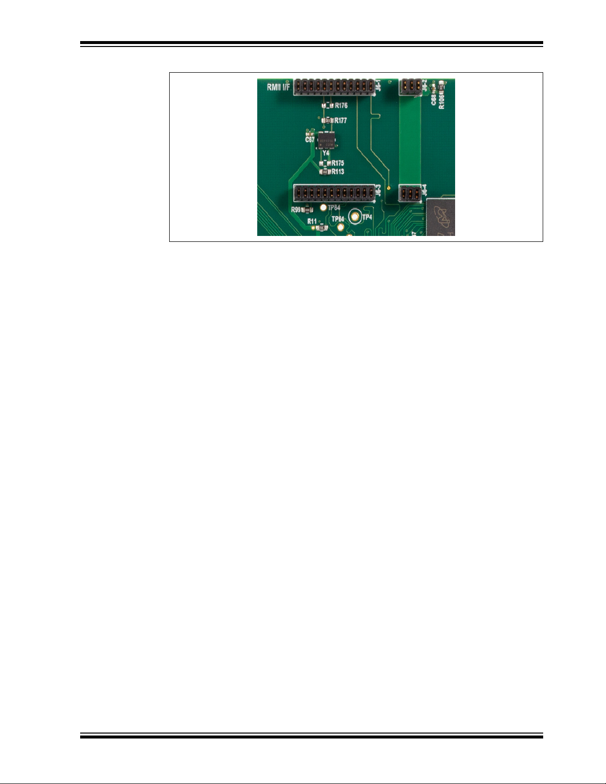
FIGURE 3-4: RMII CONNECTOR
3.8 USB PORTS
The SAMA5D3 EDS board features three USB ports:
• Port A: High-speed and full-speed host multiplexed with
• Port B: High-speed and full-speed host, standard Type A connector J23
• Port C: Full-speed host, standard Type A connector J24
Board Details and Configuration
high-speed USB device,
micro-AB connector J12
3.9 SERIAL UART INTERFACE
Serial I/O communication to the MPU is available on 1x6 pin header J10. Only the RX,
TX, and GND pins are used. The other pins are either not connected or can be ignored.
The default serial port settings are 115200 baud, 8 bits, no parity, and 1 Stop bit (8N1).
This is a 3.3V interface. See Section 4.2.2 “USB-to-Serial Communication Option”
more details on using this connector.
for
3.10 JTAG PORT
A standard 2 x 10-pin JTAG header (J11) is implemented on the board to enable software development and debugging of the boar
interface signals have a voltage level of 3.3V.
3.11 BOARD FEATURES AND SPECIFICATIONS
Figure 3-5 shows the top view of the SAMA5D3 EDS board with its key features, and
Ta bl e 3-2 details the specifications of the SAMA5D3 EDS board.
d using various JTAG emulators. The
2018 Microchip Technology Inc. DS50002789A-page 19
Page 20

SAMA5D3 Ethernet Development System User’s Guide
FIGURE 3-5: SAMA5D3 EDS BOARD’S MAIN FEATURES
TABLE 3-2: SAMA5D3 EDS BOARD SPECIFICATIONS
Characteristics Specifications
Processor SAMA5D36 (324-ball BGA package) ARM® Cortex-A5 Pro-
cessor with v7-A Thumb®-2 instruction set, core frequency
up to 536 MHz
Memory 2 x 1 Gb DDR2 (16M x 16 bits x 8 banks)
1 x 2 Gb NAND flash (256M x 8 bits)
Optional on-board memory One I2C EEPROM
One SPI Serial Flash
SD One 8-bit SD card slot
USB Two USB Hosts
One micro-AB USB device
Ethernet One 1 Gb MAC with RGMII interface
One 10/100 Mb MAC with RMII interface
Debug port One JTAG interface connector
One serial debug interface (3.3V level)
Board supply voltage 12V power jack
User interface Reset push button
LEDs for power, reset, USB, and NAND flash disable
Expansion One 8 x 2 GPIO header with two-wire, SPI, and audio
One 1 x 6 GPIO header with USART
DS50002789A-page 20 2018 Microchip Technology Inc.
Page 21

ETHERNET DEVELOPMENT SYSTEM
Chapter 4. Software Configuration and Operation
4.1 INTRODUCTION
The SAMA5D3 EDS board is pre-configured with Linux and Ethernet drivers. This
includes some command line utilities for controlling certain switch functions. In addition,
the user can interact with the driver to monitor and control the attached switch daughter
board.
This chapter explains how to establish a communication channel from a PC to the
SAMA5D36 MPU and gives some examples of things to do in the bootloader and Linux
environments once connected. Additional documentation on the software capabilities
and usage for this board is available on the Microchip website at
4.2 COMMUNICATION OPTIONS
There are two ways to establish a communication interface from a PC to the MPU:
either via Ethernet or via USB-to-serial.
SAMA5D3
USER’S GUIDE
www.microchip.com.
4.2.1 Ethernet Communication Option – Telnet
1. Connect a compatible Ethernet daughter board to either the RGMII or RMII connector and ensure that all jumper settings are correct on both boards.
2. Connect an Ethernet cable between the daughter board and a PC.
3. Set the network port IP address on the PC to 192.168.0.100 and set the subnet
mask to 255.255.255.0.
4. From a command prompt window on the PC, enter the following command: ping
192.168.0.210
a) If ping doesn't work, there may be a problem with the RGMII/RMII or
SPI/I2C/MDIO interfaces between the boards, with the PC network settings,
or with the IP address on the SMA5D3 EDS board. If the problem cannot be
readily resolved, try the USB-to-Serial option instead.
5. From the same command window on the PC, enter the following command: telnet 192.168.0.210
a) It may be necessary to enable Telnet on a Windows PC by going to Control
Panel > Programs and Features > Turn Windows Features On or Off and
then check the box for Telnet Client.
b) Alternatively, many communication programs such as PuTTY and TeraTerm
can be used to open a Telnet session.
6. The command prompt window should change to Telnet and should display a
login prompt for Linux. The login is “root” (no quotes). No password is required.
See
Figure 4-1.
2018 Microchip Technology Inc. DS50002789A-page 21
Page 22

SAMA5D3 Ethernet Development System User’s Guide
FIGURE 4-1: TELNET LOGIN
7. The Linux file system root is located with command: cd /
4.2.2 USB-to-Serial Communication Option
This option provides direct access to the SAMA5D3 MPU via a UART interface. It does
not require knowledge of the IP address and setting the IP address on the PC. In addition, it does not depend on a switch or PHY
SAMA5D3 EDS board.
1. Get a USB-to-serial cable and install the PC
the Microchip PICkit™ Serial Analyzer, the USB-to-TTL Serial Cable from Adafruit (Product ID 954), and the FTDI TTL-232R-3V3 or TTL-232R-5V.
2. Connect the USB-to-serial cable to header J10 on the SAMA5D3 EDS board.
a) If using the Adafruit USB-to-Serial Cable (Product ID 954), connect white to
pin 2, green to pin 3, and black to pin 6. Red is not used. See Figure 4-2.
J10
daughter board being attached to the
driver if necessary. Examples are
FIGURE 4-2: ADAFRUIT USB-SERIAL CABLE CONNECTION TO HEADER
0
J1
b) If using a TTL-232R cable from FTDI, the 6-pin SIL connector on the cable
plugs directly into J10 on the board, with green at J10 pin 1 and black at J10
pin 6. See Figure 4-3.
DS50002789A-page 22 2018 Microchip Technology Inc.
Page 23

Software Configuration and Operation
FIGURE 4-3: FTDI TTL-232R USB-SERIAL CABLE CONNECTION TO
HEADER J10
3. On the PC, open a serial port session using TeraTerm, PuTTY or similar commu-
nication software. The settings are 115200 baud, 8 bits, no parity, 1 Stop bit
N1).
(8
4. The MPU outputs text as shown in Figure 4-4 when it powers up.
FIGURE 4-4: LINUX LOGIN PROMPT
5. The login is “root” (no quotes). No password is required.
6. The Linux file system root is
4.3 SOFTWARE VERSION
The software installed on the board may not be the latest revision. Users are encouraged to compare the installed software version with the latest version available on the
ochip website and update it if necessary. The software version can be checked as
Micr
follows:
# cat/sys/class/net/eth0/sw/version
located with command: cd /
2018 Microchip Technology Inc. DS50002789A-page 23
Page 24

SAMA5D3 Ethernet Development System User’s Guide
4.4 IP AND MAC ADDRESSES
All SAMA5D3 EDS boards currently come with the same IP and MAC addresses. Use
the ipaddr or ifconfig commands to check the IP and MAC addresses:
# ipaddr or # ifconfig
Either address may be changed at the bootloader level as described in
Section 4.5 “Ethernet Device Register Address”.
4.5 ETHERNET DEVICE REGISTER ADDRESS
When logged into Linux on the board, the registers of the Ethernet switch or PHY on
the attached daughter board can be accessed using the regs_bin utility. The KSZ
Switch Utilities User’s Guide provides more details about regs_bin and other utilities for
certain KSZ switches.
Below is an example of byte, word and double-word reads and writes using regs_bin.
# regs_bin spi0.0
> rb 302 // byte read
0000: 00
> rw 302 // word read
0000: 00 10
> rd 302 // double word read
0302: 00 10 a1 94
> wb 302 87 // byte write
> rd 302
0302: 87 10 a1 94
> ww 304 88 99 // word write
> rd 302
0302: 87 10 88 99
> wd 302 38 47 56 65 // double word write
> rd 302
0302: 38 47 56 65
> q
#
4.6 ETHERNET SWITCH MIB COUNTERS
When a switch daughter board is connected to the SAMA5D3 EDS board, the driver
makes the per-port MIB counters available for reading.
# cat /sys/class/net/eth0/sw0/0_mib // read MIB counters for port 1
# cat /sys/class/net/eth0/sw1/1_mib // read MIB counters for port 2
# cat /sys/class/net/eth0/sw2/2_mib // read MIB counters for port 3
To clear the MIB counters for individual ports:
# echo 0 > /sys/class/net/eth0/sw0/0_mib // clear MIB counters for port 1
# echo 0 > /sys/class/net/eth0/sw1/1_mib // clear MIB counters for port 2
# echo 0 > /sys/class/net/eth0/sw2/2_mib // clear MIB counters for port 3
DS50002789A-page 24 2018 Microchip Technology Inc.
Page 25

Software Configuration and Operation
To clear the MIB counters for all ports at once:
# echo 0 > /sys/class/net/eth0/sw/mib
4.7 BOOTLOADER SETTINGS
Several variables, including device addresses, can be set in the U-Boot bootloader. To
access the boot loader settings, either reboot the processor with the “reboot” command
or press the reset button (SW1) on the board. Then, quickly press any keyboard key
early in the boot process at the message, “Hit any key to stop autoboot,” as shown in
Figure 4.5.
// clear MIB counters for all ports
FIGURE 4-5: U-BOOT EN
Type “print” to see a listing of environment variable settings. Below are examples of
how to set some variables. To make the changes permanent, use the “saveenv” command after making the changes.
=> print
=> setenv ethaddr 00:10:A1:94:77:01
=> setenv ipaddr 192.168.0.201
=> saveenv
=> boot
/ / o p t i o n a l , s ho w t h e e n vironment variable settings
// saves settings to NV memory
TRY POINT
// sets th e M AC address
// sets the I P address
4.8 AUTOMATICALLY RUNNING PROCESS
Depending on the software revision and the attached Ethernet daughter board, some
processes such as AVB or RSTP may be set to run automatically when the system is
powered up. To check if they are running, read the appropriate files in the folder
/sys/class/net/eth0/sw
# cat /sys/class/net/eth0/sw/avb
# cat /sys/class/net/eth0/sw/stp
They can be disabled at the bootloader:
=> setenv avb 0
=> setenv multi_dev 3
=> setenv stp 0 // disable RSTP
=> saveenv /
2018 Microchip Technology Inc. DS50002789A-page 25
// disable AVB
// bug wo rkaround to enable STP control
/ saves settings to NV memory
Page 26

SAMA5D3 Ethernet Development System User’s Guide
4.9 PRECISION TIME PROTOCOL (IEEE 1588)
For switch daughter boards that support IEEE1588 Precision Time Protocol (PTP), the
PTP protocol can be run by navigating to the appropriate file system directory, then run
ning the script found there. There are directories for end-to-end (e2e) and peer-to-peer
(p2P). The default.cfg file found in the e2e and p2p directories can be edited to change
the PTP parameters. Additional details can be found in the software setup guide for the
given switch.
# cd /ptp/e2e
# cd /ptp/p2p
# /linuxptp.sh
4.10 VLAN SETUP
VLAN control of switches is handled through the driver. The user can access the
driver's VLAN functions via files located at /sys/class/net/eth0/sw. Reading
/sys/class/net/eth0/sw/vlan_table shows the valid entries in the VLAN table. See the
appropriate switch reference guide for further details.
4.11 DHCP
-
To enable DHCP, change the word “static” to “dhcp” in the file /etc/network/interfaces.
4.12 NUTTCP TRAFFIC TESTING
The Linux installation includes the nuttcp utility, which has similar capabilities as iperf.
If you install nuttcp on another device such as a PC, you can perform traffic testing
between the two devices. A help menu is included. Additional details about nuttcp can
be found on the Internet.
DS50002789A-page 26 2018 Microchip Technology Inc.
Page 27

SAMA5D3
ETHERNET DEVELOPMENT SYSTEM
USER’S GUIDE
Appendix A. Programming the SAMA5D3 EDS Board
A.1 INTRODUCTION
The software installed on the board may not be the most recent, so users should check the software version
as described in
Microchip website.
A.2 NAND FLASH PROGRAMMING
A.2.1 NAND Flash Programming on Linux
Note: The following procedure is tested with the Ubuntu x64 14.04.05 LTS distribution.
1. Open a terminal window and unzip the file to a folder (for example, /home).
$ unzip SAMA5D3_EDS _Images_Vxx.xx.xx.zip
$ cd SAMA5D3_EDS_Images/linux
2. Connect the micro-USB (J12) connector of the SAMA5D3 EDS board to the Linux PC.
3. Connect 12V of power to the SAMA5D3 EDS board.
4. Remove the NAND enable (J20) jumper and press the reset button.
The /dev/ttyACM0 ____ is created. Execute the $ tail –f /var/log/kernel.log command
to see this.
5. Insert the NAND enable (J20) jumper.
6. If you are using an x86 system, then run the flash_board script in the terminal window. If you are
using an x64 system, then run the flash_board_x64 script.
$ sudo flash_board (for x86 system)
$ sudo flash_board_x64 (for x64 system)
7. Once “DONE” is displayed, press the reset button to reboot the SAMA5D3 EDS board.
Section 4.4 “IP and MAC Addresses” and update it to the latest version available on the
A.2.2 NAND Flash Programming on Windows
Note: This procedure is tested on Win7 x64 and Win10 x64 versions of Windows.
1. Unzip the zip file to a folder (for example, C:\tmp).
2. Open Command Prompt and change the SAMA5D3_EDS_Images\windows folder (for example,
C:\tmp\SAMA5D3_EDS_Images\windows).
3. Connect the micro-USB (J12) connector of the SAMA5D3 EDS board to the Windows PC.
4. Connect 12V of power to the SAMA5D3 EDS board.
5. Remove the NAND enable (J20) jumper and press the reset button.
6. When the PC has Internet connection, it will install “Bossa Program Port” automatically. (The port
number may be different on the system.) See
2018 Microchip Technology Inc. DS50002789A-page 27
Figure A-1.
Page 28

SAMA5D3 Ethernet Development System User’s Guide
FIGURE A-1: DEVICE MANAGER - BOSSA PROGRAM PORT INSTALLED
7. If the PC does not have Internet connection, find “Unknown device” under “Other devices” in Device
Manager and install the driver from the folder. See Figure A-2:
SAMA5D3_EDS_Images\windows\sam-ba_3.1.4\driver
(for example, C:\tmp\SAMA5D
3_EDS_Images\windows\sam-ba_3.1.4\driver)
DS50002789A-page 28 2018 Microchip Technology Inc.
Page 29

Programming the SAMA5D3 EDS Board
FIGURE A-2: DEVICE MANAGER - OTHER DEVICES>UNKNOWN DEVICE
2018 Microchip Technology Inc. DS50002789A-page 29
Page 30

SAMA5D3 Ethernet Development System User’s Guide
8. After successful installation, the Device Manager window shows AT91 USB to Serial Converter
“Ports.” See Figure A-3.
FIGURE A-3: DEVICE MANAGER - AT91 USB TO SERIAL CONVERTER SHOWN
9. Wait for few seconds before performing the following steps after board power-up. Make sure the
device driver installation is complete. Figure A-4 shows the console display after the NAND flash programming is complete.Insert the NAND enable (J20) jumper.
10. Using Command Prompt, execute flash_bo
program the NAND flash.
> cd SAMA5D3_EDS_Images\windows
> flash_board.bat
ard.bat under SAMA5D3_EDS_Images\windows to
DS50002789A-page 30 2018 Microchip Technology Inc.
Page 31

Programming the SAMA5D3 EDS Board
FIGURE A-4: EXECUTING THE FLASH_BOARD.BAT COMMAND IN COMMAND PROMPT
2018 Microchip Technology Inc. DS50002789A-page 31
Page 32

SAMA5D3 Ethernet Development System User’s Guide
If the error in Figure A-5 appears, rerun the flash_board.bat command.
FIGURE A-5: FLASH_BOARD.BAT COMMAND ERROR
A.3 SD CARD IMAGE PROGRAMMING
The SAMA5D3_ESD_Images_Vxx.xx.xx.zip file contains an SD card image that must be flashed to the
SD card. The image is available in the SAMA5D3_ESD_Images/images folder.
To flash images to the SD card, the Etcher tool is
https://etcher.io. The Etcher tool provides the
For Windows, download and install the 32-bit installer
For Linux, download the x86 or x64 package depending on your Linux system. This procedure is tested on
Ubu
ntu x64 14.04.05 LTS distribution.
recommended. The tool can be downloaded from
same GUI interface both for Windows and Linux.
package. This procedure is tested on Win7x64.
A.3.1 SD Card Programming
Note: An SD card size of 16 GB or greater is required.
1. Unzip the zip file to a folder (for example, C:
2. The SD card image (s
(c:\tmp\ SAMA5D3_
3. Start the Etcher tool and select the image (sdcard.img).
selected because all the contents of the SD card will be erased.
4. Select Flas
h! to program the SD card. See Figure A-6.
dcard.img) is located in the SAMA5D3_ESD_Images\images folder.
ESD_Images\images\sdcard.img)folder
\tmp).
Make sure the appropriate SD card is
DS50002789A-page 32 2018 Microchip Technology Inc.
Page 33

Programming the SAMA5D3 EDS Board
FIGURE A-6: ETCHER TOOL
After the programming is successfully completed, the SD card can be used to boot the SAMA5D3 EDS
board.
A.4 BOOTING THE SAMA5D3 EDS
The serial communication interface must be connected to a PC using an FTDI USB-to-Serial
(TTL-232R-3V3) cable. A 12-V power must also be connected to the SAMA5D3 EDS board.
A.4.1 Booting from NAND Flash
The SAMA5D3 EDS board boots with the new image if MCU reset or power on/off is pressed after programming the NAND flash. The “buildroot login:” prompt is di
press <Enter>.
A.4.2 Booting from SD Card
After burning the SD card, insert the SD card into the SD slot. Reset the board either using the reset button
or powering on/off the board. The board boots with the SD card, and “buildroot login:” is prompted. To open
Command Prompt, enter ‘root’ and press <Enter>.
splayed. To open Command Prompt, enter ‘root’ and
2018 Microchip Technology Inc. DS50002789A-page 33
Page 34

SAMA5D3 Ethernet Development System User’s Guide
NOTES:
DS50002789A-page 34 2018 Microchip Technology Inc.
Page 35

ETHERNET DEVELOPMENT SYSTEM
USER’S GUIDE
Appendix B. Schematics
B.1 INTRODUCTION
This appendix includes the SAMA5D3 EDS schematics. See Figure B-1 to Figure B-6.
SAMA5D3
2018 Microchip Technology Inc. DS50002789A-page 35
Page 36

1
1
2
2
3
3
4
4
5
5
6
6
D D
C C
B B
A A
Page Title:
Project Name:
Title Page
SAMA5D3-EnetDevSys (Knave)
PN:
03-10841
Description:
Date:Size: Sheet of Rev
B161
5/16/2018
Designer:
Jennifer Hancock
SAMA5D3 EnetDevSys FDB baseboard
Designed with
Microchip Technology, Inc.
USB/Network Group - UNG
www.Microchip.com
Altium.com
Table of Contents
1
DescriptionSheet
2
3
4
Power - Regulation and MCU
Revision History
A
Revision SummaryRevision Date
Initial release
Author
11/16/2016
6
Title Page & Block Diagram
5
Block Diagram
SoC Main - Flash, SD card, USB
RGMII and RMII, EEPROM, Security. LCD
SoC GPIO
SDRAM
RGMII / MII
12V barrel jack
3V3
2V5
VBUS
1V8
1V2
Regulators
RMII
RGMII I/F Connector (QTS)
RMII I/F Connector
(Curiosity)
3V3
2V5
VDDIOP1 (VARIO)
5V
3V3
12V
MDIO
EEPROM
& MAC ID
Security
USB Port A
Micro AB
Connector
DDR2 RAM
USB
Port C
Typ e A
USB
Port B
Typ e A
SD
Card Slot
JTAG
Header
LCD Connector
GPIO
Headers
SAMA5D36
MCU
USB HS
USB HS
USB HS
Ethernet Switch FDB Base Board with SAMA5D36
NAND Flash
Carl Johnson
B 09/08/2017 Carl JohnsonErrata fixed, 12V added, new minor features
12V
5V
B1 10/02/2017 Carl JohnsonReversed Rt/Rb for 3V3 regulator divider.
C 12/07/2017 Replaced oscillators with crystals for 12MHz and 32.768kHz, revised legend
1 03/20/2018 Released
Jennifer Hancock
MDIO
Kelly Maas05/16/2018 Block diagram corrections, title revision
GMACEMAC
SPI / I2C
SPI
DS50002789A-page 36 2018 Microchip Technology Inc.
SAMA5D3 Ethernet Development System User’s Guide
FIGURE B-1: ETHERNET SWITCH FDB BASE BOARD WITH SAMA5D36
Page 37

SS
EN
SNS
PVIN
SS
FB
EN
SNS
N
V
_1
V
_2
V
3
V
V
5
ADVREF
V
A
V
V
A
V
V
VDDOSC
V
I
V
C
GNDCORE_1
GNDCO
G
_2
G
G
G
_1
G
G
A
_3
G
G
L
G
GNDCORE_4
GNDOSC
G
U
GNDCO
G
_3
GNDCORE_6
G
4
V
_1
V
1
1_1
V
1
1_2
V
VDDBU
VDDCORE_1
VDDCO
V
_3
VDDCORE_4
VDDCO
VDDCORE_6
VDDCO
7
2018 Microchip Technology Inc. DS50002789A-page 37
FIGURE B-2: SAMA5D3 SCHEMATICS - BOARD POWER I/O AND REGULATORS
1
4A FBF1
12V_F
i
Power
MIC45205-1YU3
ANODE
ANODE41BST
PVDD
PVDD
5VDD
5VDD
PWRGD
PVIN ePAD
PVIN
PVIN
PVIN
PVIN
ePAD VOUT
PVIN
PVIN
VIN
EN
FREQ
NC
NC
NC
NC
NC
GND
PGND
PGND
PGND
PGND
PGND
PGND ePAD
RE_2
RE_5
NDIOP
NDIOP
NDIOP_
NDIODDR_4
NDIODDR_3
NDIODDR_1
NDIOM_1
NDB
NDFUSE
NDUTMII
NDPL
NDAN
12V Pwr Off/On
SW2
BST
BST
VOUT
VOUT
VOUT
VOUT
VOUT
VOUT
VOUT
VOUT
VOUT
FB
RIB
RIA
RIA
RIA
SW
SW
SW
SW
SW
SW
SW
ePAD SW
ILIM
VDDCORE_1
VDDCORE_2
VDDCORE_3
VDDCORE_4
VDDCORE_5
VDDCORE_6
VDDCORE_7
VDDIOP10_1
VDDIOP10_2
VDDIOP11_1
VDDIOP11_2
VDDIODDR_1
DDIODDR
VDDIODDR_2
DDIODDR
VDDIODDR_3
DDIODDR_
VDDIODDR_4
DDIODDR_4
VDDIODDR_5
DDIODDR_
VDDUTMIC
MMBD914-7
42
43
44
21
22
23
24
25
26
27
28
29
54
46
39
36
37
38
10
11
12
31
32
33
34
55
51
RE_2
DDCORE
RE_5
RE_
DDIOP10
DDIOP10_2
DDIOP
DDIOP
VDDIOM_1
DDIOM_1
VDDIOM_2
DDIOM_2
VDDBU
VDDFUSE
DDFUSE
VDDOSC
VDDUTMII
DDUTMI
VDDPLLA
DDPLL
VDDANA
DDAN
DDUTMI
ADVREF
31
2
Power
5VSW
Power
R36
0R
12V_EXT
5VFQ
i
R8
20k
R28
10k
TP34
C39
0.1uF
1
Power
i Power
A16
N13
V17
H14
4A
i
40
4
5
2
3
47
53
14
15
16
17
18
19
49
48
50
9
13
5VEN
20
30
35
1
6
7
8
45
52
56
U7H
GNDCORE_1
C9
GNDCORE_2
GNDCORE_3
GNDCORE
T8
GNDCORE_4
T14
GNDCORE_5
GNDCORE_6
J7
GNDIOP_1
N11
GNDIOP_2
GNDIOP_2
U7
GNDIOP_3
E5
GNDIOP_4
GNDIODDR_5
GNDIODDR_5
F15
GNDIODDR_4
F13
GNDIODDR_3
F10
GNDIODDR_2
GNDIODDR
E14
GNDIODDR_1
J11
GNDIOM_1
T17
GNDIOM_2
GNDIOM_2
T13
GNDBU
P4
GNDFUSE
T11
GNDOSC
R12
GNDUTMII
P10
GNDPLL
L4
GNDANA
ATSAMA5D36A-CU
J1
12V (typ)
1
2.5 mm
2
3
BARREL JACK
A A
R1
5VPG 0R
12V_SW
C32
C33
25V
50V
10uF
0.1uF
R143
B B
C C
D D
100k
R148
510k
A copper plane for
GNDUTMI covers all
USB components
GNDUTMI
2
R9
1k
D9
C27
0.1uF
i
C36
C34
C35
0.1uF
47uF
47uF
C25
C26
DNP
DNP
47uF
47uF
R26
0R
R145
0R
DNP
R149
1.37k
1%
C5
15pF
1V2
C5
C7
D14
T7
T15
U17
V7
G7
V11
VDDIOP1
L11
M4
1V8
D13
F14
G10
G13
H11
VDDIOM
P12
T16
3V3
V15
R3
VDDOSC
U11
U13
VDDPLLA
R10
VDDANA
L6
VDDUTMIC
V13
C116
L5
0.1uF
GNDUTMI
2
12V_SW
R17
22R
C37
0.1uF
C30
DNP
120uF
VDDIOP0
TP60
TP59
VDDOSC
5VFB
1V2
1V8
12V / 2A - 4A
On-board current < 2A
i Power
TP6
C38
R22
0.1uF
DNP
2.2k
R23
10k
1%
R144
1.91k
1%
C88
C89
0.1uF
0.1uF
C98
C99
0.1uF
0.1uF
C103
C102
0.1uF
0.1uF
2V5
R86
100R
VDDPLLA VDDANA
C111
C114
0.1uF
0.1uF
C4
2200pF
"5V Ext."
D3
GREEN
C90
0.1uF
VDDIOP1
C97
0.1uF
C104
0.1uF
Power
VDDIOM
C115
0.1uF
i
C91
0.1uF
C100
0.1uF
TP12
C108
0.1uF
3
5V / 6A
On-board current < 2A
Switching Frequency = ~500kHz
C92
C93
0.1uF
0.1uF
3V3
C109
C110
0.1uF
0.1uF
3
C95
1uF
C113
0.1uF
4
3V3 / 3A
R161
10R
C61
1uF
R10
3V3PG
1V2 PG
DNP
R29
10R
C49
1uF
On-board current < 2A
10k
U6
11
PVIN
PVI
PVIN10SW
9
AVIN
4
EN
3
PG
7
SS
8
AGND
13
C63
ePAD
MIC23303YML/ADJ
0.1uF
10k
11
9
4
TP1
3
7
8
13
C48
0.1uF
1V8
2V5_EXT
3V3
1.2V / 3A
On-board current < 1.6A
U5
PVIN
PVIN10SW
AVIN
EN
PG
SS
AGND
ePAD
MIC23303YML
5V
C53
4.7uF
5V
3V3
FB7
220R
FB5
220R
R33
3V3_R
2.2R
i
Power
FB11
220R
1V2
R34
1V2_R1
2.2R
Power
R35
1V2_R3
2.2R
Power
5VPG
5V
C23
4.7uF
TP87
Power
i
Power
i
L3
10uH
Power
Power
i
L4
10uH
i
Power
L5
10uH
i
Power
VDDIOP0
VDDIOM
VDDOSC
i
VDDANA
VDDPLLA
i
VDDUTMIC
i
C87
4.7uF
C107
4.7uF
C112
4.7uF
DNP
FB2
4
R159
C54
R160
10k
0.1uF
DNP
C60
C59
10000pF
0.1uF
C2
R4
10k
0.1uF
DNP
3V3PG
C47
C46
10000pF
0.1uF
VDDIOP1
220R
J2
1 2
3 4
5 6
Install only one jumper to select one
voltage at a time. Voltage LED circuit
is shown on page 6.
SAMA5D36 Power Distribution
SAMA5D36 Power Sequencing Requirements
Power up:
All 1V2 rails should come up at least 1ms after the other power rails.
Reset should be release after 1V2 comes up.
Power down:
Voltage rails can be removed in any sequence.
PGND
5
TP21
FB3
3v3_L
220R
TP86
C57
C58
10uF
10uF
TP88
TP17
i
FB1
1v2_L
220R
C43
C44
C45
10uF
10uF
10uF
TP26
2.5V / 1A
On-board current < 0.4A
U2
VIN2VOUT
1
10k
SHDN
3
GND
6
GND (TAB)
MCP1826T-ADJ
1.8V / 1A
On-board current < 0.2A
U4
VIN2VOUT
10k
1
SHDN
3
GND
6
GND (TAB)
MCP1826T-ADJ
Designer:
3V3
1V2
TP19
Jennifer Hancock
Power
i
1
SW
2
5
SNS
6
FB
12
Power
1
SW
2
5
SNS
6
FB
12
PGND
5
Power
i
L1
470nH
3v3out
R162
C55
464k
33pF
C56
10uF
R163
107k
i
Power
L2
470nH
1v2out
C42
R31
240k
33pF
1%
R32
249k
1%
3V3
R18
C28
4.7uF
3V3
R24
C7
4.7uF
Description:
SAMA5D3 EnetDevSys FDB baseboard
Page Title:
Board Power I/O and Regulators
Project Name:
SAMA5D3-EnetDevSys (Knave)
B261
Date:Size: Sheet of Rev
3/22/2018
6
i Power
R21
1k
D2
Grn
i Power
Power
i
4
5
ADJ
Power
i
4
5
ADJ
Microchip Technology, Inc.
USB/Network Group - UNG
www.Microchip.com
PN:
6
3V3
R19
102k
R20
20k
R25
68k
R27
20k
03-10841
2V5
1V8
"3V3"
C29
4.7uF
C22
4.7uF
TP23
TP25
TP22
TP24
Designed with
Altium.com
Schematics
Page 38

0
1
2
5
6
7
VCC
GND
VBUS
G
D+
VBUS
G
VCC
GNDGG
DS50002789A-page 38 2018 Microchip Technology Inc.
SAMA5D3 Ethernet Development System User’s Guide
FIGURE B-3: SAMA5D3 SCHEMATICS - SOC CORE CONNECTIONS, NAND FLASH, AND SD CARD
1
VDDIOP0
C20
0.1uF
5
R6
1k
RST_B
VDDIOP0
NANDRDY
C6
0.1uF
D10
D11
D12
D13
D14
D15
U16
74LVC1G14GW,125
VCC
24
GND
3
Reset (200ms delay)
VDDIOP0
U10
6
5
7
MIC826TYMT
R154
0R
DNP
R155
0R
DNP
R156
0R
K12
D0
K15
D1
K14
D2
K16
D3
K13
D4
K17
D5
J12
D6
K18
D7
J14
D8
J16
D9
J13
J17
J15
J18
H16
H18
L12
L17
K11
L18
1
RESET
VCC
MR
GND2RESET
ePAD
R153
0R
Y1
12MHz
1 3
R158
0R
Y2
32.768kHz
Match Lengths
NANDCE_J
NRD
NWE
NANDRDY
WDI
i
FLASH_D0
FLASH_D
FLASH_D1
FLASH_D
FLASH_D2
FLASH_D
FLASH_D3
FLASH_D3
FLASH_D4
FLASH_D4
FLASH_D5
FLASH_D
FLASH_D6
FLASH_D
FLASH_D7
FLASH_D
3
4
1
XOUT_12M
12_Mhz
32.768kHz
NAND Enable
J20
1
2
15pF
15pF
15pF
15pF
VDDIOP0
R119
10k
DNP
NRST 4
"Reset"
D5
RED
A A
SW1
1 4
2 3
Reset
B B
XOUT_32K
C C
NAND FLASH
PE22_CLE6
PE21_ALE6
U7G
D D
NCS3_NANDCS
NRD_NANDOE
NWE_NANDWE
ATSAMA5D36A-CU
2
C41
C50
C51
C52
VDDIOP1
VDDIOM
12_Mhz
XOUT_12M
32.768kHz
XOUT_32K
TP52
R72
100k
TP33
TDI
TMS
TCK
TDO
NTRST
NRST
R75
R76
PE3_PRTPWRB6
PE5_OCS6
PE4_PRTPWRC6
R90
1k
NRD
NANDCE
NWE
2
U8
V8
U16
V16
T10
T12
T9
R8
N10
P9
M11
P11
V9
U15
10k
U9
10k
ATSAMA5D36A-CU
5V
C16
47uF
C19
47uF
74LVC1G14GW,125
U11
29
I/O0
30
I/O1
31
R/B
I/O2
32
I/O3
41
I/O4
DNU
42
I/O5
DNU
43
I/O6
44
VCC
I/O7
VCC
8
RE
VCC
9
CE
VCC
16
VSS
CLE
17
VSS
ALE
18
WE
VSS
19
WP
VSS
MT29F2G08ABAEAWP
2Gbx8b, NAND Flash
R91
10k
U7I
XIN
XOUT
XIN32
XOUT32
WKUP
SHDN
JTAGSEL
TDI
TMS_SWDIO
TCK_SWCLK
TDO
NTRST
NRST
TST
BMS
U14
6
4
3
MIC2009YML
U15
6
4
3
MIC2009YML
C8
7
38
47
12
34
37
39
13
25
36
48
VIN
EN
FAULTn
VIN
EN
FAULTn
0.1uF
2 4
HHSDMA
HHSDPA
HHSDMB
HHSDPB
HHSDMC
HHSDPC
DIBN
ILIMIT
ILIMIT
3V3
5
VCC
GND
3
C164
0.1uF
DIBP
VBG
VOUT
ePAD
VOUT
ePAD
3
V10
U10
V12
U12
V14
U14
U6
V6
R11
R74
5.62k
1%
GNDUTMI
VBUSB
1
2
5
R97
GND
7
124R
1%
1
VBUSC
2
5
R101
GND
7
124R
1%
"NAND Act."
U12
D1
VDDIOM
R89
C165
10k
0.1uF
3
USBA_D_N
USBA_D_P
USBB_D_N
USBB_D_P
USBC_D_N
USBC_D_P
TP53
TP62
VBG
RED
C15
47uF
Power
C18
47uF
C161
10pF
Power
D8
R150
C13
2.2k
GREEN
"Vbus"
i
R110
1k
DNP
i
R111
1k
DNP
R7
1k
2.2uF
R109
2.2k
R112
2.2k
VBUS
4
R70
20k
i Power
1
2
3
4
5
EARTH_USB
1
2
3
4
EARTH_USB
D6
GREEN
1
2
3
4
EARTH_USB
D7
GREEN
R71
40.2k
J12
VBUS
DD+
USBA (UFP)
ID
MICRO_USB-AB
GND
C3
0.1uF
0
R3
330R
J23
VBUS
USBB (MCU EHCI Cntl.)
D-
USB2.0 STD-A FEMALE
D+
GND
ND
C14
0.1uF
0
R96
330R
"Port B"
J24
VBUS
USBC (MCU EHCI Cntl.)
D-
USB2.0 STD-A FEMALE
D+
GND
ND
C17
0.1uF
0
R98
330R
"Port C"
4
PE9_VBUS_DET 6
SD CARD
PE0_MCI0_CD6
PD0_MCI0_CDA6
PD1_MCI0_DA06
PD2_MCI0_DA16
PD3_MCI0_DA26
PD4_MCI0_DA36
PD9_MCI0_CK6
PD5_MCI0_DA46
PD6_MCI0_DA56
PD7_MCI0_DA66
PD8_MCI0_DA76
VDDIOP1
68k
R77
5
Serial UART
PE136
PB31_TXD4
PB30_RXD4
PE146
DNP
R65
0R
DNP
R67
0R
VDDIOP0
R59
68k
6
R60
68k
J10
1
2
"2 TXD"
3
"3 RXD"
4
5
6
"6 GND"
MCU is not using pins 1 and 5 of this port
JTAG
NTRST
TDI
TMS
TCK
TDO
NRST
VDDIOM
R78
R79
R80
R81
R82
R83
R84
R85
J14
2
CMD
7
D0
8
D1
9
D2
1
D3
5
CLK
10
D4
11
D5
12
D6
13
SWGND1
D7
SWGND2
20
SWGND3
NC
21
SWGND4
NC
Proconn Technology
SD/MMC Card Connector
Description:
Page Title:
Project Name:
B361
Date:Size: Sheet of Rev
5
VDDIOP0
R61
R62
100k
0R
VDD_MDCI0
C162
10uF
R120
330R
Designer:
100k
Q1
312
IRLML6402
C163
0.1uF
C169
0.1uF
Jennifer Hancock
R66
R87
10k
4
VDD
3
GND
6
GND
14
CD
15
WP
16
17
18
19
SAMA5D3 EnetDevSys FDB baseboard
SoC core connections, NAND Flash, SD Card
SAMA5D3-EnetDevSys (Knave)
5/17/2018
3V3
R64
R63
100k
100k
R68
0R
R69
0R
HDR-2.54 Male 2x10
VDDIOP1
R73
100k
PE2_PWR_MCI0 6
Microchip Technology, Inc.
USB/Network Group - UNG
www.Microchip.com
PN:
03-10841
6
J11
1 2
3 4
5 6
7 8
9 10
11 12
13 14
15 16
17 18
19 20
Designed with
Altium.com
Page 39

1
1
2
2
3
3
4
4
5
5
6
6
D D
C C
B B
A A
Page Title:
Project Name:
RGMII and RMII I/F Connectors
SAMA5D3-EnetDevSys (Knave)
PN:
03-10841
Description:
Date:Size: Sheet of Rev
B461
5/16/2018
Designer:
Jennifer Hancock
SAMA5D3 EnetDevSys FDB baseboard
Designed with
Microchip Technology, Inc.
USB/Network Group - UNG
www.Microchip.com
Altium.com
i
Net Class
ClassName: RGMII_RX
i
Net Class
ClassName: RGMII_RX
i
Net Class
ClassName: RGMII_TX
GMII layout requirements
1. Match lengths within 20 mils within
the RGMII_RX and RGMII_TX classes.
2. RX signals do not need to be
length-matched to TX signals.
PB30_RXD 3
PB31_TXD 3
GTXD0
GRXD0
GRXD1
GRXD2
GRXD3
GTXC
GTXEN
GRXCK
GRXDV
VDDIOP1
10k
R92
22R
R93
CTXER
0.1uF
C170
TP8
GTXD_R0
GTXD1GTXD_R1
GTXD2GTXD_R2
GTXD3GTXD_R3
TP9 TP10 TP11
ETX0ETX_R0
PC14_LCDDAT16
PC13_LCDDAT17
PC12_LCDDAT18
PC11_LCDDAT19
PC10_LCDDAT20
PC15_LCDDAT21
PC22_SPI1_MISO 4, 6
PC23_SPI1_MOSI 4, 6
PC24_SPI1_SPCK 4, 6
PC25_SPI1_NPCS0 6
PC26_TWD1
PC27_TWCK1
3.3k
R132
3.3k
R133
VDDIOP0
ETX_R1
ERX0
ERX1
ETXEN
ECRSDV
ERXER
EREFCK
EMDC
EMDIO
PA0_LCDDAT0
PA1_LCDDAT1
PA2_LCDDAT2
PA3_LCDDAT3
PA4_LCDDAT4
PA5_LCDDAT5
PA6_LCDDAT6
PA7_LCDDAT7
PA8_LCDDAT8
PA9_LCDDAT9
PA10_LCDDAT10
PA11_LCDDAT11
PA12_LCDDAT12
PA13_LCDDAT13
PA14_LCDDAT14
PA15_LCDDAT15
PC14_LCDDAT16
PC13_LCDDAT17
PC12_LCDDAT18
PC11_LCDDAT19
PC10_LCDDAT20
PC15_LCDDAT21
PA28_LCDPCK
PA26_LCDVSYNC
PA27_LCDHSYNC
PA29_LCDDEN
PA25_LCDDISP
PA24_LCDPWM
NRST3, 4
0R
R48
5V3V3
0R
R47
PC26_TWD1
PC27_TWCK1
PE6_RST_LCD6
PE8_IRQ26
PE7_IRQ16
TP29 TP30 TP31 TP32
5V
PA28_R
iPower
PD20_AD06
PD21_AD16
PD22_AD26
PD23_AD36
PC26_R
PC27_R
GMDIO
GMDC
PE23_ID_SYS6
PE27_LCDDAT226
PE28_LCDDAT236
GTXD0
GTXD1
GTXD2
GTXD3
GTXEN
GRXCK
GRXD0
GRXD1
GRXD2
GRXD3
PC16_TK0_AUDIO 6
PC17_TF0_AUDIO 6
PC18_TD0_AUDIO 6
PC19_RK0_AUDIO 6
PC20_RF0_AUDIO 6
PC21_RD0_AUDIO 6
i
Net Class
ClassName: MII_TX
i Net Class
ClassName: MII_RX
2V5_EXT 3V3
4.7uFC94.7uF
C10
4.7uF
C11
(AVB)
<PME_N)
(1588)
(DUPLEX>
RMII layout requirements
1. Match lengths within 50 mils
within the MII_RX and MII_TX
classes.
2. Match RX signals to TX
signals +/- 500 mil.
2V5_EXT
2V5
i
Power
10uF
C62
(IRQ_N>
0
N
0
V
VDDIOP0
0.1uF
C167
<RST_DCARD)
GCRS
GCOL
GTXD4
GTXD5
GTXD6
GTXD7
GRXD5
GRXD6
GRXD7
GRXD4
<25MHZ_REFCLK)
GRXDV
GTXD4
GTXD5
GTXD6
GTXD7
GRXD5
GRXD6
GRXD7
GRXD4
CLK125_R
3V3_RGMII2V5_RGMII
5V_RGMII
VDDIOP1
3V3_RGMII
2V5_RGMII
5V_RGMII
V
1
3V3_RGMII
2V5_RGMII
5V_RGMII
i
Power
VDDIOP1
CLK125
5V up to 2.5A
3.3V 1.5A
2.5V 0.6A
1.8V 0.8A
Available power to the
RGMII connector:
PC24_SPI1_SPCK
PC23_SPI1_MOSI
PC22_SPI1_MISO
<COL)
IRQ_N
<SPICS)
(SPIMOSI)
(SPIMISO)
<SPICK)
<GMDC/SPICK)
(MDIO/SPIMOSI)
G125CK
GCOL
<CRS)GCRS
<RXER)
(TXER>
<TXCLK)
(TXC>
(TXCTL/EN>
(TXD0>
(TXD1>
(TXD2>
(TXD3>
(TXD4>
(TXD5>
(TXD6>
(TXD7>
<RXD0)
<RXD1)
<RXD2)
<RXD3)
<RXD4)
<RXD5)
<RXD6)
<RXD7)
<RXCTL)
<RXCK)
(CLK125>
(VARIO)
(2V5)
(3V3)
(5V-12V)
(VARIO)
(2V5)
(3V3)
(5V)
VDDIOP1
10k
R94
CTXER
GRXER
GRXER
GRXCTL
GTXCK_R
GTXEN_R
<RXDV)
VDDIOP1
10k
DNP
R15
IRQ_N
MDC/CK/SCL
MDIO/MOSI/SDA
25REFCLK25CLK_R
25REFCLK
VDDIOP1
10k
R118
DUPLEX
A
1
B
2
GND
3
Y
4
VCC
5
A
GND
VCC
74AHC1G08SE-7
U17
VDDIOP1
0.1uF
C1
NRST 3, 4
RST_PHY_N
RST_DCARD_N
GTXC
G125_R
VDD_LCD
NC
1
NC
2
NC
3
GND
4
SDA
5
SCL
6
NC
7
VCC
8
NC
NC
NC
GNDSDA
SC
NC
VCC
EP
9
ATECC508AU19
PA18_TWD2
PA19_TWCK2
VDDIOP0
VDDIOP0
0.1uF
C21
PA18_TWD2
PA19_TWCK2
47k
R141
47k
R142
Clk125
EEPROM Enable
Sec. Dev. Enable
RGMII/MII Connector I/F (GMAC)
RMII Connector I/F
LCD Connector
Security
MAC ID & EEPROM
CLK125
Device/switch pull-downs must overcome the internal
pull-ups in the SAMA5D36. 10K is effective.
ETXEN_R
GTXCCLK125O
PME_N
<SCL)
(SDA)
33R
R117
33R
DNP
R126
33R
R134
33R
R135
33R
R136
33R
R137
33R
R138
33R
R140
33R
R5
33R
R13
33R
R124
33R
R125
33R
R51
33R
R53
33R
R55
33R
R57
33R
R58
PD12_SPI0_SPCK 4, 6
PD11_SPI0_MOSI 4, 6
PD10_SPI0_MISO 6
PD13_SPI0_NPCS0 6
PC22_SPI1_MISO4, 6
PC23_SPI1_MOSI4, 6
PC24_SPI1_SPCK4, 6
PC28_SPI1_NPCS34, 6
PME_N 6
DUPLEX 6
RST_PHY_N 6
10k
DNP
R157
TP63
TP64
TP84
12V_SW
12V_RGMII
10uF
C12
i
Power
10uF
25V
C64
1
2
MMCX, Vert
DNP
J31
DNP
TP5
DNPTP70
DNPTP51
DNPTP50
DNPTP49
DNPTP48
DNPTP46
DNPTP45
DNPTP44
DNPTP43
DNPTP42
DNPTP41
DNPTP40
DNP
TP36
DNP
TP35
12
J3
12
J17
12
J13
12
J7
1
2
J28
1
2
J29
STB
1
GND
2
OUT
3
VDD
4
DSC1001/125MHz
Y3
0R
DNP
R46
0R DNP
R49
0R DNP
R50
0R DNP
R52
0R DNP
R54
0R DNP
R56
A0
1
SDA
5
A2
3
A1
2
WP
7
VSS
4
SCL
6
VCC
8
24AA256
DNP
U1
Place at Refdes: U1
1
3
5
7
9
11
13
15
17
19
21
23
25
27
29
31
33
35
37
39
41
43
45
47
49
2
0
4
6
8
10
12
14
16
18
20
22
24
26
28
30
32
34
36
38
40
42
44
46
48
50
FFC/FPC 50P Female
DNP
J9
PB0_GTX0
T2
PB1_GTX1
N7
PB2_GTX2
T3
PB3_GTX3
N6
PB4_GRX0
P5
PB5_GRX1
T4
PB6_GRX2
R4
PB7_GRX3
U1
PB8_GTXCK
R5
PB9_GTXEN
P3
PB10_GTXER
R6
PB11_GRXCK
V3
PB12_GRXDV
P6
PB13_GRXER
V1
PB14_GCRS
R7
PB15_GCOL
U3
PB16_GMDC
P7
PB17_GMDIO
V2
PB18_G125CK
V5
PB19_GTX4
T6
PB20_GTX5
N8
PB21_GTX6
U4
PB22_GTX7
M7
PB23_GRX4
U5
PB24_GRX5
M8
PB25_GRX6
T5
PB26_GRX7
N9
PB27
V4
PB28
M9
PB29
P8
PB30
M10
PB31
R9
ATSAMA5D36A-CU
U7B
PC0_ETX0
D8
PC1_ETX1
A4
PC2_ERX0
E8
PC3_ERX1
A3
PC4_ETXEN
A2
PC5_ECRSDV
F8
PC6_ERXER
B3
PC7_EREFCK
G8
PC8_EMDC
B4
PC9_EMDIO
F7
PC10
A1
PC11
D7
PC12
C6
PC13
E7
PC14
B2
PC15
F6
PC16
B1
PC17
E6
PC18
C3
PC19
D6
PC20
C4
PC21
D5
PC22
C2
PC23
G9
PC24
C1
PC25
H10
PC26
H9
PC27
D4
PC28
H8
PC29
G5
PC30
D3
PC31
E4
ATSAMA5D36A-CU
U7C
0R DNP
R30
0R
DNP
R95
1
3
5
7
9
11
13
15
17
19
2
4
6
8
10
12
14
16
18
20
21
23
25
27
29
31
33
35
37
39
41
43
45
47
49
51
53
55
57
59
61
63
65
67
69
71
73
75
77
79
81
83
85
87
89
91
93
95
97
99
22
24
26
28
30
32
34
36
38
40
42
44
46
48
50
52
54
56
58
60
62
64
66
68
70
72
74
76
78
80
82
84
86
88
90
92
94
96
98
100
0
GND
101-108
QSS-050-XX-L-D-A-GP
J5
33R
R16
ETX1
A 08-LC-TT
SKT1
ECRSDV
ERX1
ERX0
ERXER
EMDC
EMDIO
ETXEN
ETX0
ETX1
EREFCK
VDDIOP0
10k
R11
10k
DNP
R12
VDDIOP0
Black
DNP
TP4
PA0_LCDDAT0
PA1_LCDDAT1
PA2_LCDDAT2
PA3_LCDDAT3
PA4_LCDDAT4
PA5_LCDDAT5
PA6_LCDDAT6
PA7_LCDDAT7
PA8_LCDDAT8
PA9_LCDDAT9
PA10_LCDDAT10
PA11_LCDDAT11
PA12_LCDDAT12
PA13_LCDDAT13
PA14_LCDDAT14
PA15_LCDDAT15
PA26_LCDVSYNC
PA27_LCDHSYNC
PA29_LCDDEN
PA25_LCDDISP
PA24_LCDPWM
PA28_LCDPCK
3.3k
R127
3.3k
R128
VDDIOP0
PA18_R
PA19_R
PA31_TWCK0_UTXD1 6
PA30_TWD0_URXD1 6
PA18_TWD2
PA19_TWCK2
TP37
TP47
TP54
TP55
TP56
TP57
33R
R129
33R
R130
PA0_LCDDAT0
E3
PA1_LCDDAT1
F5
PA2_LCDDAT2
D2
PA3_LCDDAT3
F4
PA4_LCDDAT4
D1
PA5_LCDDAT5
J10
PA6_LCDDAT6
G4
PA7_LCDDAT7
J9
PA8_LCDDAT8
F3
PA9_LCDDAT9
J8
PA10_LCDDAT10
E2
PA11_LCDDAT11
K8
PA12_LCDDAT12
F2
PA13_LCDDAT13
G6
PA14_LCDDAT14
E1
PA15_LCDDAT15
H5
PA16_LCDDAT16
H3
PA17_LCDDAT17
H6
PA18_LCDDAT18
H4
PA19_LCDDAT19
H7
PA20_LCDDAT20
H2
PA21_LCDDAT21
J6
PA22_LCDDAT22
G2
PA23_LCDDAT23
J5
PA24_LCDPWM
F1
PA25_LCDDISP
J4
PA26_LCDVSYNC
G3
PA27_LCDHSYNC
J3
PA28_LCDPCK
G1
PA29_LCDDEN
K4
PA30_TWD0
H1
PA31_TWCK0
K3
ATSAMA5D36A-CU
U7A
MDC/CK/SCL PA19_TWCK2
PD11_SPI0_MOSI 4, 6
PA18_TWD2
25RefClk
1
2
RF MMCX Female, Vert
DNP
J27
DNP
TP2
Black
DNP
TP3
PA19_TWCK2
PA18_TWD2
GMDC
0.1uF
C31
VDDIOP1
VDDIOP1
VDDIOP1
VDDIOP1
0.1uF
C40
0.1uF
C65
SEL1 6
SEL2 6
NRST3, 4
0R
R99
1B0
5
GND
6
1B121A
3
VCC
1
S1
4
2B0
7
2B1102A
9
S2
8
FSA2259
U20
1B0
5
GND
6
1B121A
3
VCC
1
S1
4
2B0
7
2B1102A
9
S2
8
FSA2259
U21
1B0
5
GND
6
1B121A
3
VCC
1
S1
4
2B0
7
2B1102A
9
S2
8
FSA2259
U22
IRQ_N
EREFCK
1
2
3
J6-4
1
2
3
4
5
6
7
8
9
10
11
12
J6-3
1
2
3
4
5
6
7
8
9
10
11
12
J6-1
PD12_SPI0_SPCK 4, 6
SEL3 6
GMDIO
MDIO/MOSI/SDA
MII
330R
R106
0.1uF
C68
1
2
3
J6-2
i Power
PC28_SPI1_NPCS3
PC28_SPI1_NPCS3
PC24_SPI1_SPCK
PC23_SPI1_MOSI
PC22_SPI1_MISO
PC28_SPI1_NPCS3 4, 6
VDDIOP0
10k
R113
0.1uF
C67
50MHz_OUT
10k
DNP
R175
STB
1
GND
2
OUT
3
VDD
4
DSC1001/50MHz
Y4
3V3
0R
DNP
R176
EREFCK_R
33R
R177
PD14_GPIO 6
PD15_GPIO 6
PD16_GPIO 6
0R
R14
220R
FB6
(EMAC)
2018 Microchip Technology Inc. DS50002789A-page 39
FIGURE B-4: SAMA5D3 SCHEMATICS - RGMII AND RMII I/F CONNECTORS
ERX
ERX
ECRSD
EREFCK
ETX
ETXE
DDIOP
L
Schematics
Page 40

1
1
2
2
3
3
4
4
5
5
6
6
D D
C C
B B
A A
Page Title:
Project Name:
DDR2 SDRAM
SAMA5D3-EnetDevSys (Knave)
PN:
03-10841
Description:
Date:Size: Sheet of Rev
B561
3/21/2018
Designer:
Jennifer Hancock
SAMA5D3 EnetDevSys FDB baseboard
Designed with
Microchip Technology, Inc.
USB/Network Group - UNG
www.Microchip.com
Altium.com
DDR_A0
DDR_A1
DDR_A2
DDR_A3
DDR_A4
DDR_A5
DDR_A6
DDR_A7
DDR_A8
DDR_A9
DDR_A10
DDR_A11
DDR_A12
DDR_A13
DDR_A[0..13]
DDR_D[0..15]
DDR_D0
DDR_D1
DDR_D2
DDR_D3
DDR_D4
DDR_D5
DDR_D6
DDR_D7
DDR_D8
DDR_D9
DDR_D10
DDR_D11
DDR_D12
DDR_D13
DDR_D14
DDR_D15
DDR_D[16..31]
DDR_D16
DDR_D17
DDR_D18
DDR_D19
DDR_D20
DDR_D21
DDR_D22
DDR_D23
DDR_D24
DDR_D25
DDR_D26
DDR_D27
DDR_D28
DDR_D29
DDR_D30
DDR_D31
DDR_A0
DDR_A1
DDR_A2
DDR_A3
DDR_A4
DDR_A5
DDR_A6
DDR_A7
DDR_A8
DDR_A9
DDR_A10
DDR_A11
DDR_A12
DDR_A13
DDR_A[0..13]
DDR_A0
DDR_A1
DDR_A2
DDR_A3
DDR_A4
DDR_A5
DDR_A6
DDR_A7
DDR_A8
DDR_A9
DDR_A10
DDR_A11
DDR_A12
DDR_A13
DDR_A[0..13]
DDR_D0
DDR_D1
DDR_D2
DDR_D3
DDR_D4
DDR_D5
DDR_D6
DDR_D7
DDR_D8
DDR_D9
DDR_D10
DDR_D11
DDR_D12
DDR_D13
DDR_D14
DDR_D15
DDR_D[0..15]
DDR_D16
DDR_D17
DDR_D18
DDR_D19
DDR_D20
DDR_D21
DDR_D22
DDR_D23
DDR_D24
DDR_D25
DDR_D26
DDR_D27
DDR_D28
DDR_D29
DDR_D30
DDR_D31
DDR_D[16..31]
DDR_BA0
DDR_BA1
DDR_BA2
DDR_RAS
DDR_CAS
DDR_CKE
DDR_CLK_P
DDR_CLK_N
DDR_CS
DDR_WE
DDR_DQM0
DDR_DQM1
DDR_DQM2
DDR_DQM3
DDR_DQS0
DDR_DQS1
DDR_DQS2
DDR_DQS3
DDR_VREF
200R
1%
R45
0.1uF
C152
200R 1%
R43
1V8
1V8
10uH
L6
0.1uF
C156
0.1uF
C153
1R
R41
DDR_VREF
DDR_BA0
DDR_BA1
DDR_BA2
DDR_CKE
DDR_CLK_P
DDR_CLK_N
DDR_CS
DDR_RAS
DDR_CAS
DDR_WE
DDR_DQS1
DDR_DQS0
DDR_DQM0
DDR_DQM1
DDR_DQM2
DDR_DQM3
DDR_DQS3
DDR_DQS2
4.7k
R37
4.7k
R39
DDR_BA0
DDR_BA1
DDR_BA2
DDR_CKE
DDR_CLK_P
DDR_CLK_N
DDR_CS
DDR_RAS
DDR_CAS
DDR_WE
4.7k
R38
4.7k
R40
0.1uF
C119
0.1uF
C121
0.1uF
C123
0.1uF
C125
0.1uF
C127
0.1uF
C129
0.1uF
C131
0.1uF
C133
0.1uF
C135
0.1uF
C137
0.1uF
C139
0.1uF
C141
0.1uF
C143
0.1uF
C145
0.1uF
C147
0.1uF
C149
0.1uF
C151
1V8
0.1uF
C118
0.1uF
C120
0.1uF
C122
0.1uF
C124
0.1uF
C126
0.1uF
C128
0.1uF
C130
0.1uF
C132
0.1uF
C134
0.1uF
C136
0.1uF
C138
0.1uF
C140
0.1uF
C142
0.1uF
C144
0.1uF
C146
0.1uF
C148
1V8
0.1uF
C150
DDR_VREF DDR_VREF
DDR2 SDRAM
Keep DDR2 nets as short as possible.
Therefore, place the DDR2 devices as close as possible to the SAMA5D3.
Control the trace impedance of the DDR2 lines to Z0= 50ohm.
Address, control and data group traces may not exceed 1.3 inches (33mm).
Match trace lengths within the address, control and data groups to within 0.1 inch (2.54mm).
Match address and control group trace lengths to the data group to within 0.25 inch (6.35mm).
4.7uF
C154
4.7uF
C155
1k
1%
R42
1k
1%
R44
1k
R146
1k
R147
DDR_CAS
A5
DDR_A13
A6
DDR_A11
A7
DDR_A7
A8
DDR_A2
A9
DDR_D30
A10
DDR_D27
A11
DDR_CLKN
A12
DDR_DQSN3
A13
DDR_D25
A14
DDR_D24
A15
DDR_DQSN2
A17
DDR_D19
A18
DDR_WE
B5
DDR_BA1
B6
DDR_CKE
B7
DDR_A9
B8
DDR_A4
B9
DDR_A0
B10
DDR_D28
B11
DDR_CLK
B12
DDR_DQS3
B13
DDR_D23
B14
DDR_DQM2
B15
DDR_D16
B16
DDR_DQS2
B17
DDR_D17
B18
DDR_CS
C8
DDR_A8
C10
DDR_A1
C11
DDR_CALN
C12
DDR_VREF
C13
DDR_BA0
E9
DDR_DQSN0
D18
DDR_D12
D17
DDR_D14
D16
DDR_D22
D15
DDR_DQM3
D12
DDR_A3
D11
DDR_A6
D10
DDR_A12
D9
DDR_D13
C18
DDR_D15
C17
DDR_D20
C16
DDR_D18
C15
DDR_D21
C14
DDR_A5
E10
DDR_D31
E11
DDR_D26
E12
DDR_CALP
E13
DDR_BA2
F9
DDR_A10
F11
DDR_D29
F12
DDR_D8
F16
DDR_D6
F17
DDR_DQSN1
F18
DDR_RAS
G11
DDR_DQM0
G12
DDR_D10
G14
DDR_D7
G15
DDR_D4
G16
DDR_D3
G17
DDR_DQS1
G18
DDR_D0
H12
DDR_D2
H13
DDR_D5
H15
DDR_D1
H17
DDR_DQM1
E15
DDR_D11
E16
DDR_D9
E17
DDR_DQS0
E18
ATSAMA5D36A-CU
U7F
A0
M8
A2
M7
A3
N2
A1
M3
A4
N8
A6
N7
A7
P2
A5
N3
A8
P8
A10
M2
A11
P7
A9
P3
A12
R2
BA0
L2
BA1
L3
A13
R8
CK
J8
CK
K8
ODT
K9
CS
L8
RAS
K7
WE
K3
CAS
L7
VDD
A1
VDD
J9
VDD
M9
VDD
E1
DQ8
C8
DQ10
D7
DQ9
C2
DQ4
H1
DQ6
F1
DQ7
F9
DQ5
H9
DQ0
G8
DQ2
H7
DQ3
H3
DQ1
G2
VDDQ
C7
VDDQ
G1
VDDQ
G3
VDDQ
C9
VDDL
J1
VDDQ
C1
VDDQ
C3
VDDQ
A9
UDQS
B7
LDQS
F7
LDQS
E8
UDQS
A8
UDM
B3
RFU1
A2
RFU2
E2
LDM
F3
RFU3
R3
RFU4
R7
BA2
L1
CKE
K2
DQ13
D9
DQ15
B9
DQ14
B1
DQ11
D3
DQ12
D1
VDD
R1
VDDQ
G9
VDDQ
E9
VDDQ
G7
VREF
J2
VSS
E3
VSS
J3
VSS
P9
VSS
A3
VSS
N1
VSSQ
E7
VSSQ
F2
VSSQ
H2
VSSQ
F8
VSSQ
B2
VSSQ
B8
VSSQ
D8
VSSQ
A7
VSSQ
D2
VSSDL
J7
VSSQ
H8
MT47H64M16NF
U8
A0
M8
A2
M7
A3
N2
A1
M3
A4
N8
A6
N7
A7
P2
A5
N3
A8
P8
A10
M2
A11
P7
A9
P3
A12
R2
BA0
L2
BA1
L3
A13
R8
CK
J8
CK
K8
ODT
K9
CS
L8
RAS
K7
WE
K3
CAS
L7
VDD
A1
VDD
J9
VDD
M9
VDD
E1
DQ8
C8
DQ10
D7
DQ9
C2
DQ4
H1
DQ6
F1
DQ7
F9
DQ5
H9
DQ0
G8
DQ2
H7
DQ3
H3
DQ1
G2
VDDQ
C7
VDDQ
G1
VDDQ
G3
VDDQ
C9
VDDL
J1
VDDQ
C1
VDDQ
C3
VDDQ
A9
UDQS
B7
LDQS
F7
LDQS
E8
UDQS
A8
UDM
B3
RFU1
A2
RFU2
E2
LDM
F3
RFU3
R3
RFU4
R7
BA2
L1
CKE
K2
DQ13
D9
DQ15
B9
DQ14
B1
DQ11
D3
DQ12
D1
VDD
R1
VDDQ
G9
VDDQ
E9
VDDQ
G7
VREF
J2
VSS
E3
VSS
J3
VSS
P9
VSS
A3
VSS
N1
VSSQ
E7
VSSQ
F2
VSSQ
H2
VSSQ
F8
VSSQ
B2
VSSQ
B8
VSSQ
D8
VSSQ
A7
VSSQ
D2
VSSDL
J7
VSSQ
H8
MT47H64M16NF
U9
DS50002789A-page 40 2018 Microchip Technology Inc.
SAMA5D3 Ethernet Development System User’s Guide
FIGURE B-5: SAMA5D3 SCHEMATICS - DDR2 SDRAM
Page 41

3
6
B
OU
C
-C
OUTC
C
D
OUTD
A
GND
VCC
A
B
GND
Y
VCC
2018 Microchip Technology Inc. DS50002789A-page 41
FIGURE B-6: SAMA5D3 SCHEMATICS - SOC GPIO AND MISC HEADERS
1
U7D
K5
PD0
P1
PD1
K6
PD2
R1
PD3
L7
PD4
P2
PD5
L8
PD6
R2
PD7
A A
B B
C C
D D
ATSAMA5D36A-CU
ATSAMA5D36A-CU
PD8
PD9
PD10
PD11
PD12
PD13
PD14
PD15
PD16
PD17
PD18
PD19
PD20
PD21
PD22
PD23
PD24
PD25
PD26
PD27
PD28
PD29
PD30
PD31
U7E
PE0_A0/NBS0
PE15_A15_SCK3
PE16_A16_CTS3
PE17_A17_RTS3
PE18_A18_RXD3
PE19_A19_TXD3
PE20_A20_SCK2
PE21_A21/NANDALE
PE22_A22/NANDCLE
PE23_A23_CTS2
PE24_A24_RTS2
PE25_A25_RXD2
PE26_NCS0_TXD2
PE27_NCS1_TIOA2
PE28_NCS2_TIOB2
PE29_NWR1/NBS1_TCLK2
PE30_NWAIT
PE31_IRQ_PWML1
1
K7
U2
K9
M5
K10
N4
L9
N3
L10
N5
M6
T1
N2
M3
M2
L3
M1
N1
L1
L2
K1
K2
J1
J2
PE10_A10
PE11_A11
PE12_A12
PE13_A13
PE14_A14
PE1_A1
PE2_A2
PE3_A3
PE4_A4
PE5_A5
PE6_A6
PE7_A7
PE8_A8
PE9_A9
R88
PD9_R
PD10_SPI0_MISO
PD11_SPI0_MOSI
PD12_SPI0_SPCK
PD13_SPI0_NPCS0
R114
PD14
R115
PD15
R116
PD16
PD20_AD0
PD21_AD1
PD22_AD2
PD23_AD3
TP65
TP66
TP67
TP68
TP69
TP71
TP72
TP73
P13
R14
R13
V18
P14
U18
T18
R15
P17
P15
P18
R16
N16
R17
N17
R18
N18
P16
M18
N15
M15
N14
M17
M13
M16
N12
M14
M12
L13
L15
L14
L16
User Function
1 4
2 3
SW4
TP74
TP75
TP76
TP77
TP78
TP79
TP80
TP82
TP83
TP81
33R
0R
0R
0R
VDDIOM
2
PD0_MCI0_CDA 3
PD1_MCI0_DA0 3
PD2_MCI0_DA1 3
PD3_MCI0_DA2 3
PD4_MCI0_DA3 3
PD5_MCI0_DA4 3
PD6_MCI0_DA5 3
PD7_MCI0_DA6 3
PD8_MCI0_DA7 3
PD9_MCI0_CK 3
PD10_SPI0_MISO 4
PD11_SPI0_MOSI 4
PD12_SPI0_SPCK 4
PD13_SPI0_NPCS0 4 PC22_SPI1_MISO4, 6
PD14_GPIO 4
PD15_GPIO 4
PD16_GPIO 4
PME_N 4
RST_PHY_N 4
DUPLEX 4
PD20_AD0 4
PD21_AD1 4
PD22_AD2 4
PD23_AD3 4
R108
10k
PE0_MCI0_CD 3
PE2_PWR_MCI0 3
PE3_PRTPWRB 3
PE4_PRTPWRC 3
PE5_OCS 3
PE6_RST_LCD 4
PE7_IRQ1 4
PE8_IRQ2 4
PE9_VBUS_DET 3
PE13 3
PE14 3
PE21_ALE 3
PE22_CLE 3
PE23_ID_SYS 4
PE27_LCDDAT22 4
PE28_LCDDAT23 4
2
PA30_TWD0_URXD14 PC16_TK0_AUDIO 4
PA31_TWCK0_UTXD14
PC23_SPI1_MOSI4, 6
PC24_SPI1_SPCK4, 6
PC25_SPI1_NPCS04
I/O Connector #2
J21
PE15
1
PE16
2
PE17
3
PE18
4
PE19
5
6
3
I/O Connector #1
5V
VDDIOP0
R121
3.3k
PC25_SPI1_NPCS0
3V3
R123
R131
R122
3.3k
0R
DNP
1 2
3 4
5 6
7 8
9 10
11 12
13 14
15 16
J22
0R
DNP
PC17_TF0_AUDIO 4
PC18_TD0_AUDIO 4
PC19_RK0_AUDIO 4
PC20_RF0_AUDIO 4
PC21_RD0_AUDIO 4
VDDIO LED Window Comparator
3V3
C66
R103
100k
R152
100k
R172
100k
R174
100k
10
12
13
2
3
5
6
9
0.1uF
U23A
-A
+A
U23B
+B
-B
U23C
-C
+C
MCP6544
U23D
+D
-D
4
VDD
VSS
11
OUTA
MCP6544
OUTB
TB
MCP6544
OUTC
OUTD
MCP6544
1
7
8
14
VDDIOP1
3V3
3V3
3V3
3V3
R102
10k
R151
40.2k
R171
68k
R173
100k
3
3V0-
2V3+
2V0-
1V6+
1
2
1
2
4
3V3
5
VCC
A
Y
B
GND
74AHC1G08SE-7
3
3V3
5
VCC
A
Y
B
GND
74AHC1G08SE-7
3
Fiducials
FID1
FID1FID2FID
FID4 FID5 FID6
4
"3V3"
R100
D10
GREEN
1k
U24
U25
LABEL1
"2V5"
D11
R104
4
YELLOW
1k
"1V8"
R170
D12
4
BLUE
1k
PAD1 PAD2 PAD3 PAD4
FID2 FID3
5 FID
i Top Layer
i Bottom Layer
3V3
PC24_SPI1_SPCK4, 6
PC23_SPI1_MOSI4, 6
PC22_SPI1_MISO4, 6
SEL14
SEL24
C69
SEL34
Mounting Holes
MTHOLE 4-40 120DL 220PAD
MH1
MH2 MH3
MH4
MH5 MH6
5
VDDIOP0
U13
VCC
GND
NC7SP17
3 5
SPI Activity LED
"SPI Active"
R107
1k
C166
0.1uF
2 4
D4
BLUE
6
3V3
SPI Flash
VDDIOP0
R139
10k
R2
10k
U18
DNP
SPI Flash Enable
J25
12
CE_NPC25_SPI1_NPCS0
3
7
1
6
5
2
SST25VF064C-80-4I-S3AE
SPI/MDIO CFG SEL
VDDIOP1
0.1uF
U26
1
4
2
74LVC1G02
3 5
MH7
Description:
Page Title:
Project Name:
B661
Date:Size: Sheet of Rev
5
R164
10k
SAMA5D3 EnetDevSys FDB baseboard
SoC GPIO, misc headers
SAMA5D3-EnetDevSys (Knave)
Designer:
5/16/2018
VDD
WP
HOLD
CE
SCK
SI
VSS
SO
VDDIOP1
J4
123
HDR-2.54 Male 1x3
R165
10k
Microchip Technology, Inc.
USB/Network Group - UNG
www.Microchip.com
Jennifer Hancock
8
C24
0.1uF
4
R105
1k
Designed with
Altium.com
PN:
03-10841
6
Schematics
Page 42

SAMA5D3 Ethernet Development System User’s Guide
NOTES:
DS50002789A-page 42 2018 Microchip Technology Inc.
Page 43

ETHERNET DEVELOPMENT SYSTEM
Appendix C. Bill of Materials
C.1 INTRODUCTION
This appendix includes the SAMA5D3 Bill of Materials (BOM). See Tab le C-1.
SAMA5D3
USER’S GUIDE
2018 Microchip Technology Inc. DS50002789A-page 43
Page 44

DS50002789A-page 44 2018 Microchip Technology Inc.
TABLE C-1: BILL OF MATERIALS
Item Qty Reference Description Populated Manufacturer Manufacturer Part Number
1 92 C1, C2, C3, C6, C8, C14, C17, C20, C21, C24,
2 1 C4 CAP CER 2200 pF 25V 5% C0G SMD 0402 YES KEMET C0402C222J3GACTU
3 5 C5, C41, C50, C51, C52 CAP CER 15 pF 50V 5% NP0 SMD 0402 Ye s Murata Electronics North America GRM1555C1H150JA01D
4 14 C7, C9, C10, C11, C22, C23, C28, C29, C53, C87,
5 9 C12, C43, C44, C45, C56, C57, C58, C62, C162 CAP CER 10 uF 6.3V 20% X5R SMD 0603 Yes AV X 06036D106MAT2A
6 1 C13 CAP CER 2.2 uF 16V 10% X5R SMD 0603 Yes TDK Corporation C1608X5R1C225K
7 6 C15, C16, C18, C19, C34, C35 CAP CER 47 uF 10V 20% X5R SMD 1206 Ye s KEMET C1206C476M8PACTU
8 2 C32, C64 CAP CER 10 uF 25V 20% X5R SMD 0603 YES Murata Electronics North America GRM188R61E106MA73D
9 2 C42, C55 CAP CER 33 pF 50V 5% NP0 SMD 0402 YES Murata Electronics North America GRM1555C1H330JA01D
10 2 C47, C60 CAP CER 10000 pF 16V 10% X7R SMD 0402 YES KEMET C0402C103K4RACTU
11 3 C49, C61, C95 CAP CER 1 uF 16V 10% X5R SMD 0402 YES TDK Corporation C1005X5R1C105K
12 1 C161 CAP CER 10 pF 50V 5% NP0 SMD 0402 Ye s Murata Electronics North America GRM1555C1H100JZ01D
13 2 D1, D5 DIO LED RED 2V 30 mA 2 mcd Clear SMD 0603 YES Lite-On LTST-C190EKT
14 6 D2, D3, D6, D7, D8, D10 DIO LED GREEN 2V 30 mA 35 mcd Clear SMD 0603 YES Lite-On Inc. LTST-C191KGKT
15 2 D4, D12 DIO LED BLUE 3.3V 20 mA 180 mcd Clear SMD 0603 YES Kingbright APT1608VBC/D
16 1 D9 DIO RECT MMBD914-7-F 1.25V 200 mA 75V SMD SOT-23-3 YES Diodes Incorporated MMBD914-7-F
17 1 D11 DIO LED YELLOW 2.1V 20 mA 6 mcd Clear SMD 0603 YES Lite-On LTST-C190YKT
18 1 F1 RES FUSE 4A 125VAC/VDC FAST SMD 2-SMD YES Littelfuse Inc. 0154004.DR
19 6 FB1, FB3, FB5, FB6, FB7, FB11 FERRITE 220R at 100 MHz 2A SMD 0603 YES Murata Electronics North America BLM18EG221SN1D
20 1 J1 CON JACK Power Barrel Black Male TH RA YES CUI Inc. PJ-002BH
21 1 J2 CON HDR-2.54 Male 2x3 Gold 5.84 MH TH VERT Ye s Samtec Inc. TSW-103-08-L-D
22 8 J3, J7, J13, J17, J20, J25, J28, J29 CON HDR-2.54 Male 1x2 Gold 5.84 MH TH VERT Ye s FCI 77311-118-02LF
23 1 J4 CON HDR-2.54 Male 1x3 Tin 5.84 MH TH VERT Ye s Samtec Inc. TSW-103-07-T-S
24 1 J5 CON STRIP High Speed Stacker 6.36 mm Female 2x50 SMD
25 2 J6-1, J6-3 CON HDR-1.27 FEMALE 1x12 TH VERT YES Sullins Connector Solutions LPPB121NFFN-RC
26 2 J6-2, J6-4 CON HDR-1.27 FEMALE 1x3 TH VERT YES Sullins Connector Solutions LPPB031NFFN-RC
C27, C31, C33, C36, C37, C39, C40, C46, C48,
C54, C59, C63, C65, C66, C67, C68, C69, C88,
C89, C90, C91, C92, C93, C97, C98, C99, C100,
C102, C103, C104, C108, C109, C110, C111,
C113, C114, C115, C116, C118, C119, C120,
C121, C122, C123, C124, C125, C126, C127,
C128, C129, C130, C131, C132, C133, C134,
C135, C136, C137, C138, C139, C140, C141,
C142, C143, C144, C145, C146, C147, C148,
C149, C150, C151, C152, C153, C156, C163,
C164, C165, C166, C167, C169, C170
C107, C112, C154, C155
CAP CER 0.1 uF 50V 10% X7R SMD 0402 YES TDK Corporation C1005X7R1H104K050BB
CAP CER 4.7 uF 6.3V 20% X5R SMD 0402 YES Murata Electronics North America GRM155R60J475ME47D
VERT
YES Samtec Inc. QSS-050-01-L-D-A-GP
SAMA5D3 Ethernet Development System User’s Guide
Page 45

2018 Microchip Technology Inc. DS50002789A-page 45
TABLE C-1: BILL OF MATERIALS (CONTINUED)
Item Qty Reference Description Populated Manufacturer Manufacturer Part Number
27 2 J10, J21 CON HDR-2.54 Male 1x6 Gold 5.84 MH TH VERT Ye s FCI 68000-106HLF
28 1 J11 CON HDR-2.54 Male 2x10 Gold 5.84 MH TH VER YES Samtec Inc. TSW-110-07-G-D-020
29 1 J12 CON USB2.0 MICRO-AB FEMALE SMD R/A YES Hirose ZX62-AB-5PA(31)
30 1 J14 CON FLASH SD/MMC 16P PUSH-PULL SMD R/A YES Proconn Technology Co, Ltd SDC013-A0-5002
31 1 J22 CON HDR-2.54 Male 2x8 Gold 5.84 MH TH VERT Ye s FCI 68602-116HLF
32 2 J23, J24 CON USB2.0 STD-A FEMALE SMD R/A YES ASSMANN Electronic AU-Y1006-R
33 2 L1, L2 INDUCTOR 470 nH 4.5A 20% SMD 1008 YES ICE Components Inc. IPC-2520AB-R47-M
34 4 L3, L4, L5, L6 INDUCTOR 10 uH 80 mA 10% SMD 0603 YES Taiyo Yuden LBMF1608T100K
35 1 Q1 TRANS FET P-CH IRLML6402 -20V -3.7A 1.3W SOT-23-3 YES International Rectifier IRLML6402TRPBF
36 13 R1, R14, R26, R36, R47, R48, R66, R68, R69,
37 21 R2, R11, R18, R23, R24, R28, R75, R76, R87,
38 5 R3, R96, R98, R106, R120 RES TKF 330R 5% 1/10W SMD 0603 Yes Panasonic Electronic Components ERJ-3GEYJ331V
39 21 R5, R13, R16, R51, R53, R55, R57, R58, R88,
40 14 R6, R7, R9, R21, R42, R44, R90, R100, R104,
41 4 R8, R20, R27, R70 RES TKF 20k 1% 1/10W SMD 0603 Ye s Panasonic Electronic Components ERJ-3EKF2002V
42 2 R17, R93 RES TKF 22R 1% 1/10W SMD 0603 YES Yageo RC0603FR-0722RL
43 1 R19 RES TKF 102k 1/10W 1% SMD 0603 YES Panasonic Electronic Components ERJ-3EKF2201V
44 4 R22, R109, R112, R150 RES TKF 2.2k 1% 1/10W SMD 0603 Yes Panasonic Electronic Components ERJ-3EKF2201V
45 13 R25, R59, R60, R77, R78, R79, R80, R81, R82,
46 2 R29, R161 RES TKF 10R 1% 1/10W SMD 0603 Ye s Stackpole Electronics Inc. RMCF0603FT10R0
47 1 R31 RES TKF 240k 1% 1/10W SMD 0603 YES Panasonic Electronic Components ERJ-3EKF2403V
48 1 R32 RES TKF 249k 1% 1/10W SMD 0603 Ye s Panasonic Electronic Components ERJ-3EKF2493V
49 3 R33, R34, R35 RES TKF 2.2R 5% 1/10W SMD 0603 YES Stackpole Electronics Inc. RMCF0603JT2R20
50 4 R37, R38, R39, R40 RES TKF 4.7k 1% 1/10W SMD 0603 Yes ROHM MCR03EZPFX4701
51 1 R41 RES TKF 1R 1% 1/10W SMD 0603 YES Yageo RC0603FR-071RL
52 2 R43, R45 RES TKF 200R 1% 1/10W SMD 0603 Ye s Yageo RC0603FR-07200RL
53 12 R61, R62, R63, R64, R72, R73, R103, R143,
54 2 R71, R151 RES TKF 40.2k 1% 1/10W SMD 0603 YES Yageo RC0603FR-0740K2L
55 1 R74 RES TKF 5.62k 1% 1/16W SMD 0402 YES Vishay Dale CRCW04025K62FKED
56 1 R86 RES TKF 100R 1% 1/10W SMD 0603 Ye s Panasonic Electronic Components ERJ-3EKF1000V
57 2 R97, R101 RES TKF 124R 1% 1/10W SMD 0603 YES Panasonic Electronic Components ERJ-3EKF1240V
R99, R114, R115, R116
R89, R91, R92, R94, R102, R108, R113, R118,
R139, R159, R164, R165
R117, R124, R125, R129, R130, R134, R135,
R136, R137, R138, R140, R177
R105, R107, R146, R147, R170
R83, R84, R85, R171
R152, R172, R173, R174
RES TKF 0R 1/10W SMD 0603 Yes Panasonic Electronic Components ERJ-3GSY0R00V
RES TKF 10k 1% 1/10W SMD 0603 Ye s Panasonic Electronic Components ERJ-3EKF1002V
RES TKF 33R 5% 1/10W SMD 0603 Ye s Panasonic Electronic Components ERJ-3GEYJ330V
RES TKF 1k 1% 1/10W SMD 0603 Yes Panasonic Electronic Components ERJ-3EKF1001V
RES TKF 68k 1% 1/10W SMD 0603 Ye s Stackpole Electronics Inc. RMCF0603FT68K0
RES TKF 100k 1% 1/10W SMD 0603 Ye s Panasonic Electronic Components ERJ-3EKF1003V
Bill of Materials
Page 46

DS50002789A-page 46 2018 Microchip Technology Inc.
TABLE C-1: BILL OF MATERIALS (CONTINUED)
Item Qty Reference Description Populated Manufacturer Manufacturer Part Number
58 6 R121, R122, R127, R128, R132, R133 RES TKF 3.3k 5% 1/10W SMD 0603 Yes Panasonic Electronic Components ERJ-3GSYJ332V
59 2 R141, R142 RES TKF 47k 1% 1/10W SMD 0603 YES Panasonic Electronic Components ERJ-3EKF4702V
60 1 R144 RES TKF 1.91k 1% 1/10W SMD 0603 YES Panasonic Electronic Components ERJ-3EKF1911V
61 1 R148 RES TKF 510k 1% 1/10W SMD 0603 Ye s Panasonic Electronic Components ERJ-3EKF5103V
62 1 R149 RES TKF 1.37k 1% 1/10W SMD 0603 Ye s Yageo RC0603FR-071K37L
63 3 R153, R156, R158 RES TKF 0R 1/16W SMD 0402 Ye s Yageo RC0402JR-070RL
64 1 R162 RES TKF 464k 1% 1/10W SMD 0603 Ye s Yageo RC0402JR-070RL
65 1 R163 RES TKF 107k 1% 1/10W SMD 0603 YES Panasonic Electronic Components ERJ-3EKF1073V
66 1 SKT1 SOCKET IC PUSH DIP 8 TH YES Assmann WSW Components A 08 -L C-T T
67 2 SW1, SW4 SWITCH TACT SPST 16V 50 mA PTS810 SJM 250 SMTR LFS
68 1 SW2 SWITCH SLIDE SPDT 120V 6A 1101M2S3CQE2 YES C&K Components 1101M2S3CQE2
69 2 U2, U4 MCHP ANALOG LDO ADJ MCP1826T-ADJE/DC SOT-223-5 YES Microchip Technology Inc. MCP1826T-ADJE/DC
70 1 U3 MCHP ANALOG SWITCHER Buck 0.8-5.5V
71 2 U5, U6 MCHP ANALOG SWITCHER ADJ MIC23303YML DFN-12 YES Microchip Technology Inc. MIC23303YML-T5
72 1 U7 MCHP MCU 32-BIT 536 MHz 160kB ATSAMA5D36A-CU
73 2 U8, U9 IC MEMORY MT47H64M16NF-25E SDRAM 1 GBIT 400 Mhz
74 1 U10 MCHP ANALOG SUPERVISOR 3.075V MIC826TYMT TDFN-6 YES Microchip Technology Inc. MIC826TYMT-TR
75 1 U11 IC MEMORY MT29F2G08ABAEAWP-IT:E TR FLASH NAND
76 2 U12, U16 74LVC1G14GW,125 SCHMITT-TRG INVERTER YES NXP 74LVC1G14GW,125
77 1 U13 IC BUFFER NC7SP17 SC-70-5 Ye s Fairchild Semiconductor NC7SP17P5X
78 2 U14, U15 MCHP ANALOG POWER SWITCH 5.5V 2A MIC2009YML-TR
79 3 U17, U24, U25 IC LOGIC 74AHC1G08SE-7 SC-70-5 Yes Diodes Inc. 74AHC1G08SE-7
80 1 U19 IC INTERFACE ATECC508A UDFN-8 YES Microchip Technology Inc. ATECC508A-MAHDA-T
81 3 U20, U21, U22 IC SWITCH FSA2259 DUAL SPDT 10UMLP YES ON Semiconductor FSA2259UMX
82 1 U23 MCHP ANALOG COMPARATOR 4-CH MCP6544-E/ST
83 1 U26 IC 2-INPUT NOR GATE SOT-23-5 YES Texas Instruments SN74LVC1G02DBVR
84 1 Y1 CRYSTAL 12 MHz 10 pF SMD L3.2W2.4H0.7 YES TXC Corporation 7M-12.000MEEQ-T
85 1 Y2 CRYSTAL 32.768 kHz 12.5 pF SMD ABS07 YES Seiko SC32S-12.5PF20PPM
86 1 Y3 MCHP CLOCK OSCILLATOR 125 MHz DSC1001CI2 DFN-4 YES Microchip Technology Inc. DSC1001CI2-125.0000T
87 1 Y4 MCHP CLOCK OSCILLATOR 50 MHz DSC1001CI2 DFN-4 YES Microchip Technology Inc. DSC1001CI2-050.0000T
SMD
MIC45205-1YMP-T1 QFN-52
LFBGA-324
FBGA-84
2GB TSOP-48
MLF-6
TSSOP-14
YES C&K Components PTS810 SJM 250 SMTR LFS
YES Microchip Technology Inc. MIC45205-1YMP-T1
YES Microchip Technology Inc. ATSAMA5D36A-CU
YES Microchip Technology Inc. MT47H64M16NF-25E:M
YES Micron Technology Inc. MT29F2G08ABAEAWP-IT:E
YES Microchip Technology Inc. MIC2009YML-TR
Yes Microchip Technology Inc. MCP6544T-E/ST
TR
SAMA5D3 Ethernet Development System User’s Guide
Page 47

NOTES:
2018 Microchip Technology Inc. DS50002789A-page 47
Page 48

Worldwide Sales and Service
AMERICAS
Corporate Office
2355 West Chandler Blvd.
Chandler, AZ 85224-6199
Tel: 480-792-7200
Fax: 480-792-7277
Technical Support:
http://www.microchip.com/
support
Web Address:
www.microchip.com
Atlanta
Duluth, GA
Tel: 678-957-9614
Fax: 678-957-1455
Austin, TX
Tel: 512-257-3370
Boston
Westborough, MA
Tel: 774-760-0087
Fax: 774-760-0088
Chicago
Itasca, IL
Tel: 630-285-0071
Fax: 630-285-0075
Dallas
Addison, TX
Tel: 972-818-7423
Fax: 972-818-2924
Detroit
Novi, MI
Tel: 248-848-4000
Houston, TX
Tel: 281-894-5983
Indianapolis
Noblesville, IN
Tel: 317-773-8323
Fax: 317-773-5453
Tel: 317-536-2380
Los Angeles
Mission Viejo, CA
Tel: 949-462-9523
Fax: 949-462-9608
Tel: 951-273-7800
Raleigh, NC
Tel: 919-844-7510
New York, NY
Tel: 631-435-6000
San Jose, CA
Tel: 408-735-9110
Tel: 408-436-4270
Canada - Toronto
Tel: 905-695-1980
Fax: 905-695-2078
ASIA/PACIFIC
Australia - Sydney
Tel: 61-2-9868-6733
China - Beijing
Tel: 86-10-8569-7000
China - Chengdu
Tel: 86-28-8665-5511
China - Chongqing
Tel: 86-23-8980-9588
China - Dongguan
Tel: 86-769-8702-9880
China - Guangzhou
Tel: 86-20-8755-8029
China - Hangzhou
Tel: 86-571-8792-8115
China - Hong Kong SAR
Tel: 852-2943-5100
China - Nanjing
Tel: 86-25-8473-2460
China - Qingdao
Tel: 86-532-8502-7355
China - Shanghai
Tel: 86-21-3326-8000
China - Shenyang
Tel: 86-24-2334-2829
China - Shenzhen
Tel: 86-755-8864-2200
China - Suzhou
Tel: 86-186-6233-1526
China - Wuhan
Tel: 86-27-5980-5300
China - Xian
Tel: 86-29-8833-7252
China - Xiamen
Tel: 86-592-2388138
China - Zhuhai
Tel: 86-756-3210040
ASIA/PACIFIC
India - Bangalore
Tel: 91-80-3090-4444
India - New Delhi
Tel: 91-11-4160-8631
India - Pune
Tel: 91-20-4121-0141
Japan - Osaka
Tel: 81-6-6152-7160
Japan - Tokyo
Tel: 81-3-6880- 3770
Korea - Daegu
Tel: 82-53-744-4301
Korea - Seoul
Tel: 82-2-554-7200
Malaysia - Kuala Lumpur
Tel: 60-3-7651-7906
Malaysia - Penang
Tel: 60-4-227-8870
Philippines - Manila
Tel: 63-2-634-9065
Singapore
Tel: 65-6334-8870
Taiwan - Hsin Chu
Tel: 886-3-577-8366
Taiwan - Kaohsiung
Tel: 886-7-213-7830
Taiwan - Taipei
Tel: 886-2-2508-8600
Thailand - Bangkok
Tel: 66-2-694-1351
Vietnam - Ho Chi Minh
Tel: 84-28-5448-2100
EUROPE
Austria - Wels
Tel: 43-7242-2244-39
Fax: 43-7242-2244-393
Denmark - Copenhagen
Tel: 45-4450-2828
Fax: 45-4485-2829
Finland - Espoo
Tel: 358-9-4520-820
France - Paris
Tel: 33-1-69-53-63-20
Fax: 33-1-69-30-90-79
Germany - Garching
Tel: 49-8931-9700
Germany - Haan
Tel: 49-2129-3766400
Germany - Heilbronn
Tel: 49-7131-67-3636
Germany - Karlsruhe
Tel: 49-721-625370
Germany - Munich
Tel: 49-89-627-144-0
Fax: 49-89-627-144-44
Germany - Rosenheim
Tel: 49-8031-354-560
Israel - Ra’anana
Tel: 972-9-744-7705
Italy - Milan
Tel: 39-0331-742611
Fax: 39-0331-466781
Italy - Padova
Tel: 39-049-7625286
Netherlands - Drunen
Tel: 31-416-690399
Fax: 31-416-690340
Norway - Trondheim
Tel: 47-7289-7561
Poland - Warsaw
Tel: 48-22-3325737
Romania - Bucharest
Tel: 40-21-407-87-50
Spain - Madrid
Tel: 34-91-708-08-90
Fax: 34-91-708-08-91
Sweden - Gothenberg
Tel: 46-31-704-60-40
Sweden - Stockholm
Tel: 46-8-5090-4654
UK - Wokingham
Tel: 44-118-921-5800
Fax: 44-118-921-5820
DS50002789A-page 48 2018 Microchip Technology Inc.
10/25/17
 Loading...