

Page 1
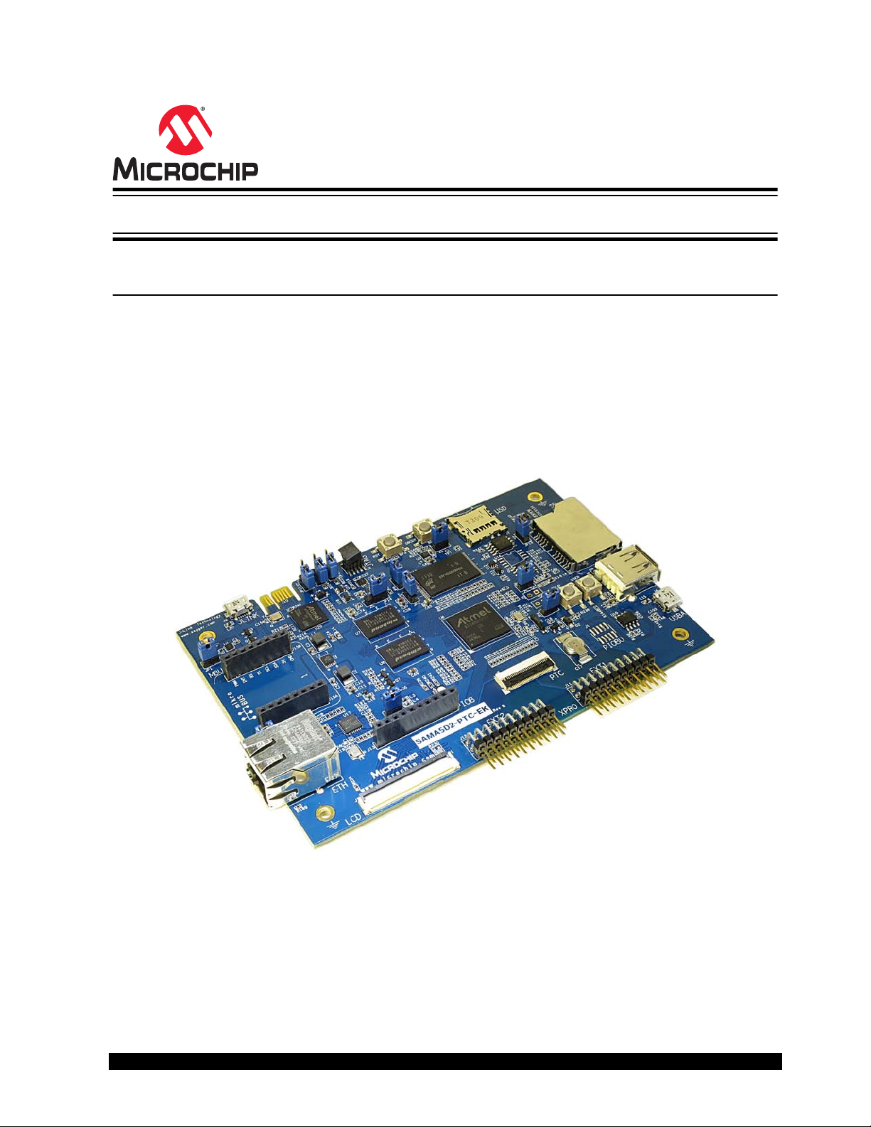
SAMA5D2-PTC-EK
SAMA5D2-PTC-EK User's Guide
Scope
This user's guide describes how to use the SAMA5D2 PTC Evaluation Kit (SAMA5D2-PTC-EK).
The SAMA5D2-PTC-EK is used to evaluate the capabilities of the Peripheral Touch Controller (PTC)
designed for the SAMA5D2 series of embedded MPUs. Refer to the Configuration Summary table in the
SAMA5D2 Series Datasheet for the list of MPUs featuring PTC.
© 2017 Microchip Technology Inc.
DS50002709A-page
1
Page 2

SAMA5D2-PTC-EK
Table of Contents
Scope.............................................................................................................................. 1
1. Introduction................................................................................................................3
1.1. Document Layout......................................................................................................................... 3
1.2. Recommended Reading...............................................................................................................3
2. Product Overview...................................................................................................... 4
2.1. SAMA5D2-PTC-EK Features....................................................................................................... 4
2.2. SAMA5D2-PTC-EK Content.........................................................................................................5
2.3. Evaluation Kit Specifications........................................................................................................ 5
2.4. Power Sources............................................................................................................................. 5
3. Board Components....................................................................................................6
3.1. Board Overview............................................................................................................................6
3.2. Function Blocks............................................................................................................................ 9
3.3. External Interfaces..................................................................................................................... 31
3.4. Debugging Capabilities.............................................................................................................. 35
3.5. PIO Usage on Expansion Connectors........................................................................................40
4. Installation and Operation........................................................................................48
4.1. System and Configuration Requirements...................................................................................48
4.2. Board Setup............................................................................................................................... 48
5. Appendix A. Schematics and Layouts..................................................................... 49
6. Revision History.......................................................................................................62
6.1. Rev. A - 12/2017.........................................................................................................................62
The Microchip Web Site................................................................................................ 63
Customer Change Notification Service..........................................................................63
Customer Support......................................................................................................... 63
Microchip Devices Code Protection Feature................................................................. 63
Legal Notice...................................................................................................................64
Trademarks................................................................................................................... 64
Quality Management System Certified by DNV.............................................................65
Worldwide Sales and Service........................................................................................66
© 2017 Microchip Technology Inc.
DS50002709A-page
2
Page 3

1. Introduction
1.1 Document Layout
The document is organized as follows:
Chapter 1. "Introduction"
•
•
Chapter 2. "Product Overview" – Important information about the SAMA5D2-PTC-EK board
• Chapter 3. "Board Components" – Specifications of the SAMA5D2-PTC-EK and high-level
description of the major components and interfaces
• Chapter 4. "Installation and Operation" – Instructions on how to get started with the SAMA5D2PTC-EK
• Appendix A. "Schematics and Layouts" – SAMA5D2-PTC-EK schematics and layout diagrams
1.2 Recommended Reading
The following Microchip document is available and recommended as a supplemental reference resource:
• SAMA5D2 Series Datasheet. Lit. Number DS60001476
SAMA5D2-PTC-EK
Introduction
© 2017 Microchip Technology Inc.
DS50002709A-page
3
Page 4

2. Product Overview
2.1 SAMA5D2-PTC-EK Features
The SAMA5D2-PTC-EK follows the Microchip MPU strategy for low cost evaluation kits with maximum
reuse capability
This board is mainly dedicated to evaluating the Peripheral Touch Controller capabilities.
Table 2-1. SAMA5D2-PTC-EK Features
Characteristics Specifications Components
, and is built on the SAMA5D2 Xplained Ultra (XUL
SAMA5D2-PTC-EK
Product Overview
T) hardware and software ecosystem.
Processor SAMA5D27-CU (289-ball BGA) 14x14mm
body, 0.8mm pitch
Clock speed
Memory Two 16-bit, 2-Gbit DDR2
Display One LCD interface connector RGB, 18 bits
SD/MMC One standard SD card interface
USB One USB host type A
Ethernet One ETH PHY Micrel KSZ8081RN
Debug Port One JLINK-OB/ JLINK-CDC
MPU: 24 MHz, 32.768 KHz
PHY: Crystal 25 MHz
One 4-Gbit Nand Flash
One QSPI Flash
One Serial Data Flash (optional)
One EEPROM
One microSD card interface
One USB device type MicroAB
One USB HSIC
One JTAG interface
–
–
Winbond W972GG6KB-25
Micron MT29F4G08
Microchip SST26VF064B
Microchip SST26VF032B
Microchip 24AA02E48
With 3.3V/1.8V power switch
–
With 5V power switch
–
Connector not mounted
Embedded JLINK-OB and JLINKCDC (ATSAM3U4C TFBGA100)
Board Monitor One RGB (Red, Green, Blue) LED
Four push button switches
Expansion One set of XPRO WINGS connectors
One ITO FLEX connector
One Port B connector
One PIOBU connector
One mikroBUS connector
© 2017 Microchip Technology Inc.
–
DisableBoot, Reset, WakeUp, User
Free
Dedicated PTC QTouch
Optional
Optional
Optional
–
DS50002709A-page
4
Page 5

Characteristics Specifications Components
Board Supply From USB A and USB JLINK-OB 5VDC
Backup Power Supply SuperCap ELNA DSK-3R3H204T614-H2L
2.2 SAMA5D2-PTC-EK Content
The SAMA5D2-PTC-EK evaluation kit includes the following:
The SAMA5D2-PTC-EK board
•
•
A USB cable
2.3 Evaluation Kit Specifications
Table 2-2. Evaluation Kit Specifications
Characteristic Specification
Board SAMA5D2-PTC-EK
SAMA5D2-PTC-EK
Product Overview
Board supply voltage USB-powered
Temperature Operating: 0°C to +70°C
Relative humidity 0 to 90% (non-condensing)
Main board dimensions 135 × 90 × 20 mm
RoHS status Compliant
Board identification SAMA5D2 Peripheral Touch Controller Evaluation Kit
2.4 Power Sources
Several options are available to power up the SAMA5D2-PTC-EK board:
USB powering through the USB Micro-AB connector (J4 - default configuration)
•
•
Powering through the USB Micro-AB connector on the JLlink-OB Embedded Debugger interface
(J9)
Table 2-3. Electrical Characteristics
Electrical Parameter Value
Input voltage 5VCC
Storage: –40°C to +85°C
Maximum input voltage 6VCC
Maximum 3.3VDC current available 1.2A
I/O voltage 3.3V only
© 2017 Microchip Technology Inc.
DS50002709A-page
5
Page 6
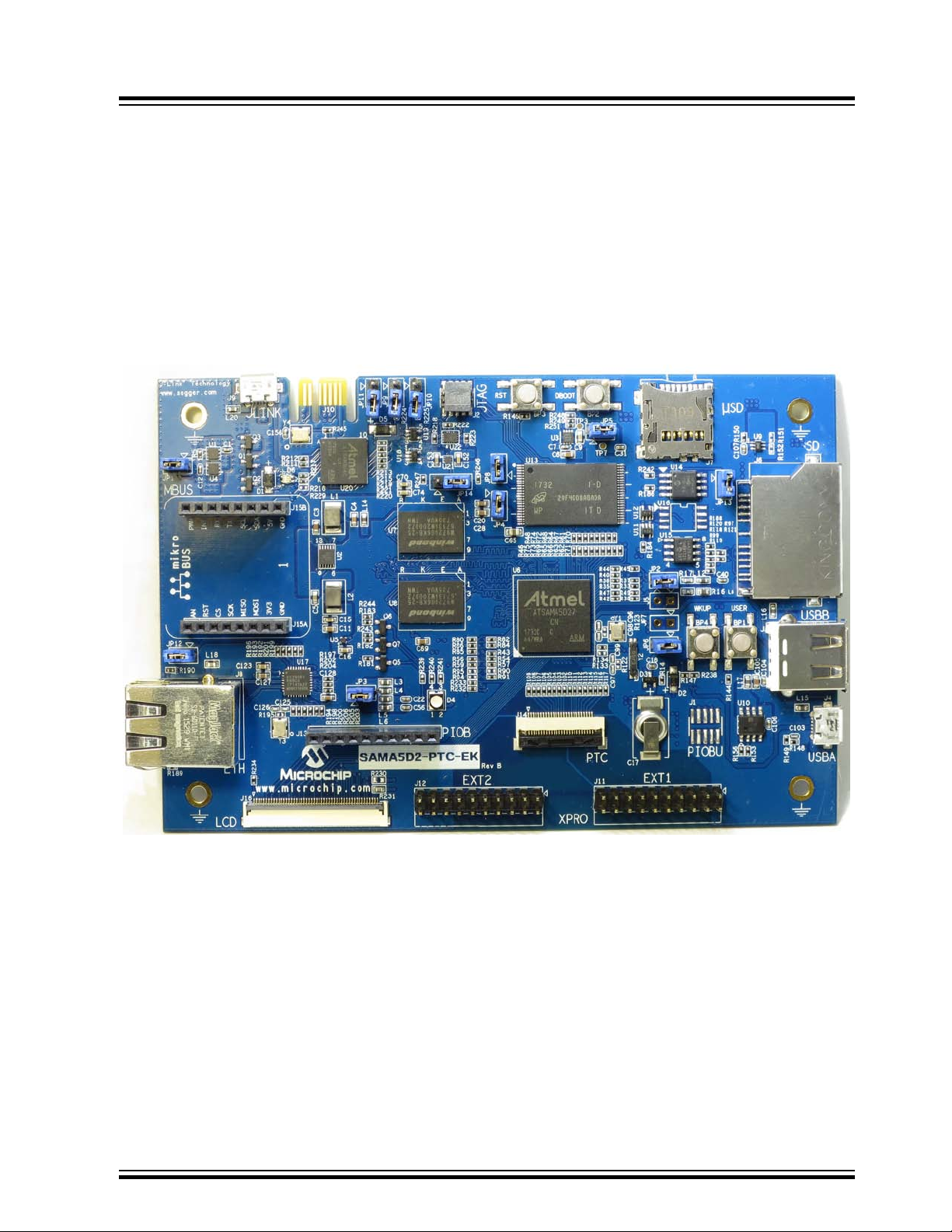
3. Board Components
This section covers the specifications of the SAMA5D2-PTC-EK and provides a high-level description of
the board's major components and interfaces. This document is not intended to provide a detailed
documentation about the processor or about any other component used on the board. It is expected that
the user will refer to the appropriate documents of these devices to access detailed information.
3.1 Board Overview
The fully-featured SAMA5D2-PTC-EK board integrates multiple peripherals and interface connectors, as
shown in the figure below
.
SAMA5D2-PTC-EK
Board Components
3.1.1 Default Jumper Settings
The figure below shows the default jumper settings. Jumpers in red are configuration items and current
measurement points. Jumpers in blue are not populated.
© 2017 Microchip Technology Inc.
DS50002709A-page
6
Page 7
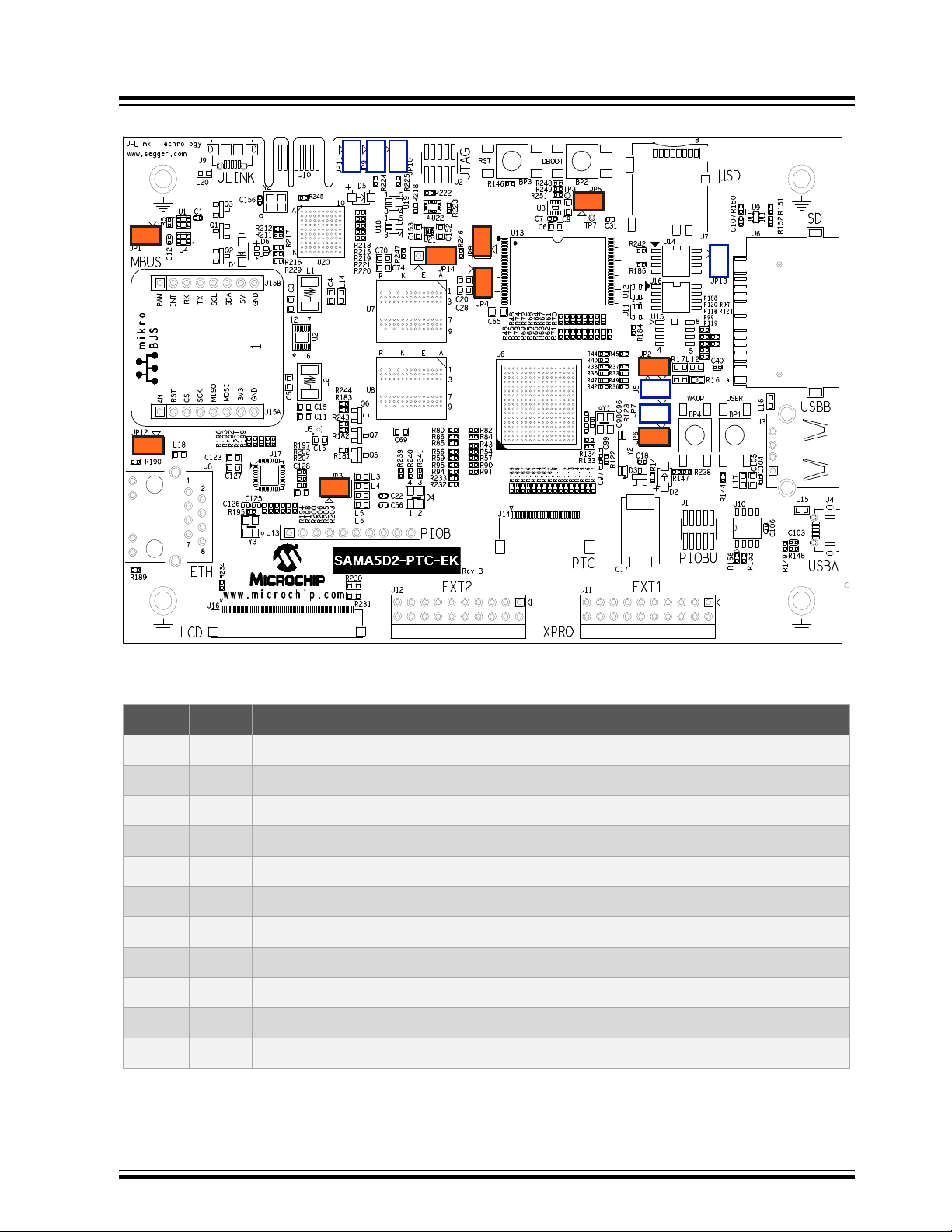
Figure 3-1. Default Jumper Settings
SAMA5D2-PTC-EK
Board Components
The following table describes the functionality of the jumpers.
Table 3-1. SAMA5D2-PTC-EK Jumper Settings
Jumper Default Function
JP1 Closed VDD_MAIN_5V current measurement
JP2 Closed VDDOSC, VDDUTMII, VDDANA, VDDAUDIOPLL current measurement
JP3 Closed VDDISC + VDDIOP0/1/2 current measurement
JP4 Closed VDDIODDR_MPU current measurement
JP5 Closed VDDCORE current measurement
JP6 Closed VDDBU current measurement
JP7 Open PIOBU1, PIOBU7
JP8 Closed Disables NAND_CS (open=disable)
JP9 Open Enables JTAG-CDC (closed=disable)
JP10 Open Enables JTAG-OB (closed=disable)
JP11 Open Erases SAM3U Flash Code (closed = erase)
© 2017 Microchip Technology Inc.
DS50002709A-page 7
Page 8
Jumper Default Function
WARNING
JP12 Closed Powers mikroBUS extension (3.3V)
JP13 Open Disables QSPI
JP14 1-2 Enables 3.3V JLINK-OB, connected to shutdown circuitry
2-3 Enables 3.3V JLINK-OB, always ON
3.1.2 Connectors on Board
The following table describes the interface connectors on the SAMA5D2-PTC-EK.
Table 3-2. SAMA5D2-PTC-EK Board Interface Connectors
Connector Interfaces to
SAMA5D2-PTC-EK
Board Components
Warning: This jumper is reserved for factory configuration and should
never be used by the end user.
J1 PIOBU, tamper and analog comparator connector (not populated)
J2 JTAG, 10-pin IDC connector
J3 USB Host B. Supports USB host using a type A connector
J4 USB A Device. Supports USB device using a type Micro-AB connector
J5 USB-C HSIC header (not populated)
J6 Standard SDMMC connector
J7 microSD connector
J8 Ethernet 10/100 RJ45
J9 USB-A MicroAB, JLink-OB port
J10 PCB connector for factory-programming the JLINK-OB/SAM3U
J11, J12 Xplained Pro expansion connectors (PTC-dedicated add-on boards)
J13 PIOs PortB connector
J14 ITO connector
J15 A&B mikroBUS connector
J16 Expansion TFT LCD connector for display module
© 2017 Microchip Technology Inc.
DS50002709A-page
8
Page 9
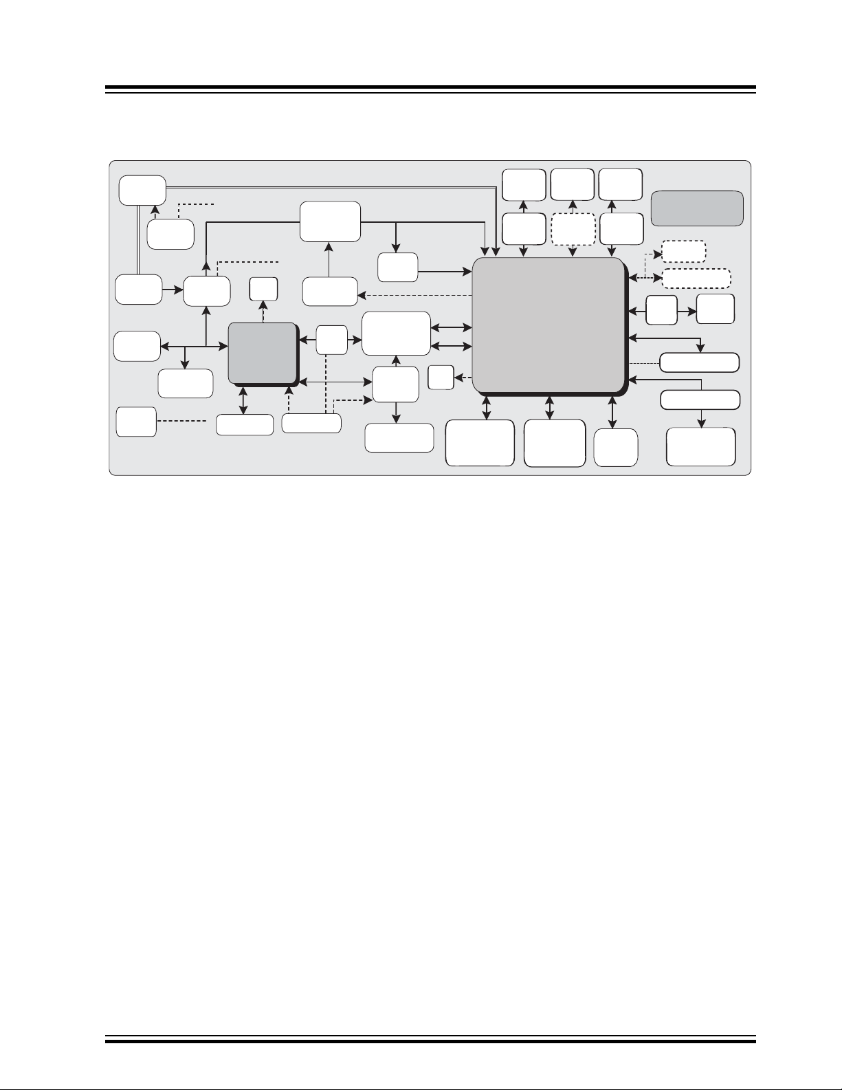
3.2 Function Blocks
POWER
MONITOR
JLINK-OB
JTAG Interface
JLINK Power
5v/3v3
USB
Connector
Function Select
System Supplies
POWER
REGULATORS
SHDN
UART
MPU JTAG
Interface
JTAG
Switch
JTAG
LCD (18bits)
TWI/SPI
RJ45
USB A&B
SDHC0
SDHC1
SAMA5D2-PTC-EK
Push
Button
FPC Connector
DEBUG
Interface
Reset, Wkup
DisBoot, User
SD Card
Connector
uSD
Connector
3v3, 2v5,1v8, 1v2
VDDBU
GPIO
USB
Detection
ETH
PHY
PTC
QSPI
Flash
DDR2
SDRAM
DDR2
SDRAM
Power
Cap
Serial
EEprom
Nand
Flash
PIOBU Connector
MikroBUS
Interface
ITO Connector
XPRO (1&2)
PTC Interface
GPIO
PortB[0-7]
Power
Switch
VBUS
5v
5v
5v
USB-B
Connector
USB-A
Connector
SPI
Flash
Leds
JLINK-OB
JLINK-CDC
SAMA5D27
RGB
Leds
Tri
State
Figure 3-2. SAMA5D2-PTC-EK Block Diagram
SAMA5D2-PTC-EK
Board Components
3.2.1 Processor
The SAMA5D2 Series is a high-performance, power-efficient embedded MPU based on the ARM
Cortex®-A5 processor.
Please refer to the SAMA5D2 Series datasheet for more information.
3.2.2 Power Supply T
3.2.2.1 Input Power Options
Two options are available to power the SAMA5D2-PTC-EK board. The USB-powered operation is the
default configuration and comes from the USB device ports (J4-J9) connected to a PC or a 5VDC supply.
Such USB power source is sufficient to supply the board in most applications. It is important to note that
when the USB-powered operation is used, the USB port down the way has a limited powering capability.
If the USB-B Host port (J3) is required to provide full powering capabilities to the target application, it is
recommended to use an external DC supply instead of a USB power source.
The following figure is a schematic of the power options.
© 2017 Microchip Technology Inc.
opology and Power Distribution
®
DS50002709A-page 9
Page 10

VDD_MAIN_5V
GND_POWER
GND_POWER
GND_POWER
GND_POWER
GND_POWER
VBUS_USBA
VBUS_JLINK
U1A
DMP2160UFD
1
2
6
7
C1
100nF
C0402
U4A
DMP2160UFD
1
2
6
7
R5 100K
R0402
R6 DNP
R0402
U1B
DMP2160UFD
4
5
3
8
JP1
Header 1X2
1
2
C12
100nF
C0402
R1
10K
R0402
U4B
DMP2160UFD
4
5
3
8
R2
100K
R0402
JPR1
Jumper
C2
100nF
C0402
CAUTION
SAMA5D2-PTC-EK
Board Components
Figure 3-3. Input Powering
Note: USB-powered operation eliminates additional wires and batteries. It is the preferred mode of
operation for any project that requires only a 5V source at up to 500 mA.
Jumper JP1 is used to perform MAIN_5V current measurements on the SAMA5D2-PTC-EK board.
3.2.2.2 Power Supply Requirements and Restrictions
Detailed information on the device power supplies is provided in tables “SAMA5D2 Power Supplies” and
“Power Supply Connections” in the SAMA5D2 Series datasheet.
3.2.2.3 Power-up and Power-down Considerations
Power-up and power-down considerations are described in section “Power Considerations” of the
SAMA5D2 Series datasheet.
Caution: The power-up and power-down sequences provided in the SAMA5D2 Series
datasheet must be respected for reliable operation of the device.
3.2.2.4 Power Management
The board power management uses three types of regulators:
• One dual synchronous step-down DC-DC regulator (U2 MIC2230) generates the 3.3V/800mA and
1.8V/800mA power lines and utilizes a high-ef
PWM control architecture that requires a minimum number of external components.
• One ultra low-dropout linear regulator (U3 MIC47053) generates the 1.25V/500mA from the 1.8V
source.
• One high-performance single 2.5V/150mA is used as a VDDFUSE generator (U5 MIC5366).
The main regulators are enabled through a Field Effect Transistor (FET) scheme. The processor can
assert SHDN (a VDDBU-powered I/O) to shut down the regulators to enter Backup mode. All regulators
on the board are also shut down by the action of the SHDN signal.
A 3.3V battery (supercap) is implemented to permanently maintain VDDBU voltage (note: jumper JP6
must be in place). The board can be woken up by action on the PB4 button, which drives the WKUP
signal (also a VDDBU-powered I/O).
The figure below shows the power management scheme.
© 2017 Microchip Technology Inc.
ficiency, fixed-frequency (2.5 MHz), current-mode
DS50002709A-page
10
Page 11
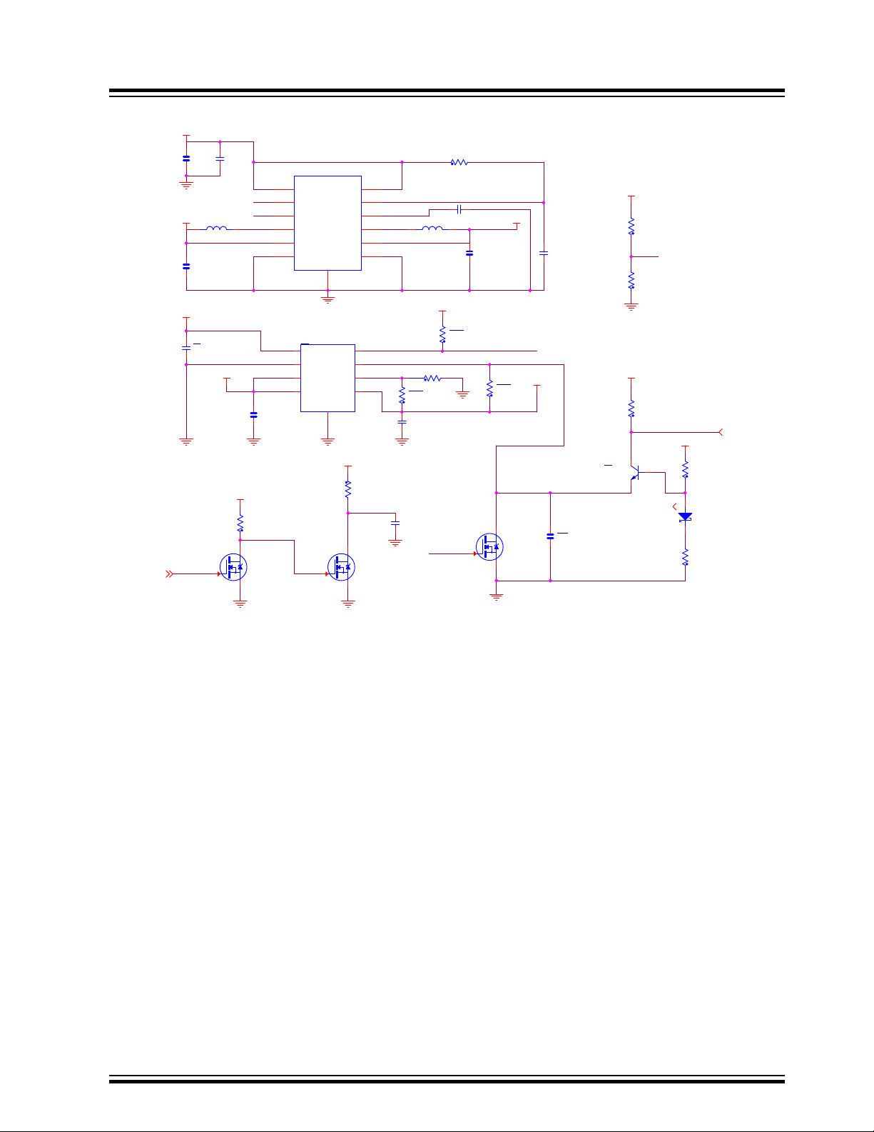
Figure 3-4. Board Power Management
EN_1
EN_VDD_1V25
STARTB
STARTB
FPWM#
FPWM#
EN_1
EN_VDD_1V25
VDD_MAIN_5V
GND_POWER
GND_POWER
VDD_3V3VDD_1V8
VDD_MAIN_5V
VDD_1V8
VDD_1V25
VDD_MAIN_5V
GND_POWER GND_POWER
GND_POWER
VDD_MAIN_5V
VDD_3V3
VDD_MAIN_5V
GND_POWER
VDD_3V3
GND_POWER
GND_POWER
VDD_3V3
GND_POWER
GND_POWERGND_POWER
GND_POWER
SHDN
C4
10uF
C0603
U2
MIC2230-GSYML
MLF3x3mm
AVIN
3
EN1
11
FPWM#
7
SW1
8
OUT1
12
AGND5PGND
6
OUT2
1
SW2
4
PGOOD
10
EN2
2
VIN
9
EPAD
13
R249 4.7K
R0402
R13
39K
R0402
C6
10uF
C0603
R3
100K
R0402
R251
10K
R0402
R12
220K
R0402
C10 390pF
C0402
C7
100nF
C0402
L2 LQH43CN2R2M03L
L1812
C3
10uF
C0603
R248
20K
R0402
R10
DNP
R0402
R11
100K
R0402
C13
4.7nF
C0402
R250
3.3K
R0402
L1 LQH43CN2R2M03L
L1812
C5
1uF
C0603
Q1
BSS138
SOT23_123
1
3
2
R4
10K
R0402
C9
1uF
C0603
D1
PMEG6010CEGWX
sod123
Q2
BSS138
SOT23_123
1
3
2
C8
100nF
C0402
R9
100K
R0402
C11
10uF
C0603
Q3
BSS138
SOT23_123
1
3
2
U3
MIC47053YMT
BIAS
1
GND
2
IN1
3
IN2
4
ADJ
6
OUT
5
EPAD
9
PGOOD
7
EN
8
Q4
BC847C
SOT-23
1
32
R8 100K
R0402
C14
2.2uF
C0603
NRST
SAMA5D2-PTC-EK
Board Components
3.2.2.5 Supply Group Configuration
The main regulators provide all power supplies required by the SAMA5D2 device:
• 1.25V VDDCORE, VDDPLLA, VDDUTMIC, VDDHSIC
• 1.8V VDDIODDR, VDDSDHC1V8
• 2.5V VDDFUSE
• 3.3V VDDIOP0, VDDIOP1, VDDIOP2, VDDISC
• 3.3V VDDOSC, VDDUTMI, VDDANA, VDDAUDIOPLL
• 3.3V VDDBU
© 2017 Microchip Technology Inc.
DS50002709A-page
11
Page 12

Figure 3-5. Power Lines Distribution
For DDR2 For MPU
VDDHSIC
V
DD_3V3
VDD_1V25
VDDCORE
VDDIOP0
VDDIOP2
VDDIOP1
VDDPLLA
VDDUTMIC
VDDIODDR
VDDAUDIOPLL
VDDANA
VDDOSC
VDDUTMII
VDDISC
VDD_1V8 VDDSDHC1V8
L3
BLM18PG181SN1D
R0603
1 2
R16
2R2
R0603
R15
2R2
R0603
R17
0R
R0603
L7
MLZ1608N100L
L0603
L11
BLM18PG181SN1D
R0603
1 2
L10
BLM18PG181SN1D
R0603
1
2
JP5
Header 1X2
1
2
R18
0R
R0603
L4
BLM18PG181SN1D
R0603
1 2
L14
BLM18PG181SN1D
1
2
L9
MLZ1608N100L
L0603
JP4
Header 1X2
1
2
L13
BLM18PG181SN1D
R0603
1 2
L6
BLM18PG181SN1D
R0603
1
2
L8
MLZ1608N100L
L0603
R19
2R2
R0603
L5
BLM18PG181SN1D
R0603
1 2
L12
BLM18PG181SN1D
R0603
1 2
JP3
Header 1X2
1
2
JP2
Header 1X2
1
2
(3V3)
(1V2)
(1V8)
(3V3)
)3
V3(
)3V3()3V3
(
)5V2(
)
2V1(
(3V3)
(3V3)
(3V3)
(3V3)
(3V3)
(3V3)
(3V3)
(3V3)
(3V3)
(1V8)
(1V2)
(1V2)
(1V2)
(1V2)
(2V5)
(3V3)
(1V2)
)3
V3(
)2V1(
(3V3)
(3V3)
(3V3 or 1V8)
(3V3 or 1V8)
VDDBU
VDDCORE
VDDPLLA
VDDIOP0
VDDIOP1
VDDIOP2
VDDHSIC
VDDUTMIC
VDDUTMII
VDDSDHC
VDDPLLA
VDDOSC
VDDISC
VDDFUSE
VDDAUDIOPLL
VDDBU
VDDIODDR
VDDANA
VDDANA
VDDIOP0
VDDIOP1
VDDIOP2
VDDHSIC
VDDFUSE
VDDUTMII
VDDSDHC
VDDOSC VDDISC
VDDUTMIC
VDDCORE
VDDIODDR
VDDAUDIOPLL
GND_POWER
VDDBU
GND_POWER
GND_POWER
VDDCORE
GND_POWER
VDDIODDR
VDDANA
GND_POWER
VDDIOP0
GND_POWER
VDDIOP1
GND_POWER
VDDIOP2
GND_POWER
VDDHSIC
GND_POWER
VDDFUSE
GND_POWER
VDDUTMII
GND_POWER
VDDSDHC
GND_POWER
VDDPLLA
GND_POWER
VDDOSC
VDDISC
GND_POWER
GND_POWER
VDDUTMIC
GND_POWER
GNDUTMII
GND_POWER
VDDAUDIOPLL
C35
100nF
C0402
C51
1nF
C0402
C54
4.7uF
C0805
C31
100nF
C0402
C25
4.7uF
C0805
C61
1nF
C0402
C56
100nF
C0402
C37
100nF
C0402
C59
1nF
C0402
C20
10uF
C0603
C19
10uF
C0603
C21
100nF
C0402
C42
100nF
C0402
C40
100nF
C0402
C52
1nF
C0402
C50
100nF
C0402
C48
100nF
C0402
C26
100nF
C0402
C53
100nF
C0402
C28
10uF
C0603
C30
100nF
C0402
C34
100nF
C0402
C60
1nF
C0402
C46
100nF
C0402
C41
4.7uF
C0805
C49
100nF
C0402
C27
10uF
C0603
C44
100nF
C0402
R20
1R-1%
R0603
C29
100nF
C0402
C36
100nF
C0402
R21
1R-1%
R0603
C24
4.7uF
C0805
C47
100nF
C0402
C32
100nF
C0402
ATSAMA5D27C-CN
U6G
bga289p8
GNDADC
K5
GNDANA
L3
GNDBU
N6
GNDCORE_1
E7
GNDCORE_2
E9
GNDCORE_3
H4
GNDCORE_4
K12
GNDCORE_5
M5
GNDCORE_6
M9
GNDDDR_1
D14
GNDDDR_2
E11
GNDDDR_3
E12
GNDDDR_4
E14
GNDDDR_5
H14
GNDDDR_6
J14
GNDDDR_7
L14
GNDDPLL
T5
GNDAUDIOPLL
T4
GNDIOP0_1
F6
GNDIOP0_2
G7
GNDIOP1_1
M13
GNDIOP1_2
P14
GNDIOP2
F9
GNDISC
G4
GNDOSC
T6
GNDPLLA
U5
GNDSDMMC
R11
GNDUTMII
P9
GNDUTMIC
R7
VDDADC
L5
VDDANA
K3
VDDBU
N7
VDDCORE_1
D7
VDDCORE_2
D9
VDDCORE_3
H3
VDDCORE_4
K13
VDDCORE_5
N5
VDDCORE_6
N9
VDDDDR_1
D11
VDDDDR_2
D12
VDDDDR_3
D15
VDDDDR_4
E15
VDDDDR_5
H15
VDDDDR_6
J15
VDDDDR_7
L15
VDDAUDIOPLL
T3
VDDFUSE
M12
VDDHSIC
R9
VDDIOP0_1
E6
VDDIOP0_2
F7
VDDIOP1_1
N13
VDDIOP1_2
R14
VDDIOP2
F10
VDDISC
F4
VDDOSC
T7
VDDPLLA
U4
VDDSDMMC
P11
VDDUTMII
P8
VDDUTMIC
P7
C55
100nF
C0402
C23
100nF
C0402
C43
100nF
C0402
C38
100nF
C0402
C58
1nF
C0402
C57
100nF
C0402
C33
100nF
C0402
C39
100nF
C0402
C45
100nF
C0402
C22
100nF
C0402
Figure 3-6. Processor Power Lines Supplies
SAMA5D2-PTC-EK
Board Components
3.2.2.6 VDDFUSE
The SAMA5D2-PTC-EK board embeds a 2.5V regulator for fuse box programming.
© 2017 Microchip Technology Inc.
DS50002709A-page
12
Page 13
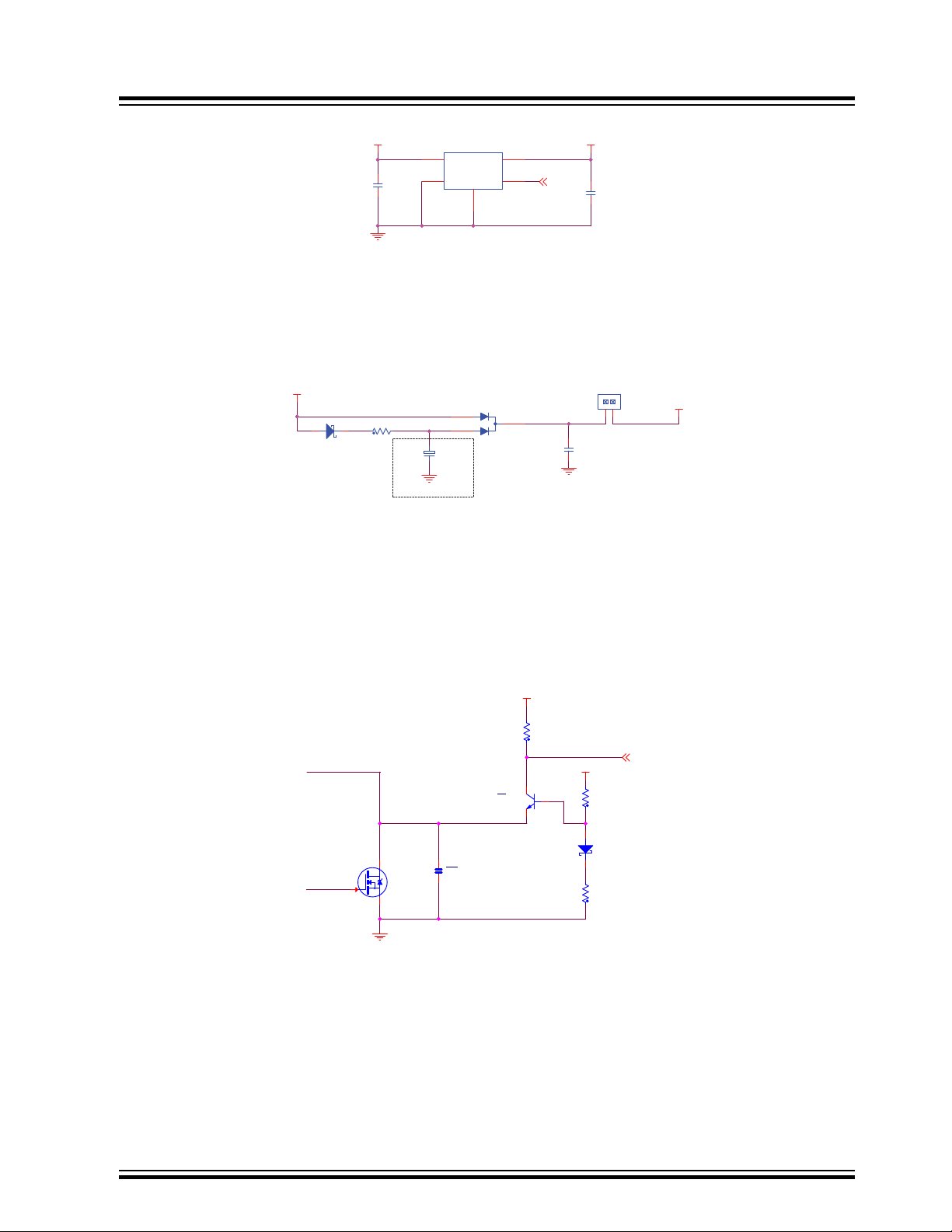
Figure 3-7. VDDFUSE Regulator
VDD_3V3
GND_POWER
VDDFUSE
EN_1 12
C16
1uF
C0603
U5
MIC5366-2.5YMT
MLF1x1mm
VIN
4
GND
2
VOUT
1
EN
3
EPAD
5
C15
1uF
C0603
(Super)-Capa citor
energy storage
VDDBU
GND_POWER
GND_POWER
VDD_3V3
C18
100nF
C0402
JP6
Header 1X2
1
2
+
C17
0.2F/3.3V
c117x68
D2
PMEG6010CEGWX
sod123
R14 100R-1%
R0402
D3
BAT54C
SOT23_123
3
1
2
STARTB
GND_POWER
VDD_MAIN_5V
VDD_3V3
NRST
R13
39K
R0402
R12
220K
R0402
R11
100K
R0402
D1
PMEG6010CEGWX
sod123
Q3
BSS138
SOT23_123
1
3
2
Q4
BC847C
SOT-23
1
32
C14
2.2uF
C0603
PowerGood VDD_1V25
3.2.2.7 Backup Power Supply
The SAMA5D2-PTC-EK board requires a power source in order to permanently power the backup part of
the SAMA5D2 device (refer to SAMA5D2 Series datasheet). The super capacitor C17 sustains such
permanent power to VDDBU when all system power sources are off.
Figure 3-8. VDDBU Powering Options
SAMA5D2-PTC-EK
Board Components
3.2.3 Reset Circuitry
3.2.4 Shutdown Circuitry
The reset sources for the SAMA5D2-PTC-EK board are:
• Power-on reset from the power management unit,
Push button reset BP3,
•
• JTAG or JLINK-OB reset from an in-circuit emulator.
Figure 3-9. Main Reset Control
The SHDN signal, output of Shutdown Controller (SHDN), drives the shutdown request to the power
. This output signal is supplied by VDDBU, which is present in Backup mode.
supply
The Shutdown Controller manages the main power supply and is connected to the ENABLE input pin of
the DC/DC converter providing the main power supplies of the system.
© 2017 Microchip Technology Inc.
DS50002709A-page
13
Page 14

Figure 3-10. Shutdown Controller
STARTB
EN_1
VDD_MAIN_5V
GND_POWER GND_POWER
VDD_3V3
GND_POWER
SHDN
R3
100K
R0402
Q1
BSS138
SOT23_123
1
3
2
R4
10K
R0402
Q2
BSS138
SOT23_123
1
3
2
C8
100nF
C0402
WAKE UP
RESET
DIS BOOT
GND_POWER
VDDBU
DISABLE_BOOT
NRST
WKUP
R146 100R-1%
r0402
BP3 Tact Switch
FSM2JSML
R147 100R-1%
r0402
R238 10K
R0402
BP2 Tact Switch
FSM2JSML
R145 100R-1%
r0402
BP4 Tact Switch
FSM2JSML
USER BUTTON
PA10_USER_BT
R144 0R
R0402
BP1 Tact Switch
FSM2JSML
GND_POWER
3.2.5 Push Button Switches
The SAMA5D2-PTC-EK features four push buttons:
• One board reset push button (BP3). When pressed and released, it causes a power-on reset of the
board.
•
One wakeup push button (BP4) connected to the SAMA5D2 WKUP pin, used to exit the processor
from low-power mode.
• One disable boot push button (BP2) used to devalidate the boot memories (refer to CS Disable).
Figure 3-11. System Push Buttons
SAMA5D2-PTC-EK
Board Components
• One user push button (BP1) connected to PIO PB10.
Figure 3-12. User Push Button
3.2.6 Clock Circuitry
The embedded microcontroller generates its necessary clocks based on two crystal oscillators: one slow
clock (SLCK) oscillator running at 32.768 KHz and one main clock oscillator running at 24 MHz.
The SAMA5D2-PTC-EK board includes four clock sources:
• The two clocks mentioned above are alternatives for the SAMA5D2 processor (24 MHz, 32.768
kHz)
•
One crystal oscillator for the Ethernet RMII chip (25 MHz)
• One crystal oscillator for the JLink-OB microcontroller (12 MHz)
© 2017 Microchip Technology Inc.
DS50002709A-page
14
Page 15

Figure 3-13. MPU Clock Circuitry
XIN
XOUT
XOUT32
XIN32
GND_POWERGND_POWER
GND_POWER
GND_POWER
R122
DNP
R0402
C98
20pF
C0402
C97
20pF
C0402
R123 DNP
R0402
C96
20pF
C0402
Y1
24MHz CL=10pF
x4s32x25
1 4
32
C99
20pF
C0402
Y2
32.768KHz CL=12.5pF
X4S70X15
1
23
4
3.2.7 Memory
3.2.7.1 Memory Organization
The SAMA5D2 features a DDR/SDR memory interface and an External Bus Interface (EBI) to enable
interfacing to a wide range of external memories and to almost any kind of parallel peripheral.
This section describes the memory devices mounted on the SAMA5D2-PTC-EK board:
wo DDR2 SDRAMs
• T
• One NAND Flash
• One QSPI Flash
• One SPI Flash (optional)
• One serial EEPROM
SAMA5D2-PTC-EK
Board Components
Additional memory can be added to the board by:
• Installing an SD or MMC card in the SD/MMC0 or SD/MMC1 slot,
• Using the USB-B port.
Support is dependent upon driver support in the OS.
3.2.7.2 DDR2/SDRAMs
Two DDR2/SDRAMs (W972GG6KB-25-2 Gbits = 16 Mbits x 16 x 8 banks) are used as main system
memory, totalling 4 Gbits of SDRAM on the board. The memory bus is 32 bits wide and operates with a
frequency of up to 166 MHz.
The figure below illustrates the implementation for the DDR2 memories.
© 2017 Microchip Technology Inc.
DS50002709A-page
15
Page 16
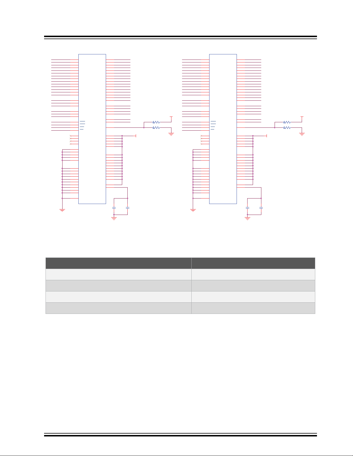
Figure 3-14. DDR2 SDRAMs
DDR_VREFDDR_VREF
DDR_DQM0
DDR_DQM1
DDR_DQM2
DDR_DQM3
DDR_DQS0-
DDR_DQS0+
DDR_DQS1+
DDR_DQS1-
DDR_DQS2+
DDR_DQS2DDR_DQS3+
DDR_DQS3-
DDR_BA1
DDR_BA0
DDR_BA1
DDR_BA0
DDR_WE DDR_WE
DDR_CSDDR_CS
DDR_CLK-
DDR_CLK+
DDR_CLK-
DDR_CLK+
DDR_CKE DDR_CKE
DDR_CAS
DDR_RAS
DDR_CAS
DDR_RAS
DDR_D16
DDR_D17
DDR_D18
DDR_D19
DDR_D20
DDR_D21
DDR_D22
DDR_D23
DDR_D24
DDR_D25
DDR_D26
DDR_D27
DDR_D28
DDR_D29
DDR_D30
DDR_D31
DDR_D0
DDR_D1
DDR_D2
DDR_D3
DDR_D4
DDR_D5
DDR_D6
DDR_D7
DDR_D8
DDR_D9
DDR_D10
DDR_D11
DDR_D12
DDR_D13
DDR_D14
DDR_D15
DDR_A0
DDR_A1
DDR_A2
DDR_A3
DDR_A4
DDR_A5
DDR_A6
DDR_A7
DDR_A8
DDR_A9
DDR_A10
DDR_A11
DDR_A12
DDR_A0
DDR_A1
DDR_A2
DDR_A3
DDR_A4
DDR_A5
DDR_A6
DDR_A7
DDR_A8
DDR_A9
DDR_A10
DDR_A11
DDR_A12
DDR_BA2 DDR_BA2
DDR_A13DDR_A13
GND_POWER
VDD_1V8
GND_POWER
VDD_1V8
GND_POWER
GND_POWER
VDD_1V8
GND_POWER
VDD_1V8
GND_POWER
C94
100nF
C0402
R29 DNP R0402
C95
1nF
C0402
U8
W972GG6KB-25
bga84-32-1509e
A0
M8
A1
M3
A2
M7
A3
N2
A4
N8
A5
N3
A6
N7
A7
P2
A8
P8
A9
P3
A10
M2
A11
P7
A12
R2
A13
R8
BA0
L2
BA1
L3
BA2
L1
CKE
K2
CK_P
J8
CK_N
K8
RAS
K7
CAS
L7
WE
K3
CS
L8
DQ0
G8
DQ1
G2
DQ2
H7
DQ3
H3
DQ4
H1
DQ5
H9
DQ6
F1
DQ7
F9
DQ8
C8
DQ9
C2
DQ10
D7
DQ11
D3
DQ12
D1
DQ13
D9
DQ14
B1
DQ15
B9
LDQS_P
F7
NU/LDQS_N
E8
UDQS_P
B7
NU/UDQS_N
A8
LDM
F3
UDM
B3
ODT
K9
NC1
A2
NC2
E2
NC3
R3
NC4
R7
VDD1
A1
VDD2
E1
VDD3
J9
VDD4
M9
VDD5
R1
VDDQ1
A9
VDDQ2
C1
VDDQ3
C3
VDDQ4
C7
VDDQ5
C9
VDDQ6
E9
VDDQ7
G1
VDDQ8
G3
VDDQ9
G7
VDDQ10
G9
VDDL
J1
VREF
J2
VSS1
A3
VSS2
E3
VSS3
J3
VSS4
N1
VSS5
P9
VSSQ1
A7
VSSQ2
B2
VSSQ3
B8
VSSQ4
D2
VSSQ5
D8
VSSQ6
E7
VSSQ7
F2
VSSQ8
F8
VSSQ9
H2
VSSQ10
H8
VSSDL
J7
U7
W972GG6KB-25
bga84-32-1509e
A0
M8
A1
M3
A2
M7
A3
N2
A4
N8
A5
N3
A6
N7
A7
P2
A8
P8
A9
P3
A10
M2
A11
P7
A12
R2
A13
R8
BA0
L2
BA1
L3
BA2
L1
CKE
K2
CK_P
J8
CK_N
K8
RAS
K7
CAS
L7
WE
K3
CS
L8
DQ0
G8
DQ1
G2
DQ2
H7
DQ3
H3
DQ4
H1
DQ5
H9
DQ6
F1
DQ7
F9
DQ8
C8
DQ9
C2
DQ10
D7
DQ11
D3
DQ12
D1
DQ13
D9
DQ14
B1
DQ15
B9
LDQS_P
F7
NU/LDQS_N
E8
UDQS_P
B7
NU/UDQS_N
A8
LDM
F3
UDM
B3
ODT
K9
NC1
A2
NC2
E2
NC3
R3
NC4
R7
VDD1
A1
VDD2
E1
VDD3
J9
VDD4
M9
VDD5
R1
VDDQ1
A9
VDDQ2
C1
VDDQ3
C3
VDDQ4
C7
VDDQ5
C9
VDDQ6
E9
VDDQ7
G1
VDDQ8
G3
VDDQ9
G7
VDDQ10
G9
VDDL
J1
VREF
J2
VSS1
A3
VSS2
E3
VSS3
J3
VSS4
N1
VSS5
P9
VSSQ1
A7
VSSQ2
B2
VSSQ3
B8
VSSQ4
D2
VSSQ5
D8
VSSQ6
E7
VSSQ7
F2
VSSQ8
F8
VSSQ9
H2
VSSQ10
H8
VSSDL
J7
C72
100nF
C0402
R32 0R
R0402
C75
1nF
C0402
R31
DNP R0402
R30 0R
R0402
SAMA5D2-PTC-EK
Board Components
3.2.7.3 DDR_CAL Analog Input
One specific analog input, DDR_CAL, is used to calibrate all DDR I/Os.
Table 3-3.
Calibration Cell DDR_CAL Value
Memory Resistor value
LPDDR2/LPDDR3 24K
DDR3L 23K
DDR3 22K
DDR2/LPDDR1 21K
© 2017 Microchip Technology Inc.
DS50002709A-page
16
Page 17
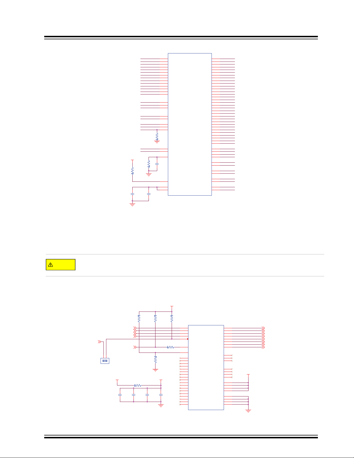
Figure 3-15. DDR Signals and CAL Analog Input
DDR_D0
DDR_D1
DDR_D2
DDR_D3
DDR_D4
DDR_D5
DDR_D6
DDR_D7
DDR_D8
DDR_D9
DDR_D10
DDR_D11
DDR_D12
DDR_D13
DDR_D14
DDR_D15
DDR_D16
DDR_D17
DDR_D18
DDR_D19
DDR_D20
DDR_D21
DDR_D22
DDR_D23
DDR_D24
DDR_D25
DDR_D26
DDR_D27
DDR_D28
DDR_D29
DDR_D30
DDR_D31
DDR_DQM0
DDR_DQM1
DDR_DQM2
DDR_DQM3
DDR_DQS0+
DDR_DQS0-
DDR_DQS1+
DDR_DQS1-
DDR_DQS2+
DDR_DQS2-
DDR_DQS3+
DDR_DQS3-
DDR_A0
DDR_A1
DDR_A2
DDR_A3
DDR_A4
DDR_A5
DDR_A6
DDR_A7
DDR_A8
DDR_A9
DDR_A10
DDR_A11
DDR_A12
DDR_A13
DDR_BA0
DDR_BA1
DDR_RAS
DDR_CAS
DDR_BA2
DDR_CS
DDR_WE
DDR_VREF
DDR_RESETN
DDR_CLK+
DDR_CLKDDR_CKE
GND_POWER
GND_POWER
GND_POWER
VDDIODDR
R23
100K
R0402
R24
21K-1%
R0402
R25
100K
R0402
C64
22pF
C0402
ATSAMA5D27C-CN
U6E
bga289p8
DDR_A0
F12
DDR_A1
C17
DDR_A10
C15
DDR_A11
A16
DDR_A12
A17
DDR_A13
G11
DDR_A2
B17
DDR_A3
B16
DDR_A4
C16
DDR_A5
G14
DDR_A6
F14
DDR_A7
F11
DDR_A8
C14
DDR_A9
D13
DDR_BA0
H12
DDR_BA1
H13
DDR_BA2
F17
DDR_CAL
E13
DDR_CAS
G12
DDR_CKE
F16
DDR_CLK
E17
DDR_CLKN
D17
DDR_CS
G13
DDR_D0
B12
DDR_D1
A12
DDR_D10
H17
DDR_D11
K17
DDR_D12
K16
DDR_D13
J13
DDR_D14
K14
DDR_D15
K15
DDR_D16
B8
DDR_D17
B9
DDR_D18
C9
DDR_D19
A9
DDR_D2
C12
DDR_D20
A10
DDR_D21
D10
DDR_D22
B11
DDR_D23
A11
DDR_D24
J12
DDR_D25
H10
DDR_D26
J11
DDR_D27
K11
DDR_D28
L13
DDR_D29
L11
DDR_D3
A13
DDR_D30
L12
DDR_D31
M17
DDR_D4
A14
DDR_D5
C13
DDR_D6
A15
DDR_D7
B15
DDR_D8
G17
DDR_D9
G16
DDR_DQM0
C11
DDR_DQM1
G15
DDR_DQM2
C8
DDR_DQM3
H11
DDR_DQS0
B13
DDR_DQS1
J17
DDR_DQS2
C10
DDR_DQS3
L17
DDR_DQSN0
B14
DDR_DQSN1
J16
DDR_DQSN2
B10
DDR_DQSN3
L16
DDR_RAS
F13
DDR_RESETN
E16
DDR_VREFCM
D16
DDR_VREFB0
H16
DDR_WE
F15
C62
100nF
C0402
C63
100nF
C0402
CAUTION
NAND_WPn
3V3_NAND
VDD_3V3 3V3_NAND
3V3_NAND
NAND_CLE_PB1
NAND_ALE_PB0
NAND_REn_PB2
NAND_WEn_PA30
NAND_RDY_PC8
NAND_IO5_PA27
NAND_IO6_PA28
NAND_IO7_PA29
NAND_IO0_PA22
NAND_IO1_PA23
NAND_IO2_PA24
NAND_IO3_PA25
NAND_IO4_PA26
NAND_CS_PA31
R175
100K
MT29F4G08ABADAWP
U13
NC1
1
NC2
2
NC3
3
NC4
4
NC5
5
NC6
6
R/B#
7
CE#
9
NC7
10
VCC_1
12
VSS_1
13
NC9
14
NC10
15
CLE
16
ALE
17
NC21
47
VSS_4
48
RE#
8
NC8
11
WE#
18
WP#
19
DNU2
20
DNU1
21
NC11
22
NC12
23
NC13
24
VSS_2
25
NC14
26
NC15
27
NC16
28
DQ0
29
DQ1
30
DQ2
31
DQ3
32
NC17
33
VCC_2
34
DNU3
35
VSS_3
36
VCC_3
37
DNU4
38
VCC_4
39
NC18
40
DQ4
41
DQ5
42
DQ6
43
DQ7
44
NC19
45
NC20
46
R177
DNP
R174 0R
C113
100nF
R180
100K
C112
100nF
JP8
Header 1X2
1
2
C114
100nF
R179 0R
C115
100nF
R176
10K
SAMA5D2-PTC-EK
Board Components
3.2.7.4 NAND FLASH
The SAMA5D2-PTC-EK has native support for NAND Flash memory through its NAND Flash Controller.
The board implements one MT29F4G08ABA 4Gb x 16 NAND Flash connected to chip select three
(NCS3) of the microcontroller.
The figure below illustrates the NAND Flash memory implementation.
Figure 3-16. NAND Flash
© 2017 Microchip Technology Inc.
Caution: The NAND Flash interface is shared with the SDMMC1 and QSPI interfaces.
DS50002709A-page
17
Page 18
SPI0_CS0_PA17
GND_POWER
VDD_3V3
SPI0_MOSI_PA15
SPI0_MISO_PA16
SPI0_SPCK_PA14
C119
100nF
C0402
U16
SST26VF032B-104I/SM
soic8jg
HOLD
7
GND
4
VCC
8
CS
1
SCK
6
SI
5
SO
2
WP
3
SAMA5D2-PTC-EK
Table 3-4. NAND Flash Signal Descriptions
PIO Mnemonic Shared PIO Signal Description
PA22 NAND_D0 SDMMC1-QSPI Data 0
PA23 NAND_D1 QSPI Data 1
PA24 NAND_D2 QSPI Data 2
PA25 NAND_D3 QSPI Data 3
PA26 NAND_D4 QSPI Data 4
PA27 NAND_D5 QSPI Data 5
PA28 NAND_D6 SDMMC1 Data 6
PA29 NAND_D7 – Data 7
PA30 NANDWE SDMMC1 –
PA31 NCS3 – Chip Select
PB00 NANDALE – –
Board Components
PB01 NANDCLE – –
PB02 NANDOE – –
PC08 NANRDY – –
3.2.7.5 NAND Flash CS Disable
On-board jumper JP8 controls the selection (CS#) of the NAND Flash memory.
3.2.8 Additional Memories
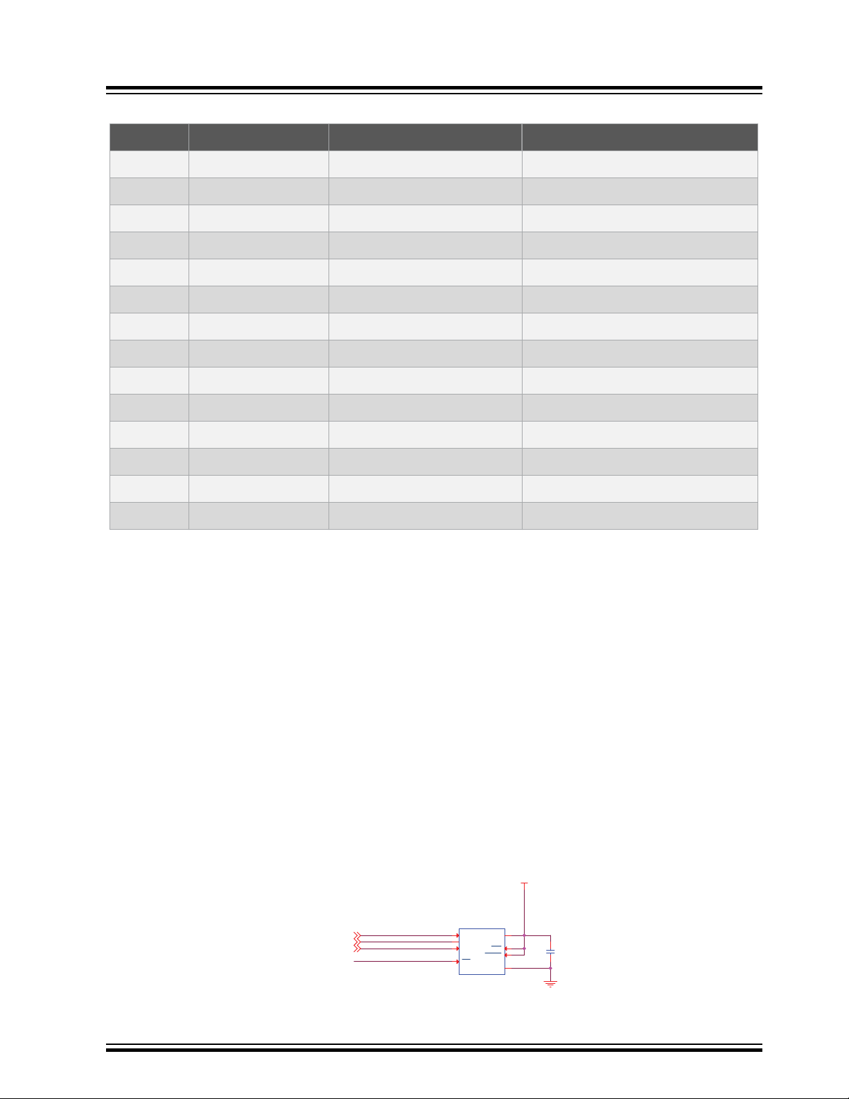
3.2.8.1 Serial Flash
The SAMA5D2 includes two high-speed Serial Peripheral Interface (SPI) controllers. The SPI is a full
duplex synchronous bus supporting a single master and multiple slave devices. The SPI bus consists of
the following items:
•
a serial clock line (generated by the master)
•
a data output line from the master
• a data input line to the master
• one or more active low chip select signals (output from the master)
One SPI port is used to interface with the on-board serial Flash.
The following figure illustrates the implementation of an SPI Flash memory.
Figure 3-17. Serial Flash
© 2017 Microchip Technology Inc.
DS50002709A-page
18
Page 19
Note: The serial Flash is optional and not mounted on board.
QSPI0_CS_PA23
VDD_3V3
GND_POWER
VDD_3V3
VDD_3V3
QSPI0_IO0_PA24
QSPI0_IO1_PA25
QSPI0_IO2_PA26
QSPI0_IO3_PA27 QSPI0_SCK_PA22
U14
SST26VF064B-104I/SM
soic8jg
SI/SIO0
5
SO/SIO1
2
SIO2
3
SIO37SCLK
6
CS#
1
GND
4
VCC
8
C120
100nF
C0402
R186
10K
R0402
R187
10K
R0402
JP13
Header 1X2
1
2
R242
10K
3.2.8.2 QSPI Serial Flash
The SAMA5D2 provides two Quad Serial Peripheral Interfaces (QSPI).
A QSPI is a synchronous serial data link that provides communication with external devices in Master
mode.
The QSPI can be used in SPI mode to interface with serial peripherals (such as ADCs, DACs, LCD
controllers, CAN controllers and sensors), or in Serial Memory mode to interface with serial Flash
memories.
The QSPI allows the system to execute code directly from a serial Flash memory (XIP, or Execute In
place, technology) without code shadowing to RAM. The serial Flash memory mapping is seen in the
system as other memories (ROM, SRAM, DRAM, etc.).
With the support of the Quad SPI protocol, the QSPI allows the system to use high-performance serial
Flash memories which are small and inexpensive, instead of larger and more expensive parallel Flash
memories.
The figure below illustrates the implementation of a QSPI Flash memory.
Figure 3-18. QSPI Serial Flash
SAMA5D2-PTC-EK
Board Components
A jumper (JP13) is used to disable the QSPI Flash.
Table 3-5. SPI and QSPI Signal Descriptions
PIO Mnemonic PIO Shared Signal Description
PA14 SPI0_SPCK _ SPI clock
PA15 SPI0_MOSI _ Master out - Slave in
PA16 SPI0_MISO _ Master in - Slave out
PA17 SPI0_NPCS0 _ Chip select
_ _ _ _
PA22 QSPI0_SCK SDMMC1-Nand Flash QSPI clock
PA23 QSPI0_CS Nand Flash Chip select
PA24 QSPI0_IO0 Nand Flash Data0
PA25 QSPI0_IO1 Nand Flash Data1
© 2017 Microchip Technology Inc.
DS50002709A-page
19
Page 20
PIO Mnemonic PIO Shared Signal Description
BOOT_DIS
QSPI Flash CS
SPI Flash CS
QSPI0_CS_PA23
SPI0_CS0_PA17
GND_POWER
GND_POWER
VDD_3V3
SPI0_NPCS0_PA17
QSPI0_NPCS_PA23
DISABLE_BOOT
C116
100nF
VCC
GND
U11
NL17SZ126DFT2G
1
2
3
4
5
VCC
GND
U12
NL17SZ126DFT2G
1
2
3
4
5
R184
10K
C117
100nF
R185
10K
R178
10K
CAUTION
PA26 QSPI0_IO2 Nand Flash Data2
PA27 QSPI0_IO3 Nand Flash Data3
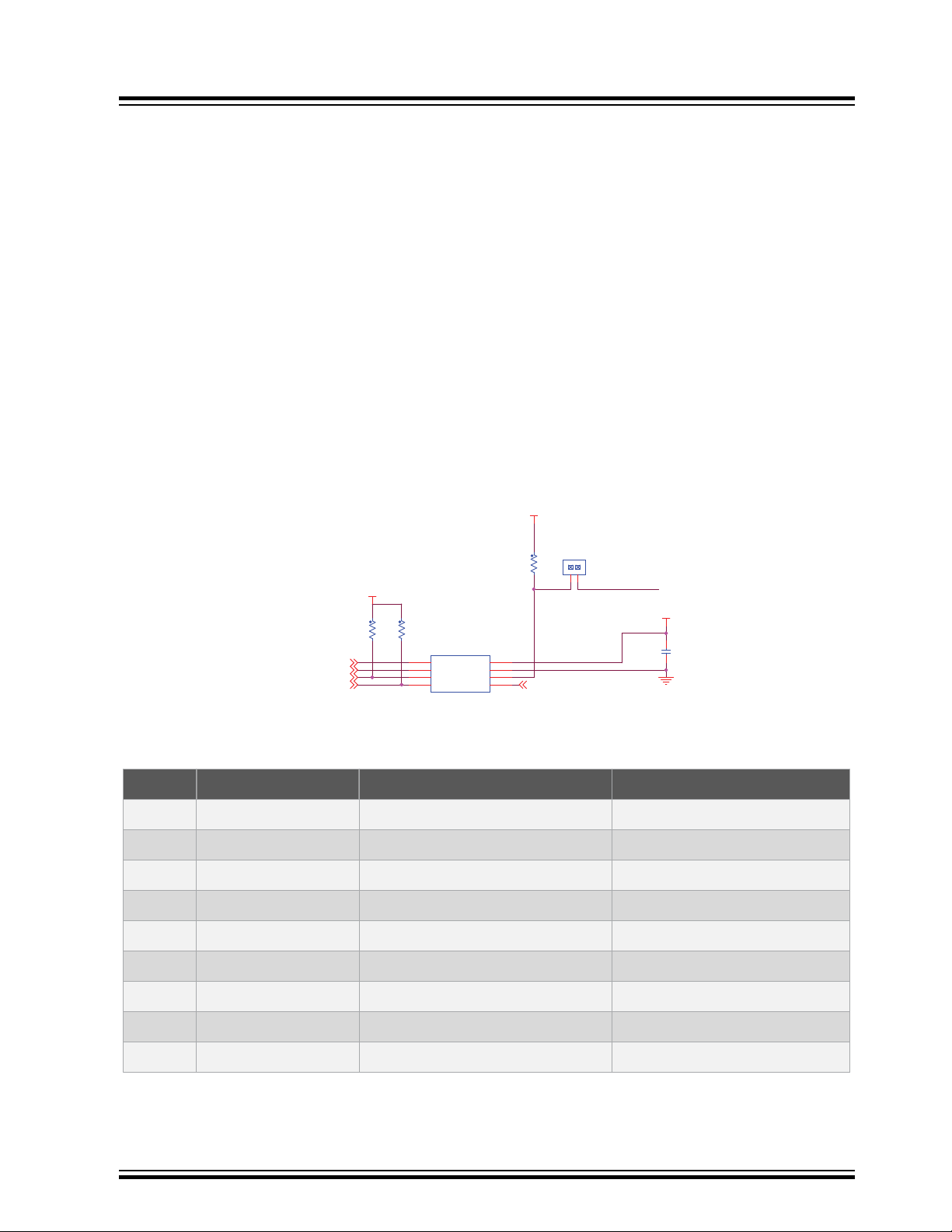
3.2.8.3 CS Disable
On-board push button PB2 controls the selection (CS#) of the bootable memory components (QSPI and
serial Flash) using a non-inverting 3-state buffer
Figure 3-19. CS Disable
SAMA5D2-PTC-EK
Board Components
.
3.2.8.4
The rule of operation is:
• PB2 (DISABLE_BOOT) and PB3 (RESET) pressed = booting from QSPI or optional serial Flash is
disabled.
Refer to the SAMA5D2 Series datasheet for more information on standard boot strategies and
sequencing.
Serial EEPROM with Unique MAC Address
The SAMA5D2-PTC-EK board embeds one Microchip 24AA02E48 I²C serial EEPROM connected on the
TWI1 interface.
The TWI interface is I2C-compatible and similarly uses only two lines, namely serial data (SDA) and serial
clock (SCL). According to the standard, the TWI clock rate is limited to 400 kHz in Fast mode and 100
kHz in Normal mode, but configurable baud rate generator permits the output data rate to be adapted to a
wide range of core clock frequencies. The TWI is used in Master mode.
The 24AA02E48 features 2048 bits of Serial Electrically-Erasable Programmable Read-Only Memory
(EEPROM) organized as 256 words of eight bits each and is accessed via an I2C-compatible (2-wire)
serial interface. In addition, the 24AA02E48 incorporates an easy and inexpensive method to obtain a
globally unique MAC or EUI address (EUI-48).
The EUI-48 addresses can be assigned as the actual physical address of a system hardware device or
node, or it can be assigned to a software instance. These addresses are factory-programmed by
Microchip and guaranteed unique. They are permanently write-protected in an extended memory block
located outside the standard 2-Kbit memory array.
Caution: The EEPROM device is used as a “software label” to store board information such as
chip type, manufacturer name and production date, using the last two 16-byte blocks in
memory. The information contained in these blocks should not be modified.
© 2017 Microchip Technology Inc.
DS50002709A-page
20
Page 21

Table 3-6. EEPROM PIOs Signal Descriptions
TWD1
TWCK1
GND_POWER
VDD_3V3
GND_POWER
TWD1_PC6
TWCK1_PC7
C118
100nF
C0402
R188
10K
R0402
U15
24AA02E48
8MA2
A0
1
A1
2
A2
3
GND
4
SDA
5
SCL
6
WP
7
VCC
8
(MCI0_C D)
(MCI0_WP)
(MCI0_DA1)
(MCI0_DA0)
(MCI0_CK)
(MCI0_CD A)
(MCI0_DA3)
(MCI0_DA2)
(MCI0_DA4)
(MCI0_DA5)
(MCI0_DA7)
(MCI0_DA6)
GND_POWER
GND_POWER
VDDSDHC
VDD_3V3
SDMMC0_CK_PA0
SDMMC0_CMD_PA1
SDMMC0_DAT1_PA3
SDMMC0_DAT2_PA4
SDMMC0_DAT3_PA5
SDMMC0_DAT4_PA6
SDMMC0_DAT5_PA7
SDMMC0_DAT6_PA8
SDMMC0_DAT7_PA9
SDMMC0_WP_PA12
SDMMC0_CD_PA13
SDMMC0_DAT0_PA2
R154
0R
R0402
R169
10k
R0402
R167
68k
R0603
R173
10k
R0402
C110 10uF
C0603
R161
68k
R0603
R155
68k
R0603
R163
68k
R0603
J6
7SDMM-B0-2211
con_kingconn_7sdmm_2211
8
5
7
6
4
3
2
1
9
14
15
16
13
12
11
10
R165
68k
R0603
R171
0R
R0402
R157
68k
R0603
R172
10k
R0402
C111 100nF
C0402
R158
68k
R0603
R159
68k
R0603
PIO Mnemonic Shared Signal Description
PC6 TWD1 XPRO TWI Data
PC7 TWCL1 XPRO TWI Clock
The figure below illustrates the implementation for the EEPROM.
Figure 3-20. EEPROM 24AA02E48
3.2.9 Secure Digital Multimedia Card (SDMMC) Interface
The SD (Secure Digital) Card is a non-volatile memory card format used as a mass storage memory in
mobile devices.
SAMA5D2-PTC-EK
Board Components
3.2.9.1 Secure Digital Multimedia Card (SDMMC) Controller
The SAMA5D2-PTC-EK board has two Secure Digital Multimedia Card (SDMMC) interfaces that support
the MultiMedia Card (e.MMC) Specification V4.41, the SD Memory Card Specification V3.0, and the
SDIO V3.0 specification. It is compliant with the SD Host Controller Standard V3.0 Specification.
•
The SDMMC0 interface is connected to a standard SD card interface.
The SDMMC1 interface is connected to a microSD card interface.
•
3.2.9.2 SDMMC0 Card Connector
A standard MMC/SD card connector, connected to SDMMC0, is mounted on the top side of the board.
The SDMMC0 communication is based on a 12-pin interface (clock, command, data (8) and power lines
(2)). A card detection switch is included.
The figure below illustrates the implementation for the SDMMC0 interface.
Figure 3-21. SDMMC0 Standard SD Socket
© 2017 Microchip Technology Inc.
DS50002709A-page
21
Page 22

Figure 3-22. Standard SD Socket J6 Location
SAMA5D2-PTC-EK
Board Components
The table below describes the pin assignment of SD/MMC connector J6.
Table 3-7. Standard SD Socket J6 Pin Assignment
Pin No Mnemonic Signal Description
1 MCI0_DA3 SDMMC0_DAT3_PA5
2 MCI0_CDA SDMMC0_CMD_PA1
3 GND GND
4 VCC VDDSDHC (3.3V or 1.8V)
5 MCI0_CK SDMMC0_CK_PA0
6 MCI0_CD SDMMC0_CD_PA13 (card detect)
7 MCI0_DA0 SDMMC0_DAT0_PA2
8 MCI0_DA1 SDMMC0_DAT1_PA3
9 MCI0_DA2 SDMMC0_DAT2_PA4
10 MCI0_DA4 SDMMC0_DAT4_PA6
11 MCI0_DA5 SDMMC0_DAT5_PA7
12 MCI0_DA6 SDMMC0_DAT6_PA8
13 MCI0_DA7 SDMMC0_DAT7_PA9
© 2017 Microchip Technology Inc.
DS50002709A-page
22
Page 23

Pin No Mnemonic Signal Description
GND_POWER
GND_POWER
VDD_3V3
VDD_3V3
VDDSDHC1V8
VDDSDHC
SDMMC0_VDDSEL_PA11
U9
ADG849YKSZ-REEL
SC70
S2
6
S1
4
IN
1
GND
3
D
5
VDD
2
R151 DNP
R0402
R150
10k
R0402
R152 DNP
R0402
C107
100nF
C0402
(MCI1_DA1)
(MCI1_DA0)
(MCI1_CK)
(MCI1_CD A)
(MCI1_DA3)
(MCI1_DA2)
(MCI1_C D)
GND_POWER
GND_POWER
VDD_3V3
SDMMC1_CK_PA22
SDMMC1_CD_PA30
SDMMC1_CMD_PA28
SDMMC1_DAT1_PA19
SDMMC1_DAT0_PA18
SDMMC1_DAT2_PA20
SDMMC1_DAT3_PA21
R160
10k
R0402
R162
68k
R0603
R170
10k
R0402
R164
68k
R0603
R166
68k
R0603
R168
68k
R0603
C109
100nF
C0402
C108
10uF
C0603
SW1
SW2
J7
PJS008-2120-0
Micro_SD_PJS008
8
5
7
6
4
3
2
1
9
13
12
11
10
14
14 MCI0_WP SDMMC0_WP_PA12
15 GND GND
16 GND GND
3.2.9.3 SDMMC0 VDDHC Voltage Switching
The board uses an ADG849 to switch the power line VDDSDHC_3V3 or VDDSDHC_1V8 through the
command line SDMMC0_VDDSEL_PA1
Figure 3-23. SDMMC0 VDDSDHC Voltage Switching
SAMA5D2-PTC-EK
Board Components
1.
Table 3-8. SDMMC1 Power Command
PIO Mnemonic Signal Description
PA11 SDMMC0_VDDSEL Selects 3.3V or 1.8V
3.2.9.4 SDMMC1 Card Connector
A microSD card connector, connected to SDMMC1, is mounted on the top side of the board. The
SDMMC1 communication is based on a 9-pin interface (clock, command, card detect, four data and
power lines). A card detection switch is included. The microSD connector can be used to connect any
microSD card for mass storage.
Figure 3-24. SDMMC1 microSD Socket
© 2017 Microchip Technology Inc.
DS50002709A-page
23
Page 24

Figure 3-25. microSD Socket J7 Location
SAMA5D2-PTC-EK
Board Components
The table below describes the pin assignment of microSD connector J7.
Table 3-9. microSD Socket J7 Pin Assignment
Pin No Mnemonic PIO Shared Signal Description
1 SDMMC1_DAT2 PA20 – Data bit 2
2 SDMMC1_DAT3 PA21 – Data bit 3
3 SDMMC1_CDA PA28 – Command
4 VCC – – 3.3V supply voltage
5 SDMMC1_CK PA22 – Clock
6 GND – – Common ground
7 SDMMC1_DAT0 PA18 – Data bit 0
8 SDMMC1_DAT1 PA19 – Data bit 1
9 SW1 GND – Not used
10 SDMMC1_CD PA30 – Card detection switch
11 GND – – Common ground
© 2017 Microchip Technology Inc.
DS50002709A-page
24
Page 25

Pin No Mnemonic PIO Shared Signal Description
top/bo t
top/bo t
top/bo t
top/bo t
ETH_LED0
TX+
ETH_XI
ETH_XO
ETH_LED1
TX-
RX+
RX-
GND_POWER
GND_POWER
GND_POWER
GND_POWER
VDDA_3V3
VDD_3V3
VDD_3V3
VDD_3V3
ETH_INT_PB24
ETH_GTXCK_PB14
ETH_GTXEN_PB15
ETH_GRXDV_PB16
ETH_GRXER_PB17
ETH_GRX0_PB18
ETH_GRX1_PB19
ETH_GTX0_PB20
ETH_GTX1_PB21
ETH_GMDC_PB22
ETH_GMDIO_PB23
NRST
R200
10K
R0402
R198
1K
R0402
R202
10K
R0402
U17
KSZ8081RNB
qfn32_1p5h
RXC/B-CAST_OFF
19
CRS/CONFIG1
29
COL/CONFIG0
28
TXD1
25
TXD0
24
TXEN
23
RXD3/PHYAD0
13
RXD2/PHYAD1
14
RXD1/PHYAD2
15
RXD0/DUPLEX
16
RXDV/CONFIG2
18
RXER/ISO
20
MDC
12
MDIO
11
INTRP/NAND
21
VDDA_3V3
3
VDDIO
17
RESET
32
TXP
7
TXM
6
RXP
5
RXM
4
VDD_1V2
2
GND
1
PADDLE
33
TXC
22
TXD2
26
TXD3
27
REXT
10
XO
8
XI
9
LED0/NWAYEN
30
LED1/SPEED
31
R193
10K
R0402
R197
1K
R0402
C130
100nF
C0402
R192
10K
R0402
C128
10uF
C0603
R199
10K
R0402
C129
100nF
C0402
R203
10K
R0402
R204
10K
R0402
C123 2.2uF
C0603
C127
10uF
C0603
C124 100nF
C0402
R205
10K
R0402
L19
BLM18PG181SN1D
R0603
1 2
R206
10K
R0402
R194 6.49K 1%
R0402
R196 0R
R0402
R201
10K
R0402
12 GND – – Common ground
13 GND – – Common ground
14 GND – – Common ground
3.2.10 Communication Interfaces
The SAMA5D2-PTC-EK board is equipped with Ethernet and USB host/device communication interfaces.
This section describes the signals and connectors related to the ETH and USB communication interfaces.
3.2.10.1 Ethernet 10/100 (GMAC) Port
The SAMA5D2-PTC-EK board features a Micrel PHY device (KSZ8081) operating at 10/100 Mb/s. The
board supports RMII interface modes. The Ethernet interface consists of two pairs of low-voltage
differential pair signals designated from GRX± and GTX± plus control signals for link activity indicators.
These signals can be used to connect to a 10/100 Base-T RJ45 connector integrated on the SAMA5D2PTC-EK board.
An individual 48-bit MAC address (Ethernet hardware address) is allocated to each product. This number
is stored in the Microchip 24AA02E48 I2C serial EEPROM (refer to Serial EEPROM with Unique MAC
Address).
SAMA5D2-PTC-EK
Board Components
Additionally
, for monitoring and control purposes, a LED functionality is carried on the RJ45 connectors to
indicate activity, link, and speed status.
For more information about the Ethernet controller device, refer to the Micrel KSZ8081RN controller
manufacturer's datasheet.
Figure 3-26. Ethernet Interface
© 2017 Microchip Technology Inc.
DS50002709A-page
25
Page 26

LINK
ACT
ETH_LED0
TX+
ETH_LED1
RX-
RX+
TX-
EARTH_ETH
EARTH_ETH
GND_ETH
VDD_3V3
R190 510R
R0402
C122
100nF
C0402
C121
100nF
C0402
1
2
3
6
4
5
7
8
75
75
75 75
1nF
TD+
TD-
CT
NC
RD-
CT
TX+
TX-
RX+
RX-
RD+
Left Green LED
Right yellow LED
J8 13F-64GYD2PL2NL
rj45_13f-64gy_P12_4
1
2
7
8
3
6
5
4
9
10
11
12
13
14
15
16
R189 510R
R0402
SAMA5D2-PTC-EK
Table 3-10. Ethernet PHY 10/100 Signal Descriptions
PIO Mnemonic Shared Signal Description
PB14 ETH_GTXCK _ Transmit clock
PB15 ETH_GTXEN _ Transmit enable
PB16 ETH_GRXDV _ Receive data valid
PB17 ETH_GRXER _ Receive error
PB18 ETH_GRX0 _ Receive data 0
PB19 ETH_GRX1 _ Receive data 1
PB20 ETH_GTX0 _ Transmit data 0
PB21 ETH_GTX1 _ Transmit data 1
PB22 ETH_GMDC _ Management data clock
PB23 ETH_GMDIO _ Management data in/out
PB24 ETH_GTX_INT _ Interrupt (open drain)
Board Components
Figure 3-27. Ethernet PHY Connector J8
© 2017 Microchip Technology Inc.
DS50002709A-page
26
Page 27

Figure 3-28. Ethernet RJ45 Connector J8 Location
SAMA5D2-PTC-EK
Board Components
The table below describes the pin assignment of Ethernet connector J8.
Table 3-1
1. Ethernet RJ45 Connector J8 Pin Assignment
Pin No Mnemonic Signal Description
1 TX+ Transmit
2 TX- Transmit
3 RX+ Receive
4 Decoupling capacitor –
5 Decoupling capacitor –
6 RX- Receive
7 NC –
8 EARTH / GND Common ground
9 ACT LED LED activity
10 ACT LED LED activity
11 LINK LED LED link connection
12 LINK LED LED link connection
13 EARTH / GND Common ground
© 2017 Microchip Technology Inc.
DS50002709A-page
27
Page 28

Pin No Mnemonic Signal Description
14 EARTH / GND Common ground
15 NC –
16 NC –
3.2.10.2 USB Host/Device A, B
The USB (Universal Serial Bus) is a hot-pluggable general-purpose high-speed I/O standard for computer
peripherals. The standard defines connector types, cabling, and communication protocols for
interconnecting a wide variety of electronic devices. The USB 2.0 Specification defines data transfer rates
as high as 480 Mbps (also known as High Speed USB). A USB host bus connector uses 4 pins: a power
supply pin (5V), a differential pair (D+ and D- pins) and a ground pin.
The SAMA5D2-PTC-EK board features three USB communication ports named USB-A to USB-C:
•
USB-A device interface
– One USB device standard micro-AB connector.
– This port has a VBUS detection function made through the R148-R149 resistor bridge.
– The USB-A port is used as a primary power source and as a communication link for the
board, and derives power from the PC over the USB cable. In most cases, this port is limited
to 500 mA.
• USB-B (host port B high- and full-speed interface)
– One USB host type A connector.
– The USB-B host port is equipped with a 500 mA high-side power switch to enable powering
devices connected to it.
• UBC-C (High-Speed Inter-Chip/HSIC port)
– One USB high-speed host port with an HSIC interface.
– The port is connected to a single 2-pin jumper.
SAMA5D2-PTC-EK
Board Components
3.2.10.3 USB-A Interface
© 2017 Microchip Technology Inc.
DS50002709A-page
28
Page 29

Figure 3-29. USB-A Type microAB Connector J4 Location
GND_POWER
EARTH_USB_A
GND_POWER
GND_POWER
VBUS_USBA
USBA_VBUS_5V_PB11
USBA_DP
USBA_DM
C103
20pF
C0402
VBUS
SHD
DM
DP
ID
GND
J4
MicroUSB AB Connector
USBMICRO5_6A
1
2
3
4
5
8
6
11
7
9
10
R149
200K
R0402
R148 100K
R0402
SAMA5D2-PTC-EK
Board Components
3.2.10.4 USB-A VBUS Detection
The USB-A port (J4) features a VBUS detection function provided by the R148-R149 resistor bridge.
The figure below shows the USB implementation on the USBA port.
Figure 3-30. USB-A Power and VBUS Detection
Table 3-12. USB-A PIO Signal Descriptions
PIO Mnemonic Shared Signal Description
PB11 USBA_VBUS_5V - VBUS insertion detection
3.2.10.5 USB-B Interface
The figure below shows the USB implementation on the USB-B port.
© 2017 Microchip Technology Inc.
DS50002709A-page
29
Page 30

Figure 3-31. USB-B Interface
USBB_VBUS_5V
GND_POWER
EARTH_USB_B
USBB_DP
USBB_DM
A
J3
Single USB Type A
USB4_2AL
VBUS
1
DM
2
DP
3
GND
4
SH1
5
SH2
6
Figure 3-32. USB-B Type A Connector J3 Location
SAMA5D2-PTC-EK
Board Components
Table 3-13. USB-B PIO Signal Descriptions
PIO Mnemonic Shared Signal Description
PB12 USBB_EN_5V – Power switch enable (active high)
PB13 USBB_OVCUR – Indicates overcurrent (open drain)
USB-B Power Switch
The USB-B Host port is equipped with a 500 mA high-side power switch for self-powered and buspowered applications. If the client device is bus-powered, the carrier can supply a 5V, 500mA power to
the client device. The USBB_EN_5V_PB12 signal controls the power switch and current limiter, the Micrel
MIC2025, which in turn supplies power to a bus-powered client device. Per the USB specification, buspowered USB 2.0 devices are limited to a maximum of 500 mA. The MIC2025 limits the current and
indicates an overcurrent with the USBB_OVCUR_PB13 signal.
© 2017 Microchip Technology Inc.
DS50002709A-page
30
Page 31

The table below describes the pin assignment of the USB-A and USB-B connectors.
HSIC_DATA
HSIC_STRB
J5
DNP
1
2
Table 3-14. USB-A and USB-B Connector Signal Descriptions
3.2.10.6 HSIC
High-Speed Inter-Chip (HSIC) is a standard for USB chip-to-chip interconnect with a 2-signal (strobe,
data) source synchronous serial interface using 240 MHz DDR signaling to provide only high-speed 480
Mbps data rate.
The interface operates at high speed, 480 Mbps, and is fully compatible with existing USB software
stacks. It meets all data transfer needs through a single unified USB software stack.
SAMA5D2-PTC-EK
Board Components
Pin No Mnemonic Signal Description
1 VBUS 5V power
2 DM Data minus
3 DP Data plus
4 ID On-the-go identification
5 GND Common ground
The HSIC interface is not used on the board and is connected to two-point jumper J5 (not mounted).
Figure 3-33. HSIC Interface
3.3 External Interfaces
3.3.1 LCD TFT Interface
This section describes the signals and connectors related to the LCD interface.
3.3.1.1 LCD Interface
The SAMA5D2-PTC-EK board provides a connector with 18 bits of data and control signals to the LCD
interface. Other signals are used to control the LCD and are available on connector J16: TWI, SPI, two
GPIOs for interrupt, 1-wire and power supply lines.
This connector is used to connect LCD display series 43xx or 70xx from PDA.
3.3.1.2 LCD Expansion Header
J16 is a 1.27-mm pitch, 50-pin header. It gives access to the LCD signals.
© 2017 Microchip Technology Inc.
DS50002709A-page
31
Page 32

Figure 3-34. LCD Expansion Header Interface
GND_POWER
VDD_3V3VDD_MAIN_5V
LCD_D2_PC10
LCD_D3_PC11
LCD_D4_PC12
LCD_D5_PC13
LCD_D6_PC14
LCD_D7_PC15
LCD_D10_PC16
LCD_D11_PC17
LCD_D12_PC18
LCD_D13_PC19
LCD_D14_PC20
LCD_D15_PC21
LCD_D18_PC22
LCD_D19_PC23
LCD_D20_PC24
LCD_D21_PC25
LCD_D22_PC26
LCD_D23_PC27
LCD_PCLK_PD0
LCD_VSYNC_PC30
LCD_HSYNC_PC31
LCD_DE_PD1
LCD_EN_PC29
LCD_IRQ1_PC9
LCD_IRQ2_PD2
LCD_PWM_PC28
SPI_CS_PB31
SPI_SCK_PB30
SPI_MISO_PB29
SPI_MOSI_PB28
TWI_SCL_PB29
TWI_SDA_PB28
NRST
SPI_CS_PB31
R230
DNP
R0603
R231
0R
R0603
R234
100R-1%
R0402
J16
XF2M-5015-1A
FPC50-0p5mm
ID
1
GND1
2
D0
3
D1
4
D2
5
D3
6
GND2
7
D4
8
D5
9
D6
10
D7
11
GND3
12
D8
13
D9
14
D10
15
D11
16
GND4
17
D12
18
D13
19
D14
20
D15
21
GND5
22
D16
23
D17
24
D18
25
D19
26
GND6
27
D20
28
D21
29
D22
30
D23
31
GND7
32
PCLK/CMD
33
VSYNC/CS
34
HSYNC/WE
35
DE/RE
36
SPI_SCK
37
SPI_MOSI
38
SPI_MISO
39
SPI_CS
40
ENABLE
41
TWI_SDA
42
TWI_SCL
43
IRQ1
44
IRQ2
45
PWM
46
RESET
47
VCC1
48
VCC2
49
GND8
50
SAMA5D2-PTC-EK
Board Components
3.3.1.3 LCD Power
In order to operate correctly with various LCD modules, two voltage lines are available: 3.3V and 5VCC
(default). The selection is made with 0R resistors R230 and R231.
© 2017 Microchip Technology Inc.
DS50002709A-page
32
Page 33

3.3.1.4 LCD Connector JX
Figure 3-35. LCD Connector J16 Location
SAMA5D2-PTC-EK
Board Components
The table below describes the pin assignment of LCD FPC connector J16.
able 3-15. LCD Connector J16 Signal Descriptions
T
Pin No Signal PIO Signal RGB Interface Function
1 ID PB31 _ ID LCD module
2 GND _ GND GND
3 LCDDAT0 – D0 –
4 LCDDAT1 – D1 –
5 LCDDAT2 PC10 D2 Data line
6 LCDDAT3 PC11 D3 Data line
7 GND _ GND GND
8 LCDDAT4 PC12 D4 Data line
9 LCDDAT5 PC13 D5 Data line
10 LCDDAT6 PC14 D6 Data line
© 2017 Microchip Technology Inc.
DS50002709A-page
33
Page 34

SAMA5D2-PTC-EK
Board Components
Pin No Signal PIO Signal RGB Interface Function
11 LCDDAT7 PC15 D7 Data line
12 GND _ GND GND
13 LCDDAT8 – D8 –
14 LCDDAT9 – D9 –
15 LCDDAT10 PC16 D10 Data line
16 LCDDAT11 PC17 D11 Data line
17 GND GND GND GND
18 LCDDAT12 PC18 D12 Data line
19 LCDDAT13 PC19 D13 Data line
20 LCDDAT14 PC20 D14 Data line
21 LCDDAT15 PC21 D15 Data line
22 GND _ GND GND
23 LCDDAT16 – D16 –
24 LCDDAT17 – D17 –
25 LCDDAT18 PC22 D18 Data line
26 LCDDAT19 PC23 D19 Data line
27 GND _ GND GND
28 LCDDAT20 PC24 D20 Data line
29 LCDDAT21 PC25 D21 Data line
30 LCDDAT22 PC26 D22 Data line
31 LCDDAT23 PC27 D23 Data line
32 GND _ GND GND
33 LCDPCK PD0 PCLK Pixel clock
34 LCDVSYNC PC30 VSYNC/CS Vertical sync
35 LCDHSYNC PC31 HSYNC/WE Horizontal sync
36 LCDDEN PD1 DATA_ENABLE Data enable
37 SPI_SPCK PB30 SPI_SCK –
38 SPI_MOSI PB28 SPI_MOSI (Shared with TWI)
39 SPI_MISO PB29 SPI_MISO (Shared with TWI)
40 SPI_NPCS0 PB31 SPI_CS –
41 LCDDISP PC29 ENABLE Display enable signal
42 TWD PB28 TWI_SDA I2C data line (maXTouch)
© 2017 Microchip Technology Inc.
DS50002709A-page
34
Page 35

Pin No Signal PIO Signal RGB Interface Function
LED
VDD_3V3
GND_POWER
GND_POWER
GND_POWER
GND_POWER
GND_POWER
LED_RED_PB10
LED_GREEN_PB8
LED_BLUE_PB6
R240 1K
R0402
R182 100R-1%
R0402
R183 100R-1%
R0402
R244
10K
Q7
BSS138
SOT23_123
1
3
2
R181 100R-1%
R0402
D4
CLV1A-FKB-CJ1M1F1BB7R4S3
Red
1
Green
4
Blue
3
Anode
2
R241 1K
R0402
R239 2.2K-1%
R0402
Q5
BSS138
SOT23_123
1
3
2
R243
10K
Q6
BSS138
SOT23_123
1
3
2
43 TWCK PB29 TWI_SCL I2C clock line (maXTouch)
44 GPIO PC9 IRQ1 maXTouch interrupt line
45 GPIO PD2 IRQ2 Interrupt line for other I2C devices
46 LCDPWM PC28 PWM Backlight control
47 RESET – RESET Reset for both display and maXTouch
48 Main_5V/3V3 VCC VCC 3.3V or 5V supply (0R)
49 Main_5V/3V3 VCC VCC 3.3V or 5V supply (0R)
50 GND _ GND GND
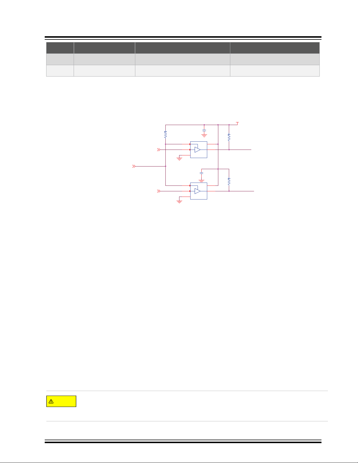
3.3.2 RGB LED
The SAMA5D2-PTC-EK board features one RGB LED which can be controlled by the user. The three
LED cathodes are controlled via GPIO PWM or timer/counter pins.
Figure 3-36. RGB LED Indicators
SAMA5D2-PTC-EK
Board Components
Table 3-16. RGB LED PIOS
3.4 Debugging Capabilities
The SAMA5D2-PTC-EK includes two main debugging interfaces to provide debug-level access to the
SAMA5D2:
• One UAR
• Two JTAG interfaces, one connected directly to the MPU using connector J2 and one through the
© 2017 Microchip Technology Inc.
JLINK-OB interface USB port J9
Signal PIO Function
LED_RED PB10 TIOB3
LED_GREEN PB8 PWML3
LED_BLUE PB6 PWML2
T through USB JLINK-CDC
DS50002709A-page
35
Page 36

3.4.1 Debug JTAG
GND_POWER
VDD_3V3
VDD_3V3
GND_POWER
NRST
CON_JTAG_Pin2
CON_JTAG_Pin4
CON_JTAG_Pin6
CON_JTAG_Pin8RTCKIN
R140
100K
R0402
R236
10K
R0402
R142
100K
R0402
R143 100R-1% R0402
R141
100K
R0402
R138 DNP
R0402
J2
Header 2X5
FTSH-105-01-F-DV-P-TR
1
2
3
4
5
6
7
8
9
10
This section describes the signals and connectors related to the JTAG interface.
A 10-pin JTAG header is provided on the SAMA5D2-PTC-EK board to facilitate software development
and debugging using various JT
Figure 3-37. JTAG Interface
Figure 3-38. JTAG Connector J2 Location
SAMA5D2-PTC-EK
Board Components
AG emulators. The interface signals have a voltage level of 3.3V.
The table below describes the pin assignment of JTAG connector J2.
© 2017 Microchip Technology Inc.
DS50002709A-page
36
Page 37

SAMA5D2-PTC-EK
Board Components
Table 3-17. JTAG/ICE Connector J2 Pin Assignment
Pin No Mnemonic Signal Description
1 VTref. 3.3V power This is the target reference voltage (main 3.3V).
2 TMS TEST MODE SELECT JTAG mode set input into target CPU
3 GND Common ground
TCK TEST CLOCK - Output timing signal,
4
for synchronizing test logic and control
register access
5 GND Common ground
TDO JTAG TEST DATA OUTPUT - Serial
6
data input from the target
RTCK - Input return test clock signal from
7
the target
JTAG clock signal into target CPU
JTAG data output from target CPU
Some targets with a slow system clock must
synchronize the JTAG inputs to internal clocks. In
the present case, such synchronization is
unneeded and TCK is merely looped back into
R
TCK.
TDI TEST DATA INPUT - Serial data output
8
line, sampled on the rising edge of the TCK
signal
9 GND Common ground
10 nRST RESET Active-low reset signal. Target CPU reset signal.
3.4.2 Embedded Debugger (JLINK-OB) Interface
The SAMA5D2-PTC-EK includes a built-in SEGGER J-Link-On-Board device. The functionality is
implemented with an ATSAM3U4C microcontroller in an LFBGA100 package. The A
the functions of JTAG and a bridge USB/Serial debug port (CDC). One two-colored LED (D6) mounted
near the SAM3 chip (U20) shows the status of the J-Link-On-Board device.
J-Link-OB-ATSAM3U4C was designed in order to provide an efficient, low-cost, on-board alternative to
the standard J-Link.
The USB JLINK-OB port is used as a secondary power source and as a communication link for the
board, and derives power from the PC over the USB cable. This port is limited in most cases to 500 mA.
A single PC USB port is sufficient to power the board.
JTAG data input into target CPU
TSAM3U4C provides
© 2017 Microchip Technology Inc.
DS50002709A-page
37
Page 38

Figure 3-39. JLINK-OB Interface
EDBG_USB_DP
EDBG_USB_DM
ENSPI
ERASE_3U
TDI_3U
TDO_3U
TCK_3U
TMS_3U
NRST_3U
TRSTIN
TRSTOUT
TRESIN
TRESOUT
TDIIN
TMSIN
TCKOUT
TMSOUT
TDIOUT
TDOIN
TCKIN
ENSPI
TCKOUT
PA25_3U
PA26_3U
LED2_3U
LED1_3U
EDBG_XIN
RX_3U
TX_3U
EARTH_USB_EDBG
VDD_3V3_3U
VDD_OUT_3U
VDD_3V3_3U
GND_POWER
VDD_3V3_3U
VDD_3V3_3U
GND_POWER
GND_POWER
VDD_3V3_3U
GND_POWER
VDD_3V3_3U
VBUS_JLINK
VDD_3V3_3U
GND_POWER
RTCKIN
R210
100R-1%
R0402
R211 39R R0402
R209
100R-1%
R0402
R215
100K
R0402
VBUS
SHD
DM
DP
ID
GND
J9
MicroUSB AB Connector
USBMICRO5_6A
1
2
3
4
5
8
6
11
7
9
10
R212 39R R0402
C156
100nF
C0402
R208
10K
R0402
R245
0R
R214
6.8K-1%
R0402
C136 10nF
C0402
D5 PMEG6010CEGWX
sod123
Y4
ASE-12.000MHz-LC-T
NC
1
VCC4Out
3
GND
2
U20
ATSAM3U4CA-CU
TFBGA100
VBG
A1
XIN
A2
XOUT
A3
PB17
A4
PB21A5PB23
A6
TCK/SWCLK
A7
VDDIN
A8
VDDOUT
A9
XIN32
A10
VDDCORE_1
B1
GNDUTMI
B2
VDDUTMI
B3
PB10
B4
PB18
B5
PB24
B6
NRST
B7
TDO/TRACESWO
B8
TDI
B9
XOUT32
B10
DFSDP
C1
DHSDP
C2
GNDPLL
C3
PB14
C4
PB19
C5
PB22
C6
TMS/SWDIO
C7
NRSTB
C8
JTAGSEL
C9
VDDBU
C10
DFSDM
D1
DHSDM
D2
VDDPLL
D3
VDDCORE_2
D4
PB20
D5
ERASE
D6
TST
D7
FWUP
D8
PA11/PGMD3
D9
PA12/PGMD4
D10
PA29
E1
GND_1
E2
PA28
E3
PB9
E4
GNDBU
E5
VDDIO_3
E6
VDDCORE_3
E7
PA10/PGMD2
E8
PA9/PGMD1
E9
PA8/PGMD0
E10
PB1
F1
PB12
F2
VDDIO_1
F3
PA31
F4
VDDIO_2
F5
GND_2
F6
PB16
F7
PA6/PGMM2
F8
VDDCORE_6
F9
PA7/PGMM3
F10
PB11
G1
PB2G2PB0
G3
PB13
G4
VDDCORE_5
G5
GND_3
G6
PB15
G7
PA3/PGMNVALID
G8
PA5/PGMM1
G9
PA4/PGMM0
G10
VDDCORE_4
H1
PB5
H2
PA27
H3
PA22/PGMD14
H4
PA13/PGMD5
H5
PA15/PGMD7
H6
PA18/PGMD10
H7
PA24
H8
PA1/PGMRDY
H9
PA2/PGMNOE
H10
PB6J1PB8
J2
ADVREF
J3
PA30
J4
PB3
J5
PA16/PGMD8
J6
PA19/PGMD11
J7
PA21/PGMD13
J8
PA26
J9
PA0/PGMNCMD
J10
PB7
K1
VDDANA
K2
GNDANA
K3
AD12BVREF
K4
PB4
K5
PA14/PGMD6
K6
PA17/PGMD9
K7
PA20/PGMD12
K8
PA23/PGMD15
K9
PA25
K10
C137 10pF
C0402
C132 10nF
C0402
R213
DNP
R0402
VDD_3V3_3U
R216 150R-1%
R0402
R217 150R-1%
R0402
D6
KPTB-1615
Green
4
1
1
RED
2
3
3
LED1_3U
LED2_3U
ERASE_3U
VDD_3V3_3U
JP11
Header 1X2
1
2
JTAG-OB disable
JTAG-CDC disable
PA25_3U
PA26_3U
VDD_3V3_3U
GND_POWER
GND_POWER
VDD_3V3_3U
JP9
Header 1X2
1
2
R224
10K
R0402
R225
10K
R0402
JP10
Header 1X2
1
2
SAMA5D2-PTC-EK
Board Components
3.4.2.1 Disabling JLINK-OB (ATSAM3U4C)
Jumper JP10 disables the J-Link-OB-ATSAM3U4C JTAG functionality. When the jumper is installed, it
grounds pin 26 of the ATSAM3U4C that is normally pulled high. A quad analog switch is used to select
AG interface.
the JT
• Jumper JP10 not installed: J-Link-OB-ATSAM3U4C is enabled and fully functional.
• Jumper JP10 installed: J-Link-OB-ATSAM3U4C is disabled and an external JTAG controller can be
used through the 10-pin JTAG port J2.
© 2017 Microchip Technology Inc.
Jumper JP10 disables only the J-Link functionality. The debug serial com port that is emulated through a
Communication Device Class (CDC) of the same USB connector remains operational (if JP9 is open).
Figure 3-40. Enabling/Disabling JLINK-OB and JLINK-CDC
DS50002709A-page
38
Page 39

Figure 3-41. JTAG Switch
TDIOUT
TDIIN
PA26_3U
PA26_3U
TDOIN
TMSIN
TMSOUT
TCKIN
TCKOUT
VDD_3V3_3U
GND_POWER
JTAG_TCK_PD27
JTAG_TMS_PD30
JTAG_TDI_PD28
CON_JTAG_Pin2
CON_JTAG_Pin4
CON_JTAG_Pin8
JTAG_TDO_PD29
CON_JTAG_Pin6
R223 150R-1%
R0402
U22
NLAS3899BMNTWG
WQFN-16
NCA
1
COMA
16
NOA
15
NOB
3
COMB
4
NCB
5
ABIN
2
NOC
7
COMC
8
NCC
9
CDIN
10
NOD
11
COMD
12
NCD
13
VCC
14
GND
6
R222 150R-1%
R0402
R218 150R-1%
R0402
3.4.3 Hardware UART via CDC
In addition to the J-Link-OB functionality, the ATSAM3U4C microcontroller provides a bridge to a debug
serial port (UART DBGU) of the SOM's processor
connection used by JTAG by implementing Communication Device Class (CDC), which allows terminal
communication with the target device.
SAMA5D2-PTC-EK
Board Components
. The port is made accessible over the same USB
This feature is enabled only if the SAM3U/PA25 (pin K10) is not grounded. The pin is normally pulled high
and controlled by jumper JP9.
• Jumper JP9 not installed: the J-Link-CDC is enabled and fully functional.
• Jumper JP9 installed: the J-Link-CDC device is disabled.
The USB Communications Device Class (CDC) enables to convert the USB device into a serial
communication device. The target device running USB-Device CDC is recognized by the host as a serial
interface (USB2COM, virtual COM port) without the need to install a special host driver (since the CDC is
standard). All PC software using a COM port work without modifications with this virtual COM port. Under
Windows, the device shows up as a COM port; under Linux, as a /dev/ACMx device. This enables the
user to use host software which was not designed to be used with USB, such as a terminal program.
Table 3-18. Debug COM Port PIOs Signal Descriptions
PIO Mnemonic Shared Signal Description
PB26 URXD0 - Receive data
PB27 UTXD0 - Transmit data
© 2017 Microchip Technology Inc.
DS50002709A-page
39
Page 40

Figure 3-42. JLINK-OB and CDC USB Connector J9 Location
SAMA5D2-PTC-EK
Board Components
The table below describes the pin assignment of USB connector J9.
Table 3-19. USB Connector J9 Pin Assignment
Pin No Mnemonic Signal Description
1 VBUS 5V power
2 DM Data minus
3 DP Data plus
4 ID Not used
5 GND Common ground
3.4.3.1 Board Edge Connector
This connector is used to upgrade or download code to the ATSAM3U4C microcontroller JLINK-OB.
3.5 PIO Usage on Expansion Connectors
3.5.1 PIOBU Interface
The SAMA5D2-PTC-EK board features eight tamper pins for static or dynamic intrusion detection, UART
reception, and two analog pins for comparison.
© 2017 Microchip Technology Inc.
DS50002709A-page
40
Page 41

RXD
PIOBU0
ACN
PIOBU2
PIOBU4
PIOBU6
PIOBU3
PIOBU5
ACP
GND_POWER
R132 0R R0402R127 330R R0402
R130 330R
R0402
R124 330R R0402 R129 330R R0402
R131 0R R0402
R125 330R
R0402
J1
DNP
FTSH-105-01-F-DV-P-TR
1
2
3 4
5
6
7 8
9
10
R126 330R R0402
R128 0R R0402
SAMA5D2-PTC-EK
Board Components
For a description of intrusion detection, refer to the SAMA5D2 datasheet, chapter "Security Module".
Figure 3-43. PIOBU Connector
Figure 3-44. PIOBU Connector J1 Location
The table below describes the pin assignment of PIOBU connector J1.
Table 3-20. PIOBU Connector J1 Pin Assignment
3.5.2 mikroBUS Interface
The SAMA5D2-PTC-EK hosts a pair of 8-pin female headers as mikroBus interface. The mikroBUS
interface defines the main board sockets and add-on boards used for interfacing microprocessors with
© 2017 Microchip Technology Inc.
Signal Pin No. Signal
PIOBU0 1 2 PIOBU3
PIOBU2 3 4 PIOBU5
PIOBU4 5 6 RXD
PIOBU6 7 8 ACN
ACP 9 10 GND
DS50002709A-page
41
Page 42

PD25
RST
NPCS0
SPCK
MISO
MOSI
3V3
PWM
INT
RX
TX
SCL
SDA
+5v
VDD_3V3
VDD_MAIN_5V
GND_POWER
AN-AD6
NPCS0_PC04
SPCK_PC01
MISO_PC03
MOSI_PC02
PWM_PD20
INT_PD19
RX_PD23
TX_PD24
TWCK0_PD22
TWD0_PD21
MBUS_RST_PC05
JP12
Header 1X2
1
2
J15A
SSQ-108-01-G-S
1
2
3
4
5
6
7
8
J15B
SSQ-108-01-G-S
1
2
3
4
5
6
7
8
R229 DNP
R0402
SAMA5D2-PTC-EK
Board Components
integrated modules with proprietary pin configuration and silkscreen markings. The pinout consists of
three groups of communication pins (SPI, UART and TWI), four additional pins (PWM, interrupt, analog
input and reset) and two power groups (+3.3V and GND on the left, and 5V and GND on the right 1x8
header).
Figure 3-45. mikroBUS Interface
Figure 3-46. mikroBUS Connector J15 Location
The table below describes the pin assignment of mikroBUS1 connector J15.
Table 3-21. mikroBUS Connector J15 Pin Assignment
SAMA5D27
Function PIO PIO Function
MBUS Signal Pin No. MBUS Signal
Analog input PD25 AN 1 1 PWM PD20 PWM
Reset PC05 RST 2 2 INT PD19 Interrupt
SPI chip select PC04 SPI_NPCS 3 3 UART_RX PD23 UART receive
© 2017 Microchip Technology Inc.
SAMA5D27
DS50002709A-page
42
Page 43

PD16
PD26
PD17
PD11
PD13
PB9
PD15
7CP6CP
PD18
PD17
PC0
PD14
PD12
VDD_3V3
GND_POWER
PTC_YLINE0
PTC_YLINE2
XPRO1_GPIO_PB9
PTC_YLINE4
PTC_YLINE6
PTC_YLINE1
PTC_YLINE3
PTC_YLINE5
PTC_YLINE7
PTC_YLINE6XPRO1_GPIO_PD26
XPRO1_GPIO_PC0
XPRO_PC6 XPRO_PC7
R227 DNP
R226 0R
J11
Header 2X10
1 2
3 4
5 6
7
8
9
10
11
12
13
15
17
19
14
16
18
20
XPRO2_GPIO_PD31
R235 0R
SAMA5D2-PTC-EK
Board Components
SAMA5D27
Function PIO PIO Function
SPI clock PC01 SPI_SPCK 4 4 UART_TX PD24 UART transmit
SPI MISO PC03 SPI_MISO 5 5 TWI_SCL PD22 TWI clock
SPI MOSI PC02 SPI_MOSI 6 6 TWI_SDA PD21 TWI data
3.3VCC – 3V3 Supply 7 7 5V Supply _ 5VDD
GROUND – GND 8 8 GND _ GROUND
3.5.3 XPRO Interface
The SAMA5D2-PTC-EK board hosts two connectors to interface XPRO QT boards. The QTouch Xplained
Pro are extension boards that enable evaluation of Self-capacitance and Mutual capacitance modes
using the Peripheral Touch Controller (PTC). The boards show how easy it is to design a capacitive touch
board solution using the PTC without the need for any external components.
Nevertheless, the PTC IO pins available on XPRO connectors can be used as GPIO pins. Each of these
can be configured as an input or output pin according to the PIO peripheral functions.
The GPIO voltage levels depend on the VDDIOP level supported by the SAMA5D2, 3.3V in this case.
Figure 3-47. XPRO EXT1 Connector
SAMA5D27
MBUS Signal Pin No. MBUS Signal
© 2017 Microchip Technology Inc.
DS50002709A-page
43
Page 44

Figure 3-48. XPRO EXT1 Connector J11 Location
SAMA5D2-PTC-EK
Board Components
The table below describes the pin assignment of XPRO EXT1 connector J11.
Table 3-22. XPRO EXT1 Connector J11 Pin Assignment
SAMA5D27
Function Pin Pin Function
_ Not used ID 1 2 GND – GROUND
PTC_YLINE0 PD11 ADC(+) 3 4 ADC(-) PD12 PTC_YLINE1
PTC_YLINE2 PD13 GPIO 5 6 GPIO PD14 PTC_YLINE3
GPIO PA10 PWM(+) 7 8 PWM(-) PC0 GPIO
PTC_YLINE4 PD15 IRQ/GPIO 9 10 SPI_SS_B/GPIO PD16 PTC_YLINE5
XPRO_TWD PC6 TWI_SDA 11 12 TWI_SCL PC7 XPRO_TWCK
_ _ UART_RX 13 14 UART_TX _ –
PTC_YLINE6 PD17 SPI_SS_A 15 16 SPI_MOSI PD18 PTC_YLINE7
GPIO PD26 SPI_MISO 17 18 SPI_SCK PD31 or PD17 PTC_YLINE6
GROUND – GND 19 20 VCC 3V3 – 3.3V Supply
XPRO Signal Pin No. XPRO Signal
SAMA5D27
© 2017 Microchip Technology Inc.
DS50002709A-page
44
Page 45

Figure 3-49. XPRO EXT2 Connector
PD10
PB25
PD4
PD8
PD3
PD6PD5
PD7
PD9
PD31
VDD_3V3
GND_POWER
PTC_XLINE0
PTC_XLINE2
PTC_XLINE4
PTC_XLINE6
XPRO2_GPIO_PB25
PTC_XLINE1
PTC_XLINE3
PTC_XLINE5
PTC_XLINE7
XPRO2_GPIO_PD31
J12
Header 2X10
1
2
3
4
5
6
7
8
9
10
11
12
13
15
17
19
14
16
18
20
R228 0R
R235 0R
XPRO1
Figure 3-50. XPRO EXT2 Connector J12 Location
SAMA5D2-PTC-EK
Board Components
The table below describes the pin assignment of XPRO EXT2 connector J12.
Table 3-23. XPRO EXT2 Connector J12 Pin Assignment
SAMA5D27
Function Pio Pio Function
XPRO
Signal Pin No.
XPRO
Signal
SAMA5D27
_ Not used ID 1 2 GND – GROUND
PTC_XLIN
E0
PTC_XLIN
E2
© 2017 Microchip Technology Inc.
PD3 ADC(+) 3 4 ADC(-) PD4
PD5 GPIO 5 6 GPIO PD6
DS50002709A-page
PTC_XLIN
PTC_XLIN
E1
E3
45
Page 46

VDD_3V3
GND_POWER
PB_PORT_0
PB_PORT_1
PB_PORT_2
PB_PORT_3
PB_PORT_4
PB_PORT_5
PB_PORT_6
PB_PORT_7
J13
PIOB[0-7] connecto
r
1
2
3
4
5
6
7
8
9
10
SAMA5D2-PTC-EK
Board Components
SAMA5D27
Function Pio Pio Function
PTC_XLIN
E4
PTC_XLIN
E6
PD7 PWM(+) 7 8 PWM(-) PD8
PD9 IRQ/GPIO 9 10
– – TWI_SDA 11 12 TWI_SCL PD31 GPIO
– – UART_RX 13 14 UART_TX – –
GPIO PB25 SPI_SS_A 15 16 SPI_MOSI – –
– – SPI_MISO 17 18 SPI_SCK – –
GROUND – GND 19 20 VCC 3V3 –
3.5.4 Miscellaneous PIOB[0-7]
PIOs PB00 to PB07 are available on connector J13 and can be used as GPIO pins. Each of these can be
configured as an input or output pin according to the PIO peripheral functions.
Figure 3-51. PIOs PB[0-7] Connector
XPRO
Signal Pin No.
XPRO
Signal
SPI_SS_B/
GPIO
SAMA5D27
PD10
PTC_XLIN
E5
PTC_XLIN
E7
3.3V
Supply
© 2017 Microchip Technology Inc.
DS50002709A-page
46
Page 47

Figure 3-52. PIOB[0-7] Connector J13 Location
SAMA5D2-PTC-EK
Board Components
The table below describes the pin assignment of PIOs PB[0-7] connector J13.
Table 3-24. PIOs PB[0-7] Connector J13 Pin Assignment
Pin No PIO Mnemonic Shared Signal Description
1 _ VDD_3V3 _ Main 3.3V
2 PB0 GPIO NAND Flash PIO port B
3 PB1 GPIO NAND Flash PIO port B
4 PB2 GPIO NAND Flash PIO port B
5 PB3 GPIO _ PIO port B
6 PB4 GPIO _ PIO port B
7 PB5 GPIO _ PIO port B
8 PB6 GPIO LED_BLUE PIO port B
9 PB7 GPIO _ PIO port B
10 _ GND _ Common ground
© 2017 Microchip Technology Inc.
DS50002709A-page
47
Page 48

4. Installation and Operation
4.1 System and Configuration Requirements
The SAMA5D2-PTC-EK requires the following:
Personal Computer
•
•
USB cable
4.2 Board Setup
Follow these steps before using the SAMA5D2-PTC-EK:
1. Unpack the board, taking care to avoid electrostatic discharge.
2. Check the default jumper settings.
3. Connect the USB Micro-AB cable to connector J9.
4. Connect the other end of the cable to a free port of your PC.
5. Open a terminal (console 115200, N, 8, 1) on your Personal Computer.
6. Reset the board. A startup message appears on the console.
SAMA5D2-PTC-EK
Installation and Operation
© 2017 Microchip Technology Inc.
DS50002709A-page
48
Page 49

5. Appendix A. Schematics and Layouts
5
5
4
4
3
3
2
2
1
1
D D
C
C
B
B
A
A
03
02
01
SHEET NAME
SHEET
Schematic: A5D2-PTC-EK
08
0
7
0
6
05
04
13
12
11
10
09
Power domains
Block Diagram
Title & Revision History
SYSTEM
PIOA&PIOB
DDR2-SDRAM
JLINK-OB
MEMORIES
&RGBLED
MPU_POWER
Ethernet_10/100M
PIOC&PIOD
USB&TF
EXT_CONN
ECTORS
DATE
RevA-2 0160107
0
6
Jan 2017
NOITPIRCSEDNOISIVER
Revision
History
Init edit
Re
vA release07-MA R-17 RevA
RevB
RevB release03-OC T-17 RevB
REV
DATE
MODIF.
DES.
DATE
VER.
SCALE
1/1
REV.
SHEET
INIT EDIT
A
A RevA
1
13
B
XX-XXX-XXZhouB XXX
01) Title & Revision History
06-JAN-17
SAMA5D2-PTC-EK
XXX XX-XXX-XX
ZhouB 07-MAR-17
03-OCT-17THR XX-XXX-XXXXXB
REV
DATE
MODIF.
DES.
DATE
VER.
SCALE
1/1
REV.
SHEET
INIT EDIT
A
A RevA
1
13
B
XX-XXX-XXZhouB XXX
01) Title & Revision History
06-JAN-17
SAMA5D2-PTC-EK
XXX XX-XXX-XX
ZhouB 07-MAR-17
03-OCT-17THR XX-XXX-XXXXXB
REV
DATE
MODIF.
DES.
DATE
VER.
SCALE
1/1
REV.
SHEET
INIT EDIT
A
A RevA
1
13
B
XX-XXX-XXZhouB XXX
01) Title & Revision History
06-JAN-17
SAMA5D2-PTC-EK
XXX XX-XXX-XX
ZhouB 07-MAR-17
03-OCT-17THR XX-XXX-XXXXXB
This appendix contains the following schematics and layouts for the SAMA5D2-PTC-EK board:
itle and Revision History
• T
• Block Diagram
• Power Domains
• MPU Power
• DDR2-SDRAM
• PIOA & PIOB
• PIOC & PIOD
• System
• USB & TF
• Memories & RGB LED
• Ethernet 10/100M
• JLINK-OB
• EXT Connectors
SAMA5D2-PTC-EK
Appendix A. Schematics and Layouts
Figure 5-1.
Title and Revision History
© 2017 Microchip Technology Inc.
DS50002709A-page
49
Page 50

Figure 5-2. Block Diagram
5
5
4
4
3
3
2
2
1
1
D D
C C
B
B
A
A
USB A
OTG
POWER
5V INPUT
USB A,B,C
Reset
Force PwrOn
Push
Buttons
JTAG JLINK-OB
User LEDs
QSPI Flash
NAND Flash
PIO
SPI
Data
Flash
PIO A,B,C,D
Atmel
SAMA5D27
Cortex(R)-A5 Processor
XPRO Connectors
5V & 3V3
EBI
2Gb
DDR2
SDRAM
Power rails
ANALOG Reference
USB
DEVICE
JTAG
Connec tor
Sheet 8
Sheet 13
Sheet 9
5V INPUT
Sheet 12
01 teehS01
teehS
Sheet 5
Sheet 10
Sheet 3
Sheet 8
Sheet 4: MPU_POWER
Sheet 5: DDR2-SDRAM
Sheet 6: PIOA & PIOB
Sheet 7: PIOC & PIOD
Sheet 8: SYSTEM
11 te
ehS01 teehS
Ethern et
10/100M bps
USB B
Host
USB C
HSIC
QSPI Flash
PTC PORT
Sheet 13
24AA02 E48
Sheet 13
LCD CON
USB TO UART
Sheet 09
SDCARD
CON
RevB
REV
DATE
MODIF.
DES.
DATE
VER.
SCALE
1/1
REV.
SHEET
INIT EDIT
A
A RevA
2
13
B
XX-XXX-XXZhouB XXX
02) Block Diagram
06-JAN-17
SAMA5D2-PTC-EK
XXX XX-XXX-XX
ZhouB 07-MAR-17
03-OCT-17THR XX-XXX-XXXXXB
REV
DATE
MODIF.
DES.
DATE
VER.
SCALE
1/1
REV.
SHEET
INIT EDIT
A
A RevA
2
13
B
XX-XXX-XXZhouB XXX
02) Block Diagram
06-JAN-17
SAMA5D2-PTC-EK
XXX XX-XXX-XX
ZhouB 07-MAR-17
03-OCT-17THR XX-XXX-XXXXXB
REV
DATE
MODIF.
DES.
DATE
VER.
SCALE
1/1
REV.
SHEET
INIT EDIT
A
A RevA
2
13
B
XX-XXX-XXZhouB XXX
02) Block Diagram
06-JAN-17
SAMA5D2-PTC-EK
XXX XX-XXX-XX
ZhouB 07-MAR-17
03-OCT-17THR XX-XXX-XXXXXB
SAMA5D2-PTC-EK
Appendix A. Schematics and Layouts
© 2017 Microchip Technology Inc.
DS50002709A-page
50
Page 51

Figure 5-3. Power Domains
5
5
4
4
3
3
2
2
1
1
D D
C C
B
B
A
A
For DDR2 For MPU
Switching Power lines
(Super)-Capacitor
e
n
ergy storage
POWER SUPPLY VDDBU Power Supply
Fixed
output
1V8, 3v3,
Fixed output 1V2
RevB
EN_1
EN_VDD_1V25
STARTB
STARTB
FPWM#
FPWM#
EN_1
EN_VDD_1V25
VDDHSIC
VDD_3V3
VDD_1V25 VDDCORE
VDDIOP0
VDDIOP2
VDDIOP1
VDDPLLA
VDDUTMIC
VDDIODDR
VDDAUDIOPLL
VDDANA
VDDOSC
VDDUTMII
VDDISC
VDD_1V8
VDD_MAIN_5V
VDDBU
GND_POWER
GND_POWER
VDD_3V3
VDD_MAIN_5V
GND_POWER
GND_POWER
VDD_3V3
VDD_1V8
VDD_MAIN_5V
VDD_1V8
VDD_1V25
VDD_MAIN_5V
GND_POWER GND_POWER
GND_POWER
VDD_MAIN_5V
VDD_3V3
VDDSDHC1V8
VDD_3V3
GND_POWER
VDDFUSE
GND_POWER
GND_POWER
GND_POWER
GND_POWER
GND_POWER
VDD_MAIN_5V
GND_POWER
VDD_3V3
GND_POWER
GND_POWER
VDD_3V3
VBUS_USBA
VBUS_JLINK
GND_POWER
GND_POWERGND_POWER
GND_POWER
NRST 8,11,12,13
SHDN8
EN_1 12
REV
DATE
MODIF.
DES.
DATE
VER.
SCALE
1/1
REV.
SHEET
INIT EDIT
A
A RevA
3
13
B
XX-XXX-XXZhouB XXX
03) Power domains
06-JAN-17
SAMA5D2-PTC-EK
XXX XX-XXX-XX
ZhouB 07-MAR-17
03/10/17THR XX-XXX-XXXXXB
REV
DATE
MODIF.
DES.
DATE
VER.
SCALE
1/1
REV.
SHEET
INIT EDIT
A
A RevA
3
13
B
XX-XXX-XXZhouB XXX
03) Power domains
06-JAN-17
SAMA5D2-PTC-EK
XXX XX-XXX-XX
ZhouB 07-MAR-17
03/10/17THR XX-XXX-XXXXXB
REV
DATE
MODIF.
DES.
DATE
VER.
SCALE
1/1
REV.
SHEET
INIT EDIT
A
A RevA
3
13
B
XX-XXX-XXZhouB XXX
03) Power domains
06-JAN-17
SAMA5D2-PTC-EK
XXX XX-XXX-XX
ZhouB 07-MAR-17
03/10/17THR XX-XXX-XXXXXB
L3
BLM18PG181SN1D
R0603
1 2
R16
2R2
R0603
C18
100nF
C0402
R15
2R2
R0603
R17
0R
R0603
L7
MLZ1608N100L
L0603
L11
BLM18PG181SN1D
R0603
1
2
L10
BLM18PG181SN1D
R0603
1 2
C4
10uF
C0603
U2
MIC2230-GSYML
MLF3x3mm
AVIN
3
EN1
11
FPWM#
7
SW1
8
OUT1
12
AGND5PGND
6
OUT2
1
SW2
4
PGOOD
10
EN2
2
VIN
9
EPAD
13
R249 4.7K
R0402
JP5
Header 1X2
1
2
R13
39K
R0402
C6
10uF
C0603
R18
0R
R0603
U1A
DMP2160UFD
1
2
6
7
L4
BLM18PG181SN1D
R0603
1 2
R3
100K
R0402
R251
10K
R0402
R12
220K
R0402
JP6
Header 1X2
1
2
C1
100nF
C0402
C10 390pF
C0402
U4A
DMP2160UFD
1
2
6
7
C7
100nF
C0402
L2 LQH43CN2R2M03L
L1812
R5 100K
R0402
R6 DNP
R0402
C3
10uF
C0603
R248
20K
R0402
+
C17
0.2F/3.3V
c117x68
R10
DNP
R0402
R11
100K
R0402
L14
BLM18PG181SN1D
R0603
1 2
C13
4.7nF
C0402
U1B
DMP2160UFD
4
5
3
8
R250
3.3K
R0402
L1 LQH43CN2R2M03L
L1812
L9
MLZ1608N100L
L0603
C5
1uF
C0603
D2
PMEG6010CEGWX
sod123
JP1
Header 1X2
1
2
JP4
Header 1X2
1
2
C12
100nF
C0402
L13
BLM18PG181SN1D
R0603
1 2
Q1
BSS138
SOT23_123
1
3
2
R14 100R-1%
R0402
L6
BLM18PG181SN1D
R0603
1
2
R1
10K
R0402
U4B
DMP2160UFD
4
5
3
8
R4
10K
R0402
C9
1uF
C0603
R2
100K
R0402
D1
PMEG6010CEGWX
sod123
Q2
BSS138
SOT23_123
1
3
2
C16
1uF
C0603
L8
MLZ1608N100L
L0603
R19
2R2
R0603
JPR1
Jumper
U5
MIC5366-2.5YMT
MLF1x1mm
VIN
4
GND
2
VOUT
1
EN
3
EPAD
5
C8
100nF
C0402
L5
BLM18PG181SN1D
R0603
1 2
D3
BAT54C
SOT23_123
3
1
2
L12
BLM18PG181SN1D
R0603
1 2
R9
100K
R0402
C11
10uF
C0603
Q3
BSS138
SOT23_123
1
3
2
U3
MIC47053YMT
BIAS
1
GND
2
IN1
3
IN2
4
ADJ
6
OUT
5
EPAD
9
PGOOD
7
EN
8
Q4
BC847C
SOT-23
1
32
C2
100nF
C0402
C15
1uF
C0603
JP3
Header 1X2
1
2
R8 100K
R0402
JP2
Header 1X2
1
2
C14
2.2uF
C0603
SAMA5D2-PTC-EK
Appendix A. Schematics and Layouts
© 2017 Microchip Technology Inc.
DS50002709A-page
51
Page 52

Figure 5-4. MPU Power
5
5
4
4
3
3
2
2
1
1
D D
C C
B
B
A
A
POWER TEST POINTS
A copper plan
for GNDUTMII cover
a
l
l USB compoments
(3V3)
(1V2)
(1V8)
(3V3)
)
3
V
3(
)3V3()3V3
(
)5V2(
)
2V1(
(3V3)
(3V3)
(3V3)
(3V3)
(3V3)
(3V3)
(3V3)
(3V3)
(3V3)
(1V8)
(1V2)
(1V2)
(1V2)
(1V2)
(2V5)
(3V3)
(1V2)
)3
V3(
)2V1(
(3V3)
All 100nF 0402 capacitors clo se to the the Pin o f VDD***.
(3V3)
(
3
V3 or 1V8)
(3V3 or 1V8)
RevB
VDDBU
VDDCORE
VDDPLLA
VDDIOP0
VDDIOP1
VDDIOP2
VDDHSIC
VDDUTMIC
VDDUTMII
VDDSDHC
VDDPLLA
VDDOSC
VDDISC
VDDFUSE
VDDAUDIOPLL
VDDBU
VDDIODDR
VDDANA
VDDANA
VDDIOP0
VDDIOP1
VDDIOP2
VDDHSIC
VDDFUSE
VDDUTMII
VDDSDHC
VDDOSC VDDISC
VDDUTMIC
VDDCORE
VDDIODDR
VDDAUDIOPLL
GNDUTMII
GND_POWER
GND_POWER
VDDBU
GND_POWER
GND_POWER
GND_POWER
VDDCORE
GND_POWER
VDDIODDR
VDDANA
GND_POWER
VDDIOP0
GND_POWER
VDDIOP1
GND_POWER
VDDIOP2
GND_POWER
VDDHSIC
GND_POWER
VDDFUSE
GND_POWER
VDDUTMII
GND_POWER
VDDSDHC
GND_POWER
VDDPLLA
GND_POWER
VDDOSC
VDDISC
GND_POWER
GND_POWER
VDDUTMIC
GND_POWER
GNDUTMII
VDD_MAIN_5V
VDD_1V25
VDD_1V8
VDDFUSE
VDD_3V3
VDDSDHC1V8
VDDCORE
VDDIODDR
VDDBU
VDDHSIC
VDDFUSE
VDDUTMIC
VDDUTMII
VDDPLLA
VDDOSC
VDDSDHC
GND_POWER
VDDAUDIOPLL
REV
DATE
MODIF.
DES.
DATE
VER.
SCALE
1/1
REV.
SHEET
INIT EDIT
A
A RevA
4
13
B
XX-XXX-XXZhouB XXX
04) MPU_POWER
06-JAN-17
SAMA5D2-PTC-EK
XXX XX-XXX-XX
ZhouB 07-MAR-17
03-OCT-17THR XX-XXX-XXXXXB
REV
DATE
MODIF.
DES.
DATE
VER.
SCALE
1/1
REV.
SHEET
INIT EDIT
A
A RevA
4
13
B
XX-XXX-XXZhouB XXX
04) MPU_POWER
06-JAN-17
SAMA5D2-PTC-EK
XXX XX-XXX-XX
ZhouB 07-MAR-17
03-OCT-17THR XX-XXX-XXXXXB
REV
DATE
MODIF.
DES.
DATE
VER.
SCALE
1/1
REV.
SHEET
INIT EDIT
A
A RevA
4
13
B
XX-XXX-XXZhouB XXX
04) MPU_POWER
06-JAN-17
SAMA5D2-PTC-EK
XXX XX-XXX-XX
ZhouB 07-MAR-17
03-OCT-17THR XX-XXX-XXXXXB
C35
100nF
C0402
TP9 SMD
C51
1nF
C0402
C54
4.7uF
C0805
C31
100nF
C0402
C25
4.7uF
C0805
C61
1nF
C0402
C56
100nF
C0402
C37
100nF
C0402
C59
1nF
C0402
TP6 SMD
TP18 SMD
C20
10uF
C0603
TP1 SMD
C19
10uF
C0603
C21
100nF
C0402
C42
100nF
C0402
C40
100nF
C0402
C52
1nF
C0402
C50
100nF
C0402
TP7 SMD
C48
100nF
C0402
TP2 SMD
C26
100nF
C0402
C53
100nF
C0402
C28
10uF
C0603
C30
100nF
C0402
C34
100nF
C0402
C60
1nF
C0402
C46
100nF
C0402
C41
4.7uF
C0805
C49
100nF
C0402
TP17 SMD
C27
10uF
C0603
C44
100nF
C0402
R20
1R-1%
R0603
C29
100nF
C0402
C36
100nF
C0402
R21
1R-1%
R0603
C24
4.7uF
C0805
C47
100nF
C0402
C32
100nF
C0402
ATSAMA5D27C-CN
U6G
bga289p8
GNDADC
K5
GNDANA
L3
GNDBU
N6
GNDCORE_1
E7
GNDCORE_2
E9
GNDCORE_3
H4
GNDCORE_4
K12
GNDCORE_5
M5
GNDCORE_6
M9
GNDDDR_1
D14
GNDDDR_2
E11
GNDDDR_3
E12
GNDDDR_4
E14
GNDDDR_5
H14
GNDDDR_6
J14
GNDDDR_7
L14
GNDDPLL
T5
GNDAUDIOPLL
T4
GNDIOP0_1
F6
GNDIOP0_2
G7
GNDIOP1_1
M13
GNDIOP1_2
P14
GNDIOP2
F9
GNDISC
G4
GNDOSC
T6
GNDPLLA
U5
GNDSDMMC
R11
GNDUTMII
P9
GNDUTMIC
R7
VDDADC
L5
VDDANA
K3
VDDBU
N7
VDDCORE_1
D7
VDDCORE_2
D9
VDDCORE_3
H3
VDDCORE_4
K13
VDDCORE_5
N5
VDDCORE_6
N9
VDDDDR_1
D11
VDDDDR_2
D12
VDDDDR_3
D15
VDDDDR_4
E15
VDDDDR_5
H15
VDDDDR_6
J15
VDDDDR_7
L15
VDDAUDIOPLL
T3
VDDFUSE
M12
VDDHSIC
R9
VDDIOP0_1
E6
VDDIOP0_2
F7
VDDIOP1_1
N13
VDDIOP1_2
R14
VDDIOP2
F10
VDDISC
F4
VDDOSC
T7
VDDPLLA
U4
VDDSDMMC
P11
VDDUTMII
P8
VDDUTMIC
P7
TP3 SMD
C55
100nF
C0402
C23
100nF
C0402
C43
100nF
C0402
TP13 SMD
TP12 SMD
TP8 SMD
C38
100nF
C0402
TP5 SMD
R22 0R
R0603
TP11 SMD
C58
1nF
C0402
C57
100nF
C0402
C33
100nF
C0402
C39
100nF
C0402
TP14 SMD
TP15 SMD
TP16 SMD
TP19 SMD
TP4 SMD
TP10 SMD
C45
100nF
C0402
C22
100nF
C0402
SAMA5D2-PTC-EK
Appendix A. Schematics and Layouts
© 2017 Microchip Technology Inc.
DS50002709A-page
52
Page 53

Figure 5-5. DDR2-SDRAM
5
5
4
4
3
3
2
2
1
1
D D
C C
B
B
A
A
Keep nets as short as possible, therefore, DDR devices have to be placed close as possible of SAMA5D27
The layout DDR should use co
ntrolled impedance traces of ZO= 50ohm characteristic impedance.
Address, control and data traces may not exceed 1.3 inches (33.0 mm).
Address, control and d ata traces must be
length-matched to within 0.1 inch (2.54mm).
Address, control and data traces must match the data group trace lengths to within 0.25 inches (6.35mm).
2 x W972GG6KB-25, DDR2-800, 16 Meg x 16 x 8
RevB
DDR_D0
DDR_D1
DDR_D2
DDR_D3
DDR_D4
DDR_D5
DDR_D6
DDR_D7
DDR_D8
DDR_D9
DDR_D10
DDR_D11
DDR_D12
DDR_D13
DDR_D14
DDR_D15
DDR_D16
DDR_D17
DDR_D18
DDR_D19
DDR_D20
DDR_D21
DDR_D22
DDR_D23
DDR_D24
DDR_D25
DDR_D26
DDR_D27
DDR_D28
DDR_D29
DDR_D30
DDR_D31
DDR_DQM0
DDR_DQM1
DDR_DQM2
DDR_DQM3
DDR_DQS0+
DDR_DQS0-
DDR_DQS1+
DDR_DQS1-
DDR_DQS2+
DDR_DQS2-
DDR_DQS3+
DDR_DQS3-
DDR_A0
DDR_A1
DDR_A2
DDR_A3
DDR_A4
DDR_A5
DDR_A6
DDR_A7
DDR_A8
DDR_A9
DDR_A10
DDR_A11
DDR_A12
DDR_A13
DDR_BA0
DDR_BA1
DDR_RAS
DDR_CAS
DDR_BA2
DDR_CS
DDR_WE
DDR_CLK+
DDR_CLK-
DDR_VREF
DDR_RESETN
DDR_CLK+
DDR_CLKDDR_CKE
DDR_VREF
DDR_VREFDDR_VREF
DDR_DQM0
DDR_DQM1
DDR_DQM2
DDR_DQM3
DDR_DQS0-
DDR_DQS0+
DDR_DQS1+
DDR_DQS1-
DDR_DQS2+
DDR_DQS2DDR_DQS3+
DDR_DQS3-
DDR_BA1
DDR_BA0
DDR_BA1
DDR_BA0
DDR_WE DDR_WE
DDR_CSDDR_CS
DDR_CLK-
DDR_CLK+
DDR_CLK-
DDR_CLK+
DDR_CKE DDR_CKE
DDR_CAS
DDR_RAS
DDR_CAS
DDR_RAS
DDR_D16
DDR_D17
DDR_D18
DDR_D19
DDR_D20
DDR_D21
DDR_D22
DDR_D23
DDR_D24
DDR_D25
DDR_D26
DDR_D27
DDR_D28
DDR_D29
DDR_D30
DDR_D31
DDR_D0
DDR_D1
DDR_D2
DDR_D3
DDR_D4
DDR_D5
DDR_D6
DDR_D7
DDR_D8
DDR_D9
DDR_D10
DDR_D11
DDR_D12
DDR_D13
DDR_D14
DDR_D15
DDR_A0
DDR_A1
DDR_A2
DDR_A3
DDR_A4
DDR_A5
DDR_A6
DDR_A7
DDR_A8
DDR_A9
DDR_A10
DDR_A11
DDR_A12
DDR_A0
DDR_A1
DDR_A2
DDR_A3
DDR_A4
DDR_A5
DDR_A6
DDR_A7
DDR_A8
DDR_A9
DDR_A10
DDR_A11
DDR_A12
DDR_BA2 DDR_BA2
DDR_A13DDR_A13
GND_POWER
GND_POWER
GND_POWER
VDD_1V8
GND_POWER
VDD_1V8
GND_POWER
GND_POWER
GND_POWER
VDDIODDR
GND_POWER
VDD_1V8
GND_POWER
VDD_1V8
GND_POWER
GND_POWER
VDD_1V8
GND_POWER
VDD_1V8
GND_POWER
VDDIODDR
REV
DATE
MODIF.
DES.
DATE
VER.
SCALE
1/1
REV.
SHEET
INIT EDIT
A
A RevA
5
13
B
XX-XXX-XXZhouB XXX
05) DDR2-SDRAM
06-JAN-17
SAMA5D2-PTC-EK
XXX XX-XXX-XX
ZhouB 07-MAR-17
03-OCT-17THR XX-XXX-XXXXXB
REV
DATE
MODIF.
DES.
DATE
VER.
SCALE
1/1
REV.
SHEET
INIT EDIT
A
A RevA
5
13
B
XX-XXX-XXZhouB XXX
05) DDR2-SDRAM
06-JAN-17
SAMA5D2-PTC-EK
XXX XX-XXX-XX
ZhouB 07-MAR-17
03-OCT-17THR XX-XXX-XXXXXB
REV
DATE
MODIF.
DES.
DATE
VER.
SCALE
1/1
REV.
SHEET
INIT EDIT
A
A RevA
5
13
B
XX-XXX-XXZhouB XXX
05) DDR2-SDRAM
06-JAN-17
SAMA5D2-PTC-EK
XXX XX-XXX-XX
ZhouB 07-MAR-17
03-OCT-17THR XX-XXX-XXXXXB
C86
100nF
C0402
R23
100K
R0402
C65
4.7uF
C0805
C68
10uF
C0603
R24
21K-1%
R0402
C87
100nF
C0402
C69
10uF
C0603
C94
100nF
C0402
C73
1uF
C0603
C90
1nF
C0402
R29 DNP R0402
R25
100K
R0402
C64
22pF
C0402
C66
100nF
C0402
C74
1uF
C0603
C91
1nF
C0402
C76
100nF
C0402
C92
1nF
C0402
C95
1nF
C0402
C77
100nF
C0402
C93
1nF
C0402
C78
100nF
C0402
C88
1nF
C0402
ATSAMA5D27C-CN
U6E
bga289p8
DDR_A0
F12
DDR_A1
C17
DDR_A10
C15
DDR_A11
A16
DDR_A12
A17
DDR_A13
G11
DDR_A2
B17
DDR_A3
B16
DDR_A4
C16
DDR_A5
G14
DDR_A6
F14
DDR_A7
F11
DDR_A8
C14
DDR_A9
D13
DDR_BA0
H12
DDR_BA1
H13
DDR_BA2
F17
DDR_CAL
E13
DDR_CAS
G12
DDR_CKE
F16
DDR_CLK
E17
DDR_CLKN
D17
DDR_CS
G13
DDR_D0
B12
DDR_D1
A12
DDR_D10
H17
DDR_D11
K17
DDR_D12
K16
DDR_D13
J13
DDR_D14
K14
DDR_D15
K15
DDR_D16
B8
DDR_D17
B9
DDR_D18
C9
DDR_D19
A9
DDR_D2
C12
DDR_D20
A10
DDR_D21
D10
DDR_D22
B11
DDR_D23
A11
DDR_D24
J12
DDR_D25
H10
DDR_D26
J11
DDR_D27
K11
DDR_D28
L13
DDR_D29
L11
DDR_D3
A13
DDR_D30
L12
DDR_D31
M17
DDR_D4
A14
DDR_D5
C13
DDR_D6
A15
DDR_D7
B15
DDR_D8
G17
DDR_D9
G16
DDR_DQM0
C11
DDR_DQM1
G15
DDR_DQM2
C8
DDR_DQM3
H11
DDR_DQS0
B13
DDR_DQS1
J17
DDR_DQS2
C10
DDR_DQS3
L17
DDR_DQSN0
B14
DDR_DQSN1
J16
DDR_DQSN2
B10
DDR_DQSN3
L16
DDR_RAS
F13
DDR_RESETN
E16
DDR_VREFCM
D16
DDR_VREFB0
H16
DDR_WE
F15
R28
DNP
C79
100nF
C0402
C89
1nF
C0402
U8
W972GG6KB-25
bga84-32-1509e
A0
M8
A1
M3
A2
M7
A3
N2
A4
N8
A5
N3
A6
N7
A7
P2
A8
P8
A9
P3
A10
M2
A11
P7
A12
R2
A13
R8
BA0
L2
BA1
L3
BA2
L1
CKE
K2
CK_P
J8
CK_N
K8
RAS
K7
CAS
L7
WE
K3
CS
L8
DQ0
G8
DQ1
G2
DQ2
H7
DQ3
H3
DQ4
H1
DQ5
H9
DQ6
F1
DQ7
F9
DQ8
C8
DQ9
C2
DQ10
D7
DQ11
D3
DQ12
D1
DQ13
D9
DQ14
B1
DQ15
B9
LDQS_P
F7
NU/LDQS_N
E8
UDQS_P
B7
NU/UDQS_N
A8
LDM
F3
UDM
B3
ODT
K9
NC1
A2
NC2
E2
NC3
R3
NC4R7VDD1
A1
VDD2
E1
VDD3
J9
VDD4
M9
VDD5
R1
VDDQ1
A9
VDDQ2
C1
VDDQ3
C3
VDDQ4
C7
VDDQ5
C9
VDDQ6
E9
VDDQ7
G1
VDDQ8
G3
VDDQ9
G7
VDDQ10
G9
VDDL
J1
VREF
J2
VSS1
A3
VSS2
E3
VSS3
J3
VSS4
N1
VSS5
P9
VSSQ1
A7
VSSQ2
B2
VSSQ3
B8
VSSQ4
D2
VSSQ5
D8
VSSQ6
E7
VSSQ7
F2
VSSQ8
F8
VSSQ9
H2
VSSQ10
H8
VSSDL
J7
R27
2.2K-1%
R0402
C80
100nF
C0402
C81
100nF
C0402
U7
W972GG6KB-25
bga84-32-1509e
A0
M8
A1
M3
A2
M7
A3
N2
A4
N8
A5
N3
A6
N7
A7
P2
A8
P8
A9
P3
A10
M2
A11
P7
A12
R2
A13
R8
BA0
L2
BA1
L3
BA2
L1
CKE
K2
CK_P
J8
CK_N
K8
RAS
K7
CAS
L7
WE
K3
CS
L8
DQ0
G8
DQ1
G2
DQ2
H7
DQ3
H3
DQ4
H1
DQ5
H9
DQ6
F1
DQ7
F9
DQ8
C8
DQ9
C2
DQ10
D7
DQ11
D3
DQ12
D1
DQ13
D9
DQ14
B1
DQ15
B9
LDQS_P
F7
NU/LDQS_N
E8
UDQS_P
B7
NU/UDQS_N
A8
LDM
F3
UDM
B3
ODT
K9
NC1
A2
NC2
E2
NC3
R3
NC4R7VDD1
A1
VDD2
E1
VDD3
J9
VDD4
M9
VDD5
R1
VDDQ1
A9
VDDQ2
C1
VDDQ3
C3
VDDQ4
C7
VDDQ5
C9
VDDQ6
E9
VDDQ7
G1
VDDQ8
G3
VDDQ9
G7
VDDQ10
G9
VDDL
J1
VREF
J2
VSS1
A3
VSS2
E3
VSS3
J3
VSS4
N1
VSS5
P9
VSSQ1
A7
VSSQ2
B2
VSSQ3
B8
VSSQ4
D2
VSSQ5
D8
VSSQ6
E7
VSSQ7
F2
VSSQ8
F8
VSSQ9
H2
VSSQ10
H8
VSSDL
J7
C82
100nF
C0402
C67
100nF
C0402
C72
100nF
C0402
R32 0R
R0402
C83
100nF
C0402
C75
1nF
C0402
R26
2.2K-1%
R0402
C84
100nF
C0402
C62
100nF
C0402
C85
100nF
C0402
C63
100nF
C0402
R31
DNP R0402
C70
1uF
C0603
C71
1uF
C0603
R30 0R
R0402
SAMA5D2-PTC-EK
Appendix A. Schematics and Layouts
© 2017 Microchip Technology Inc.
DS50002709A-page
53
Page 54

Figure 5-6. PIOA & PIOB
5
5
4
4
3
3
2
2
1
1
D D
C C
B
B
A
A
All resistors on this page connected to PIOs populated close to MPU
RevB
PA14
PA15
PA16
PA22
PA28
PB1
PB2
PB3
PB4
PB0
PB7
PB5
PB6
PB14
PB15
PB16
PB17
PB18
PB19
PB20
PB21
PB22
PB23
PB14
PB15
PB16
PB17
PB18
PB19
PB20
PB21
PB22
PB23
PA15
PA16
PA14
PB0
PB1
PB2
PB3
PB4
PB5
PB6
PB7
PA30
PA27
PA24
PA25
PA26
PA23
PA22
PA0
PA1
PA2
PA3
PA4
PA5
PA6
PA7
PA8
PA9
PA11
PA12
PA13
PB24
PB24
PB28
PB29
PB30
PB31
PB28
PB29
PB30
PB31
PA0
PA1
PA2
PA3
PA4
PA5
PA6
PA7
PA9
PA8
PA11
PA12
PA13
PA23
PA24
PA25
PA26
PA27
PA28
PA30
PB9
PB9
PB_PORT_0 13
PB_PORT_1 13
PB_PORT_2 13
PB_PORT_3 13
PB_PORT_4 13
PB_PORT_5 13
PB_PORT_6 13
PB_PORT_7 13
ETH_GTXCK_PB14 11
ETH_GTXEN_PB15 11
ETH_GRXDV_PB16 11
ETH_GRXER_PB17 11
ETH_GRX0_PB18 11
ETH_GRX1_PB19 11
ETH_GTX0_PB20 11
ETH_GTX1_PB21 11
ETH_GMDC_PB22 11
ETH_GMDIO_PB23 11
SPI0_NPCS0_PA17 10
SDMMC1_DAT0_PA18 9
SDMMC1_DAT1_PA19 9
SDMMC1_DAT2_PA20 9
SDMMC1_DAT3_PA21 9
SPI0_SPCK_PA14 10
SPI0_MOSI_PA15 10
SPI0_MISO_PA16 10
QSPI0_SCK_PA22 10
SDMMC1_CK_PA22 9
ETH_INT_PB24 11
SPI_SCK_PB30 13
SPI_CS_PB31 13
SPI_MOSI_PB28 13
SPI_MISO_PB29 13
TWI_SDA_PB28 13
TWI_SCL_PB29 13
SDMMC0_CK_PA0 9
SDMMC0_CMD_PA1 9
SDMMC0_DAT0_PA2 9
SDMMC0_DAT1_PA3 9
SDMMC0_DAT2_PA4 9
SDMMC0_DAT3_PA5 9
SDMMC0_DAT4_PA6 9
SDMMC0_DAT5_PA7 9
SDMMC0_DAT7_PA9 9
SDMMC0_DAT6_PA8 9
SDMMC0_VDDSEL_PA11 9
SDMMC0_WP_PA12 9
SDMMC0_CD_PA13 9
XPRO2_GPIO_PB25 13
NAND_IO7_PA29 10
NAND_IO0_PA22 10
NAND_IO5_PA27 10
NAND_IO6_PA28 10
NAND_IO1_PA23 10
NAND_IO2_PA24 10
NAND_IO3_PA25 10
NAND_IO4_PA26 10
SDMMC1_CMD_PA28 9
QSPI0_IO0_PA24 10
QSPI0_IO1_PA25 10
QSPI0_IO2_PA26 10
QSPI0_IO3_PA27 10
QSPI0_NPCS_PA23 10
NAND_REn_PB2 10
NAND_ALE_PB0 10
NAND_CLE_PB1 10
NAND_CS_PA31 10
NAND_WEn_PA30 10
SDMMC1_CD_PA30 9
USBA_VBUS_5V_PB11 9
USBB_EN_5V_PB12 9
USBB_OVCUR_PB13 9
LED_BLUE_PB6 10
LED_GREEN_PB8 10
LED_RED_PB10 10
PA10_USER_BT 8
XPRO1_GPIO_PB9 13
DBGU_UTXD0_PB27 12
DBGU_URXD0_PB26 12
REV
DATE
MODIF.
DES.
DATE
VER.
SCALE
1/1
REV.
SHEET
INIT EDIT
A
A RevA
6
13
B
XX-XXX-XXZhouB XXX
06) PIOA&PIOB
06-JAN-17
SAMA5D2-PTC-EK
XXX XX-XXX-XX
ZhouB 07-MAR-17
03-OCT-17THR XX-XXX-XXB XXX
REV
DATE
MODIF.
DES.
DATE
VER.
SCALE
1/1
REV.
SHEET
INIT EDIT
A
A RevA
6
13
B
XX-XXX-XXZhouB XXX
06) PIOA&PIOB
06-JAN-17
SAMA5D2-PTC-EK
XXX XX-XXX-XX
ZhouB 07-MAR-17
03-OCT-17THR XX-XXX-XXB XXX
REV
DATE
MODIF.
DES.
DATE
VER.
SCALE
1/1
REV.
SHEET
INIT EDIT
A
A RevA
6
13
B
XX-XXX-XXZhouB XXX
06) PIOA&PIOB
06-JAN-17
SAMA5D2-PTC-EK
XXX XX-XXX-XX
ZhouB 07-MAR-17
03-OCT-17THR XX-XXX-XXB XXX
R85 100R-1% R0402
R66 22R R0402
ATSAMA5D27C-CN
U6A
bga289p8
PA00
U11
PA01
P10
PA02
T11
PA03
R10
PA04
U12
PA05
T12
PA06
R12
PA07
T13
PA08
N10
PA09
N11
PA10
U13
PA11
P15
PA12
N15
PA13
P16
PA14
M14
PA15
N16
PA16
M10
PA17
N17
PA18
U14
PA19
T14
PA20
P12
PA21
R13
PA22
U15
PA23
U16
PA24
T15
PA25
U17
PA26
P13
PA27
T16
PA28
R16
PA29
T17
PA30
R15
PA31
R17
R40 22R R0402
R41 22R R0402
R57 22R
R0402
R52 22R
R0402
R81 22R R0402
R33 39R R0402
R75 22R
R0402
R77 22R
R0402
R74 22R
R0402
R86 100R-1%
R0402
R69 22R
R0402
R36 22R
R0402
R76 22R
R0402
R79 22R
R0402
R53 22R
R0402
R61 39R R0402
R80 100R-1%
R0402
R68 22R
R0402
R82 100R-1% R0402
R39 22R R0402
R48 22R R0402
R83 22R R0402
R63 22R R0402
ATSAMA5D27C-CN
U6B
bga289p8
PB01
A8
PB02
A7
PB03
A6
PB04
B6
PB05
B7
PB06
C7
PB07
C6
PB08
A5
PB09
A4
PB10
H8
PB11
B5
PB12
D6
PB13
B4
PB14
C5
PB15
H7
PB16
D5
PB17
C4
PB18
A3
PB19
D4
PB20
B3
PB21
A2
PB22
C3
PB23
A1
PB24
E5
PB25
B2
PB26
E4
PB27
B1
PB28
C2
PB29
D3
PB30
D2
PB31
C1
PB00
J8
R58 22R R0402
R62 39R R0402
R94 DNP R0402
R54 22R
R0402
R90 DNP
R0402
R71 22R
R0402
R47 39R R0402
R46 22R
R0402
R35 22R R0402
R87 100R-1%
R0402
R70 22R
R0402
R95 DNP
R0402
R65 22R R0402
R42 22R R0402
R50 39R
R0402
R55 22R
R0402
R91 22R R0402
R38 22R
R0402
R78 100R-1% R0402
R84 100R-1% R0402
R44 22R
R0402
R56 22R
R0402
R64 22R R0402
R60 22R R0402
R43 22R R0402
R49 22R R0402
R59 22R R0402
R89 100R-1% R0402
R92 DNP R0402
R73 22R R0402
R45 22R R0402
R34 22R
R0402
R51 22R
R0402
R72 22R R0402
R67 22R R0402
R88 22R
R0402
R93 22R R0402
R37 22R R0402
SAMA5D2-PTC-EK
Appendix A. Schematics and Layouts
© 2017 Microchip Technology Inc.
DS50002709A-page
54
Page 55

Figure 5-7. PIOC & PIOD
5
5
4
4
3
3
2
2
1
1
D D
C C
B
B
A
A
TWI1
TWI0
All resistors on this page connected to PIOs populated close to MPU
RevB
PC6
PC7
PD21
PD22
MPU_PD5
MPU_PD4
PD21
PD22
MPU_PD14
PC6
PC7
MPU_PD11
MPU_PD15
MPU_PD17
MPU_PD16
MPU_PD18
MPU_PD3
MPU_PD7
MPU_PD9
MPU_PD6
MPU_PD8
MPU_PD10
MPU_PD13
MPU_PD12
MPU_PD3
MPU_PD4
MPU_PD5
MPU_PD6
MPU_PD7
MPU_PD8
MPU_PD9
MPU_PD10
MPU_PD11
MPU_PD12
MPU_PD13
MPU_PD14
MPU_PD15
MPU_PD16
MPU_PD17
MPU_PD18
VDD_3V3
VDD_3V3
TWD1_PC6 10
TWCK1_PC7 10
TWD0_PD21 13
TWCK0_PD22 13
NPCS0_PC04 13
SPCK_PC01 13
MISO_PC03 13
MOSI_PC02 13
JTAG_TDI_PD28 12
JTAG_TDO_PD29 12
JTAG_TCK_PD27 12
JTAG_TMS_PD30 12
LCD_D2_PC10 13
LCD_D3_PC11 13
LCD_D4_PC12 13
LCD_D5_PC13 13
LCD_D6_PC14 13
LCD_D7_PC15 13
LCD_D10_PC16 13
LCD_D11_PC17 13
LCD_D12_PC18 13
LCD_D13_PC19 13
LCD_D14_PC20 13
LCD_D15_PC21 13
LCD_D18_PC22 13
LCD_D19_PC23 13
LCD_D20_PC24 13
LCD_D21_PC25 13
LCD_D22_PC26 13
LCD_D23_PC27 13
LCD_PCLK_PD0 13
LCD_DE_PD1 13
LCD_IRQ2_PD2 13
LCD_VSYNC_PC30 13
LCD_HSYNC_PC31 13
LCD_EN_PC29 13
LCD_PWM_PC28 13
LCD_IRQ1_PC9 13
XPRO1_GPIO_PD26 13
PTC_YLINE0 13
PTC_YLINE1 13
PTC_YLINE2 13
PTC_YLINE3 13
PTC_YLINE4 13
PTC_YLINE5 13
PTC_YLINE7 13
PTC_XLINE0 13
PTC_XLINE1 13
PTC_XLINE2 13
PTC_XLINE3 13
PTC_XLINE4 13
PTC_XLINE5 13
PTC_XLINE6 13
PTC_XLINE7 13
XPRO1_GPIO_PC0 13
PTC_YLINE6 13
MBUS_RST_PC05 13
AN-AD6 13
PWM_PD20 13
INT_PD19 13
RX_PD23 13
TX_PD24 13
XPRO_PC6 13
XPRO_PC7 13
XPRO2_GPIO_PD31 13
NAND_RDY_PC8 10
REV
DATE
MODIF.
DES.
DATE
VER.
SCALE
1/1
REV.
SHEET
INIT EDIT
A
A RevA
7
13
B
XX-XXX-XXZhouB XXX
07) PIOC&PIOD
06-JAN-17
SAMA5D2-PTC-EK
XXX XX-XXX-XX
ZhouB 07-MAR-17
03-OCT-17THR XX-XXX-XXXXXB
REV
DATE
MODIF.
DES.
DATE
VER.
SCALE
1/1
REV.
SHEET
INIT EDIT
A
A RevA
7
13
B
XX-XXX-XXZhouB XXX
07) PIOC&PIOD
06-JAN-17
SAMA5D2-PTC-EK
XXX XX-XXX-XX
ZhouB 07-MAR-17
03-OCT-17THR XX-XXX-XXXXXB
REV
DATE
MODIF.
DES.
DATE
VER.
SCALE
1/1
REV.
SHEET
INIT EDIT
A
A RevA
7
13
B
XX-XXX-XXZhouB XXX
07) PIOC&PIOD
06-JAN-17
SAMA5D2-PTC-EK
XXX XX-XXX-XX
ZhouB 07-MAR-17
03-OCT-17THR XX-XXX-XXXXXB
R97
2.2K-1%
R0402
R114 0R
R119 22R
R0402
R117 0R
R103 0R
R96
2.2K-1%
R0402
R106 0R
ATSAMA5D27C-CN
U6C
bga289p8
PC00
P17
PC01
N12
PC02
N14
PC03
M15
PC04
M11
PC05
L10
PC06
K10
PC07
M16
PC08
J10
PC09
D1
PC10
E3
PC11
E2
PC12
E1
PC13
F3
PC14
F5
PC15
F2
PC16
G6
PC17
F1
PC18
H6
PC19
G2
PC20
G3
PC21
G1
PC22
H2
PC23
G5
PC24
H1
PC25
H5
PC26
J9
PC27
H9
PC28
E8
PC29
G8
PC30
F8
PC31
D8
R109 0R
R112 0R
R98
2.2K-1%
R0402
R115 0R
R99
2.2K-1%
R0402
R102 0R
R104 0R
R107 0R
R100 22R
R0402
R118 22R
R0402
R110 0R
ATSAMA5D27C-CN
U6D
bga289p8
PD00
G10
PD01
E10
PD02
G9
PD03
K1
PD04
J6
PD05
J4
PD06
J2
PD07
J7
PD08
J1
PD09
K9
PD10
J3
PD11
M1
PD12
K8
PD13
L2
PD14
K4
PD15
K7
PD16
L1
PD17
K2
PD18
J5
PD19
K6
PD20
M2
PD21
N1
PD22
L4
PD23
M3
PD24
L7
PD25
L6
PD26
N2
PD27
L8
PD28
M4
PD29
N3
PD30
L9
PD31
M7
R113 0R
R116 0R
R105 0R
R101 22R
R0402
R121 22R
R0402
R108 0R
R111 0R
R120 22R
R0402
SAMA5D2-PTC-EK
Appendix A. Schematics and Layouts
© 2017 Microchip Technology Inc.
DS50002709A-page
55
Page 56

Figure 5-8. System
5
5
4
4
3
3
2
2
1
1
D D
C C
B
B
A
A
Routing USB
Routing top or bottom
M
a
x trace-length mismatch
between USB signals pairs
should be no greater t han 3.8mm
90 ohms differential trace
impeda nce
SAMA5D2 System Pins
R&C
a
s
close as possibl e
Top/Bot
Top/Bot
Top/Bot
Top/Bot
JTAG
USER BUTTON
WAKE UP
RESET
DIS BOOT
Clock sources
RevB
RXD
PIOBU0
ACN
PIOBU2
PIOBU4
PIOBU6
XIN
XOUT
PIOBU3
PIOBU5
XIN
XOUT
XIN32
XOUT32
ACP
ACN
PIOBU3
PIOBU2
PIOBU4
PIOBU5
ACP
RXD
XOUT32
XIN32
PIOBU1
PIOBU7
PIOBU0
PIOBU6
PIOBU1
PIOBU7
GND_POWER
GND_POWER
GND_POWER GND_POWER
VDDBU
GNDUTMII
VDDANA
GND_POWER
GND_POWER
GND_POWER
VDD_3V3
VDD_3V3
GND_POWER
GND_POWER
VDDBU
USBA_DP 9
USBA_DM 9
USBB_DP 9
USBB_DM 9
NRST3,8,11,12,13
SHDN
3
WKUP
8
DISABLE_BOOT
10
NRST
3,8,11,12,13
WKUP8
NRST 3,8,11,12,13
HSIC_DATA 9
HSIC_STRB 9
CON_JTAG_Pin2 12
CON_JTAG_Pin4 12
CON_JTAG_Pin6 12
CON_JTAG_Pin8 12RTCKIN12
PA10_USER_BT6
REV
DATE
MODIF.
DES.
DATE
VER.
SCALE
1/1
REV.
SHEET
INIT EDIT
A
A RevA
8
13
B
XX-XXX-XXZhouB XXX
08) SYSTEM
06-JAN-17
SAMA5D2-PTC-EK
XXX XX-XXX-XX
ZhouB 07-MAR-17
03-OCT-17THR XX-XXX-XXXXXB
REV
DATE
MODIF.
DES.
DATE
VER.
SCALE
1/1
REV.
SHEET
INIT EDIT
A
A RevA
8
13
B
XX-XXX-XXZhouB XXX
08) SYSTEM
06-JAN-17
SAMA5D2-PTC-EK
XXX XX-XXX-XX
ZhouB 07-MAR-17
03-OCT-17THR XX-XXX-XXXXXB
REV
DATE
MODIF.
DES.
DATE
VER.
SCALE
1/1
REV.
SHEET
INIT EDIT
A
A RevA
8
13
B
XX-XXX-XXZhouB XXX
08) SYSTEM
06-JAN-17
SAMA5D2-PTC-EK
XXX XX-XXX-XX
ZhouB 07-MAR-17
03-OCT-17THR XX-XXX-XXXXXB
R139
5.62K-1%
R0402
R132 0R R0402
R122
DNP
R0402
R146 100R-1%
r0402
R127 330R R0402
R130 330R
R0402
R135 10K
R0402
R124 330R R0402
R144 0R
R0402
BP3 Tact Switch
FSM2JSML
R134 0R
R0402
R129 330RR0402
C98
20pF
C0402
R140
100K
R0402
C97
20pF
C0402
R131 0R R0402
R133 DNP
R0402
R147 100R-1%
r0402
ATSAMA5D27C-CN
U6F
bga289p8
ADVREFP
M6
CLK_AUDIO
U3
ACN
T1
ACP
U1
HHSDMA
R8
HHSDMB
U9
HSIC_STRB
U10
HHSDPA
T8
HHSDPB
U8
HSIC_DATA
T9
JTAGSEL
T2
NRST
U2
PIOBU0
R3
PIOBU1
N8
PIOBU2
R2
PIOBU3
R5
PIOBU4
R4
PIOBU5
P5
PIOBU6
P6
PIOBU7
M8
RXD
N4
SDCAL
T10
SHDN
R1
TST
P3
VBG
R6
WKUP
P4
XIN
U7
XIN32
P1
XOUT
U6
XOUT32
P2
R238 10K
R0402
BP1 Tact Switch
FSM2JSML
R236
10K
R0402
R142
100K
R0402
R123
DNP
R0402
C100 22pF
C0402
R143 100R-1%R0402
BP2 Tact Switch
FSM2JSML
R141
100K
R0402
R125 330R
R0402
C96
20pF
C0402
C101
100nF
C0402
JP7
DNP
1
2
R136 20K-1%
R0402
R137 0R
R0402
R138 DNP
R0402
Y1
24MHz CL=10pF
x4s32x25
1
4
3
2
J1
DNP
FTSH-105-01-F-DV-P-TR
1
2
3 4
5
6
7 8
9
10
R126 330R R0402
C99
20pF
C0402
C102
10pF
C0402
R128 0R R0402
R145 100R-1%
r0402
Y2
32.768KHz CL=12.5pF
X4S70X15
1234
J2
Header 2X5
FTSH-105-01-F-DV-P-TR
1 2
3 4
5 6
7
8
9
10
BP4 Tact Switch
FSM2JSML
SAMA5D2-PTC-EK
Appendix A. Schematics and Layouts
© 2017 Microchip Technology Inc.
DS50002709A-page
56
Page 57

Figure 5-9. USB & TF
5
5
4
4
3
3
2
2
1
1
D D
C C
B
B
A
A
USB A
USB B
EN: Active High
Through Holes
(MCI0_CD)
(
M
CI0_WP)
SD/MMCPlus CARD INTERFACE - MCI0
(MCI0_DA1)
(M
CI0_DA0)
(MCI0_CK)
(MCI0_CDA)
(MCI0_DA3)
(MCI0_DA2)
(MCI0_DA4)
(MCI0_DA5)
(MCI0_DA7)
(MCI0_DA6)
MCI0
Micro SD
MCI1
(MCI1_DA1)
(
M
CI1_DA0)
(MCI1_CK)
(MCI1_CDA)
(MCI1_DA3)
(MCI1_DA2)
(MCI1_CD)
USB C
RevB
USBB_VBUS_5V
USBB_VBUS_5V
GND_POWER
GND_POWER
GND_POWER
GND_POWER
EARTH_USB_A
EARTH_USB_A
GND_POWER
GND_POWER
EARTH_USB_B
GND_POWER
GND_POWER
EARTH_USB_B
GND_POWER
GND_POWER
GND_POWER
GND_POWER
GND_POWER
GND_POWER
GND_POWER
GND_POWER
VDD_3V3
GND_POWER
GND_POWER
VDD_3V3
VDD_3V3
VDDSDHC1V8
VDDSDHC
VDD_MAIN_5V
VBUS_USBA
VDDSDHC
VDD_3V3
VDD_3V3
USBB_DP 8
USBB_DM 8
USBB_EN_5V_PB12 6
USBB_OVCUR_PB13 6
USBA_VBUS_5V_PB11 6
SDMMC0_CK_PA06
SDMMC0_CMD_PA1
6
SDMMC0_DAT1_PA36
SDMMC0_DAT2_PA46
SDMMC0_DAT3_PA56
SDMMC0_DAT4_PA6
6
SDMMC0_DAT5_PA76
SDMMC0_DAT6_PA8
6
SDMMC0_DAT7_PA96
SDMMC0_VDDSEL_PA116
SDMMC0_WP_PA126
SDMMC0_CD_PA136
SDMMC0_DAT0_PA2
6
SDMMC1_CK_PA22
6
SDMMC1_CD_PA30
6
SDMMC1_CMD_PA286
SDMMC1_DAT1_PA19
6
SDMMC1_DAT0_PA18
6
SDMMC1_DAT2_PA206
SDMMC1_DAT3_PA216
HSIC_DATA 8
HSIC_STRB 8
USBA_DP 8
USBA_DM 8
REV
DATE
MODIF.
DES.
DATE
VER.
SCALE
1/1
REV.
SHEET
INIT EDIT
A
A RevA
9
13
B
XX-XXX-XXZhouB XXX
09) USB&TF
06-JAN-17
SAMA5D2-PTC-EK
XXX XX-XXX-XX
ZhouB 07-MAR-17
03-OCT-17THR XX-XXX-XXXXXB
REV
DATE
MODIF.
DES.
DATE
VER.
SCALE
1/1
REV.
SHEET
INIT EDIT
A
A RevA
9
13
B
XX-XXX-XXZhouB XXX
09) USB&TF
06-JAN-17
SAMA5D2-PTC-EK
XXX XX-XXX-XX
ZhouB 07-MAR-17
03-OCT-17THR XX-XXX-XXXXXB
REV
DATE
MODIF.
DES.
DATE
VER.
SCALE
1/1
REV.
SHEET
INIT EDIT
A
A RevA
9
13
B
XX-XXX-XXZhouB XXX
09) USB&TF
06-JAN-17
SAMA5D2-PTC-EK
XXX XX-XXX-XX
ZhouB 07-MAR-17
03-OCT-17THR XX-XXX-XXXXXB
R154
0R
R0402
MH4
PTH
MHC50D30
1
R169
10k
R0402
R160
10k
R0402
MH2
PTH
MHC50D30
1
C105
10uF
C0603
R162
68k
R0603
R170
10k
R0402
R167
68k
R0603
R164
68k
R0603
R173
10k
R0402
C110 10uF
C0603
R166
68k
R0603
L15
BLM18PG181SN1D
R0603
1 2
R161
68k
R0603
R155
68k
R0603
R163
68k
R0603
U9
ADG849YKSZ-REEL
SC70
S2
6
S1
4
IN
1
GND
3
D
5
VDD
2
U10
MIC2025-1YM-TR
soic8ja
EN
1
FLG
2
NC
4
OUT_2
8
OUT_1
6
GND3IN_2
7
IN_1
5
R168
68k
R0603
C109
100nF
C0402
J6
7SDMM-B0-2211
con_kingconn_7sdmm_2211
8
5
7
6
4
3
2
1
9
14
15
16
13
12
11
10
R165
68k
R0603
C108
10uF
C0603
R151
DNP
R0402
C103
20pF
C0402
R150
10k
R0402
VBUS
SHD
DM
DP
ID
GND
J4
MicroUSB AB Connector
USBMICRO5_6A
1
2
3
4
5
8
6
11
7
9
10
R153
10K
R0402
R171
0R
R0402
R152
DNP
R0402
R157
68k
R0603
L17
BLM18PG181SN1D
R0603
1 2
J5
DNP
1
2
R149
200K
R0402
A
J3
Single USB Type A
USB4_2AL
VBUS
1
DM
2
DP
3
GND
4
SH1
5
SH2
6
C104
100nF
C0402
C107
100nF
C0402
R172
10k
R0402
C111 100nF
C0402
R156
10K
R0402
SW1
SW2
J7
PJS008-2120-0
Micro_SD_PJS008
8
5
7
6
4
3
2
1
9
13
12
11
10
14
R148 100K
R0402
C106
100nF
C0402
R158
68k
R0603
MH3
PTH
MHC50D30
1
L16
BLM18PG181SN1D
R0603
1 2
R159
68k
R0603
MH1
PTH
MHC50D30
1
SAMA5D2-PTC-EK
Appendix A. Schematics and Layouts
© 2017 Microchip Technology Inc.
DS50002709A-page
57
Page 58

Figure 5-10. Memories & RGB LED
5
5
4
4
3
3
2
2
1
1
D D
C C
B
B
A
A
QSPI Flash & SPI Flash CS
BOOT_DIS
Q
S
PI Flash CS
LED
SP
I
Flash
SPI Flash CS
QSPI Flash
TWD1
TWC
K1
EEPRO
M+MAC
NAND Flash
RevB
QSPI0_CS_PA23
SPI0_CS0_PA17
SPI0_CS0_PA17
NAND_WPn
QSPI0_CS_PA23
GND_POWER
GND_POWER
GND_POWER
VDD_3V3
VDD_3V3
VDD_3V3
VDD_3V3
GND_POWER
VDD_3V3
GND_POWER
VDD_3V3
GND_POWER
3V3_NAND
VDD_3V3 3V3_NAND
3V3_NAND
GND_POWER
GND_POWER
GND_POWER
VDD_3V3
GND_POWER
GND_POWER
SPI0_MOSI_PA15
6
SPI0_MISO_PA166
SPI0_SPCK_PA146
SPI0_NPCS0_PA176
QSPI0_NPCS_PA23
6
QSPI0_IO0_PA246
QSPI0_IO1_PA25
6
QSPI0_IO2_PA266
QSPI0_IO3_PA276 QSPI0_SCK_PA22 6
TWD1_PC6
7
TWCK1_PC77
DISABLE_BOOT
8
NAND_CLE_PB16
NAND_ALE_PB06
NAND_REn_PB26
NAND_WEn_PA306
NAND_RDY_PC87
NAND_IO5_PA27 6
NAND_IO6_PA28 6
NAND_IO7_PA29 6
NAND_IO0_PA22 6
NAND_IO1_PA23 6
NAND_IO2_PA24 6
NAND_IO3_PA25 6
NAND_IO4_PA26 6
NAND_CS_PA31
6
LED_RED_PB10
6
LED_GREEN_PB8
6
LED_BLUE_PB66
REV
DATE
MODIF.
DES.
DATE
VER.
SCALE
1/1
REV.
SHEET
INIT EDIT
A
A RevA
10
13
B
XX-XXX-XXZhouB XXX
10) MEMORIES&RGBLED
06-JAN-17
SAMA5D2-PTC-EK
XXX XX-XXX-XX
ZhouB 07-MAR-17
03-OCT-17THR XX-XXX-XXXXXB
REV
DATE
MODIF.
DES.
DATE
VER.
SCALE
1/1
REV.
SHEET
INIT EDIT
A
A RevA
10
13
B
XX-XXX-XXZhouB XXX
10) MEMORIES&RGBLED
06-JAN-17
SAMA5D2-PTC-EK
XXX XX-XXX-XX
ZhouB 07-MAR-17
03-OCT-17THR XX-XXX-XXXXXB
REV
DATE
MODIF.
DES.
DATE
VER.
SCALE
1/1
REV.
SHEET
INIT EDIT
A
A RevA
10
13
B
XX-XXX-XXZhouB XXX
10) MEMORIES&RGBLED
06-JAN-17
SAMA5D2-PTC-EK
XXX XX-XXX-XX
ZhouB 07-MAR-17
03-OCT-17THR XX-XXX-XXXXXB
C116
100nF
R240 1K
R0402
C118
100nF
C0402
U14
SST26VF064B-104I/SM
soic8jg
SI/SIO0
5
SO/SIO1
2
SIO2
3
SIO37SCLK
6
CS#
1
GND
4
VCC
8
C120
100nF
C0402
R182 100R-1%
R0402
R175
100K
VCC
GND
U11
NL17SZ126DFT2G
1
2
3
4
5
R183 100R-1%
R0402
R244
10K
MT29F4G08ABADAWP
U13
NC1
1
NC2
2
NC3
3
NC4
4
NC5
5
NC6
6
R/B#
7
CE#
9
NC7
10
VCC_1
12
VSS_1
13
NC9
14
NC10
15
CLE
16
ALE
17
NC21
47
VSS_4
48
RE#
8
NC8
11
WE#
18
WP#
19
DNU2
20
DNU1
21
NC11
22
NC12
23
NC13
24
VSS_2
25
NC14
26
NC15
27
NC16
28
DQ0
29
DQ1
30
DQ2
31
DQ3
32
NC17
33
VCC_2
34
DNU3
35
VSS_3
36
VCC_3
37
DNU4
38
VCC_4
39
NC18
40
DQ4
41
DQ5
42
DQ6
43
DQ7
44
NC19
45
NC20
46
Q7
BSS138
SOT23_123
1
3
2
R186
10K
R0402
R181 100R-1%
R0402
VCC
GND
U12
NL17SZ126DFT2G
1
2
3
4
5
C119
100nF
C0402
R177
DNP
D4
CLV1A-FKB-CJ1M1F1BB7R4S3
Red
1
Green
4
Blue
3
Anode
2
R241 1K
R0402
U16
SST26VF032B-104I/SM
soic8jg
HOLD
7
GND
4
VCC
8
CS
1
SCK
6
SI
5
SO
2
WP
3
R187
10K
R0402
R184
10K
C117
100nF
R239 2.2K-1%
R0402
R174 0R
Q5
BSS138
SOT23_123
1
3
2
R185
10K
C113
100nF
R188
10K
R0402
R180
100K
C112
100nF
R243
10K
JP8
Header 1X2
1
2
R178
10K
C114
100nF
Q6
BSS138
SOT23_123
1
3
2
R179 0R
C115
100nF
U15
24AA02E48
8MA2
A0
1
A1
2
A2
3
GND
4
SDA
5
SCL
6
WP
7
VCC
8
JP13
Header 1X2
1
2
R176
10K
R242
10K
SAMA5D2-PTC-EK
Appendix A. Schematics and Layouts
© 2017 Microchip Technology Inc.
DS50002709A-page
58
Page 59

Figure 5-11. Ethernet 10/100M
5
5
4
4
3
3
2
2
1
1
D D
C
C
B
B
A
A
10Base-T/100Base-TX
Ethernet
LINK
ACT
Routing top or bottom
10
0 ohms differential trace
impeda nce
At the De-Assertion of Reset:
P
H
Y ADD[2:0]-pin15/14/13: 001 = 1
CONFIG[2:0]-pin18/29/28:001,RMII mode
Duplex Mode-pin16: 1,Half Duplex
Isolate Mode-pin20: 0,Disable
Speed Mode-pin31: 1,100Mbps
Nway Auto-Negotiation-p30: 1,Enable
top/bot
top/bot
top/bot
top/bot
RevB
ETH_LED0
ETH_LED0
ETH_XI
ETH_XO
TX+
TX+
ETH_XI
ETH_XO
ETH_LED1
ETH_LED1
TX-
RX+
RX-
RX-
RX+
TX-
GND_POWER
GND_POWER
EARTH_ETH
EARTH_ETH
GND_ETH
GND_POWER
GND_ETHGND_POWEREARTH_ETH
GND_POWER
GND_POWER
VDDA_3V3
VDD_3V3
VDD_3V3
VDD_3V3
VDD_3V3
ETH_INT_PB24 6
ETH_GTXCK_PB14 6
ETH_GTXEN_PB15 6
ETH_GRXDV_PB16 6
ETH_GRXER_PB17 6
ETH_GRX0_PB18 6
ETH_GRX1_PB19 6
ETH_GTX0_PB20 6
ETH_GTX1_PB21 6
ETH_GMDC_PB22 6
ETH_GMDIO_PB23 6
NRST 3,8,12,13
REV
DATE
MODIF.
DES.
DATE
VER.
SCALE
1/1
REV.
SHEET
INIT EDIT
A
A RevA
11
13
B
XX-XXX-XXZhouB XXX
11) Ethernet_10/100M
06-JAN-17
SAMA5D2-PTC-EK
XXX XX-XXX-XX
ZhouB 07-MAR-17
03-OCT-17THR XX-XXX-XXXXXB
REV
DATE
MODIF.
DES.
DATE
VER.
SCALE
1/1
REV.
SHEET
INIT EDIT
A
A RevA
11
13
B
XX-XXX-XXZhouB XXX
11) Ethernet_10/100M
06-JAN-17
SAMA5D2-PTC-EK
XXX XX-XXX-XX
ZhouB 07-MAR-17
03-OCT-17THR XX-XXX-XXXXXB
REV
DATE
MODIF.
DES.
DATE
VER.
SCALE
1/1
REV.
SHEET
INIT EDIT
A
A RevA
11
13
B
XX-XXX-XXZhouB XXX
11) Ethernet_10/100M
06-JAN-17
SAMA5D2-PTC-EK
XXX XX-XXX-XX
ZhouB 07-MAR-17
03-OCT-17THR XX-XXX-XXXXXB
R200
10K
R0402
R198
1K
R0402
R202
10K
R0402
R190 510R
R0402
C125 22pF
C0402
U17
KSZ8081RNB
qfn32_1p5h
RXC/B-CAST_OFF
19
CRS/CONFIG1
29
COL/CONFIG0
28
TXD1
25
TXD0
24
TXEN
23
RXD3/PHYAD0
13
RXD2/PHYAD1
14
RXD1/PHYAD2
15
RXD0/DUPLEX
16
RXDV/CONFIG2
18
RXER/ISO
20
MDC
12
MDIO
11
INTRP/NAND
21
VDDA_3V3
3
VDDIO
17
RESET
32
TXP
7
TXM
6
RXP
5
RXM
4
VDD_1V2
2
GND
1
PADDLE
33
TXC
22
TXD2
26
TXD3
27
REXT
10
XO
8
XI
9
LED0/NWAYEN
30
LED1/SPEED
31
C126 22pF
C0402
R193
10K
R0402
R197
1K
R0402
L18
BLM18PG181SN1D
R0603
1 2
C130
100nF
C0402
C122
100nF
C0402
R192
10K
R0402
C128
10uF
C0603
C121
100nF
C0402
R199
10K
R0402
C129
100nF
C0402
R203
10K
R0402
Y3
25MHz CL=20pF
x4s32x25
1
23
4
R204
10K
R0402
C123 2.2uF
C0603
C127
10uF
C0603
C124 100nF
C0402
R205
10K
R0402
L19
BLM18PG181SN1D
R0603
1 2
R206
10K
R0402
R194 6.49K 1%
R0402
R191 0R
R0603
R195
DNP
R0402
1
2
3
6
4
5
7
8
75
75
75 75
1nF
TD+
TD-
CT
NC
RD-
CT
TX+
TX-
RX+
RX-
RD+
Left Green LED Right yellow LED
J8 13F-64GYD2PL2NL
rj45_13f-64gy_P12_4
1
2
7
8
3
6
5
4
9
10
11
12
13
14
15
16
R189 510R
R0402
R196 0R
R0402
R201
10K
R0402
SAMA5D2-PTC-EK
Appendix A. Schematics and Layouts
© 2017 Microchip Technology Inc.
DS50002709A-page
59
Page 60

Figure 5-12. JLINK-OB
5
5
4
4
3
3
2
2
1
1
D D
C
C
B
B
A
A
JLINK-OB
PCB connector for SAMTEC MEC1-108-02
(3V3)
Max 500mA @ 3.3V
JTAG-OB disable
DBGU function switches
JTAG-CDC disable
RevB
EDBG_USB_DP
EDBG_USB_DM
ERASE_3U
ENSPI
ERASE_3U
TDI_3U
TDO_3U
TCK_3U
TMS_3U
NRST_3U
TRSTIN
TRSTOUT
TRESIN
TRESOUT
TDIIN
TMSIN
TCKOUT
TMSOUT
TDIOUT
TDOIN
TCKIN
ENSPI
TCKOUT
PA25_3U
PA26_3U
PA25_3U
PA26_3U
LED2_3U
LED1_3U
TDIOUT
TDIIN
PA26_3U PA26_3U
TDOIN
TMSIN
TMSOUT
TCKIN
TCKOUT
TRESIN
TRESOUT
TRSTIN
TRSTOUT
RX_3U
TX_3U
TDI_3U
TDO_3U
TCK_3U
TMS_3U
NRST_3U
PA25_3U
EDBG_XIN
RX_3U
TX_3U
EARTH_USB_EDBG
EARTH_USB_EDBG
VDD_3V3_3U
GND_POWER
VDD_3V3_3U
VDD_3V3_3U
VDD_OUT_3U
VDD_3V3_3U
GND_POWER
GND_POWER
VDD_OUT_3U
GND_POWER
GND_POWER
VDD_3V3_3U
VDD_3V3_3U
VDD_3V3_3U
GND_POWER
GND_POWER
VDD_3V3_3U
GND_POWER
VDD_3V3_3U
GND_POWER
GND_POWER
VDD_3V3_3U
VDD_3V3_3U
VDD_3V3_3U
VDD_3V3_3U
GND_POWER
GND_POWER
VDD_3V3_3U
GND_POWER
VDD_3V3_3U
GND_POWER
GND_POWER
GND_POWER
VDD_3V3_3U
VBUS_JLINK
VDD_MAIN_5V
VDD_3V3_3U
VDD_3V3_3U
GND_POWER
JTAG_TCK_PD27 7
JTAG_TMS_PD30 7
JTAG_TDI_PD287
CON_JTAG_Pin2 8
CON_JTAG_Pin4 8
CON_JTAG_Pin8
8
JTAG_TDO_PD297
CON_JTAG_Pin68
NRST 3,8,11,13
DBGU_UTXD0_PB27
6
DBGU_URXD0_PB26 6
RTCKIN 8
EN_1 3
REV
DATE
MODIF.
DES.
DATE
VER.
SCALE
1/1
REV.
SHEET
INIT EDIT
A
A RevA
12
13
B
XX-XXX-XXZhouB XXX
12) JLINK-OB
06-JAN-17
SAMA5D2-PTC-EK
XXX XX-XXX-XX
ZhouB 07-MAR-17
03-OCT-17THR XX-XXX-XXXXXB
REV
DATE
MODIF.
DES.
DATE
VER.
SCALE
1/1
REV.
SHEET
INIT EDIT
A
A RevA
12
13
B
XX-XXX-XXZhouB XXX
12) JLINK-OB
06-JAN-17
SAMA5D2-PTC-EK
XXX XX-XXX-XX
ZhouB 07-MAR-17
03-OCT-17THR XX-XXX-XXXXXB
REV
DATE
MODIF.
DES.
DATE
VER.
SCALE
1/1
REV.
SHEET
INIT EDIT
A
A RevA
12
13
B
XX-XXX-XXZhouB XXX
12) JLINK-OB
06-JAN-17
SAMA5D2-PTC-EK
XXX XX-XXX-XX
ZhouB 07-MAR-17
03-OCT-17THR XX-XXX-XXXXXB
R210
100R-1%
R0402
JP11
Header 1X2
1
2
JP9
Header 1X2
1
2
R211 39RR0402
U19
NL17SZ125DFT2
SC-88A
OE
1
IN
2
GND
3
VCC
5
OUT
4
R209
100R-1%
R0402
C153
2.2uF
C0603
R215
100K
R0402
R220 0R
R223 150R-1%
R0402
VBUS
SHD
DM
DP
ID
GND
J9
MicroUSB AB Connector
USBMICRO5_6A
1
2
3
4
5
8
6
11
7
9
10
R212 39RR0402
C149
100nF
C0402
R224
10K
R0402
R246
10K
R0402
C156
100nF
C0402
R225
10K
R0402
C152
2.2uF
C0603
U22
NLAS3899BMNTWG
WQFN-16
NCA
1
COMA
16
NOA
15
NOB
3
COMB
4
NCB
5
ABIN
2
NOC
7
COMC
8
NCC
9
CDIN
10
NOD
11
COMD
12
NCD
13
VCC
14
GND
6
C148
100nF
C0402
C151
100nF
C0402
C143
100nF
C0402
R208
10K
R0402
C142
100nF
C0402
R245
0R
R219 150R-1%
R0402
R214
6.8K-1%
R0402
C150
100nF
C0402
C135
2.2uF
C0603
R221 100R-1%
R0402
C136 10nF
C0402
R222 150R-1%
R0402
C139
2.2uF
C0603
J10
PADS ON PCB
Pin-16
TGTPOWER1GND2
2
GND13NRST
4
TRACE D37TDI
8
TRACE D29TDO/SWO
10
TRACE D111SWCLK/TCK
12
TRACE D013SDWIO/TMS
14
TRACE_CK15VCC
16
D5 PMEG6010CEGWX
sod123
Y4
ASE-12.000MHz-LC-T
NC
1
VCC
4
Out
3
GND
2
C147
100nF
C0402
C155
100nF
C0402
C141
100nF
C0402
R216 150R-1%
R0402
U20
ATSAM3U4CA-CU
TFBGA100
VBG
A1
XIN
A2
XOUT
A3
PB17A4PB21A5PB23
A6
TCK/SWCLK
A7
VDDINA8VDDOUT
A9
XIN32
A10
VDDCORE_1
B1
GNDUTMI
B2
VDDUTMI
B3
PB10
B4
PB18B5PB24
B6
NRST
B7
TDO/TRACESWO
B8
TDI
B9
XOUT32
B10
DFSDP
C1
DHSDP
C2
GNDPLL
C3
PB14C4PB19C5PB22
C6
TMS/SWDIO
C7
NRSTB
C8
JTAGSEL
C9
VDDBU
C10
DFSDM
D1
DHSDM
D2
VDDPLLD3VDDCORE_2
D4
PB20
D5
ERASE
D6
TST
D7
FWUP
D8
PA11/PGMD3
D9
PA12/PGMD4
D10
PA29
E1
GND_1
E2
PA28
E3
PB9
E4
GNDBUE5VDDIO_3
E6
VDDCORE_3
E7
PA10/PGMD2
E8
PA9/PGMD1
E9
PA8/PGMD0
E10
PB1
F1
PB12
F2
VDDIO_1
F3
PA31
F4
VDDIO_2
F5
GND_2
F6
PB16
F7
PA6/PGMM2
F8
VDDCORE_6
F9
PA7/PGMM3
F10
PB11
G1
PB2G2PB0
G3
PB13
G4
VDDCORE_5
G5
GND_3
G6
PB15
G7
PA3/PGMNVALID
G8
PA5/PGMM1
G9
PA4/PGMM0
G10
VDDCORE_4
H1
PB5
H2
PA27
H3
PA22/PGMD14
H4
PA13/PGMD5
H5
PA15/PGMD7
H6
PA18/PGMD10
H7
PA24
H8
PA1/PGMRDY
H9
PA2/PGMNOE
H10
PB6J1PB8
J2
ADVREF
J3
PA30
J4
PB3
J5
PA16/PGMD8
J6
PA19/PGMD11
J7
PA21/PGMD13
J8
PA26
J9
PA0/PGMNCMD
J10
PB7
K1
VDDANA
K2
GNDANA
K3
AD12BVREF
K4
PB4
K5
PA14/PGMD6
K6
PA17/PGMD9
K7
PA20/PGMD12
K8
PA23/PGMD15
K9
PA25
K10
C137 10pF
C0402
C134
2.2uF
C0603
C145
100nF
C0402
C132 10nF
C0402
C144
100nF
C0402
R218 150R-1%
R0402
R217 150R-1%
R0402
JP14
123
R213
DNP
R0402
C146
100nF
C0402
JP10
Header 1X2
1
2
U21
MIC5528-3.3YMTDFN6
VIN
6
GND
3
EN
4
VOUT1
1
VOUT2
2
NC
5
EP
7
R247 0R
D6
KPTB-1615
Green
4
1
1
RED
2
3
3
L20
BLM18PG181SN1D
R0603
1 2
C140
100nF
C0402
C154
100nF
C0402
C138
2.2uF
C0603
U18
NL17SZ125DFT2
SC-88A
OE
1
IN
2
GND
3
VCC
5
OUT
4
JPR2
Jumper
SAMA5D2-PTC-EK
Appendix A. Schematics and Layouts
© 2017 Microchip Technology Inc.
DS50002709A-page
60
Page 61

Figure 5-13. EXT Connectors
5
5
4
4
3
3
2
2
1
1
D D
C
C
B
B
A
A
PD16
PD26
PD17
XPRO Connectors
XPRO
EXT1
P
D11
P
D
13
PB9
PD15
7C
P
6CP
PD18
PD17
PC0
PD14
PD12
XPRO EXT2
PD10
P
B
25
PD4
PD8
PD3
PD6
PD5
PD7
PD9
PIOB[0-7] Connector
PD31
PD25
RST
NPCS0
SPCK
MISO
MOSI
3V3
PWM
INT
RX
TX
SCL
SDA
+5v
MikroBUS
L
C
D-50PIN
close to connecter
RevB
PTC Connector
TWI_SCL_PB29
TWI_SDA_PB28
VDD_3V3
GND_POWER
VDD_3V3
GND_POWER
VDD_3V3
GND_POWER
GND_POWER
VDD_3V3VDD_MAIN_5V
VDD_3V3 VDD_MAIN_5V
GND_POWER
GND_POWER
VDD_3V3
LCD_D2_PC10
7
LCD_D3_PC11
7
LCD_D4_PC127
LCD_D5_PC137
LCD_D6_PC147
LCD_D7_PC157
LCD_D10_PC167
LCD_D11_PC17
7
LCD_D12_PC18
7
LCD_D13_PC197
LCD_D14_PC207
LCD_D15_PC217
LCD_D18_PC227
LCD_D19_PC237
LCD_D20_PC247
LCD_D21_PC25
7
LCD_D22_PC267
LCD_D23_PC277
LCD_PCLK_PD07
LCD_VSYNC_PC307
LCD_HSYNC_PC317
LCD_DE_PD17
LCD_EN_PC29
7
LCD_IRQ1_PC9
7
LCD_IRQ2_PD27
LCD_PWM_PC287
PTC_YLINE0
7,13
PTC_YLINE2
7,13
XPRO1_GPIO_PB9
6
PTC_YLINE4
7,13
PTC_YLINE6
7,13
PTC_YLINE1 7,13
PTC_YLINE3 7,13
PTC_YLINE5 7,13
PTC_YLINE7 7,13
PTC_YLINE6 7,13
PTC_XLINE0
7,13
PTC_XLINE2
7,13
PTC_XLINE4
7,13
PTC_XLINE6
7,13
XPRO2_GPIO_PB25
6
PTC_XLINE1 7,13
PTC_XLINE3 7,13
PTC_XLINE5 7,13
PTC_XLINE7 7,13
XPRO1_GPIO_PD26
7
XPRO1_GPIO_PC0 7
XPRO2_GPIO_PD31 7
SPI_CS_PB316
SPI_SCK_PB306
SPI_MISO_PB296
SPI_MOSI_PB286
TWI_SCL_PB296
TWI_SDA_PB28
6
PB_PORT_06
PB_PORT_1
6
PB_PORT_26
PB_PORT_3
6
PB_PORT_46
PB_PORT_5
6
PB_PORT_66
PB_PORT_7
6
AN-AD6
7
NPCS0_PC047
SPCK_PC01
7
MISO_PC03
7
MOSI_PC02
7
PWM_PD20 7
INT_PD19 7
RX_PD23 7
TX_PD24 7
TWCK0_PD22 7
TWD0_PD21 7
PTC_YLINE0
7,13
PTC_YLINE1
7,13
PTC_YLINE2
7,13
PTC_YLINE3
7,13
PTC_YLINE4
7,13
PTC_YLINE5
7,13
PTC_YLINE67,13
PTC_YLINE77,13
PTC_XLINE07,13
PTC_XLINE17,13
PTC_XLINE27,13
PTC_XLINE37,13
PTC_XLINE47,13
PTC_XLINE57,13
PTC_XLINE67,13
PTC_XLINE77,13
MBUS_RST_PC05
7
XPRO_PC67 XPRO_PC7 7
NRST3,8,11,12
SPI_CS_PB3113
REV
DATE
MODIF.
DES.
DATE
VER.
SCALE
1/1
REV.
SHEET
INIT EDIT
A
A RevA
13
13
B
XX-XXX-XXZhouB XXX
13) EXT_CONNECTORS
06-JAN-17
SAMA5D2-PTC-EK
XXX XX-XXX-XX
ZhouB 07-MAR-17
03-OCT-17THR XX-XXX-XXXXXB
REV
DATE
MODIF.
DES.
DATE
VER.
SCALE
1/1
REV.
SHEET
INIT EDIT
A
A RevA
13
13
B
XX-XXX-XXZhouB XXX
13) EXT_CONNECTORS
06-JAN-17
SAMA5D2-PTC-EK
XXX XX-XXX-XX
ZhouB 07-MAR-17
03-OCT-17THR XX-XXX-XXXXXB
REV
DATE
MODIF.
DES.
DATE
VER.
SCALE
1/1
REV.
SHEET
INIT EDIT
A
A RevA
13
13
B
XX-XXX-XXZhouB XXX
13) EXT_CONNECTORS
06-JAN-17
SAMA5D2-PTC-EK
XXX XX-XXX-XX
ZhouB 07-MAR-17
03-OCT-17THR XX-XXX-XXXXXB
R227 DNP
JP12
Header 1X2
1
2
R232
2.2K-1%
R226 0R
R230
DNP
R0603
R233
2.2K-1%
J12
Header 2X10
1 2
3
4
5
6
7
8
9
10
11
12
13
15
17
19
14
16
18
20
R231
0R
R0603
R228 0R
R235 0R
J11
Header 2X10
1
2
3
4
5 6
7
8
9
10
11 12
13
15
17
19
14
16
18
20
J14
046288026000846
1
1
2
2
3
3
4
4
5
5
6
6
7
7
8
8
9
9
10
10
11
11
12
12
13
13
14
14
15
15
16
16
17
17
18
18
19
19
20
20
21
21
22
22
23
23
24
24
25
25
26
26
R234
100R-1%
R0402
J16
XF2M-5015-1A
FPC50-0p5mm
ID
1
GND1
2
D0
3
D1
4
D2
5
D3
6
GND2
7
D4
8
D5
9
D6
10
D7
11
GND3
12
D8
13
D9
14
D10
15
D11
16
GND4
17
D12
18
D13
19
D14
20
D15
21
GND5
22
D16
23
D17
24
D18
25
D19
26
GND6
27
D20
28
D21
29
D22
30
D23
31
GND7
32
PCLK/CMD
33
VSYNC/CS
34
HSYNC/WE
35
DE/RE
36
SPI_SCK
37
SPI_MOSI
38
SPI_MISO
39
SPI_CS
40
ENABLE
41
TWI_SDA
42
TWI_SCL
43
IRQ1
44
IRQ2
45
PWM
46
RESET
47
VCC1
48
VCC2
49
GND8
50
J15A
SSQ-108-01-G-S
1
2
3
4
5
6
7
8
J15B
SSQ-108-01-G-S
1
2
3
4
5
6
7
8
R229 DNP
R0402
J13
PIOB[0-7] connector
1
2
3
4
5
6
7
8
9
10
SAMA5D2-PTC-EK
Appendix A. Schematics and Layouts
© 2017 Microchip Technology Inc.
DS50002709A-page
61
Page 62

6. Revision History
6.1 Rev. A - 12/2017
This is the initial released version of this user's guide.
SAMA5D2-PTC-EK
Revision History
© 2017 Microchip Technology Inc.
DS50002709A-page
62
Page 63

The Microchip Web Site
SAMA5D2-PTC-EK
Microchip provides online support via our web site at http://www.microchip.com/
a means to make files and information easily available to customers. Accessible by using your favorite
Internet browser, the web site contains the following information:
• Product Support – Data sheets and errata, application notes and sample programs, design
resources, user’s guides and hardware support documents, latest software releases and archived
software
• General Technical Support – Frequently Asked Questions (FAQ), technical support requests,
online discussion groups, Microchip consultant program member listing
• Business of Microchip – Product selector and ordering guides, latest Microchip press releases,
listing of seminars and events, listings of Microchip sales offices, distributors and factory
representatives
. This web site is used as
Customer Change Notification Service
Microchip’s customer notification service helps keep customers current on Microchip products.
Subscribers will receive e-mail notification whenever there are changes, updates, revisions or errata
related to a specified product family or development tool of interest.
o register
T
“Customer Change Notification” and follow the registration instructions.
, access the Microchip web site at http://www.microchip.com/. Under “Support”, click on
Customer Support
Users of Microchip products can receive assistance through several channels:
• Distributor or Representative
•
Local Sales Office
• Field Application Engineer (FAE)
• Technical Support
Customers should contact their distributor, representative or Field Application Engineer (FAE) for support.
Local sales offices are also available to help customers. A listing of sales offices and locations is included
in the back of this document.
Technical support is available through the web site at: http://www.microchip.com/support
Microchip Devices Code Protection Feature
Note the following details of the code protection feature on Microchip devices:
• Microchip products meet the specification contained in their particular Microchip Data Sheet.
Microchip believes that its family of products is one of the most secure families of its kind on the
•
market today, when used in the intended manner and under normal conditions.
• There are dishonest and possibly illegal methods used to breach the code protection feature. All of
these methods, to our knowledge, require using the Microchip products in a manner outside the
operating specifications contained in Microchip’s Data Sheets. Most likely, the person doing so is
engaged in theft of intellectual property.
• Microchip is willing to work with the customer who is concerned about the integrity of their code.
© 2017 Microchip Technology Inc.
DS50002709A-page
63
Page 64

SAMA5D2-PTC-EK
• Neither Microchip nor any other semiconductor manufacturer can guarantee the security of their
code. Code protection does not mean that we are guaranteeing the product as “unbreakable.”
Code protection is constantly evolving. We at Microchip are committed to continuously improving the
code protection features of our products. Attempts to break Microchip’s code protection feature may be a
violation of the Digital Millennium Copyright Act. If such acts allow unauthorized access to your software
or other copyrighted work, you may have a right to sue for relief under that Act.
Legal Notice
Information contained in this publication regarding device applications and the like is provided only for
your convenience and may be superseded by updates. It is your responsibility to ensure that your
A
application meets with your specifications. MICROCHIP MAKES NO REPRESENT
WARRANTIES OF ANY KIND WHETHER EXPRESS OR IMPLIED, WRITTEN OR ORAL, STATUTORY
OR OTHERWISE, RELATED TO THE INFORMATION, INCLUDING BUT NOT LIMITED TO ITS
CONDITION, QUALITY, PERFORMANCE, MERCHANTABILITY OR FITNESS FOR PURPOSE.
Microchip disclaims all liability arising from this information and its use. Use of Microchip devices in life
support and/or safety applications is entirely at the buyer’s risk, and the buyer agrees to defend,
indemnify and hold harmless Microchip from any and all damages, claims, suits, or expenses resulting
from such use. No licenses are conveyed, implicitly or otherwise, under any Microchip intellectual
property rights unless otherwise stated.
TIONS OR
Trademarks
The Microchip name and logo, the Microchip logo, AnyRate, AVR, AVR logo, AVR Freaks, BeaconThings,
BitCloud, CryptoMemory, CryptoRF
Kleer, LANCheck, LINK MD, maXStylus, maXTouch, MediaLB, megaAVR, MOST, MOST logo, MPLAB,
OptoLyzer, PIC, picoPower, PICSTART, PIC32 logo, Prochip Designer, QTouch, RightTouch, SAM-BA,
SpyNIC, SST, SST Logo, SuperFlash, tinyAVR, UNI/O, and XMEGA are registered trademarks of
Microchip Technology Incorporated in the U.S.A. and other countries.
ClockWorks, The Embedded Control Solutions Company, EtherSynch, Hyper Speed Control, HyperLight
Load, IntelliMOS, mTouch, Precision Edge, and Quiet-Wire are registered trademarks of Microchip
Technology Incorporated in the U.S.A.
Adjacent Key Suppression, AKS, Analog-for-the-Digital Age, Any Capacitor, AnyIn, AnyOut, BodyCom,
chipKIT, chipKIT logo, CodeGuard, CryptoAuthentication, CryptoCompanion, CryptoController,
dsPICDEM, dsPICDEM.net, Dynamic Average Matching, DAM, ECAN, EtherGREEN, In-Circuit Serial
Programming, ICSP, Inter-Chip Connectivity, JitterBlocker, KleerNet, KleerNet logo, Mindi, MiWi,
motorBench, MPASM, MPF, MPLAB Certified logo, MPLIB, MPLINK, MultiTRAK, NetDetach, Omniscient
Code Generation, PICDEM, PICDEM.net, PICkit, PICtail, PureSilicon, QMatrix, RightTouch logo, REAL
ICE, Ripple Blocker, SAM-ICE, Serial Quad I/O, SMART-I.S., SQI, SuperSwitcher, SuperSwitcher II, Total
Endurance, TSHARC, USBCheck, VariSense, ViewSpan, WiperLock, Wireless DNA, and ZENA are
trademarks of Microchip Technology Incorporated in the U.S.A. and other countries.
SQTP is a service mark of Microchip Technology Incorporated in the U.S.A.
, dsPIC, FlashFlex, flexPWR, Heldo, JukeBlox, KeeLoq, KeeLoq logo,
Silicon Storage Technology is a registered trademark of Microchip Technology Inc. in other countries.
GestIC is a registered trademark of Microchip Technology Germany II GmbH & Co. KG, a subsidiary of
Microchip Technology Inc., in other countries.
All other trademarks mentioned herein are property of their respective companies.
© 2017 Microchip Technology Inc.
DS50002709A-page
64
Page 65

SAMA5D2-PTC-EK
©
2017, Microchip Technology Incorporated, Printed in the U.S.A., All Rights Reserved.
ISBN: 978-1-5224-2416-1
Quality Management System Certified by DNV
ISO/TS 16949
Microchip received ISO/TS-16949:2009 certification for its worldwide headquarters, design and wafer
fabrication facilities in Chandler and Tempe, Arizona; Gresham, Oregon and design centers in California
and India. The Company’
DSCs, KEELOQ® code hopping devices, Serial EEPROMs, microperipherals, nonvolatile memory and
analog products. In addition, Microchip’s quality system for the design and manufacture of development
systems is ISO 9001:2000 certified.
s quality system processes and procedures are for its PIC® MCUs and dsPIC
®
© 2017 Microchip Technology Inc.
DS50002709A-page
65
Page 66

Worldwide Sales and Service
AMERICAS ASIA/PACIFIC ASIA/PACIFIC EUROPE
Corporate Office
2355 West Chandler Blvd.
Chandler
, AZ 85224-6199
Tel: 480-792-7200
Fax: 480-792-7277
Technical Support:
http://www.microchip.com/
support
Web Address:
www.microchip.com
Atlanta
Duluth, GA
Tel: 678-957-9614
Fax: 678-957-1455
Austin, TX
Tel: 512-257-3370
Boston
Westborough, MA
Tel: 774-760-0087
Fax: 774-760-0088
Chicago
Itasca, IL
Tel: 630-285-0071
Fax: 630-285-0075
Dallas
Addison, TX
Tel: 972-818-7423
Fax: 972-818-2924
Detroit
Novi, MI
Tel: 248-848-4000
Houston, TX
Tel: 281-894-5983
Indianapolis
Noblesville, IN
Tel: 317-773-8323
Fax: 317-773-5453
Tel: 317-536-2380
Los Angeles
Mission Viejo, CA
Tel: 949-462-9523
Fax: 949-462-9608
Tel: 951-273-7800
Raleigh, NC
Tel: 919-844-7510
New York, NY
Tel: 631-435-6000
San Jose, CA
Tel: 408-735-9110
Tel: 408-436-4270
Canada - Toronto
Tel: 905-695-1980
Fax: 905-695-2078
Australia - Sydney
Tel: 61-2-9868-6733
China - Beijing
Tel: 86-10-8569-7000
China - Chengdu
Tel: 86-28-8665-5511
China - Chongqing
Tel: 86-23-8980-9588
China - Dongguan
Tel: 86-769-8702-9880
China - Guangzhou
Tel: 86-20-8755-8029
China - Hangzhou
Tel: 86-571-8792-8115
China - Hong Kong SAR
Tel: 852-2943-5100
China - Nanjing
Tel: 86-25-8473-2460
China - Qingdao
Tel: 86-532-8502-7355
China - Shanghai
Tel: 86-21-3326-8000
China - Shenyang
Tel: 86-24-2334-2829
China - Shenzhen
Tel: 86-755-8864-2200
China - Suzhou
Tel: 86-186-6233-1526
China - Wuhan
Tel: 86-27-5980-5300
China - Xian
Tel: 86-29-8833-7252
China - Xiamen
Tel: 86-592-2388138
China - Zhuhai
Tel: 86-756-3210040
India - Bangalore
Tel: 91-80-3090-4444
India - New Delhi
Tel: 91-11-4160-8631
India - Pune
Tel: 91-20-4121-0141
Japan - Osaka
Tel: 81-6-6152-7160
Japan - Tokyo
Tel: 81-3-6880- 3770
Korea - Daegu
Tel: 82-53-744-4301
Korea - Seoul
Tel: 82-2-554-7200
Malaysia - Kuala Lumpur
Tel: 60-3-7651-7906
Malaysia - Penang
Tel: 60-4-227-8870
Philippines - Manila
Tel: 63-2-634-9065
Singapore
Tel: 65-6334-8870
Taiwan - Hsin Chu
Tel: 886-3-577-8366
Taiwan - Kaohsiung
Tel: 886-7-213-7830
Taiwan - Taipei
Tel: 886-2-2508-8600
Thailand - Bangkok
Tel: 66-2-694-1351
Vietnam - Ho Chi Minh
Tel: 84-28-5448-2100
Austria - Wels
Tel: 43-7242-2244-39
Fax: 43-7242-2244-393
Denmark - Copenhagen
Tel: 45-4450-2828
Fax: 45-4485-2829
Finland - Espoo
Tel: 358-9-4520-820
France - Paris
Tel: 33-1-69-53-63-20
Fax: 33-1-69-30-90-79
Germany - Garching
Tel: 49-8931-9700
Germany - Haan
Tel: 49-2129-3766400
Germany - Heilbronn
Tel: 49-7131-67-3636
Germany - Karlsruhe
Tel: 49-721-625370
Germany - Munich
Tel: 49-89-627-144-0
Fax: 49-89-627-144-44
Germany - Rosenheim
Tel: 49-8031-354-560
Israel - Ra’anana
Tel: 972-9-744-7705
Italy - Milan
Tel: 39-0331-742611
Fax: 39-0331-466781
Italy - Padova
Tel: 39-049-7625286
Netherlands - Drunen
Tel: 31-416-690399
Fax: 31-416-690340
Norway - Trondheim
Tel: 47-7289-7561
Poland - Warsaw
Tel: 48-22-3325737
Romania - Bucharest
Tel: 40-21-407-87-50
Spain - Madrid
Tel: 34-91-708-08-90
Fax: 34-91-708-08-91
Sweden - Gothenberg
Tel: 46-31-704-60-40
Sweden - Stockholm
Tel: 46-8-5090-4654
UK - Wokingham
Tel: 44-118-921-5800
Fax: 44-118-921-5820
© 2017 Microchip Technology Inc.
DS50002709A-page
66
 Loading...