

Page 1

SAMA5D27 SOM1 Kit1
SIP
(System-In-Package)
SOM (System-On-Module)
Baseboard
SAMA5D27 SOM1 Kit1 User's Guide
Scope
This user's guide provides detailed information on the overall design of the SAMA5D27 SOM1 Kit1 and
describes how to use the kit.
The kit is the evaluation platform for the SAMA5D27 SIP (System-In-Package) and SOM (System-OnModule), and comprises:
• a baseboard
• a SAMA5D27 SOM soldered on the baseboard
• a SAMA5D27 SIP soldered on the SOM
• a USB cable
See the figure below.
Figure 1. SAMA5D27 SOM1 Kit1 Overview
© 2018 Microchip Technology Inc.
User Guide
DS50002667C-page 1
Page 2

SAMA5D27 SOM1 Kit1
Table of Contents
Scope.............................................................................................................................. 1
1. Introduction................................................................................................................3
1.1. Document Layout......................................................................................................................... 3
1.2. Reference Documents..................................................................................................................3
2. Product Overview...................................................................................................... 4
2.1. Kit Contents..................................................................................................................................4
2.2. Features....................................................................................................................................... 4
2.3. Specifications............................................................................................................................... 5
2.4. Power Sources............................................................................................................................. 5
3. Baseboard Components............................................................................................7
3.1. Baseboard Overview.................................................................................................................... 7
3.2. Function Blocks.......................................................................................................................... 10
3.3. External Interfaces..................................................................................................................... 27
3.4. Debugging Capabilities.............................................................................................................. 33
3.5. PIO Usage on Expansion Connectors........................................................................................39
4. Installation and Operation........................................................................................46
4.1. System and Configuration Requirements...................................................................................46
4.2. Baseboard Setup........................................................................................................................46
5. Errata.......................................................................................................................47
5.1. Incorrect NRST and WKUP Push Button Markings....................................................................47
6. Appendix: Schematics and Layouts........................................................................ 48
7. Revision History.......................................................................................................58
The Microchip Web Site................................................................................................ 59
Customer Change Notification Service..........................................................................59
Customer Support......................................................................................................... 59
Microchip Devices Code Protection Feature................................................................. 59
Legal Notice...................................................................................................................60
Trademarks................................................................................................................... 60
Quality Management System Certified by DNV.............................................................61
Worldwide Sales and Service........................................................................................62
© 2018 Microchip Technology Inc.
User Guide
DS50002667C-page 2
Page 3

1. Introduction
1.1 Document Layout
The document is organized as follows:
• Introduction
• Product Overview – Important information about the kit
• Board Components – Specifications of the kit and high-level description of the major components
and interfaces
• Installation and Operation – Instructions on how to get started with the kit
• Errata
• Appendix: Schematics and Layouts – Kit schematics and layout diagrams
1.2 Reference Documents
The following Microchip documents are available and recommended as supplemental reference
resources:
SAMA5D27 SOM1 Kit1
Introduction
Type Document Title Available Ref. No./Product
Data Sheet SAMA5D2 www.microchip.com/SAMA5D2 DS60001476
Data Sheet
Data Sheet
SAMA5D2 System-On-Module
(SOM)
SAMA5D2 System-In-Package
(SIP)
www.microchip.com/ATSAMA5D27-
SOM1
www.microchip.com/SAMA5D2 SIP DS60001484
DS60001521
© 2018 Microchip Technology Inc.
User Guide
DS50002667C-page 3
Page 4

2. Product Overview
2.1 Kit Contents
The kit includes the following:
• One baseboard with soldered SOM
• One USB cable
2.2 Features
The kit comprises a baseboard with a soldered SAMA5D27 SOM1 module. The module features a
SAMA5D27-D1G-CU SIP embedding a 1-Gbit DDR2 SDRAM. The SOM offers a reliable and costeffective embedded platform for building end products, as well as a small form factor, complemented by
many connectivity interfaces. The SOM is a fully-featured industrially-certified single board computer
designed for integration into customer applications.
The SOM module is a purpose-built small footprint hardware platform equipped with a wide array of highspeed connectivity engineered to support various applications such as IoT endpoints, wearables,
appliances or industrial equipment.
SAMA5D27 SOM1 Kit1
Product Overview
The SOM integrates a 1-Gbit DDR2 SDRAM, a QSPI memory and a 10/100 Mbps Ethernet controller.
128 GPIO pins are provided by the SOM for general use in the system. All GPIO pins are independent
and can be configured as inputs or outputs, with or without pull-up/pull-down resistors.
The baseboard features a wide range of peripherals, as well as a user interface and expansion options,
including two mikroBUS™ click interface headers to support over 300 MikroElektronika click boards™ and
one Pmod™ interface.
Table 2-1. Baseboard Features
Characteristics Specifications Components
Memory One QSPI Flash (unmounted) Tested with Macronix MX25L25673GM2I-08G
Crypto One CryptoAuthentication™ device ATECC608
USB Com Port One USB host
One USB device
One USB HSIC
Ethernet One Ethernet interface RJ45 connector
CAN One CAN interface ATA6561
Video One LCD RGB 24-bit interface
One ISC 12-bit interface
Connector type C
Connector type microAB
2-pin header (not populated)
50-pin FPC connector
2x15 male connector
Storage One standard SD card interface
One microSD card interface
© 2018 Microchip Technology Inc.
With 3.3V/1.8V power switch
–
User Guide
DS50002667C-page 4
Page 5

SAMA5D27 SOM1 Kit1
...........continued
Characteristics Specifications Components
Product Overview
Debug port One J-Link-OB and J-Link-CDC
Board Monitor One RGB (Red, Green, Blue) LED
Expansion One tamper connector
Board Supply From USB A and/or USB J-Link-OB 5 VDC
Power saving SuperCap –
Refer to www.microchip.com for:
• Sample code and technical support
• Linux® software and demos
2.3 Specifications
Table 2-2. Kit Specifications
One JTAG interface
Four push button switches
One Pmod connector
Two mikroBUS interfaces
Microchip SAM3U micro-controller with
embedded J-Link firmware
–
–
Power ON, Reset, Wakeup, User Free
10-pin male connector
6-pin female connector
2x8-pin female connector
Characteristic Specification
Ordering code ATSAMA5D27-SOM1-EK1
Board supply voltage USB-powered
Temperature Operating: 0°C to +70°C
Relative humidity 0 to 90% (non-condensing)
Baseboard dimensions 135 × 90 × 20 mm
RoHS status Compliant
2.4 Power Sources
Two options are available to power up the baseboard:
• USB powering through the USB Micro-AB connector (J17 - default configuration)
• Powering through the USB Micro-AB connector on the J-Link-OB Embedded Debugger interface
(J10)
The two power sources can coexist. A priority mechanism manages the automatic switching between the
two. The priority source is J-Link (J10), the secondary source is the USB port (J17).
Storage: –40°C to +85°C
© 2018 Microchip Technology Inc.
User Guide
DS50002667C-page 5
Page 6

SAMA5D27 SOM1 Kit1
Product Overview
Table 2-3. Electrical Characteristics
Electrical Parameter Value
Input voltage 5VCC
Maximum input voltage 6VCC
Maximum 3.3VDC current available 1.2A
I/O voltage 3.3V only
© 2018 Microchip Technology Inc.
User Guide
DS50002667C-page 6
Page 7

3. Baseboard Components
This section covers the specifications of the SAMA5D27 SOM1 Kit1 baseboard and provides a high-level
description of the baseboard's major components and interfaces. This document is not intended to
provide a detailed documentation about the processor or about any other component used on the
baseboard. It is expected that the user will refer to the appropriate documents of these devices to access
detailed information.
3.1 Baseboard Overview
The fully-featured SAMA5D27 SOM1 Kit1 baseboard integrates multiple peripherals and interface
connectors, as shown in the figure below.
Figure 3-1. SAMA5D27 SOM1 Kit1 Baseboard Overview
SAMA5D27 SOM1 Kit1
Baseboard Components
The following picture illustrates the kit block diagram.
© 2018 Microchip Technology Inc.
User Guide
DS50002667C-page 7
Page 8
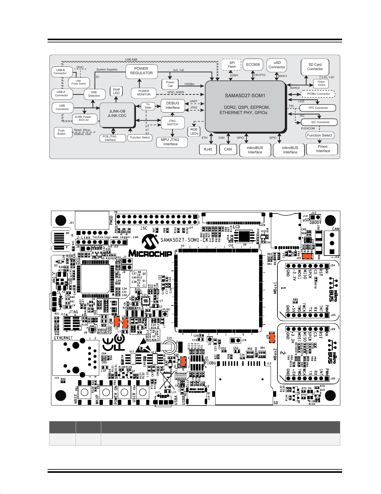
Figure 3-2. SAMA5D27 SOM1 Kit1 Block Diagram
PCB JTAG
Interface
SPI
Flash
System Supplies
POWER
REGULATOR
GPIO, SHDN
UART
MPU JTAG
Interface
JTAG
LCD
ISC
TWI
FLEXCOM
RJ45
ETH
CAN
CAN
mikroBUS
Interface
mikroBUS
Interface
GPIO
USB A&B
SDHC0
SDHC1
RGB
LEDs
USB
Detection
DEBUG
Interface
Push
Button
Reset, Wkup
DisBoot, User
Pmod
Interface
PIOBU Connector
ISC Connector
3v3, 1v8
Power
Cap
VDDBU
JTAG
SWITCH
USB-A
Connector
USB-B
Connector
uSD
Connector
SD Card
Connector
5V
GPIO
USB
Power Switch
3.3V, 1.8V
FPC Connector
POWER
MONITOR
SAMA5D27-SOM1
DDR2, QSPI, EEPROM,
ETHERNET PHY, GPIOs
JLINK-OB
JLINK-CDC
Dual
LED
Function Select
QSPI
GPIO
Function Select
Power
Switch
CRYPTO
ECC608
Tri
State
JLINK Power
5V/3.3V
USB
Connector
3.1.1 Default Jumper Settings
The figure below shows the default jumper settings. Jumpers in red are configuration items and current
measurement points. The following table describes the functionality of the jumpers.
SAMA5D27 SOM1 Kit1
Baseboard Components
Figure 3-3. Default Jumper Settings
Table 3-1. Jumper Settings
Jumper Default Function
J1 Closed VDD_MAIN_5V current measurement
© 2018 Microchip Technology Inc.
User Guide
DS50002667C-page 8
Page 9

...........continued
WARNING
Jumper Default Function
J2 Closed VDD_3V3 SOM current measurement
J4 Closed VDDBU current measurement
J7 Open Enables J-Link-OB (closed=disable)
Erases SAM3U firmware code (closed=erase at power-up)
SAMA5D27 SOM1 Kit1
Baseboard Components
J8 Open
J9 Open Enables JTAG-CDC (closed=disable)
J13 Open Disables SOM boot memories (closed=disable)
J22 Closed Enables 3.3V power mikroBUS1 (closed=enable)
J28 Closed Enables 3.3V power mikroBUS2 (closed=enable)
3.1.2 Baseboard Connectors
The following table describes the interface connectors on the SAMA5D27 SOM1 Kit1 baseboard.
Table 3-2. Baseboard Interface Connectors
Connector Interfaces to
J5 CLK_AUDIO test point (not populated)
J6 PCB-edge JTAG connector for factory-programming the J-Link-OB
J10 USB-A MicroAB, J-Link-OB port
J11 MPU SAMA5D27 JTAG 10-pin IDC connector
Must remain open. If closed, the SAM3U contents are erased and J-Link
functionality is discarded.
J12 Standard SDMMC0 connector
J14 microSD connector
J15 Ethernet RJ45 connector
J16 CAN 3-pin screw connector
J17 USB-A MicroAB connector
J18 HSIC 2-point header
J19 USB-B type C connector
J20-J23 Jumper to select Pmod functions
J21 Pmod connector
J24-25 mikroBUS1 connectors
J26 Expansion TFT LCD connector for display module
J27 ISC connector
© 2018 Microchip Technology Inc.
User Guide
DS50002667C-page 9
Page 10
...........continued
MPU + DDR2 1Gb
SAMA5D27C-D1G-CU
LFBGA289
64Mbit Serial QUAD I/O
Flash Memory
SST26VF064BT-104I/MF
1K Serial EEPROM
with EUI-48
Node Identity
24AA02E48T-I/OT
ΤΜ
10BASE-T / 100BASE-TX
PHY With RMII Support
KSZ8081RNAIA
Power Management
Unit
MIC2800-G1JJYML
VDDSDHC VDDISC VDDBU
MAIN
3.3V
TWI Interface
103 I/O Available
CLASS-D Stereo
eMMC Interface
QSPI Interface
Camera Interface
Up to 4 * ADC Inputs
TWI Interface
Up to 4 * UART
2 * SPI Interfaces
Up to 4 * FLEXCOM
LCD Interface up to 24-bit
SSC Interface
Mono PDMIC Interface
Up to 2 * CAN
I²S Interface
SDIO Interface
SD-CARD Interface
External
QSPI
Connection
JTAG & DBGU Interfaces
DEBUG
SYSTEM
MISC
USB Dev.
USB Host
HSIC
BACKUP
7 * PIOBU
RXD
WAKEUP
RESET
SHUTDOWN
CLK_AUDIO
COMPP / COMPN
Disable Boot
USB Device Connector
USB Host Connector
HSIC Device
Physical
Receiver
Transceiver
Interface
Connector Interfaces to
J29-J30 mikroBUS2 connectors
J31 Tamper and analog comparator connector
J32 SHDN test point (not populated)
3.2 Function Blocks
3.2.1 SAMA5D27 SOM1
The SAMA5D27 SOM1 main features are as follows:
• Ultra-small SIP (SAMA5D27-D1G-CU) embedding an ultra-low-power SAMA5D27 Arm® Cortex®A5 processor and a 1 Gbit DDR2 SDRAM memory
• SST26VF064 64 Mb QSPI Flash
• 24AA02E48 2 Kb serial E2PROM with preprogrammed EUI node identity
• MIC2800 power management device
• KSZ8081RNA Ethernet Phy 10/100 MHz RMII
SAMA5D27 SOM1 Kit1
Baseboard Components
Refer to the SAMA5D27 SOM1 datasheet for more information.
Figure 3-4. SAMA5D27 SOM1 Block Diagram
© 2018 Microchip Technology Inc.
User Guide
DS50002667C-page 10
Page 11

3.2.2 Power Supply Topology and Power Distribution
100k
0402
1%
R8
5
8 4
3
DMP2160
Q1B
1 2
J1
5
8 4
3
DMP2160
Q2B
0.1uF
50V
0402
C4
10k
0402
5%
R3
0.1uF
50V
0402
C9
2
71
6
DMP2160
Q2A
2
71
6
DMP2160
Q1A
100k
0402
1%
R12
0.1uF
50V
0402
C1
100k
0402
1%
R1
VBUS_JLINK VDD_MAIN_5V
VBUS_USBA
Shunt 2.54mm 1x2
CAUTION
3.2.2.1 Input Power Options
The board power source can come through either a USB connector (J10 or J17) connected to a PC or a
5V DC-USB power supply unit. These USB power sources are sufficient to supply the board in most
applications.
Important: In case of an external device connected through the USB-B port, it is
recommended to use the 5V DC-USB power supply unit as the main power source for the entire
system rather than a PC or a USB hub, which are limited to 500 mA typical.
The baseboard embeds a local power management stage comprising two sets of load switches,
respectively implemented by MOSFET DMP2160 and DC/DC converter MIC23451.
The following figure is a schematic of the power options.
Figure 3-5. Input Powering
SAMA5D27 SOM1 Kit1
Baseboard Components
Note: PC/USB-powered operation eliminates additional wires and batteries. It is the preferred mode of
operation for any project that requires only a 5V source at up to 500 mA.
Jumper J1 is used to perform MAIN_5V current measurements on the baseboard.
3.2.2.2 Power Supply Requirements and Restrictions
Detailed information on the device power supplies is provided in tables “SAMA5D2 Power Supplies” and
“Power Supply Connections” in the SAMA5D2 Series datasheet.
3.2.2.3 Power-up and Power-down Considerations
Power-up and power-down considerations are described in section “Power Considerations” of the
SAMA5D2 Series datasheet.
The power-up and power-down sequences provided in the SAMA5D2 Series datasheet must be
respected for reliable operation of the device. These are respected by the on-board MIC23451.
3.2.2.4 Power Management
The baseboard power management uses a MIC23451 PMIC, which is a triple synchronous buck regulator
with HyperLight Load® mode featuring a power good indicator. The triple DC-DC step down power
regulator delivers two outputs: 3.3V/2A and 1.8V/2A.
© 2018 Microchip Technology Inc.
User Guide
DS50002667C-page 11
Page 12

10uF
25V
0603
C2
0R
0402
R130
10k 04025%
R16
158k
0402
1%
R9
180R
L1
4.7uF
10V
0402
C6
180R
L2
309k
0402
1%
R11
10k
0402
5%
R10
1 2
HDR-2.54 Male 1x2
J1
0R0402
R17
1uH
L6
301k
0402
1%
R6
4.7uF
10V
0402
C8
71.5k
0402
1%
R5
100R
0402
5%
R4
0R0402
R19
10k
0402
5%
R13
10uF
25V
0603
C3
PGND
1
PGND
2
AVIN1
3
SW2
4
PVIN2
5
AVIN2
6
SW3
7
PVIN3
8
AVIN3
9
PGND10AGND
11
SNS3
12
PG3
13
FB3
14
EN3
15
PG2
16
FB2
17
SNS2
18
EN2
19
PG1
20
EN1
21
SNS1
22
FB1
23
AGND
24
PVIN1
25
SW1
26
MIC23451
U1
4.7uF10V
0402
C7
309k
0402
1%
R2
10k 04025%
R7
1 2
HDR-2.54 Male 1x2
J2
1uH
L8
10k 04025%
R18
10k 04025%
R15
10uF
25V
0603
C5
4.7uF
10V
0402
C10
71.5k
0402
1%
R14
180R
L7
1uH
L3
180R
L5
VOUT1
VOUT2 VDD_SDHC_1V8
VDDIN_3V3
VOUT3
VDD_3V3
VDD_MAIN_5V
VOUT2
VOUT1
VOUT3
VDD_SDHC_3V3
PD8
BB_PWR_GOOD
Shunt 2.54mm 1x2
JP2
Shunt 2.54mm 1x2
SAMA5D27 SOM1 Kit1
Baseboard Components
While the external power is being applied, the baseboard can be shut down by software and then woken
up by action on the PB2 push button, which activates the WKUP signal.
The figure below shows the power management scheme.
Figure 3-6. Baseboard Power Management
One PIO (PD8) is used to check the status of the main regulator.
Table 3-3. Power Good Signal
PIO Mnemonic Signal Description
PD8 BB_PWR_GOOD High level = power is established
3.2.2.5 Supply Group Configuration
The main regulator provides the 3.3V for the SOM and all power supplies required by the baseboard:
• 3.3V SOM (VDDIN_3V3)
• 3.3V VDDSDHC (3.3V or 1.8V)
• 3.3V baseboard (VDD_3V3)
• 3.3V VDDBU
© 2018 Microchip Technology Inc.
and at correct level
User Guide
DS50002667C-page 12
Page 13
Figure 3-7. SOM Power Lines
2.2uF
16V
0603
C21
0.1uF
50V
0402
C17
0.1uF
50V
0402
C24
0.1uF
50V
0402
C18
2.2uF
16V
0603
C16
2.2uF
16V
0603
C19
0.1uF
50V
0402
C20
2.2uF
16V
0603
C23
0.1uF
50V
0402
C22
VDDIN_3V3
VDDBU
VDDSDHC
VDDIN_3V3
VDDBU
55
VDDIN_3V3_1
16
VDDIN_3V3_2
17
VDDISC
15
VDDSDHC
65
GND_1
10
GND_2
18
GND_3
26
GND_4
31
GND_5
39
GND_6
42
GND_7
43
GND_8
50
GND_9
56
GND_10
62
GND_11
66
GND_12
69
GND_13
72
GND_14
75
GND_15
88
GND_16
89
GND_17
98
GND_18
107
GND_19
130
GND_20
131
GND_21
149
GND_22
166
GND_23
171
GND_24
176
GND_0
1
SAMA5D27-SOM1
U3F
BAT54C
2
3
1
D1
1 2
HDR-2.54 Male 1x2
J4
220mF
3.3V
P8.3L11.7D6.8H1.8
C14
0.1uF
50V
0402
C13
RB160M-60TR
D2
100R
0402
5%
R20
VDDBU
VDD_3V3
(Super)-Capacitor
energy storage
Shunt 2.54mm 1x2
JP3
0R DNP
0402
R131
100k
0402
1%
R132
100k
0402
1%
R129
3
1
2
BSS138
Q7
3
1
2
BSS138
Q6
10k
0402
5%
R128
10k
0402
5%
R127
1 4
2
3
TACT SPST
PB3
VDDBU VDD_MAIN_5V
SHDN
POWER
ON
3.2.2.6 Backup Power Supply
The baseboard features a power source in order to permanently power the backup area of the SAMA5D2
device (refer to the SAMA5D2 Series datasheet). A super capacitor (C14) sustains such permanent
power to VDDBU when all system power sources are off.
Figure 3-8. VDDBU Powering Options
SAMA5D27 SOM1 Kit1
Baseboard Components
3.2.3 Shutdown Circuitry
On the baseboard, this circuitry is implemented but inhibited by default (R131 is not populated).
The SHDN signal, output of the shutdown controller, signals the shutdown request to the power supply.
This output signal is supplied by VDDBU that is present in Backup mode.
The shutdown controller manages the main power supply and is connected to the ENABLE input pin of
the DC/DC converter providing the main power supplies of the system.
Figure 3-9. Shutdown Controller
3.2.4 Push Button Switches
The baseboard features four push buttons:
© 2018 Microchip Technology Inc.
User Guide
DS50002667C-page 13
Page 14
100R
0402
5%
R23
100k
0402
1%
R126
100R
0402
5%
R24
10k
0402
5%
R121
1 4
2 3
TACT SPST
PB1
1 4
2 3
TACT SPST
PB2
VDDBU
VDDBU
NRST
WKUP
NRST
WAKE UP
1 4
2 3
TACT SPST
PB4
100R
DNP
04025%
R72
100R 04025%
R73
PIOBU1
PA29
CS_QSPI1
10k
0402
5%
R53
0.1uF
50V
0402
C52
10k
0402
5%
R54
VDD_3V3
VDD_3V3
PB5
PB7
PB8
PB9
PB10
QSPI Flash
QSPI1_SCK
QSPI1_IO0
QSPI1_IO1
QSPI1_IO2
QSPI1_IO3
CE
1
SO/SIO1
2
WP/SIO2
3
VSS4SI/SIO0
5
SCK
6
HOLD/SIO3
7
VDD
8
SST26VF064B
U9 DNP
VDD_3V3
SAMA5D27 SOM1 Kit1
Baseboard Components
• One reset push button (PB1). When pressed and released, the baseboard is reset.
• One wake-up push button (PB2) connected to the SAMA5D27 WKUP pin, used to exit the
processor from Backup mode.
• One power-on button (PB3).
Figure 3-10. System Push Buttons
• One user momentary push button (PB4) connected to PIO PA29, and optionally to PIOBU1.
The wake-up is available only if the shutdown controller is used (see figure Shutdown Controller).
Figure 3-11. User Push Button
3.2.5 Additional Memories
One additional memory, QSPI device U9, can be soldered on the baseboard. This QSPI Flash memory
uses the same PIOs as the SOM QSPI. Such configuration makes it possible to choose between two
bootable memories.
The figure below illustrates the QSPI memory implementation.
Figure 3-12. Optional QSPI Serial Data Flash on Baseboard
Table 3-4. QSPI Signal Descriptions
PIO Mnemonic Shared PIO Signal Description
PB5 QSPI1_SCK QSPI on SOM Clock
PB6 QSPI1_CS QSPI on SOM Chip select
PB7 QSPI0_IO0 QSPI on SOM Data0
PB8 QSPI0_IO1 QSPI on SOM Data1
PB9 QSPI0_IO2 QSPI on SOM Data2
PB10 QSPI0_IO3 QSPI on SOM Data3
© 2018 Microchip Technology Inc.
User Guide
DS50002667C-page 14
Page 15

3.2.5.1 CS Disable Boot
PB6
CS_QSPI1
1 2
HDR-2.54 Male 1x2
J13
10k
0402
5%
R59
10k
0402
5%
R60
0.1uF
50V
0402
C55
OE
1
A
2
Y
4
GND
3
VCC
5
NL17SZ125-D
U10
DNP
VDD_3V3
VDD_3V3
DISABLE_BOOT
PB6
QSPI1_CS
(SOM)
One jumper (J13) controls the selection (CS#) of the bootable memory components (QSPI) using a noninverting 3-state buffer.
Figure 3-13. CS Disable Boot
The rule of operation is:
• PB1 (RESET) pressed and J13 open = booting from QSPI on SOM
• PB1 (RESET) pressed and J13 closed = booting from QSPI on baseboard if fitted. The QSPI on
SOM is disabled.
Refer to the SAMA5D2 Series datasheet for more information on standard boot strategies and
sequencing.
SAMA5D27 SOM1 Kit1
Baseboard Components
3.2.6 Secure Digital Multimedia Card (SDMMC) Interface
The SD (Secure Digital) Card is a non-volatile memory card format used as a mass storage memory in
mobile devices.
3.2.6.1 Secure Digital Multimedia Card (SDMMC) Controller
The baseboard features two Secure Digital Multimedia Card (SDMMC) interfaces that support the
MultiMedia Card (e.MMC) Specification V4.41, the SD Memory Card Specification V3.0, and the SDIO
V3.0 specification. It is compliant with the SD Host Controller Standard V3.0 Specification.
• The SDMMC0 interface is connected to a standard SD card interface.
• The SDMMC1 interface is connected to a microSD card interface.
3.2.6.2 SDMMC0 Card Connector (J12)
A standard MMC/SD card connector, connected to SDMMC0, is mounted on the top side of the
baseboard. The SDMMC0 communication is based on a 12-pin interface (clock, command, write protect,
power switch and data (8)). A card detection switch is included.
The figure below illustrates the SDMMC0 interface implementation.
© 2018 Microchip Technology Inc.
User Guide
DS50002667C-page 15
Page 16

Figure 3-14. SDMMC0
10k
0402
5%
R56
0R
0402
R52
10k
0402
5%
R58
10uF
25V
0603
C53
123
4 5
678
68k
1206
5%
RR2
0.1uF
50V
0402
C54
1
2
3
4 5
6
7
8
68k
1206
5%
RR1
10k
0402
5%
R57
VDDSDHC
VDD_3V3
PA0
PA1
PA2
PA3
PA4
PA5
PA6
PA7
PA8
PA9
PA12
PA13
SDMMC0_CD
SDMMC0_DA1
SDMMC0_DA0
SDMMC0_CK
SDMMC0_CDA
SDMMC0_DA3
SDMMC0_DA2
SDMMC0_DA4
SDMMC0_DA5
SDMMC0_DA6
SDMMC0_DA7
SDMMC0_WP
8
5
7
6
4
3
2
1
9
14
15
16
13
12
11
10
J12
SD_MMCPlus_CARD
Figure 3-15. Standard SD Socket J12 Location
SAMA5D27 SOM1 Kit1
Baseboard Components
The table below describes the pin assignment of SDMMC connector J12.
Table 3-5. Standard SD Socket J12 Pin Assignment
© 2018 Microchip Technology Inc.
Pin No Mnemonic PIO Signal Description
1 SDMMC0_DAT3_PA5 PA5 Data line
2 SDMMC0_CMD_PA1 PA1 Command/response line
User Guide
DS50002667C-page 16
Page 17

...........continued
10k
0402
5%
R62
0.1uF
50V
0402
C57
DAT2
P1
CD/DAT3
P2
CMD
P3
VDD
P4
CLK
P5
VSS
P6
DAT0
P7
DAT1
P8
POL
G4
DET
G5
GND
G1
GND
G2
GND
G3
GND
G6
DM3AT-SF-PEJM5
J14
CON FLASH Micro SD Card w DET + GND
0R
0402
R61
10k
0402
5%
R63
10uF
25V
0603
C56
1
2
3
4 5
678
68k
1206
5%
RR3
VDD_3V3
PA18
PA19
PA20
PA21
PA22
PA28
PA30
SDMMC1_CD
SDMMC1_DAT0
SDMMC1_DAT1
SDMMC1_CK
SDMMC1_CDA
SDMMC1_DAT3
SDMMC1_DAT2
Pin No Mnemonic PIO Signal Description
3 GND – GND
SAMA5D27 SOM1 Kit1
Baseboard Components
4
VDDSDHC (3.3V or
1.8V)
5 SDMMC0_CK_PA0 PA0 Clock line
6 SDMMC0_CD_PA13 PA13 Card detect
7 SDMMC0_DAT0_PA2 PA2 Data line
8 SDMMC0_DAT1_PA3 PA3 Data line
9 SDMMC0_DAT2_PA4 PA4 Data line
10 SDMMC0_DAT4_PA6 PA6 Data line
11 SDMMC0_DAT5_PA7 PA7 Data line
12 SDMMC0_DAT6_PA8 PA8 Data line
13 SDMMC0_DAT7_PA9 PA9 Data line
14 SDMMC0_WP_PA12 PA12 Write protect signal
15 GND – GND
16 GND – GND
Table 3-6. SDMMC1 Power Command
–
Power line
PIO Mnemonic Signal Description
PA11 SDMMC0_VDDSEL Select 3.3V or 1.8V
3.2.6.3 SDMMC1 Card Connector (J14)
A microSD card connector, connected to SDMMC1, is mounted on the top side of the baseboard. The
SDMMC1 communication is based on a 6-pin interface (clock, command and four data). A card detection
switch is included. The microSD connector can be used to connect any microSD card for mass storage.
Figure 3-16. SDMMC1 microSD
© 2018 Microchip Technology Inc.
User Guide
DS50002667C-page 17
Page 18

Figure 3-17. microSD Socket J14 Location
SAMA5D27 SOM1 Kit1
Baseboard Components
The table below describes the pin assignment of microSD connector J14.
Table 3-7. microSD Socket J14 Pin Assignment
Pin No Mnemonic PIO Signal Description
1 SDMMC1_DAT2 PA20 Data bit 2
2 SDMMC1_DAT3 PA21 Data bit 3
3 SDMMC1_CDA PA28 Command
4 VCC – 3.3V supply voltage
5 SDMMC1_CK PA22 Clock
6 GND – Common ground
7 SDMMC1_DAT0 PA18 Data bit 0
8 SDMMC1_DAT1 PA19 Data bit 1
9 SW1 GND Ground
10 SDMMC1_CD PA30 Card detection switch
11 GND – Common ground
© 2018 Microchip Technology Inc.
User Guide
DS50002667C-page 18
Page 19

ATECC608A-SSHDA
GND
4
SDA
5
SCL
6
VCC
8
U11
0.1uF
50V
0402
C58
VDD_3V3
PD21
PD22
TWD0
TWCK0
SAMA5D27 SOM1 Kit1
...........continued
Pin No Mnemonic PIO Signal Description
12 GND – Common ground
13 GND – Common ground
14 GND – Common ground
Baseboard Components
3.2.6.4 CryptoAuthentication
ATECC608A is a member of the CryptoAuthentication family of crypto engine authentication devices with
highly secure hardware-based key storage.
The ATECC608A features a flexible command set enabling use in many applications, including
network/IoT node protection, anti-counterfeiting, firmware or media protection, secure data storage and
user password checking.
The device (U11) is mounted in an 8-lead UDFN package.
For more information, refer to the ATECC608A datasheet on www.microchip.com.
Figure 3-18. CryptoAuthentication ATECC608
Table 3-8. ATECC608 PIO Signal Descriptions
PIO Mnemonic Shared Signal Description
PD21 TWD0 SOM E2PROM
PD22 TWCK0 SOM E2PROM
™
TWI data
24AA02E48
TWI clock
24AA02E48
3.2.7 Communication Interfaces
This section describes the signals and connectors related to the ETH, USB and CAN communication
interfaces.
3.2.7.1 Ethernet 10/100 (GMAC) Port
The on-board SOM integrates a 10/100 Mbps Ethernet controller (KSZ8081RNA) allowing direct
connection to any 10/100 Mbps Ethernet-based Local Area Network, for full interaction with local servers
and wide area networks such as the Internet.
ETH signals from the SOM are connected to a RJ45 MagJack. Additionally, for monitoring and control
purposes, a LED functionality is carried on the RJ45 connector to indicate link status.
© 2018 Microchip Technology Inc.
User Guide
DS50002667C-page 19
Page 20

Figure 3-19. Ethernet PHY
ETH_LED0
0.1uF
50V
0402
C64
0.1uF
50V
0402
C63
470R
R69
EARTH_ETH
EARTH_ETH
GND_ETH
VDD_3V3
ETH_LED0
TX+
TX-
RX+
RX-
LINK
1
2
3
6
4
5
7
8
75
75
75 75
1nF
TD+
TD-
CT
NC
RD-
CT
TX+
TX-
RX+
RX-
RD+
Left Green LEDRight yellow LED
1
2
7
8
3
6
5
4
9
10
11
12
13
14
15
16
RJ45
J15
RJ45 J00-0061
TX_P
TX_N
RX_N
RX_P
Figure 3-20. Ethernet RJ45 Connector J15 Location
SAMA5D27 SOM1 Kit1
Baseboard Components
The table below describes the pin assignment of Ethernet connector J15.
Table 3-9. Ethernet RJ45 Connector J15 Pin Assignment
Pin No Mnemonic Signal Description
1 TX+ Transmit positive differential pair
2 TX- Transmit negative differential pair
3 RX+ Receive positive differential pair
© 2018 Microchip Technology Inc.
User Guide
DS50002667C-page 20
Page 21

SAMA5D27 SOM1 Kit1
...........continued
Pin No Mnemonic Signal Description
4 Decoupling capacitor –
5 Decoupling capacitor –
6 RX- Receive negative differential pair
7 NC –
8 EARTH / GND Common ground
9 ACT LED (A) LED activity (not used)
10 ACT LED (K) LED activity (not used)
11 LINK LED (K) LED link connection
12 LINK LED (A) LED link connection
13 EARTH / GND Common ground
14 EARTH / GND Common ground
Baseboard Components
15 NC –
16 NC –
3.2.7.2 USB Interfaces
The USB (Universal Serial Bus) is a hot-pluggable general-purpose high-speed I/O standard for computer
peripherals. The standard defines connector types, cabling, and communication protocols for
interconnecting a wide variety of electronic devices. The USB 2.0 Specification defines data transfer rates
as high as 480 Mbps (also known as High Speed USB). A USB host bus connector uses 4 pins: a power
supply pin (5V), a differential pair (D+ and D- pins) and a ground pin.
The baseboard features three USB communication ports named USB-A to USB-C:
• USB-A device interface
– One USB device standard micro-AB connector.
– This port offers a VBUS detection function through the R81-R83 resistor ladder.
– The USB-A port is used as a secondary power source and as a communication link for the
baseboard, and derives power from the PC over the USB cable. In most cases, this port is
limited to 500 mA.
• USB-B (host port B high- and full-speed interface)
– One USB host type C connector.
– The USB-B host port is equipped with a 500 mA high-side power switch.
• USB-C (High-Speed Inter-Chip/HSIC port)
– One USB high-speed host port with an HSIC interface.
– The port is connected to a single 2-pin header (not populated).
3.2.7.3 USB-A Interface
The figure below shows the USB implementation on the USB-A port terminated on a micro USB type
microAB connector.
© 2018 Microchip Technology Inc.
User Guide
DS50002667C-page 21
Page 22

100k
0402
1%
R70
USB2.0 MICRO-B FEMALE
ID
4
VBUS
1
GND
5
D-
2
D+
3
0
J17
20pF
50V
0402
C65
0.1uF
50V
0402
C12
200k
0402
1%
R71
EARTH_USB_A
VBUS_USBA
USBA_DM
USBA_DP
PD20
USBA_VBUS_5V
USBA_N
USBA_P
SAMA5D27 SOM1 Kit1
Baseboard Components
The USB-A port (J17) features a VBUS insert detection function through ladder-type resistors R70 and
R71.
Figure 3-21. USB-A Type microAB Connector
Table 3-10. USB-A PIO Signal Description
PIO Mnemonc Shared Signal Description
PD20 USBA_VBUS_5V – VBUS insertion
detection
Figure 3-22. USB-A Type microAB Connector J17 Location
The table below describes the pin assignment of USB-A connector J17.
© 2018 Microchip Technology Inc.
User Guide
DS50002667C-page 22
Page 23

Table 3-11. USB-A Connector J17 Pin Assignment
USBB_VBUS_5V
36k
0402
1%
R79
330pF
0402
C69
VBUS1
A4
GND8
28
GND5
25
GND3
B12
GND2
A12
GND1
A1
VBUS4
B4
VBUS2
A9
VBUS3
B9
GND4
B1
TX1+
A2
TX1-
A3
RX1+
B11
RX1-
B10
D1+
A6
D1-
A7
D2+
B6
D2-
B7
CC1
A5
TX2+
B2
TX2-
B3
RX2+
A11
RX2-
A10
SBU1
A8
SBU2
B8
CC2
B5
GND7
27
GND6
26
USB 3.1 C
J19
36k
0402
1%
R78
330pF
0402
C70
EARTH_USB_B
EARTH_USB_B
VDD_3V3
USBB_DP
USBB_DM
USBB_P
USBB_N
Pin No Mnemonic Signal Description
1 VBUS 5V power
2 DM Data minus
3 DP Data plus
4 ID On-the-go identification
5 GND Common ground
3.2.7.4 USB-B Interface
The figure below shows the USB implementation on the USB-B port terminated on USB Type C
connector J19.
Figure 3-23. USB-B Type C Connector
SAMA5D27 SOM1 Kit1
Baseboard Components
© 2018 Microchip Technology Inc.
User Guide
DS50002667C-page 23
Page 24

Figure 3-24. USB-B Type C Connector J19 Location
SAMA5D27 SOM1 Kit1
Baseboard Components
The table below describes the pin assignment of USB-B connector J19.
Table 3-12. USB-B Connector J19 Pin Assignment
Pin No Mnemonic Signal Description
A1 GND Ground return
A2 SSTXp1 SuperSpeed differential pair #1, TX, positive (NOT USED)
A3 SSTXn1 SuperSpeed differential pair #1, TX, negative (NOT USED)
A4 VBUS Bus power
A5 CC1 Configuration channel
A6 DP1 USB 2.0 differential pair, position 1, positive
A7 DN1 USB 2.0 differential pair, position 1, negative
A8 SBU1 Sideband use (SBU)
A9 VBUS Bus power
A10 SSRXn2 SuperSpeed differential pair #2, RX, negative (NOT USED)
A11 SSRXp2 SuperSpeed differential pair #2, RX, positive (NOT USED)
© 2018 Microchip Technology Inc.
User Guide
DS50002667C-page 24
Page 25

USBB_VBUS_5V
EN
1
FLG2GND
3
NC
4
NC
5
OUT6IN
7
OUT
8
USB Power Switch
U13
10k
0402
5%
R138
10uF
25V
0603
C67
0.1uF
50V
0402
C68
180R
L12
0.1uF
50V
0402
C66
10k
0402
5%
R77
VDD_MAIN_5V
VDD_3V3
PD19
PA27
EN:Active High
USBB_POWR_EN
USBB_OVCUR
SAMA5D27 SOM1 Kit1
Baseboard Components
...........continued
Pin No Mnemonic Signal Description
A12 GND Ground return
B12 GND Ground return
B11 SSRXp1 SuperSpeed differential pair #1, RX, positive (NOT USED)
B10 SSRXn1 SuperSpeed differential pair #1, RX, negative (NOT USED)
B9 VBUS Bus power
B8 SBU2 Sideband use (SBU)
B7 DN2 USB 2.0 differential pair, position 2, negative
B6 DP2 USB 2.0 differential pair, position 2, positive
B5 CC2 Configuration Channel
B4 VBUS Bus power
B3 SSTXn2 SuperSpeed differential pair #2, TX, negative (NOT USED)
B2 SSTXp2 SuperSpeed differential pair #2, TX, positive (NOT USED)
B1 GND Ground return
3.2.7.4.1 USB-B Power Switch
The USB-B Host port is equipped with a 500 mA high-side power switch for self-powered and buspowered applications. If the client device is bus-powered, the carrier can supply a 5V, 500mA power to
the client device. The USBB_EN_5V_PA27 signal controls the power switch and current limiter, the
Microchip MIC2025, which in turn supplies power to a bus-powered client device. Per the USB
specification, bus-powered USB 2.0 devices are limited to a maximum of 500 mA. The MIC2025 limits the
current and indicates an overcurrent with the USBB_OVCUR_PD19 signal.
Figure 3-25. USB-B Power Switch
Table 3-13. Power Switch PIO Signal Descriptions
PIO Mnemonic Shared Signal Description
PA27 USBB_POWR_EN USBB_EN_5V
PD19 USBB_OVCUR
© 2018 Microchip Technology Inc.
– Power switch enable
(active high)
– Indicates overcurrent
(open drain)
User Guide
DS50002667C-page 25
Page 26

3.2.7.5 HSIC Interface
1 2
HDR-2.54 Male 1x2
J18
HSIC_DATA
HSIC_STRB
62R
1210
1%
R66
0R
0402
R68
0.1uF
50V
0402
C59
0.1uF
50V
0402
C61
1
2
3
1727023
J16
4.7uF
10V
0402
C60
62R
1210
1%
R67
0R
0402
R65
15pF
50V
0402
C62
VDD_3V3
VDD_MAIN_5V
PC26
PC27
CANTX1
CANRX1
RXD
4
TXD
1
GND
2
VCC
3
VIO
5
CANL
6
CANH
7
STBY
8
EP
9
ATA6561-GBQW
U12
High-Speed Inter-Chip (HSIC) is a standard for USB chip-to-chip interconnect with a 2-signal (strobe,
data) source synchronous serial interface using 240 MHz DDR signaling to provide only high-speed 480
Mbps data rate.
The interface operates at high speed, 480 Mbps, and is fully compatible with existing USB software
stacks. It meets all data transfer needs through a single unified USB software stack.
The HSIC interface is connected to two-point header J18. This connector is not mounted.
Figure 3-26. HSIC Interface J18
3.2.7.6 CAN Interface
This section lists the signals related to the Controller Area Network (CAN) interface.
The CAN interface transmits and receives signals from the SOM. CAN PIOs PC26 and PC27 are
connected to the CAN transceiver (ATA6561) and the output signals from the transceiver are connected
to the screw connector (J16) physically located on top of the baseboard.
SAMA5D27 SOM1 Kit1
Baseboard Components
Figure 3-27. CAN Interface
© 2018 Microchip Technology Inc.
User Guide
DS50002667C-page 26
Page 27

Figure 3-28. CAN Connector J16 Location
SAMA5D27 SOM1 Kit1
Baseboard Components
Table 3-14. CAN Connector J16 Pin Assignment
Pin Mnemonic Signal Description
1 CANH Differential positive
2 CANL Differential negative
3 GND Ground
3.3 External Interfaces
3.3.1 LCD TFT Interface
The baseboard provides a FPC connector with 24 bits of data and control signals to the LCD interface.
Other signals are used to control the LCD and are available on connector J26: TWI, SPI, two GPIOs for
interrupt, 1-wire and power supply lines.
This connector is used to connect LCD display type TM43xx series, TM5000 series or TM7000 series
from PDA Inc. (www.pdaatl.com).
A 50-pin FPC (J26) header is provided on the baseboard to interface the LCD module with 24-bit parallel
RGB.
The connector provides two PIOs as interrupts, one SPI and a TWI port to interface the MaXTouch
touch controller or QTouch® button controller embedded on the LCD module.
®
In order to operate correctly out of the processor with various LCD modules, two voltage lines are
available: 3.3V and 5VCC (default). Both are selected by 0R resistors R81 and R83.
© 2018 Microchip Technology Inc.
User Guide
DS50002667C-page 27
Page 28

Figure 3-29. LCD Expansion Header Interface
TWD_LCD
TWCK_LCD
0R0402
R81 DNP
100R
0402
5%
R119
0R0402
R85
0R0402
R83
VDD_3V3VDD_MAIN_5V
PB12
PB13
PB14
PB15
PB16
PB17
PB18
PB19
PB20
PB21
PB22
PB23
PB24
PB25
PB26
PB27
PB28
PB29
PB30
PB31
PC0
PC1
PC2
PC5
PC6
PC7
PC8
PA14
PC4
PA15
PA16
PA17
PD1
PC25
LCD_PWM_PC3
NRST
PB11
PA17
SPI0_ SPCK
SPI0_ MOSI
SPI0_ MISO
SPI0_NPCS0
LCDDAT0
LCDDAT6
LCDDAT5
LCDDAT4
LCDDAT3
LCDDAT2
LCDDAT1
LCDDAT11
LCDDAT10
LCDDAT9
LCDDAT8
LCDDAT7
LCDDAT16
LCDDAT15
LCDDAT14
LCDDAT13
LCDDAT12
LCDDAT22
LCDDAT21
LCDDAT20
LCDDAT19
LCDDAT18
LCDDAT17
LCDDEN
LCDHSYNC
LCDVSYNC
LCDPCK
LCDDAT23
IRQ1
IRQ2
LCDPWM
LCDDISP
1
2
3
4
5
6
7
8
9
10
11
12
13
14
15
16
17
18
19
20
21
22
23
24
25
26
27
28
29
30
31
32
33
34
35
36
37
38
39
40
41
42
43
44
45
46
47
48
49
50
MNT
FFC
FFC/FPC 50P Female
J26
SAMA5D27 SOM1 Kit1
Baseboard Components
© 2018 Microchip Technology Inc.
User Guide
DS50002667C-page 28
Page 29

Figure 3-30. LCD Connector J26 Location
SAMA5D27 SOM1 Kit1
Baseboard Components
The table below describes the pin assignment of LCD connector J26.
Table 3-15. LCD Connector J26 Pin Assignment
Pin No Signal PIO Signal RGB Interface Function
1 ID PA17 ID Shared with SPI_NPCS0 pin 40
2 GND GND GND GND
3 LCDDAT0 PB11 D0 Data line (BLUE0)
4 LCDDAT1 PB12 D1 Data line (BLUE1)
5 LCDDAT2 PB13 D2 Data line (BLUE2)
6 LCDDAT3 PB14 D3 Data line (BLUE3)
7 – – GND GND
8 LCDDAT4 PB15 D4 Data line (BLUE4)
9 LCDDAT5 PB16 D5 Data line (BLUE5)
10 LCDDAT6 PB17 D6 Data line (BLUE6)
11 LCDDAT7 PB18 D7 Data line (BLUE7)
© 2018 Microchip Technology Inc.
User Guide
DS50002667C-page 29
Page 30

SAMA5D27 SOM1 Kit1
Baseboard Components
...........continued
Pin No Signal PIO Signal RGB Interface Function
12 – GND GND GND
13 LCDDAT8 PB19 D8 Data line (GREEN0)
14 LCDDAT9 PB20 D9 Data line (GREEN1)
15 LCDDAT10 PB21 D10 Data line (GREEN2)
16 LCDDAT11 PB22 D11 Data line (GREEN3)
17 – – GND GND
18 LCDDAT12 PB23 D12 Data line (GREEN4)
19 LCDDAT13 PB24 D13 Data line (GREEN5)
20 LCDDAT14 PB25 D14 Data line (GREEN6)
21 LCDDAT15 PB26 D15 Data line (GREEN7)
22 – GND GND GND
23 LCDDAT16 PB27 D16 Data line (RED0)
24 LCDDAT17 PB28 D17 Data line (RED1)
25 LCDDAT18 PB29 D18 Data line (RED2)
26 LCDDAT19 PB30 D19 Data line (RED3)
27 – – GND GND
28 LCDDAT20 PB31 D20 Data line (RED4)
29 LCDDAT21 PC0 D21 Data line (RED5)
30 LCDDAT22 PC1 D22 Data line (RED6)
31 LCDDAT23 PC2 D23 Data line (RED7)
32 – GND GND GND
33 LCDPCK PC7 PCLK Pixel clock
34 LCDVSYNC PC5 VSYNC/CS Vertical sync
35 LCDHSYNC PC6 HSYNC/WE Horizontal sync
36 LCDDEN PC8 DATA_ENABLE Data enable
37 SPI_SPCK PA14 SPI_SCK SPI clock
38 SPI_MOSI PA15 SPI_MOSI SPI Master OUT Slave IN
39 SPI_MISO PA16 SPI_MISO SPI Master IN Slave OUT
40 SPI_NPCS0 PA17 SPI_CS SPI chip select
41 LCDDISP PC4 ENABLE Display enable signal
42 TWD PD4 TWI_SDA I2C data line (maXTouch)
© 2018 Microchip Technology Inc.
User Guide
DS50002667C-page 30
Page 31

...........continued
TWD_ISC
PC22
PC21
PC19
TWCK_ISC
PC18
PC20
1
2
3
4
5
6
7
8
9
10
11
12
13
14
15
16
17
18
19
20
22
2123
24
25
26
27
28
29
30
J27
VDD_3V3
PC9
PC10 PC11
PC12 PC13
PC14 PC15
PC16 PC17
PC23
PC24
PD6 PD7
ISC_D10
ISC_D8
ISC_D6
ISC_D4
ISC_D2
ISC_D0
ISC_PCK
ISC_HSYNC
ISC_VSYNC
ISC_MCK
ISC_PWD
ISC_D11
ISC_D9
ISC_D7
ISC_D5
ISC_D3
ISC_RST
ISC_D1
Pin No Signal PIO Signal RGB Interface Function
43 TWCK PD5 TWI_SCL I2C clock line (maXTouch)
44 GPIO PD1 IRQ1 maXTouch interrupt line
45 GPIO PC25 IRQ2 Interrupt line for other I2C devices
46 LCDPWM PC3 PWM Backlight control
47 RESET nRST RESET Reset for both display and maXTouch
48 Main_5V/3V3 VCC VCC 3.3V or 5V supply (R81/R83 selected)
49 Main_5V/3V3 VCC VCC 3.3V or 5V supply (R81/R83 selected)
50 GND GND GND GND
3.3.2 Image Sensor (ISC) Interface
This section describes the signals and connectors related to the ISC interface.
The Image Sensor Controller (ISC) system manages incoming data from a parallel or serial CSI-2 based
CMOS/CCD sensor. The system supports a single active interface, as well as the ITU-R BT 656/1120 422
protocol with an 8-bit or 10-bit data width and raw Bayer format. The internal image processor includes
adjustable white balance, color filter array interpolation, color correction, gamma correction, 12-bit to 10bit compression, programmable color space conversion, as well as horizontal and vertical chrominance
subsampling module.
SAMA5D27 SOM1 Kit1
Baseboard Components
Figure 3-31. ISC Interface
© 2018 Microchip Technology Inc.
User Guide
DS50002667C-page 31
Page 32

Figure 3-32. ISC Connector J27 Location
SAMA5D27 SOM1 Kit1
Baseboard Components
The table below describes the pin assignment of ISC connector J27.
Table 3-16. ISC Connector J27 Pin Assignment
SAMA5D27 Signal Pin No Signal SAMA5D27
Function PIO PIO Function
3.3V power – VDD_3V3 1 2 GND – Ground
3.3V power – VDD_3V3 3 4 GND – Ground
Reset PD6 ISC_RST 5 6 ISC_PWD PD7 Power
down
TWI clock PD5 TWCK_ISC 7 8 TWD_ISC PD4 TWI data
Ground – GND 9 10 ISC_MCK PC24 Master
clock
Ground – GND 11 12 ISC_VSYNCPC22 Vertical
sync
Ground – GND 13 14 ISC_HSYNCPC23 Horizontal
sync
© 2018 Microchip Technology Inc.
User Guide
DS50002667C-page 32
Page 33

...........continued
2.2k
0402
5%
R74
10k
0402
5%
R137
3
1
2
BSS138
Q9
100R
0402
5%
R136
GREEN
BLUE
2
1
RED
4
3
RED, GREEN, BLUE
D5
LED_RGB_CLV1A
3
1
2
BSS138
Q8
3
1
2
BSS138
Q10
100R
0402
5%
R135
1k
0402
5%
R76
10k
0402
5%
R133
100R
0402
5%
R134
2.2k
0402
5%
R75
VDD_3V3
PB1
PA31
PA10
LED_Red
LED_Green
LED_blue
SAMA5D27 Signal Pin No Signal SAMA5D27
Function PIO PIO Function
Ground – GND 15 16 ISC_PCK PC21 Clock
Ground – GND 17 18 ISC_D0 PC9 Data0
Data1 PC10 ISC_D1 19 20 ISC_D2 PC11 Data2
Data3 PC12 ISC_D3 21 22 ISC_D4 PC13 Data4
Data5 PC14 ISC_D5 23 24 ISC_D6 PC15 Data6
Data7 PC16 ISC_D7 25 26 ISC_D8 PC17 Data8
Data9 PC18 ISC_D9 27 28 ISC_D10 PC19 Data10
Data11 PC20 ISC_D11 29 30 GND – Ground
Note: ISC and LCD share the same TWI interface.
3.3.3 RGB LED
The baseboard features one RGB LED which can be controlled by the user. The three LED cathodes are
controlled via GPIO PWM or timer/counter pins.
SAMA5D27 SOM1 Kit1
Baseboard Components
Figure 3-33. RGB LED Indicators
Table 3-17. RGB LED PIOs
Signal Shared PIO Function
LED_RED – PA10 TIOA1
LED_GREEN PWM MBUS1 PB1 PWML1
3.4 Debugging Capabilities
The baseboard includes two main debugging interfaces to provide debug-level access to the SAMA5D2:
© 2018 Microchip Technology Inc.
LED_BLUE PWM MBUS2 PA31 PWML0
User Guide
DS50002667C-page 33
Page 34

• One UART through USB J-Link-CDC
JTAG_TDO
NRST
JTAG_TMS
JTAG_TDI
JTAG_TCK
RTCK_IN
100k
0402
1%
R48
100k
0402
1%
R46
100k
0402
1%
R47
100R
0402
5%
R51
1
2
3
4
5
6
7
8
9
10
HDR-1.27 Male 2x5
J11
0R
0402
R50
10k
0402
5%
R120
VDD_3V3
VDD_3V3
• Two JTAG interfaces, one connected from the MPU using connector J11 and one through the JLink-OB interface USB port J10
3.4.1 Debug JTAG
This section describes the signals and connectors related to the JTAG interface.
A 10-pin JTAG header is provided on the baseboard to facilitate software development and debugging
using various JTAG emulators. The interface signals have a voltage level of 3.3V.
Figure 3-34. JTAG Interface
Figure 3-35. JTAG Connector J11 Location
SAMA5D27 SOM1 Kit1
Baseboard Components
The table below describes the pin assignment of JTAG connector J11.
Table 3-18. JTAG/ICE Connector J11 Pin Assignment
Pin No Mnemonic Signal Description
1 VTref. 3.3V power This is the target reference voltage (main 3.3V).
© 2018 Microchip Technology Inc.
User Guide
DS50002667C-page 34
Page 35

SAMA5D27 SOM1 Kit1
Baseboard Components
...........continued
Pin No Mnemonic Signal Description
2 TMS TEST MODE SELECT JTAG mode set input into target processor
3 GND Common ground
TCK TEST CLOCK - Output timing signal,
4
for synchronizing test logic and control
register access
5 GND Common ground
TDO JTAG TEST DATA OUTPUT - Serial
6
data input from the target
RTCK - Input return test clock signal from
7
the target
TDI TEST DATA INPUT - Serial data output
8
line, sampled on the rising edge of the TCK
signal
JTAG clock signal into target processor
JTAG data output from target processor
Some targets with a slow system clock must
synchronize the JTAG inputs to internal clocks. In
the present case, such synchronization is
unneeded and TCK is merely looped back into
RTCK.
JTAG data input into target processor
9 GND Common ground
10 nRST RESET
3.4.2 Embedded Debugger (J-Link-OB) Interface
The baseboard includes a built-in SEGGER J-Link-On-Board device. The functionality is implemented
with an ATSAM3U4C microcontroller in an LQFP100 package. The ATSAM3U4C provides JTAG
functions and a bridge USB/Serial debug port (CDC). One dual LED D4 mounted on the baseboard
shows the status of the J-Link-On-Board device.
J-Link-OB-ATSAM3U4C was designed in order to provide an efficient, low-cost, on-board alternative to
the standard J-Link.
The internal J-Link-OB connects to the target only after it receives a first command; otherwise, it remains
disabled.
The USB J-Link-OB port is used as a secondary power source and as a communication link for the
baseboard, and derives power from the PC over the USB cable. This port is limited in most cases to 500
mA. A single PC USB port is sufficient to power the baseboard.
Active-low reset signal. Target processor reset
signal.
© 2018 Microchip Technology Inc.
User Guide
DS50002667C-page 35
Page 36

Figure 3-36. J-Link-OB Interface
NRST_3U
TDI_3U
TDO_3U
TCK_3U
TMS_3U
ENSPI
ENSPI
TRSTIN
TRSTOUT
TRESOUT
3U_PA26
LED1_3U
TDI_IN
TX_3U
TMS_IN
TCK_OUT
TMS_OUT
TDO_IN
TDI_OUT
TCK_IN
TCK_OUT
LED2_3U
RX_3U
Xin
Xout
Xout Xin
VDDout
NRST
VDDout
3U_PA25
RTCK_IN
Xin
39R 04021%
R40
0.1uF
50V
0402
C34
10000pF
16V 0402
C25
1N4148
D3
100k 04021%
R39
4.7uF
10V
0402
C33
12MHz
Y1
0R
0402
R139
0.1uF
50V
0402
C31
39R 04021%
R41
0.1uF
50V
0402
C71
6.8k04021%
R37
ID
4
VBUS
1
GND
5
D-
2
D+
3
0
USB2.0 MICRO-B FEMALE
J10
220R 04025%
R43
0.1uF
50V
0402
C40
10k 04025%
R34
0.1uF
50V
0402
C41
10pF 50V
0402
C27
150R
R33
10000pF
16V
0402
C26
12
J8 DNP
0.1uF
50V
0402
C45
VDDANA
1
ADVREF
2
GNDANA
3
AD12BVREF
4
PA22/PGMD12
5
PA30
6
PB37PB4
8
VDDCORE_3
9
PA13/PGMD5
10
GND2
61
PA15/PGMD7
12
PA16/PGMD8
13
PA17/PGMD9
14
PB1615PB15
16
PA18/PGMD10
17
PA19/PGMD11
18
PA20/PGMD12
19
PA21/PGMD13
20
PA23/PGMD15
21
XIN32
50
PA24
23
PA25
24
PA26
25
PA0/PGMNCMD
26
PA1/PGMRDY
27
PA2/PGMNOE
28
PA3/PGMNVALID
29
PA4/PGMM0
30
PA5/PGMM1
31
PA6/PGMM2
32
NRST
57
VDDCORE_4
34
GND1
35
VDDIO_336VDDCORE_5
59
DFSDM
80
GND3
89
VDDUTMI79VDDIN
53
FWUP
42
ERASE
43
TEST
44
XIN
75
XOUT32
49
VDDIO_4
22
TDI
51
VDDOUT
52
PA12/PGMD4
41
TDO/TRACESWO
54
TMS/SWDIO
55
TCK/SWCLK
56
PA7/PGMM3
33
PB24
58
PA8/PGMD0
37
VDDIO_2
60
PA14/PGMD6
11
PB2362PB22
63
PB1469PB10
70
PB9
71
GNDPLL
72
PB8
100
PB799PB6
98
PB13
95
PB12
94
PB11
93
PB292PB191PB0
90
PA10/PGMD2
39
VDDIO_1
88
VDDCORE_1
87
PA31
86
PA29
85
PA28
84
VDDCORE_2
83
GNDUTMI
82
DFSDP
81
DHSDM
77
DHSDP
76
NRSTB
47
XOUT
74
VDDPLL
73
PA11/PGMD3
40
PA9/PGMD1
38
PB2065PB1966PB1867PB17
68
PB5
97
PA27
96
PB21
64
VDDBU
45
GNDBU
46
VBG
78
JTAGSEL
48
ATSAM3U4CA-AU
U4
0.1uF
50V
0402
C39
2 1
43
GREEN
RED
RED, GREEN
D4
0.1uF
50V
0402
C43
100R
0402
5%
R31
180R
L9
0.1uF
50V
0402
C36
8.2pF
50V
0402
C29
0.1uF
50V
0402
C35
4.7uF
10V
0402
C38
0.1uF
50V
0402
C32
220R 04025%
R42
100R
0402
5%
R30
0.1uF
50V
0402
C30
0R0402
R36
EN
1
GND2OUT
3
VDD
4
12MHz
Y2
0.1uF
50V
0402
C42
0.1uF
50V
0402
C37
8.2pF
50V
0402
C28
0R0402
R29
0.1uF
50V
0402
C44
100R
0402
5%
R35
VDD_3V3_3U
VDD_3V3_3U
EARTH0
VDD_3V3_3U
VDD_3V3_3U
VDD_3V3_3U
VDD_3V3_3U
VBUS_JLINK
VDD_3V3_3U
VDD_3V3_3U
NRST
TRESIN
JLINK
SAM3U
BOT TOP
SideSide
1 2
3 4
7 8
9 10
11 12
131514
16
J6
padson PCB
J10_USB_N
J10_USB_P
DHSD_N
DHSD_P
3U_PA26
10k
0402
5%
R32
12
HDR-2.54 Male 1x2
J7
VDD_3V3_3U
Disable JLINK JTAG
3U_PA25
12
HDR-2.54 Male 1x2
J9
10k
0402
5%
R38
VDD_3V3_3U
Disable JLINK CDC
SAMA5D27 SOM1 Kit1
Baseboard Components
3.4.2.1 Disabling J-Link-OB (ATSAM3U4C)
© 2018 Microchip Technology Inc.
Jumper J7 disables the J-Link-OB-ATSAM3U4C JTAG functionality. When the jumper is installed, it
grounds pin 25 (PA26) of the ATSAM3U4C that is normally pulled high.
• Jumper J7 not installed: J-Link-OB-ATSAM3U4C is enabled and fully functional.
• Jumper J7 installed: J-Link-OB-ATSAM3U4C is disabled and an external JTAG controller can be
used through the 10-pin JTAG port J11.
Jumper JP9 disables only the J-Link functionality. The debug serial com port that is emulated through a
Communication Device class (CDC) of the same USB connector remains operational (if J9 is open).
Figure 3-37. Enabling/Disabling J-Link-OB and J-Link-CDC
Jumper J7 disables the JTAG functionality only. The debug serial com port that is emulated through a
CDC of the same USB connector remains operational.
Jumper J7 J-Link-OB JTAG MPU
When J7 is on and the J-Link-OB-ATSAM3U4C JTAG disabled, the JTAG function is available through
connector J11. A quad analog switch (NLAS3899B) is used to select and isolate the JTAG interface.
Table 3-19. J-Link-OB and J-Link-CDC Jumper J7 Settings
Open Active Inactive
Closed Inactive Active
User Guide
DS50002667C-page 36
Page 37

Table 3-20. J-Link-OB and J-Link-CDC Jumper J9 Settings
JTAG_TDI
3U_PA26 TCK_OUT
TCK_IN
3U_PA26
TMS_OUT
TMS_IN
TDI_OUT
TDI_IN
TDO_IN
JTAG_TCK
JTAG_TDO
JTAG_TMS
150R
R45
NCA
1
A-B IN
2
NOB
3
COMB
4
NCB
5
GND
6
NOC
7
COMC
8
NCC
9
C-D IN
10
NOD
11
COMD
12
NCD
13
VCC
14
NOA
15
COMA
16
EP
17
NLAS3899B
U8
0.1uF
50V
0402
C48
150R
R44
150R
R49
VDD_3V3_3U
PD28
PD29
PD30
PD27
SOM_TDI
SOM_TD0
SOM_TMS
SOM_TCK
TX_3U
RX_3U
3U_PA25
0.1uF
50V
0402
C47
OE
1
A
2
Y
4
GND
3
VCC
5
NL17SZ126-D
U5
0.1uF
50V
0402
C46
OE
1
A
2
Y
4
GND
3
VCC
5
NL17SZ126-D
U6
VDD_3V3_3U
VDD_3V3_3U
PD3
PD2
DBGU_TXD
DBGU_RXD
VDD_3V3_3U
Jumper J9 J-Link-CDC
Open Active
Closed Inactive
Figure 3-38. JTAG Switch
SAMA5D27 SOM1 Kit1
Baseboard Components
3.4.3 Hardware UART via J-Link-CDC
In addition to the J-Link-OB functionality, the ATSAM3U4C microcontroller provides a bridge to a debug
serial port (UART DBGU) of the processor on a SOM board. The port is made accessible over the same
USB connection used by JTAG by implementing Communication Device Class (CDC), which allows
terminal communication with the target device.
This feature is enabled only if microcontroller pin 24 (PIO PA25) is not grounded. The pin is normally
pulled high and controlled by jumper J9.
• Jumper J9 not installed: the J-Link-CDC is enabled and fully functional.
• Jumper J9 installed: the J-Link-CDC device is disabled.
The USB Communications Device Class (CDC) enables conversion of the USB device into a serial
communication device. The target device running USB-Device CDC is recognized by the host as a serial
interface (USB2COM, virtual COM port) without the need to install a special host driver (since the CDC is
standard). All PC software using a COM port work without modifications with this virtual COM port. Under
Windows®, the device shows up as a COM port; under Linux, as a /dev/ACMx device. This enables the
user to use host software which was not designed to be used with USB, such as a terminal program.
Figure 3-39. Debug COM Port Isolation
© 2018 Microchip Technology Inc.
User Guide
DS50002667C-page 37
Page 38

SAMA5D27 SOM1 Kit1
Table 3-21. Debug COM Port PIOs Signal Descriptions
PIO Mnemonic Shared Signal Description
PD2 DBGU_RXD - Receive data
PD3 DBGU_TXD - Transmit data
Figure 3-40. J-Link-OB and CDC USB Connector J10 Location
Baseboard Components
The table below describes the pin assignment of USB connector J14.
Table 3-22. USB Connector J14 Pin Assignment
Pin No Mnemonic Signal Description
1 VBUS 5V power
2 DM Data minus
3 DP Data plus
4 ID Not used
5 GND Common ground
3.4.3.1 Baseboard Edge Connector
This connector (J6) is used to upgrade or download code to the ATSAM3U4C microcontroller JLINK-OB.
The J-Link-OB software is factory-programmed.
© 2018 Microchip Technology Inc.
User Guide
DS50002667C-page 38
Page 39

3.5 PIO Usage on Expansion Connectors
330R 04021%
R113
0R 0402
R118
330R 04021%
R111
330R 04021%
R114
330R 04021%
R112
0R 0402
R117
0R 0402
R115
330R 04021%
R110
330R 04021%
R116
1
2
3
4
5
6
7
8
9
10
FTS-105-01-L-DV
J31
PIOBU2
PIOBU4
PIOBU6
PIOBU7
PIOBU3
PIOBU5
RXD
COMPP
COMPN
This section describes the signals and connectors related to the PIO usage on expansion connectors.
The baseboard includes numerous peripherals. Many of these are connected to the GPIO block so that
the I/O pins can be configured to carry out many alternative functions. This provides great flexibility to
select a function multiplexing scheme for the pins that satisfy the interface need for a particular
application.
Note that most pins are configured as GPIO inputs, with a 100 Kohm pull-up resistor, after reset.
3.5.1 PIOBU Interface
The baseboard features eight tamper pins for static or dynamic intrusion detection, UART reception, and
two analog pins for comparison.
For a description of intrusion detection, refer to the SAMA5D2 datasheet, chapter "Security Module
(SECUMOD)".
Figure 3-41. PIOBU Connector
SAMA5D27 SOM1 Kit1
Baseboard Components
Figure 3-42. PIOBU Connector J31 Location
© 2018 Microchip Technology Inc.
User Guide
DS50002667C-page 39
Page 40

The table below describes the pin assignment of PIOBU connector J31.
TWCK_mBUS1
TWD_mBUS1MOSI_mBUS1
MISO_mBUS1
SPCK_mBUS1
NPCS1
1 2
HDR-2.54 Male 1x2
J22
0R
0402
R80
123456
7
8
HDR-2.54 Female 1x8
J25
HDR-2.54 Female 1x8
123456
7
8
J24
VDD_3V3 VDD_MAIN_5V
PB1
PB2
PD25
PB0
PB3
PB4
TX_mBUS1
RX_mBUS1
INT_mBUS1
PWM_mBUS1
RST_mBUS1
AN_mBUS1
Shunt 2.54mm 1x2
JP4
Table 3-23. PIOBU Connector J31 Pin Assignment
Signal Pin No. Signal
PIOBU2 1 2 PIOBU3
PIOBU4 3 4 PIOBU5
PIOBU6 5 6 RXD
PIOBU7 7 8 COMPP
COMPN 9 10 GND
3.5.2 mikroBUS Interfaces
The SAMA5D27 SOM1 Kit1 hosts two pairs of 8-pin female headers acting as mikroBus interfaces. The
mikroBUS standard defines the main board sockets and add-on boards (a.k.a. "click boards") used for
interfacing microprocessors with integrated modules with proprietary pin configuration and silkscreen
markings. The pinout consists of three groups of communication pins (SPI, UART and TWI), four
additional pins (PWM, interrupt, analog input and reset) and two power groups (+3.3V and GND on the
left, and 5V and GND on the right 1x8 header).
SAMA5D27 SOM1 Kit1
Baseboard Components
Figure 3-43. mikroBUS1 Interface Connectors
© 2018 Microchip Technology Inc.
User Guide
DS50002667C-page 40
Page 41

Figure 3-44. mikroBUS1 Connectors J24 and J25 Location
SAMA5D27 SOM1 Kit1
Baseboard Components
The table below describes the pin assignment of mikroBUS1 connectors J24 and J25.
Table 3-24. mikroBUS1 Connectors J24 and J25 Pin Assignment
SAMA5D27
Function PIO PIO Function
Analog input PD25 AN 1 1 PWM PB1 PWM
Reset PB2 RST 2 2 RST PB0 Interrupt
SPI chip select PD0 NPCS 3 3 RX PB3 UART receive
SPI clock PC30 SPCK 4 4 TX PB4 UART transmit
SPI MISO PC29 MISO 5 5 TWCK PA23 TWI clock
SPI MOSI PC28 MOSI 6 6 TWD PA24 TWI data
3.3VCC – 3.3V 7 7 +5V NC 5V supply
GROUND – GND 8 8 GND _ GROUND
J24 Signal Pin No. J25 Signal
SAMA5D27
© 2018 Microchip Technology Inc.
User Guide
DS50002667C-page 41
Page 42

TWCK_mBUS2
TWD_mBUS2
MISO_mBUS2
MOSI_mBUS2
NPCS0
SPCK_mBUS2
0R
0402
R109
1234
56
7
8
HDR-2.54 Female 1x8
J29
1234
56
7
8
HDR-2.54 Female 1x8
J30
1 2
HDR-2.54 Male 1x2
J28
VDD_3V3
VDD_MAIN_5V
PA26
PA31PD26
PA25
PD23
PD24
TX_mBUS2
RX_mBUS2
INT_mBUS2
PWM_mBUS2
RST_mBUS2
AN_mBUS2
Shunt 2.54mm 1x2
JP5
SAMA5D27 SOM1 Kit1
Figure 3-45. mikroBUS2 Interface Connectors
Figure 3-46. mikroBUS2 Interface Connectors J29 and J30 Location
Baseboard Components
The table below describes the pin assignment of mikroBUS2 connectors J29 and J30.
Table 3-25. mikroBUS2 Connectors J29 and J30 Pin Assignment
SAMA5D27
Function PIO PIO Function
Analog input PD26 AN 1 1 PWM PA31 PWM
Reset PA26 RST 2 2 RST PA25 Interrupt
SPI chip select PC31 NPCS 3 3 RX PD23 UART receive
SPI clock PC30 SPCK 4 4 TX PD24 UART transmit
SPI MISO PC29 MISO 5 5 TWCK PA23 TWI clock
SPI MOSI PC28 MOSI 6 6 TWD PA24 TWI data
3.3VCC – 3.3V 7 7 +5V NC 5V supply
© 2018 Microchip Technology Inc.
J29 Signal Pin No. J30 Signal
User Guide
SAMA5D27
DS50002667C-page 42
Page 43

...........continued
PMOD_3
PMOD_2
PMOD_1
PMOD_4
HDR-2.54 Female 1x6
1
2
3
4
5
6
J21
VDD_3V3
SAMA5D27
SAMA5D27 SOM1 Kit1
Baseboard Components
SAMA5D27
Function PIO PIO Function
GROUND – GND 8 8 GND _ GROUND
3.5.3 Pmod Interface
Pmod devices are Digilent’s line of small I/O interface boards that offer an ideal way to extend the
capabilities of programmable logic and embedded control boards. They allow sensitive signal conditioning
circuits and high-power drive circuits to be placed where they are most effective - near sensors and
actuators.
The Pmod interface on the baseboard is a 6-pin connector. The 6-pin version provides four digital I/O
signal pins, one power pin and one ground pin.
Note: The Pmod interface is shared with the ISC interface. Thus, the ISC and Pmod interfaces cannot
be used at the same time.
Figure 3-47. Pmod Interface Connector
J29 Signal Pin No. J30 Signal
© 2018 Microchip Technology Inc.
User Guide
DS50002667C-page 43
Page 44

Figure 3-48. Pmod Connector J21 Location
PMOD_1
PMOD_2
Flexcom3_IO0_MOSI
PMOD_3
Flexcom3_IO3_NPCS0
PMOD_4
Flexcom3_IO4_NPCS1
PC19 Flexcom3_IO1_MISO
PC20 Flexcom3_IO0_MOSI
PC21 Flexcom3_IO3_NPCS0
PC22 Flexcom3_IO4_NPCS1
PC18 Flexcom3_IO2_SPCK
Flexcom3_IO2_SPCK
Flexcom3_IO1_MISO
1
2
3
HDR-2.54 Male 1x3
J23
39R 04021%
R82
1
2
3
4
5
6
HDR-2.54 Male 1x6
J20
22R 04021%
R84
22R 04021%
R87
22R 04021%
R86
22R 04021%
R88
PC18
PC19
PC20
PC21
PC22
SAMA5D27 SOM1 Kit1
Baseboard Components
3.5.3.1 Pmod Configuration
A set of jumpers, J20 and J23, is used to configure this type of interface. The table below describes the
jumper configuration to select one of the Pmod functions (SPI, TWI or USART).
Figure 3-49. Pmod Jumper Configuration
© 2018 Microchip Technology Inc.
User Guide
DS50002667C-page 44
Page 45

Figure 3-50. Pmod Jumpers J20 and J23 Location
SAMA5D27 SOM1 Kit1
Baseboard Components
Table 3-26. Pmod Configuration Mode
Jumper J20 Jumper J23 Selected Function
1-2, 3-4, 5-6 1-2 SPI
2-3, 4-5 – TWI
1-2, 3-4, 5-6 2-3 USART
© 2018 Microchip Technology Inc.
User Guide
DS50002667C-page 45
Page 46

4. Installation and Operation
4.1 System and Configuration Requirements
The SAMA5D27 SOM1 Kit1 requires the following:
• Personal Computer
• USB cable (included in the kit box)
4.2 Baseboard Setup
Follow these steps to verify proper operation of the kit:
1. Unpack the baseboard, taking care to avoid electrostatic discharge.
2. Check the default jumper settings.
3. Connect the USB Micro-AB cable to connector J10 (JLINK-OB).
4. Connect the other end of the cable to a free port of your PC.
5. Open a terminal (console 115200, N, 8, 1) on your Personal Computer.
6. Reset the baseboard. A startup message appears on the console.
SAMA5D27 SOM1 Kit1
Installation and Operation
© 2018 Microchip Technology Inc.
User Guide
DS50002667C-page 46
Page 47

5. Errata
NRST
5.1 Incorrect NRST and WKUP Push Button Markings
The PCB silkscreen markings for push buttons PB1 (NRST) and PB2 (WKUP) were inverted. PB1/NRST
is actually located to the left of PB2/WKUP, as shown in the figure below. However, the produced
baseboards have been patched with stickers, which currently convey correct information to the user. This
information is given in case the stickers get removed and/or to clarify the actual baseboards' appearance
versus the design files printouts.
Figure 5-1. NRST Push Button Location
SAMA5D27 SOM1 Kit1
Errata
© 2018 Microchip Technology Inc.
User Guide
DS50002667C-page 47
Page 48

6. Appendix: Schematics and Layouts
This appendix contains the following schematics and layouts:
• Title and Revision History
• Block Diagram
• PIO Muxing Table
• Power Supply
• SAMA5D27 - SOM
• JTAG and DBGU
• SD and QSPI
• Ethernet and USB
• Expansion and Connectors
SAMA5D27 SOM1 Kit1
Appendix: Schematics and Layouts
© 2018 Microchip Technology Inc.
User Guide
DS50002667C-page 48
Page 49

1
1
2
2
3
3
4
4
5
5
6
6
D D
C C
B B
A A
1 of 9
SAMA5D27-SOM1-EK1
10/11/2018 11:31:19 AM
01) Title & Revision Hi.SchDoc
Project Title
Sch #: Date:
File:
Revision: Sheet
Designed with
Drawn By:
DD
Sheet Title
**
Engineer:
DD
03-10759
D1
Size
B
PartNumber:
Altium.com
03
02
01
SHEET NAMESHEET
Schematic: SAMA5D27-SOM1-EK1
08
07
06
05
04
09
Power Supply
PIO Muxing
Block Diagram
Title & Revision History
Expansion & Connectors
SD & QSPI
JTAG & DBUG
SAMA5D27SOM
Ethernet & USB
DATE
SAMA5D27-SOM-BB_ REVA6 Mar 2017
REVISION DESCRIPTION
Revision History
Prototype Release
SAMA5D27-SOM1-EK1_REVB21 Jun 2017 New Release
19 Oct 2017
SAMA5D27-SOM1-EK1_REVC New Release
7 Jun 2018
SAMA5D27-SOM1-EK1_REVD1 New Release
© 2018 Microchip Technology Inc.
Figure 6-1. Title and Revision Historyrotatethispage90
User Guide
DS50002667C-page 49
Appendix: Schematics and Layouts
SAMA5D27 SOM1 Kit1
Page 50

1
1
2
2
3
3
4
4
5
5
6
6
D D
C C
B B
A A
2 of 9
SAMA5D27-SOM1-EK1
10/11/2018 11:31:19 AM
02) Block Diagram.SchDoc
Project Title
Sch #: Date:
File:
Revision: Sheet
Designed with
Drawn By:
DD
Sheet Title
**
Engineer:
DD
03-10759
D1
Size
B
PartNumber:
Altium.com
USB A
OTG
POWER
5V INPUT
USB A,B,C
LCD
Connector
Reset
W
AKE UP
Push
Buttons
ISC
Connector
JTAG
Embedded
debugger
User LEDs
Push Buttons
PIO
CAN
interface
PIO A,B,C,D
PIO A,B,C,D
M
ICROCHIP
SAMA5D27-SOM1
PIO A
SD/MMC0
Card
Interface
SD/MMC1
µSD
Card
interface
Ethernet
10/100M
bps
Power rails
VBAT
USB
DEVICE
JTAG
Connector
Sheet 6
Sheet 8
5V INPUT
8 teehS9 teehS
Sheet 7
Sheet 8
Sheet 4
Sheet 4
PIO A
m
ikroBUS
1&2
USB B
Host
USB C
HSIC
PMU or
Super Cap
Sheet 4
Pmod
QSPI
PIO B
© 2018 Microchip Technology Inc.
Figure 6-2. Block Diagramrotatethispage90
User Guide
DS50002667C-page 50
Appendix: Schematics and Layouts
SAMA5D27 SOM1 Kit1
Page 51

1
1
2
2
3
3
4
4
5
5
6
6
D D
C C
B B
A A
3 of 9
SAMA5D27-SOM1-EK1
10/11/2018 11:31:19 AM
03) PIO Muxing.SchDoc
Project Title
Sch #: Date:
File:
Revision: Sheet
Designed with
Drawn By:
DD
Sheet Title
**
Engineer:
DD
03-10759
D1
Size
B
PartNumber:
Altium.com
NA
NA
NA
NA
NA
NA
NA
NA
ANAN
SOM_TMS
PIOD
PIOD
TWD0
TWCK0
NA
SOM_TD0
USBB_OVCUR
USBA_VBUS_5V
PD31
SOM_TDI
PD21
PD16
PD17
PD18
PD19
PD20
PD30
PD23
PD24
PD25
PD26
PD22
PD27
PD28
PD29
PD8
PD10
PD12
PD13
PD14
PD11
PD15
PD9
AN_mBUS1
TX_mBUS2
RX_mBUS2
BB_PWR_GOOD
SOM_TCK
AN_mBUS2
PIO Muxing & Jumper setting
1
2
9
10
3
4
5
6
7
8
11
12
13
14
15
16
17
18
19
20
21
22
23
24
25
26
27
28
29
30
31
32
33
34
35
36
37
38
39
40
41
42
43
44
45
46
47
48
49
50
NC
LCDDAT1
LCDDAT2
LCDDAT3
LCDDAT4
LCDDAT5
LCDDAT6
LCDDAT7
GND
GND
LCDDAT8
LCDDAT9
LCDDAT10
LCDDAT11
GND
LCDDAT12
LCDDAT13
LCDDAT14
LCDDAT15
GND
LCDDAT16
LCDDAT17
LCDDAT18
LCDDAT19
GND
LCDDAT20
LCDDAT21
LCDDAT22
LCDDAT23
GND
IRQ2
TWD1
LCD
VCC
VCC
GND
LCDDISP
LCDVSYNC
LCDDEN
SPI0_ MISO
SPI0_ SPCK
LCDDAT0
NRST
IRQ1
TWCK1
LCDPWM
LCDHSYNC
LCDPCK
SPI0_ MOSI
SPI0_NPCS0
GND
SDMMC0_CDA
SDMMC0_CK
SDMMC0_DA5
SDMMC0_DA4
SDMMC0_DA3
SDMMC0_DA2
SDMMC0_DA1
SDMMC0_DA0
SDMMC0_WP
SDMMC0_VDDSEL
USBB_POWR_EN
SDMMC0_DA7
SDMMC0_DA6
SPI0_NPCS0
SPI0_ MISO
SPI0_ MOSI
SPI0_ SPCK
SDMMC0_CD
TWCK_mBUS1&2
SDMMC1_CK
SDMMC1_DAT3
SDMMC1_DAT2
SDMMC1_DAT1
SDMMC1_DAT0
SDMMC1_CDA
LED_Red
RST_mBUS2
INT_mBUS2
TWD_mBUS1&2
LED_Green/PWM_mBUS1
INT_mBUS1
LED_blue/PWM_mBUS2
SDMMC1_CD
User Button
QSPI1_IO0
QSPI1_CS
QSPI1_SCK
TX_mBUS1
RX_mBUS1
RST_mBUS1
LCDDAT2
LCDDAT1
LCDDAT0
QSPI1_IO2
QSPI1_IO1
LCDDAT6
LCDDAT5
LCDDAT4
LCDDAT3
LCDDAT12
LCDDAT11
LCDDAT10
LCDDAT9
LCDDAT8
LCDDAT7
LCDDAT17
LCDDAT16
LCDDAT15
LCDDAT14
LCDDAT13
LCDDAT21
QSPI1_IO3
LCDDAT20
LCDDAT19
LCDDAT18
LCDVSYNC
LCDDISP
LCDPWM
LCDDAT23
LCDDAT22
ISC_D6
ISC_D5
ISC_D4
ISC_D2
ISC_D1
ISC_D0
LCDDEN
LCDPCK
LCDHSYNC
CANRX1
ISC_D9
ISC_D8
ISC_D7
ISC_D3
SPCK_mBUS1&2
NPCS0_mBUS1
MISO_mBUS1&2
MOSI_mBUS1&2
PIOA
PIOA
PIOC
PIOCPIOBPIOB
PA17
PA18
PA21
PA20
PA19
PA16
PA24
PA23
PA22
PA27
PA26
PA31
PA25
PA30
PA29
PA28
PB3
PB4
PB0
PB5
PB6
PB7
PB1
PB2
PB13
PB8
PB12
PB11
PB10
PB9
PB15
PB14
PB16
PB17
PB18
PC5
PC0
PC1
PC7
PC8
PC9
PC2
PC3
PC4
PC10
PC11
PC12
PC13
PC6
PC14
PC15
PC16
PC17
PC19
PC20
PC21
PC29
PC22
PC23
PC24
PC25
PC18
PC31
PC26
PC27
PC28
PC30
PB19
PB21
PB29
PB28
PB22
PB23
PB24
PB26
PB30
PB20
PB31
PB25
PB27PA11
PA12
PA6
PA7
PA8
PA9
PA10
PA1
PA2
PA3
PA4
PA5
PA0
PA13
PA14
PA15
ISC_PCK
ISC_D11
ISC_D10
IRQ2
ISC_MCK
ISC_HSYNC
ISC_VSYNC
CANTX1
JUMPER DESCRIPTION
J2
J4
J7
J1
CLOSE
EGASUEGASUEGASUEGASUEGASU
USAGE USAGE USAGE
PART DEFAULT FUNCTION
Disable JLINK JTAG
I VDD_3V3 Measurement
I VDDBU Measurement
Disable JLINK CDC
DBGU_TXD
TWD_LCD_ISC
TWCK_LCD_ISC
ISC_RST
IRQ1
DBGU_RXD
ISC_PWD
NPCS1_mBUS2PD0
PD2
PD3
PD4
PD5
PD6
PD1
PD7
CLOSE
OPEN
ERASE SAM3U
OPEN
J8
J9
Disable boot
OPEN
OPEN
J13
I VDD_MAIN_5V Measurement
CLOSE
J22
J28
POWER SELECT
POWER SELECT
CLOSE
CLOSE
© 2018 Microchip Technology Inc.
Figure 6-3. PIO Muxing Tablerotatethispage90
User Guide
DS50002667C-page 51
Appendix: Schematics and Layouts
SAMA5D27 SOM1 Kit1
Page 52

1
1
2
2
3
3
4
4
5
5
6
6
D D
C C
B B
A A
4 of 9
SAMA5D27-SOM1-EK1
10/11/2018 11:31:19 AM
04) Power Supply.SchDoc
Project Title
Sch #: Date:
File:
Revision: Sheet
Designed with
Drawn By:
DD
Sheet Title
**
Engineer:
DD
03-10759
D1
Size
B
PartNumber:
Altium.com
10uF
25V
0603
C2
IN
1
VDD
2
GND
3
S1
4
D
5
S2
6
U2
100k
0402
1%
R8
0R
0402
R130
BAT54C
2
3
1
D1
100R
0402
5%
R23
100k
0402
1%
R126
0R
0402
R131
10k 04025%
R16
100k
0402
1%
R132
158k
0402
1%
R9
5
8 4
3
DMP2160
Q1B
180R
L1
4.7uF
10V
0402
C6
180R
L2
0.1uF
50V
0402
C15
309k
0402
1%
R11
10k
0402
5%
R10
1 2
HDR-2.54 Male 1x2
J1
0R
0402DNP
R21
0R
0402
R25
0R0402
R17
5
8 4
3
DMP2160
Q2B
1uH
L6
100k
0402
1%
R129
0.1uF
50V
0402
C4
3
1
2
BSS138
Q7
3
1
2
BSS138
Q6
301k
0402
1%
R6
10k
0402
5%
R128
4.7uF
10V
0402
C8
71.5k
0402
1%
R5
1 2
HDR-2.54 Male 1x2
J4
10k
0402
5%
R3
100R
04025%
R4
0R0402
R19
10k
0402
5%
R13
10uF
25V
0603
C3
PGND1PGND
2
AVIN1
3
SW2
4
PVIN2
5
AVIN2
6
SW3
7
PVIN3
8
AVIN3
9
PGND10AGND
11
SNS3
12
PG3
13
FB3
14
EN3
15
PG2
16
FB2
17
SNS2
18
EN2
19
PG1
20
EN1
21
SNS1
22
FB1
23
AGND
24
PVIN1
25
SW1
26
MIC23451
U1
0.1uF
50V
0402
C9
100R
0402
5%
R24
220mF
3.3V
P8.3L11.7D6.8H1.8
C14
4.7uF10V
0402
C7
309k
0402
1%
R2
2
71
6
DMP2160
Q2A
10k 04025%
R7
1 2
HDR-2.54 Male 1x2
J2
10k
0402
5%
R121
2
71
6
DMP2160
Q1A
1uH
L8
10k 04025%
R18
10k 04025%
R15
10uF
25V
0603
C5
4.7uF
10V
0402
C10
10k
0402
5%
R26
0R
0402DNP
R22
71.5k
0402
1%
R14
0.1uF
50V
0402
C13
100k
0402
1%
R12
180R
L7
10k
0402
5%
R127
RB160M-60TR
D2
1 4
2 3
TACT SPST
PB1
1 4
2
3
TACT SPST
PB3
1uH
L3
1 4
2 3
TACT SPST
PB2
0.1uF
50V
0402
C1
100R
0402
5%
R20
100k
0402
1%
R1
180R
L5
VOUT1
VDDBU
VOUT2 VDD_SDHC_1V8
VDDIN_3V3
VOUT3
VDD_3V3
VBUS_JLINK
VDD_MAIN_5V
VOUT2
VOUT1
VOUT3
VDD_3V3
VBUS_USBA
VDDBU
VDDBU
VDDBU VDD_MAIN_5V
VDDSDHC
VDD_3V3
VDD_SDHC_3V3
VDD_SDHC_3V3 VDD_SDHC_1V8
PD8
NRST
WKUP
PA11
SHDN
(Super)-Capacitor
energy storage
BB_PWR_GOOD
Through Holes
System Button
SDMMC0_VDDSEL
NRST
WAKE UP
POWER
ON
OPTIONAL
IN=0:S1 Closed
IN=1:S2 Closed
1
MH1
PTH_1
1
MH2
PTH_1
1
MH3
PTH_1
1
MH4
PTH_1
Shunt 2.54mm 1x2
JP2
Shunt 2.54mm 1x2
JP1
Shunt 2.54mm 1x2
JP3
© 2018 Microchip Technology Inc.
Figure 6-4. Power Supplyrotatethispage90
User Guide
DS50002667C-page 52
Appendix: Schematics and Layouts
SAMA5D27 SOM1 Kit1
Page 53

1
1
2
2
3
3
4
4
5
5
6
6
D D
C C
B B
A A
5 of 9
SAMA5D27-SOM1-EK1
10/11/2018 11:31:19 AM
05) SAMA5D27SOM.SchDoc
Project Title
Sch #: Date:
File:
Revision: Sheet
Designed with
Drawn By:
DD
Sheet Title
**
Engineer:
DD
03-10759
D1
Size
B
PartNumber:
Altium.com
PC3
SHDN
1
HDR-2.54 Male 1x1
J32
2.2uF
16V
0603
C21
0.1uF
50V
0402
C17
0.1uF
50V
0402
C24
1
HDR-2.54 Male 1x1
J5
0.1uF
50V
0402
C18
2.2uF
16V
0603
C16
10k
0402
5%
R28
2.2uF
16V
0603
C19
0.1uF
50V
0402
C20
2.2uF
16V
0603
C23
0.1uF
50V
0402
C22
39R
0402
1%
R27
VDDIN_3V3
VDDBU
VDDSDHC
VDDIN_3V3
PC0PA0
PA1
PA2
PA3
PA4
PA5
PA6
PA7
PA8
PA9
PA10
PA11
PA12
PA13
PA14
PA15
PA16
PA17
PA18
PA19
PA20
PA21
PA22
PA23
PA24
PA25
PA26
PA31
PA28
PA30
PA31
PC1
PC2
PC4
PC5
PC6
PC7
PC8
PC9
PC10
PC11
PC12
PC13
PC14
PC15
PC16
PC17
PC18
PC19
PC20
PC21
PC22
PC23
PC24
PC25
PC26
PC27
PC28
PC29
PC30
PC31
PB1
PB2
PB3
PB4
PB5
PB6
PB7
PB8
PB9
PB10
PB11
PB12
PB13
PB14
PB15
PB16
PB17
PB18
PB19
PB20
PB21
PB22
PB23
PB24
PB25
PB26
PB27
PB28
PB29
PB30
PB31
PD0
PD1
PD2
PD3
PD4
PD5
PD6
PD7
PD8
PD19
PD20
PD23
PD24
PD25
PD26
PD27
PD28
PD29
PD30
HSIC_DATA
HSIC_STRB
USBB_DP
USBB_DM
USBA_DM
USBA_DP
NRST
WKUP
DISABLE_BOOT
TX+
TX-
RX+
RX-
ETH_LED0
PIOBU2
PIOBU4
PIOBU6
PIOBU7
PIOBU3
PIOBU5
RXD
COMPP
COMPN
PIOBU1
PA27
LCD_PWM_PC3
PB0
PB1
PD21
PD22
PA29
SHDN
SDMMC0_DA4
SDMMC0_DA5
SDMMC0_DA6
SDMMC0_DA7
SDMMC0_CD
SDMMC0_DA1
SDMMC0_DA0
SDMMC0_CK
SDMMC0_CDA
SDMMC0_DA3
SDMMC0_DA2
SDMMC0_WP
SDMMC1_CD
SDMMC1_DAT0
SDMMC1_DAT1
SDMMC1_CK
SDMMC1_CDA
SDMMC1_DAT3
SDMMC1_DAT2
QSPI1_SCK
QSPI1_CS
QSPI1_IO0
QSPI1_IO1
QSPI1_IO2
QSPI1_IO3
ISC_D11
ISC_D9
ISC_D7
ISC_D5
ISC_D3
ISC_RST
ISC_D1
ISC_D10
ISC_D8
ISC_D6
ISC_D4
ISC_D2
ISC_D0
ISC_PCK
ISC_HSYNC
ISC_VSYNC
ISC_MCK
ISC_PWD
TWD_LCD_ISC
TWCK_LCD_ISC
SPI0_SPCK
SPI0_MOSI
S
PI0_MISO
SPI0_NPCS0
LCDDAT0
LCDDAT6
LCDDAT5
LCDDAT4
LCDDAT3
LCDDAT2
LCDDAT1
LCDDAT11
LCDDAT10
LCDDAT9
LCDDAT8
LCDDAT7
LCDDAT16
LCDDAT15
LCDDAT14
LCDDAT13
LCDDAT12
LCDDAT22
LCDDAT21
LCDDAT20
LCDDAT19
LCDDAT18
LCDDAT17
LCDDEN
LCDHSYNC
LCDVSYNC
LCDPCK
LCDDAT23
IRQ1
IRQ2
LCDPWM
LCDDISP
BB_PWR_GOOD
USBB_OVCUR
USBA_VBUS_5V
TWD_mBUS1&2
TWCK_mBUS1&2
SPCK_mBUS1&2
MISO_mBUS1&2
MOSI_mBUS1&2
NPCS0_mBUS1
NPCS1_mBUS2
CANTX1
CANRX1
LED_Red
LED_blue
DBGU_TXD
DBGU_RXD
INT_mBUS2
PWM
_mBUS2
RST_mBUS2
AN_mBUS2
TX_mBUS1
RX_mBUS1
INT_mBUS1
PWM_mBUS1
RST_mBUS1
AN_mBUS1
USBB_POWR_EN
SDMMC0_VDDSEL
SOM_TDI
SOM_TD0
SOM_TMS
SOM_TCK
TX_mBUS2
RX_mBUS2
LED_Green
TWD0
TWCK0
User Button
PA00
80
PA01
76
PA02
83
PA03
81
PA04
84
PA05
85
PA06
86
PA07
79
PA08
78
PA09
77
PA10
82
PA11
87
PA12
92
PA13
91
PA14
111
PA15
109
PA16
112
PA17
108
PA18
105
PA19
101
PA20
104
PA21
103
PA22
106
PA23
102
PA24
99
PA25
97
PA26
100
PA27
90
PA28
95
PA29
96
PA30
94
PA31
93
SAMA5D27-SOM1
U3A
PB01
122
PB02
124
PB03
123
PB04
125
PB05
134
PB06
127
PB07
133
PB08
128
PB09
132
PB10
135
PB11
148
PB12
151
PB13
155
PB14
150
PB15
162
PB16
154
PB17
157
PB18
152
PB19
158
PB20
156
PB21
164
PB22
161
PB23
160
PB24
168
PB25
159
PB26
169
PB27
163
PB28
167
PB29
144
PB30
165
PB31
143
PB00
119
SAMA5D27-SOM1
U3B
PC00
145
PC01
141
PC02
146
PC03
142
PC04
136
PC05
137
PC06
140
PC07
139
PC08
138
PC09
2
PC10
9
PC11
175
PC12
3
PC13
4
PC14
8
PC15
12
PC16
174
PC17
5
PC18
172
PC19
6
PC20
14
PC21
7
PC22
11
PC23
170
PC24
13
PC25
173
PC26
115
PC27
114
PC28
117
PC29
118
PC30
120
PC31
116
SAMA5D27-SOM1
U3C
PD00
121
PD01
113
PD02
23
PD03
24
PD04
27
PD05
21
PD06
22
PD07
25
PD08
28
PD19
58
PD20
57
PD21
19
PD22
20
PD23
30
PD24
29
PD25
110
PD26
34
PD27
53
PD28
51
PD29
52
PD30
54
SAMA5D27-SOM1
U3D
DIS_BOOT
126
CLK_AUDIO
61
COMPN
64
COMPP
63
USBA_DP
68
USBB_DM
70
STROBE
73
USBA_DM
67
USBB_DP
71
DATA
74
NRST
60
PIOBU1
33
PIOBU2
44
PIOBU3
48
PIOBU4
47
PIOBU5
46
PIOBU6
59
PIOBU7
45
RXD
32
SHDN
35
WKUP
49
ETH-TXP
41
ETH-TXM
40
ETH-RXP
38
ETH-RXM
37
ETH-LED0
36
RFU0
129
RFU1
147
RFU2
153
SAMA5D27-SOM1
U3E
VDDBU
55
VDDIN_3V3_1
16
VDDIN_3V3_2
17
VDDISC
15
VDDSDHC
65
GND_1
10
GND_2
18
GND_3
26
GND_4
31
GND_5
39
GND_6
42
GND_7
43
GND_8
50
GND_9
56
GND_10
62
GND_11
66
GND_12
69
GND_13
72
GND_14
75
GND_15
88
GND_16
89
GND_17
98
GND_18
107
GND_19
130
GND_20
131
GND_21
149
GND_22
166
GND_23
171
GND_24
176
GND_0
1
SAMA5D27-SOM1
U3F
© 2018 Microchip Technology Inc.
Figure 6-5. SAMA5D27 - SOMrotatethispage90
User Guide
DS50002667C-page 53
Appendix: Schematics and Layouts
SAMA5D27 SOM1 Kit1
Page 54

1
1
2
2
3
3
4
4
5
5
6
6
D D
C C
B B
A A
6 of 9
SAMA5D27-SOM1-EK1
10/11/2018 11:31:19 AM
06) JTAG & DBUG.SchDoc
Project Title
Sch #: Date:
File:
Revision: Sheet
Designed with
Drawn By:
DD
Sheet Title
**
Engineer:
DD
03-10759
D1
Size
B
PartNumber:
Altium.com
JTAG_TDO
NRST
JTAG_TMS
JTAG_TDI
NRST_3U
TDI_3U
TDO_3U
TCK_3U
TMS_3U
JTAG_TDI
3U_PA26
ENSPI
ENSPI
TRSTIN
TRSTOUT
TRESOUT
3U_PA26
LED1_3U
TDI_IN
TX_3U
TMS_IN
TCK_OUT
TMS_OUT
TDO_IN
TDI_OUT
TCK_IN
TCK_OUT
LED2_3U
RX_3U
TCK_OUT
TCK_IN
3U_PA26
TMS_OUT
TMS_IN
TDI_OUT
TDI_IN
TDO_IN
Xin
Xout
Xout Xin
VDDout
JTAG_TCK
JTAG_TDO
JTAG_TMS
NRST
JTAG_TCK
TX_3U
RX_3U
3U_PA26
VDDout
3U_PA25
3U_PA25
RTCK_IN
RTCK_IN
3U_PA25
Xin
10k
0402
5%
R32
39R 04021%
R40
0.1uF
50V
0402
C34
0.1uF
50V
0402
C47
10000pF
16V 0402
C25
100k
0402
1%
R48
1N4148
D3
100k
04021%
R39
4.7uF
10V
0402
C33
2.2uF
16V
0603
C49
12MHz
Y1
0R
0402
R139
0.1uF
50V
0402
C31
39R 04021%
R41
12
HDR-2.54 Male 1x2
J9
0.1uF
50V
0402
C71
6.8k
04021%
R37
ID
4
VBUS
1
GND
5
D-
2
D+
3
0
USB2.0 MICRO-B FEMALE
J10
220R
04025%
R43
0.1uF
50V
0402
C40
100k
0402
1%
R46
100k
0402
1%
R47
150R
R45
10k
04025%
R34
0.1uF
50V
0402
C41
100R
04025%
R51
10pF
50V
0402
C27
150R
R33
10000pF
16V
0402
C26
OE
1
A
2
Y
4
GND
3
VCC
5
NL17SZ126-D
U5
12
HDR-2.54 Male 1x2
DNP
J8
0.1uF
50V
0402
C45
VDDANA
1
ADVREF
2
GNDANA
3
AD12BVREF
4
PA22/PGMD12
5
PA30
6
PB37PB4
8
VDDCORE_3
9
PA13/PGMD5
10
GND2
61
PA15/PGMD7
12
PA16/PGMD8
13
PA17/PGMD9
14
PB1615PB15
16
PA18/PGMD10
17
PA19/PGMD11
18
PA20/PGMD12
19
PA21/PGMD13
20
PA23/PGMD15
21
XIN32
50
PA24
23
PA25
24
PA26
25
PA0/PGMNCMD
26
PA1/PGMRDY
27
PA2/PGMNOE
28
PA3/PGMNVALID
29
PA4/PGMM0
30
PA5/PGMM1
31
PA6/PGMM2
32
NRST
57
VDDCORE_4
34
GND1
35
VDDIO_336VDDCORE_5
59
DFSDM
80
GND3
89
VDDUTMI79VDDIN
53
FWUP
42
ERASE
43
TEST
44
XIN
75
XOUT32
49
VDD
I
O_
4
22
TDI
51
VDDOUT
52
PA12/PGMD4
41
TDO/TRACESWO
54
TMS/SWDIO
55
TCK/SWCLK
56
PA7/PGMM3
33
PB24
58
PA8/PGMD0
37
VDDIO_2
60
PA14/PGMD6
11
PB2362PB22
63
PB1469PB10
70
PB9
71
GNDPLL
72
PB8
100
PB799PB6
98
PB1395PB12
94
PB11
93
PB292PB191PB0
90
PA10/PGMD2
39
VDDIO_1
88
VDDCORE_1
87
PA31
86
PA29
85
PA28
84
VDDCORE_2
83
GNDUTMI
82
DFSDP
81
DHSDM
77
DHSDP
76
NRSTB
47
XOUT
74
VDDPLL
73
PA11/PGMD3
40
PA9/PGMD1
38
PB2065PB1966PB1867PB17
68
PB5
97
PA27
96
PB21
64
VDDBU
45
GNDBU
46
VBG
78
JTAGSEL
48
ATSAM3U4CA-AU
U4
0.1uF
50V
0402
C39
2 1
43
GREEN
RED
RED, GREEN
D4
GND
7
VOUT
1
VOUT
2
GND3EN
4
NC
5
VIN
6
MIC5528 3V3
U7
0.1uF
50V
0402
C43
100R
04025%
R31
1
2
3
4
5
6
7
8
9
10
HDR-1.27 Male 2x5
J11
180R
L9
0.1uF
50V
0402
C36
8.2pF
50V
0402
C29
12
HDR-2.54 Male 1x2
J7
NCA
1
A-B IN
2
NOB
3
COMB
4
NCB5GND6NOC7COMC
8
NCC
9
C-D IN
10
NOD
11
COMD
12
NCD
13
VCC
14
NOA
15
COMA
16
EP
17
U8
0.1uF
50V
0402
C35
0.1uF
50V
0402
C48
0.1uF
50V
0402
C46
4.7uF
10V
0402
C38
0R
0402
R50
0.1uF
50V
0402
C32
220R
04025%
R42
2.2uF
16V
0603
C50
OE
1
A
2
Y
4
GND
3
VCC
5
NL17SZ126-D
U6
100R
0402
5%
R30
0.1uF
50V
0402
C30
150R
R44
0R0402
R36
10k
0402
5%
R38
EN
1
GND2OUT
3
VDD
4
12MHz
Y2
0.1uF
50V
0402
C42
0.1uF
50V
0402
C37
150R
R49
8.2pF
50V
0402
C28
0R0402
R29
0.1uF
50V
0402
C51
10k
0402
5%
R120
0.1uF
50V
0402
C44
100R
0402
5%
R35
VDD_3V3
VDD_3V3
VDD_3V3_3U
VDD_MAIN_5V
VDD_3V3_3U
VDD_3V3_3U
EARTH0
VDD_3V3_3U
VDD_3V3_3U
VDD_3V3_3U
VDD_3V3_3U
VDD_3V3_3U
VDD_3V3_3U
VBUS_JLINK
VDD_3V3_3U
VDD_3V3_3U
VDD_3V3_3U
VDD_3V3_3U
VDD_3V3_3U
PD28
PD29
PD30
PD27
NRST
PD3
PD2
JTAG Interface
JTAG switches
TRESIN
JLINK-OB interface
SOM_TDI
SOM_TD0
SOM_TMS
SOM_TCK
Routing USB
Max trace-length mismatch
between USB signals pairs
should be no greater than 3.8mm
90 ohms differential trace
impedance
Top/Bot
Top/Bot
DBGU_TXD
DBGU_RXD
Disable JLINK JTAGJLINK
SAM3U
Disable JLINK CDC
Debug Com Port isolation
VDD_3V3_3U
BOT TOP
SideSide
1 2
3 4
7 8
9 10
11 12
131514
16
J6
pads onPCB
J10_USB_P
J10_USB_N
DHSD_P
DHSD_N
© 2018 Microchip Technology Inc.
Figure 6-6. JTAG and DBGUrotatethispage90
User Guide
DS50002667C-page 54
Appendix: Schematics and Layouts
SAMA5D27 SOM1 Kit1
Page 55

1
1
2
2
3
3
4
4
5
5
6
6
D D
C C
B B
A A
7 of 9
SAMA5D27-SOM1-EK1
10/11/2018 11:31:20 AM
07) SD & QSPI.SchDoc
Project Title
Sch #: Date:
File:
Revision: Sheet
Designed with
Drawn By:
DD
Sheet Title
**
Engineer:
DD
03-10759
D1
Size
B
PartNumber:
Altium.com
CS_QSPI1
PB6
CS_QSPI1
10k
0402
5%
R62
10k
0402
5%
R56
ATECC608A-SSHDA
GND4SDA
5
SCL
6
VCC
8
U11
0R
0402
R52
0.1uF
50V
0402
C57
1 2
HDR-2.54 Male 1x2
J13
10k
0402
5%
R53
10k
0402
5%
R58
DAT2
P1
CD/DAT3
P2
CMD
P3
VDD
P4
CLK
P5
VSS
P6
DAT0
P7
DAT1
P8
POL
G4
DET
G5
GND
G1
GND
G2
GND
G3
GND
G6
DM3AT-SF-PEJM5
J14
CON FLASH Micro SD Card w DET + GND
10uF
25V
0603
C53
10k
0402
5%
R59
10k
0402
5%
R60
0.1uF
50V
0402
C55
0.1uF
50V
0402
C52
0R
0402
R61
10k
0402
5%
R63
10uF
25V
0603
C56
123
4 5
678
68k
1206
5%
RR2
0.1uF
50V
0402
C58
0.1uF
50V
0402
C54
10k
0402
5%
R54
1
2
3
4 5
6
7
8
68k
1206
5%
RR1
1
234 5
678
68k
1206
5%
RR3
10k
0402
5%
R57
OE
1
A
2
Y
4
GND
3
VCC
5
NL17SZ125-D
U10
VDD_3V3
VDD_3V3
VDD_3V3
VDD_3V3
VDDSDHC
VDD_3V3
VDD_3V3
VDD_3V3
PA0
PB5
PB7
PB8
PB9
PB10
PA1
PA2
PA3
PA4
PA5
PA6
PA7
PA8
PA9
PA12
PA13
PA18
PA19
PA20
PA21
PA22
PA28
PA30
DISABLE_BOOT
PB6
PD21
PD22
SDMMC0_CD
SD/MMC0 Card Interface
SDMMC0_DA1
SDMMC0_DA0
SDMMC0_CK
SDMMC0_CDA
SDMMC0_DA3
SDMMC0_DA2
QSPI Flash
QSPI1_SCK
QSPI1_IO0
QSPI1_IO1
QSPI1_IO2
QSPI1_IO3
QSPI1_CS
(SOM)
Disable boot
SDMMC0_DA4
SDMMC0_DA5
SDMMC0_DA6
SDMMC0_DA7
SDMMC1_CD
SDMMC1_DAT0
SDMMC1_DAT1
SDMMC1_CK
SDMMC1_CDA
SDMMC1_DAT3
SDMMC1_DAT2
SDMMC1 µSD Card interface
SDMMC0_WP
TWD0
TWCK0
Crypto Authentication
CE
1
SO/SIO1
2
WP/SIO2
3
VSS4SI/SIO0
5
SCK
6
HOLD/SIO3
7
VDD
8
SST26VF064B
U9
VDD_3V3
8
5
7
6
4
3
2
1
9
14
15
16
13
12
11
10
J12
SD_MMCPlus_CARD
© 2018 Microchip Technology Inc.
Figure 6-7. SD and QSPIrotatethispage90
User Guide
DS50002667C-page 55
Appendix: Schematics and Layouts
SAMA5D27 SOM1 Kit1
Page 56

1
1
2
2
3
3
4
4
5
5
6
6
D D
C C
B B
A A
8 of 9
SAMA5D27-SOM1-EK1
10/11/2018 11:31:20 AM
08) Ethernet & USB.SchDoc
Project Title
Sch #: Date:
File:
Revision: Sheet
Designed with
Drawn By:
DD
Sheet Title
**
Engineer:
DD
03-10759
D1
Size
B
PartNumber:
Altium.com
ETH_LED0
USBB_VBUS_5V
USBB_VBUS_5V
EN
1
FLG2GND
3
NC4NC
5
OUT6IN
7
OUT
8
USB Power Switch
U13
2.2k
0402
5%
R74
10k
0402
5%
R138
10uF
25V
0603
C67
36k
0402
1%
R79
1 4
2 3
TACT SPST
PB4
10k
0402
5%
R137
100k
0402
1%
R70
180R
L10
330pF
0402
C69
0.1uF
50V
0402
C64
USB2.0 MICRO-B FEMALE
ID
4
VBUS
1
GND
5
D-
2
D+
3
0
J17
62R
1210
1%
R66
100R 04025%
R72
3
1
2
BSS138
Q9
0R
0402
R68
0.1uF
50V
0402
C68
0R
0402
R64
0.1uF
50V
0402
C59
20pF
50V
0402
C65
180R
L12
180R
L11
VBUS1
A4
GND8
28
GND5
25
GND3
B12
GND2
A12
GND1
A1
VBUS4
B4
VBUS2
A9
VBUS3
B9
GND4
B1
TX1+
A2
TX1-
A3
RX1+
B11
RX1-
B10
D1+
A6
D1-
A7
D2+
B6
D2-
B7
CC1
A5
TX2+
B2
TX2-
B3
RX2+
A11
RX2-
A10
SBU1
A8
SBU2
B8
CC2
B5
GND7
27
GND6
26
USB 3.1 C
J19
100R 04025%
R73
100R
0402
5%
R136
GREEN
BLUE
2
1
RED
4
3
RED, GREEN, BLUE
D5
LED_RGB_CLV1A
0.1uF
50V
0402
C12
0.1uF
50V
0402
C61
3
1
2
BSS138
Q8
3
1
2
BSS138
Q10
100R
0402
5%
R135
1
2
3
1727023
J16
36k
0402
1%
R78
330pF
0402
C70
4.7uF
10V
0402
C60
62R
1210
1%
R67
1k
0402
5%
R76
0R
0402
R65
0.1uF
50V
0402
C66
0.1uF
50V
0402
C63
180R
L13
10k
0402
5%
R133
1 2
HDR-2.54 Male 1x2
J18
10k
0402
5%
R77
15pF
50V
0402
C62
470R
0402
5%
R69
100R
0402
5%
R134
2.2k
0402
5%
R75
200k
0402
1%
R71
EARTH_ETH
EARTH_ETH
GND_ETH
GND_ETHEARTH_ETH
VDD_3V3
VDD_3V3
VDD_MAIN_5V
VDD_3V3
EARTH_USB_A
VDD_MAIN_5V
EARTH_USB_A
EARTH_USB_B
EARTH_USB_B
VBUS_USBA
EARTH_USB_B
VDD_3V3
VDD_3V3
ETH_LED0
TX+
PC26
TX-
RX+
RX- PC27
PIOBU1
USBB_DP
USBB_DM
USBA_DM
USBA_DP
HSIC_DATA
HSIC_STRB
PD20
PD19
PA29
PB1
PA31
PA10
PA27
LINK
Routing top or bottom
100 ohms differential trace
impedance
CANTX1
CANRX1
LED
LED_Red
LED_Green
LED_blue
USBA_VBUS_5V
EN:Active High
USB A
USB B
USBB_POWR_EN
USBB_OVCUR
Routing HSIC
Routing HSIC Refers to Specif
Routing USB
Max trace-length mismatch
between USB signals pairs
should be no greater than 3.8mm
90 ohms differential trace
impedance
Top/Bot
Top/Bot
Top/Bot
Top/Bot
Top/Bot
Top/Bot
CAN Interface
User Button
RXD
4
TXD
1
GND
2
VCC
3
VIO
5
CANL
6
CANH
7
STBY
8
EP
9
ATA6561-GBQW
U12
1
2
3
6
4
5
7
8
75
75
75 75
1nF
TD+
TD-
CT
NC
RD-
CT
TX+
TX-
RX+
RX-
RD+
Left Green LEDRight yellow LED
1
2
7
8
3
6
5
4
9
10
11
12
13
14
15
16
RJ45
J15
RJ45 J00-0061
TX_P
TX_N
RX_N
RX_P
USBA_N
USBA_P
USBB_P
USBB_N
© 2018 Microchip Technology Inc.
Figure 6-8. Ethernet and USBrotatethispage90
User Guide
DS50002667C-page 56
Appendix: Schematics and Layouts
SAMA5D27 SOM1 Kit1
Page 57

1
1
2
2
3
3
4
4
5
5
6
6
D D
C C
B B
A A
9 of 9
SAMA5D27-SOM1-EK1
10/11/2018 11:31:20 AM
09) Expansion & Connect.SchDoc
Project Title
Sch #: Date:
File:
Revision: Sheet
Designed with
Drawn By:
DD
Sheet Title
**
Engineer:
DD
03-10759
D1
Size
B
PartNumber:
Altium.com
PMOD_1
PMOD_2
Flexcom3_IO0_MOSI
PMOD_3
Flexcom3_IO3_NPCS0
PMOD_4
Flexcom3_IO4_NPCS1
PMOD_3
PMOD_2
PMOD_1
PMOD_4
PC19 Flexcom3_IO1_MISO
PC20 Flexcom3_IO0_MOSI
PC21 Flexcom3_IO3_NPCS0
PC22 Flexcom3_IO4_NPCS1
PC18 Flexcom3_IO2_SPCK
Flexcom3_IO2_SPCK
Flexcom3_IO1_MISO
TWCK_mBUS1
TWD_mBUS1
TWCK_mBUS1
TWD_mBUS2
TWCK_mBUS2
TWD_mBUS1
TWCK_mBUS2
TWD_mBUS2
MOSI_mBUS2
MISO_mBUS1
MISO_mBUS2
MOSI_mBUS1
SPCK_mBUS1
NPCS0
NPCS1
SPCK_mBUS2
MOSI_mBUS1
MISO_mBUS1
MISO_mBUS2
MOSI_m
BUS2
SPCK_mBUS1
NPCS1
NPCS0
SPCK_mBUS2
TWD_LCD
TWCK_LCD
TWD_ISC
PC22
PC21
PC19
TWCK_ISC
PC18
PC20
TWD_LCD
TWCK_LCD
TWD_ISC
TWCK_ISC
22R 04021%
R108
22R 04021%
R95
330R 04021%
R113
1
2
3
HDR-2.54 Male 1x3
J23
0R 0402
R118
1 2
HDR-2.54 Male 1x2
J22
39R 04021%
R82
2.2k
0402
5%
R93
22R 04021%
R97
0R
0402
R109
22R 04021%
R106
22R 04021%
R105
330R 04021%
R111
1
2
3
4
5
6
HDR-2.54 Male 1x6
J20
22R 04021%
R101
39R 04021%
R100
22R 04021%
R104
330R 04021%
R114
22R 04021%
R84
22R 04021%
R87
0R
0402
R80
22R 04021%
R94
2.2k
0402
5%
R89
330R 04021%
R112
22R 04021%
R107
22R 04021%
R96
0R 0402
R117
0R 0402
R115
1
2
3
4
5
6
7
8
9
10
11
12
13
14
15
16
17
18
19
20
22
2123
24
25
26
27
28
29
30
J27
12345678
HDR-2.54 Female 1x8
J29
22R 04021%
R99
2.2k
0402
5%
R92
0R0402
R81
22R 04021%
R103
12345678
HDR-2.54 Female 1x8
J25
22R 04021%
R102
100R
0402
5%
R119
330R 04021%
R110
22R 04021%
R86
330R 04021%
R116
0R0402
R85
1234567
8
HDR-2.54 Female 1x8
J30
1
2
3
4
5
6
7
8
9
10
FTS-105-01-L-DV
J31
0R0402
R83
39R 04021%
R98
2.2k
0402
5%
R90
22R 04021%
R88
22R 04021%
R91
1
2
HDR-2.54 Male 1x2
J28
HDR-2.54 Female 1x6
1
2
3
4
5
6
J21
HDR-2.54 Female 1x8
123456
7
8
J24
VDD_3V3
VDD_3V3 VDD_MAIN_5V
VDD_3V3
VDD_3V3VDD_MAIN_5V
VDD_3V3
VDD_3V3
VDD_3V3
VDD_MAIN_5V
PC18
PC19
PC20
PC21
PC22
PC28
PC29
PC30
PA24
PA23
PB1
PB2
PD25
PB0
PB3
PB4
PD0
PA26
PA31PD26
PA25
PD23
PD24
PC31
PIOBU2
PIOBU4
PIOBU6
PIOBU7
PIOBU3
PIOBU5
RXD
COMPP
COMPN
PB12
PB13
PB14
PB15
PB16
PB17
PB18
PB19
PB20
PB21
PB22
PB23
PB24
PB25
PB26
PB27
PB28
PB29
PB30
PB31
PC0
PC1
PC2
PC5
PC6
PC7
PC8
PA14
PC4
PA15
PA16
PA17
PD1
PC25
LCD_PWM_PC3
NRST
PB11
PC9
PC10 PC11
PC12 PC13
PC14 PC15
PC16 PC17
PC23
PC24
PD6 PD7
PD4
PD5
PA17
TAMPER
TX_mBUS1
RX_mBUS1
INT_mBUS1
PWM_mBUS1
RST_mBUS1
AN_mBUS1
mikroBUS 1
TX_mBUS2
RX_mBUS2
INT_mBUS2
PWM_mBUS2
RST_mBUS2
AN_mBUS2
mikroBUS 2
TWD_mBUS1&2
TWCK_mBUS1&2
SPCK_mBUS1&2
MISO_mBUS1&2
MOSI_mBUS1&2
NPCS0_mBUS1
NPCS1_mBUS2
SPI0_SPCK
SPI0_MOSI
SPI0_MISO
SPI0_NPCS0
LCDDAT0
LCDDAT6
LCDDAT5
LCDDAT4
LCDDAT3
LCDDAT2
LCDDAT1
LCDDAT11
LCDDAT10
LCDDAT9
LCDDAT8
LCDDAT7
LCDDAT16
LCDDAT15
LCDDAT14
LCDDAT13
LCDDAT12
LCDDAT22
LCDDAT21
LCDDAT20
LCDDAT19
LCDDAT18
LCDDAT17
LCDDEN
LC
DHSYNC
LCDVSYNC
LCDPCK
LCDDAT23
IRQ1
IRQ2
LCDPWM
LCDDISP
LCD
ISC_D10
ISC_D8
ISC_D6
ISC_D4
ISC_D2
ISC_D0
ISC_PCK
ISC_HSYNC
ISC_VSYNC
ISC_MCK
ISC_PWD
ISC_D11
ISC_D9
ISC_D7
ISC_D5
ISC_D3
ISC_RST
ISC_D1
ISC
TWD_LCD_ISC
TWCK_LCD_ISC
PMOD
Bumpon CYL D9.53H5.97
PAD3
Bumpon CYL D9.53H5.97
PAD4
Bumpon CYL D9.53H5.97
PAD1
Bumpon CYL D9.53H5.97
PAD2
USB Male-A to Male Micro-B
CBL1
Label Need Help Large
LABEL1
Shunt 2.54mm 1x2
JP4
Shunt 2.54mm 1x2
JP5
1
2
3
4
5
6
7
8
9
10
11
12
13
14
15
16
17
18
19
20
21
22
23
24
25
26
27
28
29
30
31
32
33
34
35
36
37
38
39
40
41
42
43
44
45
46
47
48
49
50
MNT
FFC
FFC/FPC 50P Female
J26
© 2018 Microchip Technology Inc.
Figure 6-9. Expansion and Connectorsrotatethispage90
User Guide
DS50002667C-page 57
Appendix: Schematics and Layouts
SAMA5D27 SOM1 Kit1
Page 58

7. Revision History
Doc. Rev. Changes
C – 10/2018 Crypto memory U11 changed from ECC508 to ECC608.
Schematics regenerated.
B – 06/2018 3.3.1 LCD TFT Interface: added TM5000 series to list of supported LCD display types.
3.5.2 mikroBUS Interfaces: updated J24 and J29 signal assignments.
A – 10/2017 First release
SAMA5D27 SOM1 Kit1
Revision History
© 2018 Microchip Technology Inc.
User Guide
DS50002667C-page 58
Page 59

SAMA5D27 SOM1 Kit1
The Microchip Web Site
Microchip provides online support via our web site at http://www.microchip.com/. This web site is used as
a means to make files and information easily available to customers. Accessible by using your favorite
Internet browser, the web site contains the following information:
• Product Support – Data sheets and errata, application notes and sample programs, design
resources, user’s guides and hardware support documents, latest software releases and archived
software
• General Technical Support – Frequently Asked Questions (FAQ), technical support requests,
online discussion groups, Microchip consultant program member listing
• Business of Microchip – Product selector and ordering guides, latest Microchip press releases,
listing of seminars and events, listings of Microchip sales offices, distributors and factory
representatives
Customer Change Notification Service
Microchip’s customer notification service helps keep customers current on Microchip products.
Subscribers will receive e-mail notification whenever there are changes, updates, revisions or errata
related to a specified product family or development tool of interest.
To register, access the Microchip web site at http://www.microchip.com/. Under “Support”, click on
“Customer Change Notification” and follow the registration instructions.
Customer Support
Users of Microchip products can receive assistance through several channels:
• Distributor or Representative
• Local Sales Office
• Field Application Engineer (FAE)
• Technical Support
Customers should contact their distributor, representative or Field Application Engineer (FAE) for support.
Local sales offices are also available to help customers. A listing of sales offices and locations is included
in the back of this document.
Technical support is available through the web site at: http://www.microchip.com/support
Microchip Devices Code Protection Feature
Note the following details of the code protection feature on Microchip devices:
• Microchip products meet the specification contained in their particular Microchip Data Sheet.
• Microchip believes that its family of products is one of the most secure families of its kind on the
market today, when used in the intended manner and under normal conditions.
• There are dishonest and possibly illegal methods used to breach the code protection feature. All of
these methods, to our knowledge, require using the Microchip products in a manner outside the
operating specifications contained in Microchip’s Data Sheets. Most likely, the person doing so is
engaged in theft of intellectual property.
• Microchip is willing to work with the customer who is concerned about the integrity of their code.
© 2018 Microchip Technology Inc.
User Guide
DS50002667C-page 59
Page 60

SAMA5D27 SOM1 Kit1
• Neither Microchip nor any other semiconductor manufacturer can guarantee the security of their
code. Code protection does not mean that we are guaranteeing the product as “unbreakable.”
Code protection is constantly evolving. We at Microchip are committed to continuously improving the
code protection features of our products. Attempts to break Microchip’s code protection feature may be a
violation of the Digital Millennium Copyright Act. If such acts allow unauthorized access to your software
or other copyrighted work, you may have a right to sue for relief under that Act.
Legal Notice
Information contained in this publication regarding device applications and the like is provided only for
your convenience and may be superseded by updates. It is your responsibility to ensure that your
application meets with your specifications. MICROCHIP MAKES NO REPRESENTATIONS OR
WARRANTIES OF ANY KIND WHETHER EXPRESS OR IMPLIED, WRITTEN OR ORAL, STATUTORY
OR OTHERWISE, RELATED TO THE INFORMATION, INCLUDING BUT NOT LIMITED TO ITS
CONDITION, QUALITY, PERFORMANCE, MERCHANTABILITY OR FITNESS FOR PURPOSE.
Microchip disclaims all liability arising from this information and its use. Use of Microchip devices in life
support and/or safety applications is entirely at the buyer’s risk, and the buyer agrees to defend,
indemnify and hold harmless Microchip from any and all damages, claims, suits, or expenses resulting
from such use. No licenses are conveyed, implicitly or otherwise, under any Microchip intellectual
property rights unless otherwise stated.
Trademarks
The Microchip name and logo, the Microchip logo, AnyRate, AVR, AVR logo, AVR Freaks, BeaconThings,
BitCloud, CryptoMemory, CryptoRF, dsPIC, FlashFlex, flexPWR, Heldo, JukeBlox, KeeLoq, KeeLoq logo,
Kleer, LANCheck, LINK MD, maXStylus, maXTouch, MediaLB, megaAVR, MOST, MOST logo, MPLAB,
OptoLyzer, PIC, picoPower, PICSTART, PIC32 logo, Prochip Designer, QTouch, RightTouch, SAM-BA,
SpyNIC, SST, SST Logo, SuperFlash, tinyAVR, UNI/O, and XMEGA are registered trademarks of
Microchip Technology Incorporated in the U.S.A. and other countries.
ClockWorks, The Embedded Control Solutions Company, EtherSynch, Hyper Speed Control, HyperLight
Load, IntelliMOS, mTouch, Precision Edge, and Quiet-Wire are registered trademarks of Microchip
Technology Incorporated in the U.S.A.
Adjacent Key Suppression, AKS, Analog-for-the-Digital Age, Any Capacitor, AnyIn, AnyOut, BodyCom,
chipKIT, chipKIT logo, CodeGuard, CryptoAuthentication, CryptoCompanion, CryptoController,
dsPICDEM, dsPICDEM.net, Dynamic Average Matching, DAM, ECAN, EtherGREEN, In-Circuit Serial
Programming, ICSP, Inter-Chip Connectivity, JitterBlocker, KleerNet, KleerNet logo, Mindi, MiWi,
motorBench, MPASM, MPF, MPLAB Certified logo, MPLIB, MPLINK, MultiTRAK, NetDetach, Omniscient
Code Generation, PICDEM, PICDEM.net, PICkit, PICtail, PureSilicon, QMatrix, RightTouch logo, REAL
ICE, Ripple Blocker, SAM-ICE, Serial Quad I/O, SMART-I.S., SQI, SuperSwitcher, SuperSwitcher II, Total
Endurance, TSHARC, USBCheck, VariSense, ViewSpan, WiperLock, Wireless DNA, and ZENA are
trademarks of Microchip Technology Incorporated in the U.S.A. and other countries.
SQTP is a service mark of Microchip Technology Incorporated in the U.S.A.
Silicon Storage Technology is a registered trademark of Microchip Technology Inc. in other countries.
GestIC is a registered trademark of Microchip Technology Germany II GmbH & Co. KG, a subsidiary of
Microchip Technology Inc., in other countries.
All other trademarks mentioned herein are property of their respective companies.
© 2018 Microchip Technology Inc.
User Guide
DS50002667C-page 60
Page 61

SAMA5D27 SOM1 Kit1
©
2018, Microchip Technology Incorporated, Printed in the U.S.A., All Rights Reserved.
ISBN: 978-1-5224-3746-8
AMBA, Arm, Arm7, Arm7TDMI, Arm9, Arm11, Artisan, big.LITTLE, Cordio, CoreLink, CoreSight, Cortex,
DesignStart, DynamIQ, Jazelle, Keil, Mali, Mbed, Mbed Enabled, NEON, POP, RealView, SecurCore,
Socrates, Thumb, TrustZone, ULINK, ULINK2, ULINK-ME, ULINK-PLUS, ULINKpro, µVision, Versatile
are trademarks or registered trademarks of Arm Limited (or its subsidiaries) in the US and/or elsewhere.
Quality Management System Certified by DNV
ISO/TS 16949
Microchip received ISO/TS-16949:2009 certification for its worldwide headquarters, design and wafer
fabrication facilities in Chandler and Tempe, Arizona; Gresham, Oregon and design centers in California
and India. The Company’s quality system processes and procedures are for its PIC® MCUs and dsPIC
DSCs, KEELOQ® code hopping devices, Serial EEPROMs, microperipherals, nonvolatile memory and
analog products. In addition, Microchip’s quality system for the design and manufacture of development
systems is ISO 9001:2000 certified.
®
© 2018 Microchip Technology Inc.
User Guide
DS50002667C-page 61
Page 62

Worldwide Sales and Service
AMERICAS ASIA/PACIFIC ASIA/PACIFIC EUROPE
Corporate Office
2355 West Chandler Blvd.
Chandler, AZ 85224-6199
Tel: 480-792-7200
Fax: 480-792-7277
Technical Support:
http://www.microchip.com/
support
Web Address:
www.microchip.com
Atlanta
Duluth, GA
Tel: 678-957-9614
Fax: 678-957-1455
Austin, TX
Tel: 512-257-3370
Boston
Westborough, MA
Tel: 774-760-0087
Fax: 774-760-0088
Chicago
Itasca, IL
Tel: 630-285-0071
Fax: 630-285-0075
Dallas
Addison, TX
Tel: 972-818-7423
Fax: 972-818-2924
Detroit
Novi, MI
Tel: 248-848-4000
Houston, TX
Tel: 281-894-5983
Indianapolis
Noblesville, IN
Tel: 317-773-8323
Fax: 317-773-5453
Tel: 317-536-2380
Los Angeles
Mission Viejo, CA
Tel: 949-462-9523
Fax: 949-462-9608
Tel: 951-273-7800
Raleigh, NC
Tel: 919-844-7510
New York, NY
Tel: 631-435-6000
San Jose, CA
Tel: 408-735-9110
Tel: 408-436-4270
Canada - Toronto
Tel: 905-695-1980
Fax: 905-695-2078
Australia - Sydney
Tel: 61-2-9868-6733
China - Beijing
Tel: 86-10-8569-7000
China - Chengdu
Tel: 86-28-8665-5511
China - Chongqing
Tel: 86-23-8980-9588
China - Dongguan
Tel: 86-769-8702-9880
China - Guangzhou
Tel: 86-20-8755-8029
China - Hangzhou
Tel: 86-571-8792-8115
China - Hong Kong SAR
Tel: 852-2943-5100
China - Nanjing
Tel: 86-25-8473-2460
China - Qingdao
Tel: 86-532-8502-7355
China - Shanghai
Tel: 86-21-3326-8000
China - Shenyang
Tel: 86-24-2334-2829
China - Shenzhen
Tel: 86-755-8864-2200
China - Suzhou
Tel: 86-186-6233-1526
China - Wuhan
Tel: 86-27-5980-5300
China - Xian
Tel: 86-29-8833-7252
China - Xiamen
Tel: 86-592-2388138
China - Zhuhai
Tel: 86-756-3210040
India - Bangalore
Tel: 91-80-3090-4444
India - New Delhi
Tel: 91-11-4160-8631
India - Pune
Tel: 91-20-4121-0141
Japan - Osaka
Tel: 81-6-6152-7160
Japan - Tokyo
Tel: 81-3-6880- 3770
Korea - Daegu
Tel: 82-53-744-4301
Korea - Seoul
Tel: 82-2-554-7200
Malaysia - Kuala Lumpur
Tel: 60-3-7651-7906
Malaysia - Penang
Tel: 60-4-227-8870
Philippines - Manila
Tel: 63-2-634-9065
Singapore
Tel: 65-6334-8870
Taiwan - Hsin Chu
Tel: 886-3-577-8366
Taiwan - Kaohsiung
Tel: 886-7-213-7830
Taiwan - Taipei
Tel: 886-2-2508-8600
Thailand - Bangkok
Tel: 66-2-694-1351
Vietnam - Ho Chi Minh
Tel: 84-28-5448-2100
Austria - Wels
Tel: 43-7242-2244-39
Fax: 43-7242-2244-393
Denmark - Copenhagen
Tel: 45-4450-2828
Fax: 45-4485-2829
Finland - Espoo
Tel: 358-9-4520-820
France - Paris
Tel: 33-1-69-53-63-20
Fax: 33-1-69-30-90-79
Germany - Garching
Tel: 49-8931-9700
Germany - Haan
Tel: 49-2129-3766400
Germany - Heilbronn
Tel: 49-7131-67-3636
Germany - Karlsruhe
Tel: 49-721-625370
Germany - Munich
Tel: 49-89-627-144-0
Fax: 49-89-627-144-44
Germany - Rosenheim
Tel: 49-8031-354-560
Israel - Ra’anana
Tel: 972-9-744-7705
Italy - Milan
Tel: 39-0331-742611
Fax: 39-0331-466781
Italy - Padova
Tel: 39-049-7625286
Netherlands - Drunen
Tel: 31-416-690399
Fax: 31-416-690340
Norway - Trondheim
Tel: 47-7289-7561
Poland - Warsaw
Tel: 48-22-3325737
Romania - Bucharest
Tel: 40-21-407-87-50
Spain - Madrid
Tel: 34-91-708-08-90
Fax: 34-91-708-08-91
Sweden - Gothenberg
Tel: 46-31-704-60-40
Sweden - Stockholm
Tel: 46-8-5090-4654
UK - Wokingham
Tel: 44-118-921-5800
Fax: 44-118-921-5820
© 2018 Microchip Technology Inc.
User Guide
DS50002667C-page 62
 Loading...