

Page 1

RN52 Bluetooth Audio Module
r
r
Features:
• Fully qualified Bluetooth® version 3.0 module,
fully compatible with Bluetooth version 2.1+EDR,
1.2, and 1.1
• Software configurable through commands over
UART console interface
• Dedicated GPIO pins enable MCUs to access
control and status functions efficiently
• Postage-stamp-sized form factor, 13.5 x 26.0 x
2.7 mm
• Embedded Bluetooth stack profiles: A2DP,
AVRCP, HFP/HSP, and SPP
• Dual-channel, differential audio input and output
for highest quality audio
• Supports iAP profile to discover iOS devices and
apps (requires a special firmware build)
• Integrated amplifier for driving 16 Ω speakers
• UART (SPP) data connection interfaces
• External audio CODECs supported via S/PDIF
2
S interface
and I
• Castellated SMT pads for easy and reliable PCB
mounting
• Environmentally friendly, RoHS compliant
• Certifications: FCC, ICS, CE
• Bluetooth SIG certified
RN52 Block Diagram:
RN52
2 LEDs
MIC
MIC
PCB Antenna
Bluetooth 3.0
RF Baseband
Audio DSP
16-Bit Stereo
CODEC
RN52-DS
Speake
Speake
UART
USB
Applications:
• High-quality, 2-channel audio streaming
• Wireless stereo headsets
I2S
S/PDIF
16-Bit RISC MCU
16-MBit Flash
11 GPIO
Pins
1 AIO
• Automotive hands free audio
• Wireless audio docking station for smartphones
• Wireless speakers
• Intercom push-to-talk audio connection
• Remote control for media player
• Medical devices
• Computer accessories
www.rovingnetworks.com Version 1.1 3/19/13 page 1
Advanced Information
Page 2

RN52-DS
1.0 DEVICE OVERVIEW
Roving Network’s RN52 Bluetooth audio module provides a highly integrated solution for delivering highquality stereo audio in a small form factor. It combines
a class 2 Bluetooth radio with an embedded DSP processor. The module is programmed and controlled with
a simple ASCII command language.
The RN52 module complies with Bluetooth specification version 3.0. It integrates RF, a baseband controller,
etc., making it a complete Bluetooth subsystem. The
RN52 supports a variety of profiles including HSP/HFP,
A2DP, AVRCP, SPP, and iAP. It provides a UART interface, several user programmable I/O pins, stereo
speaker outputs, microphone inputs, and a USB port.
Ta bl e 1 -1 provides the general specifications for the
module. Ta b le 1 -2 and Table 1-3 provide the module’s
weight, dimensions, and electrical characteristics.
TABLE 1-1: GENERAL SPECIFICATIONS
Specification Description
Standard Bluetooth 3.0, class 2
Frequency Band 2.4 ~ 2.48 GHz
Modulation Method GFSK, PI/4-DQPSK, 8 DPSK
Maximum Data Rate 3 Mbps
RF Input Impedance 50 ohms
Interface UART, GPIO, AIO, USB, SPI, speaker, microphone
Operation Range 10 meters (33 feet)
Sensitivity -85 dBm at 0.1 % BER
RF TX Power 4 dBm
TABLE 1-2: WEIGHT & DIMENSIONS
Specification Description
Dimensions 26.0 mm x 13.5 mm x 2.7 mm
Weight 1.2 g
TABLE 1-3: ELECTRICAL CHARACTERISTICS
Specification Description
Supply Voltage 3.0 ~ 3.6 V DC
Working current Depends on profiles, 30 mA typical
Standby current (disconnected) < 0.5 mA
Temperature -40ºC to +85ºC
ESD JESD22-A224 class 0 product
Humidity 10% ~ 90% non-condensing
Figure 1-1 shows the module’s dimensions and
Figure 1-2 shows recommended landing pattern and
layout.
www.rovingnetworks.com Version 1.1 3/19/13 page 2
Advanced Information
Page 3

FIGURE 1-1: MODULE DIMENSIONS
0.00
2.55
0.85
3.75
4.95
6.15
7.35
8.55
9.75
10.95
12.65
13.50
0.0
26.00
PCB Outline: +/- 0.13 mm
PCB Thickness: +/- 0.100 mm
Tolerances:
(Top View)
Dimensions are in millimeters
21.20
21.40
20.00
18.80
17.60
16.40
15.20
14.00
12.80
11. 60
10.40
9.20
8.00
6.80
5.60
4.40
3.20
2.00
(Side View)
26.00
21.40
0.70
0.00
0.00
0.80
2.70
0.75
12.75
0.8mm
1.6mm
0.80mm
Dimensions are in millimeters
0.00
2.55
0.85
3.75
4.95
6.15
7.35
8.55
9.75
10.95
12.65
13.50
0.0
26.00
21.20
21.40
20.00
18.80
17.60
16.40
15.20
14.00
12.80
11. 60
10.40
9.20
8.00
6.80
5.60
4.40
3.20
2.00
3.25
4.65
6.05
7.45
8.85
10.25
20.70
Ground Pads
0.8 x 1.0 mm
Host Ground Plane Edge
(See Mounting Details)
(Top View)
RN52-DS
FIGURE 1-2: RECOMMENDED PCB FOOTPRINT
www.rovingnetworks.com Version 1.1 3/19/13 page 3
Advanced Information
Page 4

Figure 1-3 shows the pinout and Ta bl e 1- 4 describes
RN52
Top View
GND
GPIO7
GPIO6
PWREN
VDD
PCM_IN
PCM_OUT
PCM_SYNC
PCM_CLK
GND
GND
GPIO3
GPIO2
AICO0
GPIO4
GPIO5
GPIO12
GPIO13
GPIO11
GPIO10
GPIO9
USBDUSBD+
UART_RTS
UART_CTS
UART_TX
UART_RX
GND
SPKR_L+
SPKR_R+
SPKR_L-
SPKR_R-
AGND
MIC_R-
MIC_L-
MIC_R+
MIC_L+
MIC_BIAS
LED0
LED1
SPI_MOSI
SPI_SCK
SPI_MISO
SPI_SS
GND
GND
GND
GND
GND
GND
1
2
3
4
5
6
7
8
9
10
11
12
13
14
15
16
17
44
43
42
41
40
39
38
37
36
35
34
33
32
31
30
29
28
18
19202122232425
26
27
5049484746
45
the module’s pins.
FIGURE 1-3: PIN DIAGRAM
RN52-DS
TABLE 1-4: PIN DESCRIPTION (PART 1 OF 3) Note 1
Pin Symbol I/O Type Description Direction Default
1 GND Ground. Ground.
2 GPIO3 Bidirectional with program-
mable strength internal
pull-up/down.
3 GPIO2 Bidirectional with program-
4 AIO0 Bidirectional. Analog programmable input/output line. I/O
5 GPIO4 Bidirectional with program-
mable strength internal
pull-up/down.
mable strength internal
pull-up/down.
www.rovingnetworks.com Version 1.1 3/19/13 page 4
This pin enters device firmware update (DFU)
mode at bootup if a USB device powers VBUS.
GPIO3 requires 47 kΩ to ground and 22 kΩ to
the USB VBUS signal if the USB VBUS is supplying power to the main board.
Reserved, event register. Toggles from high to
low for 100 ms to indicate that the module’s state
has changed. A microcontroller can enter command mode and poll the state register using the
Q action command.
Factory reset mode. To reset the module to the
factory defaults, GPIO4 should be high on
power-up and then toggle low, high, low, high
with a 1 second wait between the transitions.
Advanced Information
Input Low
Output High
Input Low
Page 5

RN52-DS
TABLE 1-4: PIN DESCRIPTION (PART 2 OF 3) Note 1
Pin Symbol I/O Type Description Direction Default
6 GPIO5 Bidirectional with program-
mable strength internal
pull-up/down.
7 GPIO12 Bidirectional with program-
mable strength internal
pull-up/down.
8 GPIO13 Bidirectional with program-
mable strength internal
pull-up/down.
9 GPIO11 Bidirectional with program-
mable strength internal
pull-up/down.
10 GPIO10 Bidirectional with program-
mable strength internal
pull-up/down.
11 GPIO9 Bidirectional with program-
mable strength internal
pull-up/down.
12 USBD- Bidirectional. USB data minus. I/O
13 USBD+ Bidirectional. USB data plus with selectable internal 1.5-Kohm
14 UART_RTS CMOS output, tri-state, with
weak internal pull-up.
15 UART_CTS CMOS input with weak
internal pull-down.
16 UART_TX CMOS output, tri-state, with
weak internal pull-up.
17 UART_RX CMOS input with weak
internal pull-down.
18 GND Ground. Ground.
19 GPIO7 Bidirectional with program-
mable strength internal
pull-up/down.
20 GPIO6 Bidirectional with program-
mable strength internal
pull-up/down.
21 PWREN Analog. Pull high to power up RN52.
22 VDD 3.3-V power input. 3.3v power input.
23 PCM_IN CMOS input, with weak
internal pull down.
24 PCM_OUT CMOS input, with weak
internal pull down.
25 PCM_SYNC Bidirectional with weak
internal pull down.
26 PCM_CLK CMOS input, with weak
internal pull down.
Programmable I/O. I/O High
Programmable I/O. I/O High
Programmable I/O. I/O High
Programmable I/O. I/O High
Programmable I/O. I/O High
When you drive this signal low, the module’s
Input High
UART goes into command mode. If this signal
floats high, the UART is in data mode. Reserved.
Not available for use at runtime.
I/O
pull-up resistor.
UART request to send active low. Output
UART clear to send active low. Input
UART data output. Output
UART data input. Input
Driving this pin low sets the UART baud rate to
I/O High
9,600. By default the pin is high with a baud rate
of 115,200.
Programmable I/O. I/O High
Synchronous data input, configurable for
SPDIF_IN or SD_IN (I
Synchronous data input, configurable for
SPDIF_OUT or SD_OUT (I
2
S).
2
S).
Input
Input
Synchronous data sync; WS (I2S). I/O
Synchronous data clock; SCK (I
2
S). Input
www.rovingnetworks.com Version 1.1 3/19/13 page 5
Advanced Information
Page 6

RN52-DS
TABLE 1-4: PIN DESCRIPTION (PART 3 OF 3) Note 1
Pin Symbol I/O Type Description Direction Default
27 GND Ground. Ground.
28 SPI_SS CMOS input with weak
internal pull-up.
29 SPI_MISO CMOS output, tri-state, with
weak internal pull-down.
30 SPI_CLK Input with weak internal
pull-down.
31 SPI_MOSI CMOS input, with weak
internal pull-down.
32 LED1 Open drain output. Drives an LED. For the RN-52-EK board, this
33 LED0 Open drain output. Drives an LED. For the RN-52-EK board, this
34 MIC_BIAS Analog. Microphone bias. Output
35 MIC_L+ Analog. Microphone input positive, left. Output
36 MIC_R+ Analog. Microphone input positive, right. Output
37 MIC_L- Analog. Microphone input negative, left. Output
38 MIC_R- Analog. Microphone input negative, right. Output
39 AGND Analog. Ground connection for audio.
40 SPK_R- Analog. Speaker output negative (right side). Output
41 SPK_L- Analog. Speaker output negative (left side). Output
42 SPK_R+ Analog. Speaker output positive (right side). Output
43 SPK_L+ Analog. Speaker output positive (left side). Output
44 GND Ground. Ground.
45 GND Ground. RF ground.
46 GND Ground. RF ground.
47 GND Ground. RF ground.
48 GND Ground. RF ground.
49 GND Ground. RF ground.
50 GND Ground. RF ground.
Note 1: All GPIO pins default to input with weak pull-down.
Chip select for Synchronous Serial Interface
active low.
Serial Peripheral Interface (SPI) output. Output
SPI clock. Input
SPI input. Input
signal drives the red LED.
signal drives the blue LED.
Input
Output
Output
1.1 Audio Interface Circuit Description
The RN52 audio interface circuit consists of:
• Stereo audio CODEC
• Dual audio inputs and dual outputs
• Configurable S/PDIF and I
The audio input circuitry has a dual audio input that can
be configured as single-ended or fully differential and
programmed for microphone or line input. It has an
analog and digital programmable gain stage so that it
can be optimized for different microphones. See
Figure 1-4.
www.rovingnetworks.com Version 1.1 3/19/13 page 6
2
S interface
Advanced Information
1.1.1 STEREO AUDIO CODEC INTERFACE
The stereo audio CODEC interface has stereo and
mono analog input/output for voice and audio bands. It
supports the IEC-60958 stereo digital audio bus standards, e.g., S/PDIF and AES3/EBU.
The built-in CODEC uses a fully differential architecture
in the analog signal path, which results in low noise
sensitivity and good power supply rejection while effectively doubling the signal amplitude. It operates from a
1.5 V single power supply and uses a minimum of
external components. See Figure 1-5.
Page 7

FIGURE 1-4: RN52 AUDIO INTERFACE BLOCK DIAGRAM
SPK_L+
SPK_L-
SPK_R+
SPK_R-
MIC_L+
MIC_L-
MIC_R+
MIC_R-
MIC_BIAS
RN52
Audio
PA
MIC &
Bias
System
Mainboard
S/PDIF & I2S
SPK_L+
SPK_L-
MIC_L+
MIC_L-
Input
Amplier
Output
Amplier
SPK_R+
SPK_R-
MIC_R+
MIC_R-
Input
Amplier
Output
Amplier
ΣΔ-ADC
ΣΔ-ADC
LP Filter
LP Filter
Digital
Circuitry
DAC
DAC
RN52
RN52-DS
FIGURE 1-5: STEREO CODEC AUDIO INPUT/OUTPUT STAGES
www.rovingnetworks.com Version 1.1 3/19/13 page 7
Advanced Information
Page 8

RN52-DS
–
+
–
+
P
N
Gain 0:7Line Mode/Microphone Mode
Microphone Mode Input Impedance = 6 kΩ
Line Mode Input Impedance = 6 kΩ to 30 kΩ
Bypass or 24-dB Gain -3 to 18 dB Gain
P
N
1.1.2 ANALOG-TO-DIGITAL CONVERTER (ADC)
The ADC consists of two second-order sigma delta
(SD) converters, resulting in two separate channels
with identical functionality. Each ADC supports the following sample rates:
• 8 kHz
• 22.05 kHz
• 24 kHz
• 32 kHz
• 44.1 kHz
The ADC analog amplifier is a two-stage amplifier. The
first stage selects the correct gain for either microphone or line input. See Figure 1-6.
• 11.025 kHz
• 16 kHz
FIGURE 1-6: ADC ANALOG AMPLIFIER BLOCK DIAGRAM
1.1.3 DIGITAL-TO-ANALOG CONVERTER (DAC)
The DAC consists of two third-order SD converters,
resulting in two separate channels with identical functionality. Each DAC supports the following sample
rates:
• 8 kHz
• 11.025 kHz
• 16 kHz
1.1.4 MICROPHONE INPUT
The RN52 audio input is intended for use from 1 μA at
94 dB SPL to about 10 μA at 94 dB SPL, which requires
microphones with sensitivity between –40 and –60
dBV. MIC_BIAS requires a minimum load to maintain
regulation. MIC_BIAS maintains regulation within
0.199 and 1.229 mA. Therefore, if you use a microphone with specifications below these limits, the microphone output must be pre-loaded with a large value
resistor to ground.
• 22.05 kHz
• 24 kHz
• 32 kHz
• 44.1 kHz
www.rovingnetworks.com Version 1.1 3/19/13 page 8
Advanced Information
Page 9

RN52-DS
RN52
RN52
RN52
RN52
Good
Acceptable
Acceptable
Bad
2.0 APPLICATIONS
2.1 Minimizing Radio Interference
When laying out the host PCB for the RN52 module,
The following sections provide information on designing with the RN52 module, including restoring factory
defaults, using the LED interface, minimizing radio
interference, solder reflow profile, typical application,
etc.
the areas under the antenna and shielding connections
should not have surface traces, ground planes, or
exposed via (see Figure 2-1). For optimal radio perfor-
mance, the RN52 module’s antenna end should pro-
trude at least 31 mm beyond any metal enclosure.
Figure 2-2 shows examples of good, bad, and accept-
able positioning of the RN52 on the host PCB.
FIGURE 2-1: MINIMIZING RADIO INTERFERENCE
(Top View)
31 mm
Edge of Ground Plain
4.6 mm
Keep area around antenna
(approximately 31 mm) clear
of metallic structures for
best performance
31 mm
21.4 mm
Dimensions are in millimeters
FIGURE 2-2: PCB EXAMPLE LAYOUT
www.rovingnetworks.com Version 1.1 3/19/13 page 9
Advanced Information
Page 10

RN52-DS
VDD
LED Forward
Voltage, V
F
Resistor Voltage
Drop, V
R
Pad Voltage, V
PAD
R
LED
|
LED
LED0 or
LED1
RON = 20 Ω
2.2 LED Interface
The RN52 includes two pads dedicated to driving the
LED indicators. The firmware can control both terminals, and the battery charger can set LED0. The terminals are open-drain outputs; therefore, the LED must
be connected from a positive supply rail to the pad in
series with a current limiting resistor. You should operate the LED pad (LED0 or LED1 pins) with a pad voltage below 0.5 V. In this case, the pad can be thought of
as a resistor, RON. The resistance—together with the
external series resistor—sets the current, I
LED. The current is also dependent on the external
voltage, VDD, as shown in Figure 2-3.
FIGURE 2-3: LED INTERFACE
LED
, in the
2.3 Device Firmware Updates
The module has a device firmware update (DFU) mode
in which you use the USB interface to update the firm-
ware. ImplementingImplementing the DFU feature is
recommended highly because firmware updates offer
new features and enhance the module’s functionality.
Follow the reference design shown in Figure 2-7 to
support this mode.
Note: A 47 KΩ pull-down resistor (R2 in
Figure 2-4) is required on GPIO3 even if
you do not use the USB for DFU.
FIGURE 2-4: USB DFU PORT & GPIO3
SCHEMATIC
VBUS
(3.3V)
MTAB
6
GPIO3
R2
47k
R1
22k
C4
10nF
USBDUSBD+
D1
MBR120
J2
1
VBUS
2
D-
3
D+
5
GND
USB Mini B Connector
(JAE DX2R005HN2E700)
2.4 Restore Factory Defaults with GPIO4
The LEDs can be used to indicate the module’s connection status. Ta bl e 2 -1 describes the LED functions.
TABLE 2-1: STATUS LED FUNCTIONS
Blue LED Red LED Description
Flashing Flashing The RN52 module is discover-
able.
Off Flashing The module is connected.
Flashing Off The module is connectable.
www.rovingnetworks.com Version 1.1 3/19/13 page 10
Advanced Information
You should connect the GPIO4 pin to a switch, jumper,
or resistor so it can be accessed. You can use this pin
to reset the module to its factory default settings, which
is critical in situations where the module has been misconfigured. To reset the module to the factory defaults,
GPIO4 should be high on power-up and then toggle
low, high, low, high with a 1 second wait between the
transitions.
Page 11

RN52-DS
2.5 Solder Reflow Profile
The lead-free solder reflow temperature and times are:
• Temperature—230° C, 60 seconds maximum,
peak 245° C maximum
• Preheat temperature—165° ± 15° C, 90 to 120
seconds
• Time—Single pass, one time
To reflow solder the module onto a PCB, use an RoHScompliant solder paste equivalent to NIHON ALMIT
paste or OMNIX OM-310 solder paste from Alpha metals. See Ta b le 2 - 2 .
Note: Use no-clean flux and DO NOT water
wash
TABLE 2-2: PASTE SOLDER RECOMMENDATIONS
Manufacturer Alpha Metals
http://www.alphametals.com
Part Number OMNIX OM-310 LFM-70W INP
Metal Composition SAC305 (96.5% Sn, 3% Ag, 0.5% Cu) 88% Sn, 3.5% Ag, 0.5% Bi, 8% In
Liquidus Temperature ~220°C ~215°C
Figure 2-5 and Figure 2-6 show the solder reflow tem-
perature profiles.
NIHON ALMIT Co. LTD
http://almit.co.jp
FIGURE 2-5: SOLDER REFLOW TEMPERATURE PROFILE
www.rovingnetworks.com Version 1.1 3/19/13 page 11
Advanced Information
Page 12
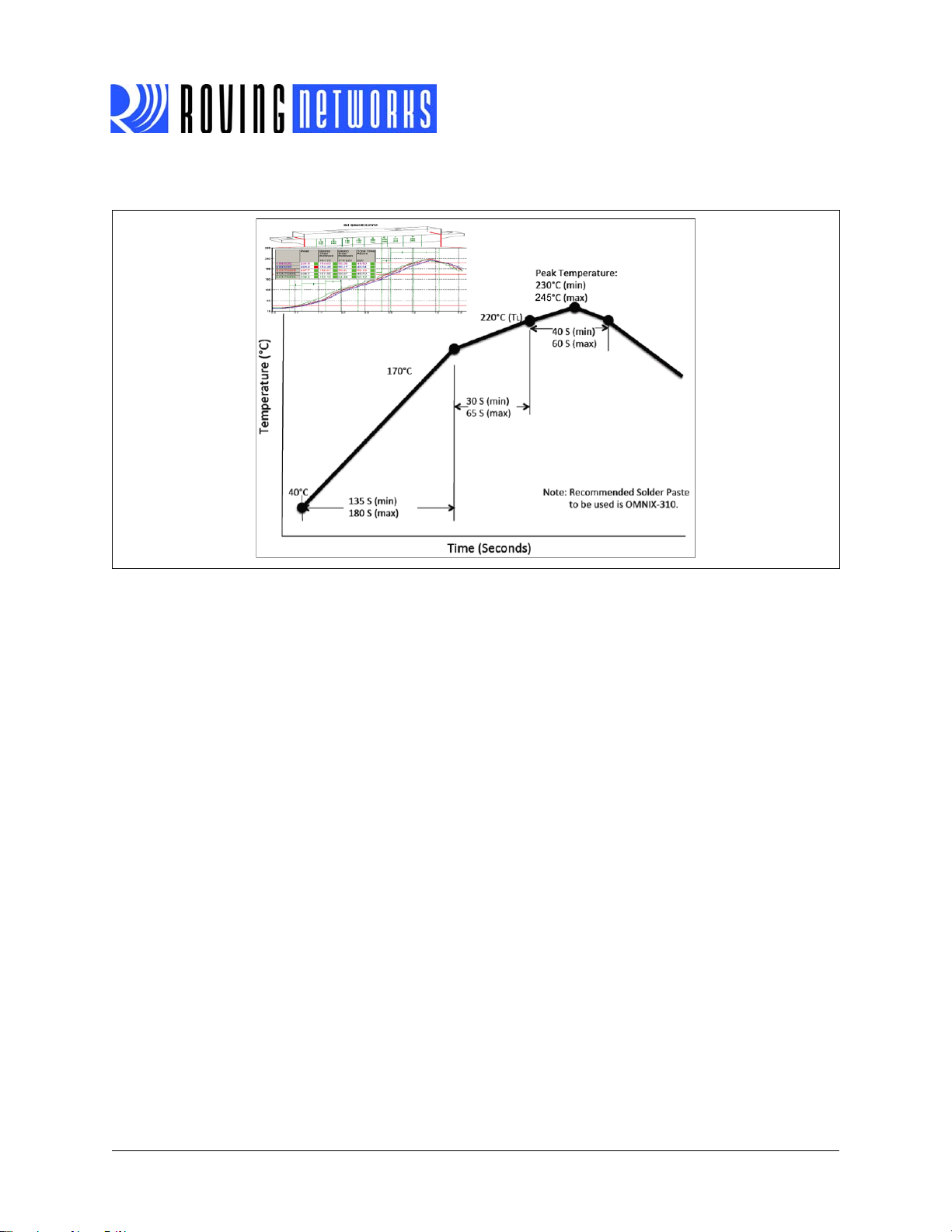
FIGURE 2-6: SOLDER REFLOW CURVE
RN52-DS
www.rovingnetworks.com Version 1.1 3/19/13 page 12
Advanced Information
Page 13

RN52-DS
VBUS
VBUS
RESET
18
3V3O UT
16
USBDP
14
USBDM
15
GND
17
CBUS210CBUS1
21
VCCIO
1
CBUS311CBUS4
9
CBUS0
22
GND
20
RI3DCD7DSR6DTR31CTS8RTS32RXD2TXD
30
VCC
19
OSCI
27
OSCO
28
AGND
2
4
TEST
26
GND
4
THPAD
33
FT232RQ
U1
GND5D+3D-2VBUS
1
MTAB
6
USB Mini B / CSR UART
J1
12345
6
J4
SPI MASTER
SPI_MI SO
SPI_MOSI
SPI_SCK
SPI_SS
3.3V
UART_RX
UART_TX
UART_CTS
UART_RTS
Vin
1
GND
2
Vout
3
Tab
4
TC1262-3.3V U2
1uF
C6
1uF
C7
VBUS 3.3V
100nFC3100nF
C1
100nF
C2
Blue LED
D3
Red LED
D2
S2
Vol Down
S3
Play / Pause
S6
Next
S1
Prev
S4
Vol Up
BTN_VOL UP
BTN_VOL DOWN
BTN_NEXT
BTN_PL AY
BTN_PREVI OUS
47R
R8
470
R9
3.3V
GND5D+3D-2VBUS
1
MTAB
6
USB Mini B / RSVD USB
J2
GPIO45GPIO5
6
GPIO127GPIO138GPIO119GPIO10
10
GPIO9
11
USBD-
12
USBD+
13
UART_RTS
14
UART_CTS
15
UART_TX
16
PCM_CL K
26
SPI_SS28SPI_MISO29SPI_SCK
30
PCM_IN
23
VDD
22
LED033MIC_BIAS34MIC_L+35MIC_R+36MIC_L-37MIC_R-
38
PCM_OUT
24
GPIO7
19
PCM_SY NC
25
SPI_MOSI31LED1
32
PWRE N
21
GPIO6
20
UART_RX
17
AIO0
4
GPIO2
3
AGND39SPKR_R-
40
GND
1
GND
18
GND
27
GND
44
GPIO3
2
SPKR_L-
41
GND
50
GND
49
GND
48
GND
47
GND
46
GND
45
SPKR_R+42SPKR_L +
43
M1
RN52 Module
PIO7
PIO6
LED0
LED1
LED0
LED1
VBUS
USBD-
USBD+
SPI_MI SO
SPI_MOSI
SPI_SCK
SPI_SS
3.3V
SPKR_R-
SPKR_L -
SPKR_R+
SPKR_L +
S5
Wake
3.3V
PCM_CLK
PCM_SYNC
PCM_OUT
PCM_IN
SPKR_R-
SPKR_L -
SPKR_R+
SPKR_L +
VBUS
47k
R2
22k
R1
PIO3
1uF
C21
1uF
C22
1uF
C13
1uF
C14
1uF
C12
2k2
R7
2k2
R6
47nFC847nF
C10
47nF
C11
47nF
C9
MIC_L
MIC_R
1uF
C18
22k
R17
22k
R15
47k
R11
22k
R13
47k
R14
47k
R10
47k
R16
22k
R12
1 2
3 4
5 6
7 8
9 10
11 12
13 14
15 16
J3
EXT Connector
PCM_CL K
PCM_SYNC
PCM_OUT
PCM_I N
3.3V
IN1+3IN1-
2
Vo2
9
BYPASS4IN2-8IN2+
7
SHUTDOWN
6
GND
5
VDD
10
Vo1
1
PAD
11
U4
TPA6112
100uF
C23
100uF
C20
100uF
C17
100uF
C19
10uF
C15
100nF
C16
MBR120
D1
10nF
C4
VBUS
PIO9
3.3V
BTN_VOLDOWN
BTN_PREVIOUS
BTN_PLAY
BTN_NEXT
BTN_VOLUP
PIO2
PIO6
PIO7
1
2
J8
MICL
1
2
J6
MICR
MIC_L
MIC_R
1
2
J11
Battery
VBUS
1234567891011
12
J10
1 2
3 4
5 6
7 8
9 10
J7
PIO4
PWREN
PWREN
SPKR_R-
SPKR_L -
SPKR_R+
SPKR_L +
MIC_BI AS
MIC_L +
MIC_R+
MIC_L -
MIC_R-
MIC_ L +
MIC_R+
MIC_ L -
MIC_R-
MIC_B I AS
AI O0
UART_RX
UART_TX
UART_CTS
UART_RTS
USBD-
USBD+
BTN_VOLUP
BTN_VOLDOWN
BTN_NEXT
BTN_PLAY
BTN_PREVIOUS
PIO3
PIO9
PIO2
PIO4
AI O0
MIC_L +
MIC_R+
MIC_L -
MIC_R-
MIC_BI AS
35421
J5
Mic
35421
J9
Headphones
2k2R70
UART_RX
UART_TX
Device
Firmware
Update
2.6 Typical Application Schematic
Figure 2-7 shows a typical application circuit with LDO,
stereo audio/microphone PA, USB/UART, AVRCP
switches, and LED0/LED1.
FIGURE 2-7: TYPICAL APPLICATION CIRCUIT FOR A2DP AUDIO STREAMING & AVRCP
REMOTE CONTROL
www.rovingnetworks.com Version 1.1 3/19/13 page 13
Advanced Information
Page 14

RN52-DS
3.0 REGULATORY APPROVAL
This section outlines the regulatory information for the
RN52 module for the following countries:
• United States
• Canada
• Europe
• Australia
• New Zealand
3.1 United States
The RN52 module has received Federal Communications Commission (FCC) CFR47 Telecommunications,
Part 15 Subpart C “Intentional Radiators” modular
approval in accordance with Part 15.212 Modular
Transmitter approval. Modular approval allows the end
user to integrate the RN52 module into a finished product without obtaining subsequent and separate FCC
approvals for intentional radiation, provided no
changes or modifications are made to the module circuitry. Changes or modifications could void the user’s
authority to operate the equipment. The end user must
comply with all of the instructions provided by the
Grantee, which indicate installation and/or operating
conditions necessary for compliance.
The finished product is required to comply with all applicable FCC equipment authorizations regulations,
requirements and equipment functions not associated
with the transmitter module portion. For example, compliance must be demonstrated to regulations for other
transmitter components within the host product; to
requirements for unintentional radiators (Part 15 Subpart B “Unintentional Radiators”), such as digital
devices, computer peripherals, radio receivers, etc.;
and to additional authorization requirements for the
non-transmitter functions on the transmitter module
(i.e., Verification, or Declaration of Conformity) (e.g.,
transmitter modules may also contain digital logic functions) as appropriate.
3.1.1 LABELING AND USER INFORMATION REQUIREMENTS
The RN52 module has been labeled with its own FCC
ID number, and if the FCC ID is not visible when the
module is installed inside another device, then the outside of the finished product into which the module is
installed must also display a label referring to the
enclosed module. This exterior label can use wording
as follows:
Contains Transmitter Module FCC ID: T9J-RN52
or
Contains FCC ID: T9J-RN52
This device complies with Part 15 of the FCC Rules.
Operation is subject to the following two conditions:
(1) this device may not cause harmful interference,
and (2) this device must accept any interference
received, including interference that may cause
undesired operation
A user’s manual for the product should include the following statement:
This equipment has been tested and found to comply
with the limits for a Class B digital device, pursuant to
part 15 of the FCC Rules. These limits are designed
to provide reasonable protection against harmful
interference in a residential installation. This equipment generates, uses and can radiate radio frequency energy, and if not installed and used in
accordance with the instructions, may cause harmful
interference to radio communications. However,
there is no guarantee that interference will not occur
in a particular installation. If this equipment does
cause harmful interference to radio or television
reception, which can be determined by turning the
equipment off and on, the user is encouraged to try to
correct the interference by one or more of the following measures:
• Reorient or relocate the receiving antenna.
• Increase the separation between the equipment
and receiver.
• Connect the equipment into an outlet on a circuit
different from that to which the receiver is connected.
• Consult the dealer or an experienced radio/TV
technician for help.
Additional information on labeling and user information
requirements for Part 15 devices can be found in KDB
Publication 784748 available at the FCC Office of Engineering and Technology (OET) Laboratory Division
Knowledge Database (KDB) http://apps.fcc.gov/oetcf/
kdb/index.cfm.
3.1.2 RF EXPOSURE
All transmitters regulated by FCC must comply with RF
exposure requirements. OET Bulletin 65, Evaluating
Compliance with FCC Guidelines for Human Exposure
www.rovingnetworks.com Version 1.1 3/19/13 page 14
Advanced Information
Page 15

RN52-DS
to Radio Frequency Electromagnetic Fields, provides
assistance in determining whether proposed or existing
transmitting facilities, operations or devices comply
with limits for human exposure to Radio Frequency
(RF) fields adopted by the Federal Communications
Commission (FCC). The bulletin offers guidelines and
suggestions for evaluating compliance.
If appropriate, compliance with exposure guidelines for
mobile and unlicensed devices can be accomplished
by the use of warning labels and by providing users
with information concerning minimum separation distances from transmitting structures and proper installation of antennas.
The following statement must be included as a CAUTION statement in manuals and OEM products to alert
users of FCC RF exposure compliance:
To satisfy FCC RF Exposure requirements for mobile
and base station transmission devices, a separation
distance of 20 cm or more should be maintained
between the antenna of this device and persons during operation. To ensure compliance, operation at
closer than this distance is not recommended.
The antenna(s) used for this transmitter must not be
co-located or operating in conjunction with any other
antenna or transmitter.
If the RN52 module is used in a portable application
(i.e., the antenna is less than 20 cm from persons during operation), the integrator is responsible for performing Specific Absorption Rate (SAR) testing in
accordance with FCC rules 2.1091.
3.1.3 HELPFUL WEB SITES
Federal Communications Commission (FCC):
http://www.fcc.gov
FCC Office of Engineering and Technology (OET) Laboratory Division Knowledge Database (KDB):
http://apps.fcc.gov/oetcf/kdb/index.cfm
3.2 Canada
The RN52 module has been certified for use in Canada
under Industry Canada (IC) Radio Standards Specification (RSS) RSS-210 and RSSGen. Modular approval
permits the installation of a module in a host device
without the need to recertify the device.
3.2.1 LABELING AND USER INFORMATION REQUIREMENTS
Labeling Requirements for the Host Device (from Section 3.2.1, RSS-Gen, Issue 3, December 2010): The
host device shall be properly labeled to identify the
module within the host device.
The Industry Canada certification label of a module
shall be clearly visible at all times when installed in the
host device, otherwise the host device must be labeled
to display the Industry Canada certification number of
the module, preceded by the words “Contains transmitter module”, or the word “Contains”, or similar wording
expressing the same meaning, as follows:
Contains transmitter module IC: 6514A-RN52
User Manual Notice for License-Exempt Radio Apparatus (from Section 7.1.3 RSS-Gen, Issue 3, December
2010): User manuals for license-exempt radio apparatus shall contain the following or equivalent notice in a
conspicuous location in the user manual or alternatively on the device or both:
This device complies with Industry Canada licenseexempt RSS standard(s). Operation is subject to the
following two conditions: (1) this device may not
cause interference, and (2) this device must accept
any interference, including interference that may
cause undesired operation of the device.
Le présent appareil est conforme aux CNR d'Industrie Canada applicables aux appareils radio exempts
de licence. L'exploitation est autorisée aux deux conditions suivantes: (1) l'appareil ne doit pas produire
de brouillage, et (2) l'utilisateur de l'appareil doit
accepter tout brouillage radioélectrique subi, même
si le brouillage est susceptible d'en compromettre le
fonctionnement.
Transmitter Antenna (from Section 7.1.2 RSS-Gen,
Issue 3, December 2010): User manuals for transmitters shall display the following notice in a conspicuous
location:
Under Industry Canada regulations, this radio transmitter may only operate using an antenna of a type
and maximum (or lesser) gain approved for the transmitter by Industry Canada. To reduce potential radio
interference to other users, the antenna type and its
gain should be so chosen that the equivalent isotropically radiated power (e.i.r.p.) is not more than that
necessary for successful communication.
Conformément à la réglementation d'Industrie Canada, le présent émetteur radio peut fonctionner avec
une antenne d'un type et d'un gain maximal (ou
inférieur) approuvé pour l'émetteur par Industrie Canada. Dans le but de réduire les risques de brouillage
radioélectrique à l'intention des autres utilisateurs, il
faut choisir le type d'antenne et son gain de sorte
que la puissance isotrope rayonnée équivalente
(p.i.r.e.) ne dépasse pas l'intensité nécessaire à
l'établissement d'une communication satisfaisante.
www.rovingnetworks.com Version 1.1 3/19/13 page 15
Advanced Information
Page 16

RN52-DS
The above notice may be affixed to the device instead
of displayed in the user manual.
3.2.2 HELPFUL WEB SITES
Industry Canada: http://www.ic.gc.ca/
3.3 Europe
The RN52 module is an R&TTE Directive assessed
radio module that is CE marked and has been manufactured and tested with the intention of being integrated into a final product.
The RN52 module has been tested to R&TTE Directive
1999/5/EC Essential Requirements for Health and
Safety (Article (3.1(a)), Electromagnetic Compatibility
(EMC) (Article 3.1(b)), and Radio (Article 3.2) and are
summarized in Table 3-1: European Compliance Testing. A Notified Body Opinion has also been issued. All
test reports are available on the RN52 product web
page at http://www.microchip.com.
The R&TTE Compliance Association provides guidance on modular devices in document Technical Guidance Note 01 available at http://www.rtteca.com/html/
download_area.htm.
Note: To maintain conformance to the testing
listed in Ta bl e 3 -1 , the module shall be
installed in accordance with the installation instructions in this data sheet and
shall not be modified.
When integrating a radio module into a
completed product the integrator
becomes the manufacturer of the final
product and is therefore responsible for
demonstrating compliance of the final
product with the essential requirements of
the R&TTE Directive.
3.3.2 ANTENNA REQUIREMENTS
From R&TTE Compliance Association document Technical Guidance Note 01:
Provided the integrator installing an assessed
radio module with an integral or specific antenna
and installed in conformance with the radio module manufacturer’s installation instructions
requires no further evaluation under Article 3.2
of the R&TTE Directive and does not require further involvement of an R&TTE Directive Notified
Body for the final product. [Section 2.2.4]
3.3.3 HELPFUL WEB SITES
A document that can be used as a starting point in
understanding the use of Short Range Devices (SRD)
in Europe is the European Radio Communications
Committee (ERC) Recommendation 70-03 E, which
can be downloaded from the European Radio Communications Office (ERO) at: http://www.ero.dk/.
Additional helpful web sites are:
• Radio and Telecommunications Terminal Equipment (R&TTE):
http://ec.europa.eu/enterprise/rtte/index_en.htm
• European Conference of Postal and Telecommunications Administrations (CEPT):
http://www.cept.org
• European Telecommunications Standards Institute (ETSI):
http://www.etsi.org
• European Radio Communications Office (ERO):
http://www.ero.dk
• The Radio and Telecommunications Terminal
Equipment Compliance Association (R&TTE CA):
http://www.rtteca.com/
3.3.1 LABELING AND USER INFORMATION REQUIREMENTS
The label on the final product which contains the RN52
module must follow CE marking requirements. The
R&TTE Compliance Association Technical Guidance
Note 01 provides guidance on final product CE marking.
www.rovingnetworks.com Version 1.1 3/19/13 page 16
Advanced Information
Page 17

RN52-DS
TABLE 3-1: EUROPEAN COMPLIANCE TESTING
Certification Standards Article Laboratory Report Number Date
Safety EN 60950-1:2006+A11:2009+A1:2010 (3.1(a))
Health EN 50371:2002-03
EMC EN 301 489-1 V1.8.1 (2008-04) (3.1(b))
EN 301 489-17 V2.1.1 (2009-05)
Radio EN 300 328 V1.7.1 (2006-10) (3.2)
Notified Body
Opinion
DoC
3.4 Australia
The Australia radio regulations do not provide a modular approval policy similar to the United States (FCC)
and Canada (IC). However, RN52 module RF transmitter test reports can be used in part to demonstrate compliance in accordance with ACMA Radio
communications “Short Range Devices” Standard
2004 (The Short Range Devices standard calls up the
AS/NZS 4268:2008 industry standard). The RN52
module test reports can be used as part of the product
certification and compliance folder. For more information on the RF transmitter test reports, contact Microchip Technology Australia sales office.
To meet overall Australian final product compliance, the
developer must construct a compliance folder containing all relevant compliance test reports e.g. RF, EMC,
electrical safety and DoC (Declaration of Conformity)
etc. It is the responsibility of the integrator to know what
is required in the compliance folder for ACMA compliance. All test reports are available on the RN52 product
web page at http://www.microchip.com. For more information on Australia compliance, refer to the Australian
Communications and Media Authority web site
http://www.acma.gov.au/.
3.4.1 HELPFUL WEB SITES
The Australian Communications and Media Authority:
www.acma.gov.au/.
as part of the product certification and compliance
folder. All test reports are available on the RN52 product web page at http://www.microchip.com. For more
information on the RF transmitter test reports, contact
Microchip Technology sales office.
Information on the New Zealand short range devices
license can be found in the following web links:
http://www.rsm.govt.nz/cms/licensees/types-oflicence/general-user-licences/short-range-devices
and
http://www.rsm.govt.nz/cms/policy-and-planning/spectrum-policy-overview/legislation/gazette-notices/product-compliance/radiocommunications-radiostandardsnotice-2010.
To meet overall New Zealand final product compliance,
the developer must construct a compliance folder containing all relevant compliance test reports e.g. RF,
EMC, electrical safety and DoC (Declaration of Conformity) etc. It is the responsibility of the developer to
know what is required in the compliance folder for New
Zealand Radio communications. For more information
on New Zealand compliance, refer to the web site
http://www.rsm.govt.nz/.
3.5.1 HELPFUL WEB SITES
Radio Spectrum Ministry of Economic Development:
http://www.rsm.govt.nz/.
3.5 New Zealand
The New Zealand radio regulations do not provide a
modular approval policy similar to the United States
(FCC) and Canada (IC). However, RN52 module RF
transmitter test reports can be used in part to demonstrate compliance against the New Zealand “General
User Radio License for Short Range Devices”. New
Zealand Radio communications (Radio Standards)
Notice 2010 calls up the AS / NZS 4268:2008 industry
standard. The RN52 module test reports can be used
www.rovingnetworks.com Version 1.1 3/19/13 page 17
Advanced Information
Page 18

4.0 ORDERING INFORMATION
Ta bl e 4 - 1 provides ordering information for the RN52
module.
TABLE 4-1: ORDERING INFORMATION
Part Number Description
RN52-I/RM Standard application firmware (A2DP/AVRCP/SPP) master and slave).
For other configurations, contact Roving Networks directly.
Go to http://www.rovingnetworks.com for current pricing and a list of distributors carrying Roving Networks
products.
5.0 DOCUMENT REVISION
HISTORY
5.1 Version 1.1
RN52-DS
• Updated pin information.
• Added more details on RN52 layout o host PCB.
5.2 Version 1.0
Initial release.
This device has not been authorized
as required by the rules of the Federal
Communications Commission. This
device is not, and may not be, offered
for sale or lease, or sold or leased,
until authorization is obtained.
Copyright © 2013 Roving Networks. All rights reserved. Roving Networks
is a registered trademark of Roving Networks. Apple Inc., iPhone, iPad,
iTunes, Made for iPhone are registered trademarks of Apple Computer.
Roving Networks reserves the right to make corrections, modifications,
and other changes to its products, documentation and services at any
time. Customers should obtain the latest relevant information before placing orders and should verify that such information is current and complete.
Roving Networks assumes no liability for applications assistance or customer’s product design. Customers are responsible for their products and
applications that use Roving Networks components. To minimize customer product risks, customers should provide adequate design and operating safeguards.
Roving Networks, Inc.
102 Cooper Court
Los Gatos, CA 95032
+1 (408) 395-5300
www.rovingnetworks.com
www.rovingnetworks.com Version 1.1 3/19/13 page 18
Roving Networks products are not authorized for use in safety-critical
applications (such as life support) where a failure of the Roving Networks
product would reasonably be expected to cause severe personal injury or
death, unless officers of the parties have executed an agreement specifically governing such use.
Advanced Information
 Loading...