

Page 1
PL360
Embedded USI
G3-PLC Stack
PHY + PLC Transceiver
SAM4C
( ITU-T G.9903 )
( IEEE 802.15.4 )
( IETF RFC 4944 )
Adaptation Layer
MAC Layer
PAL Layer
sniffer_if
phy_if
mac_if
adp_if
app_if
Host Controller
PLC
USER APPLICATION
PL360
SPI
PLATFORM
IPv6 STACK
Detect
Interrupt
Carrier
PL360 Host Controller
Introduction
The PL360 is a multi-protocol modem for the Power Line Communication (PLC) device, implementing a
very flexible architecture and allowing the implementation of standard and customized PLC solutions. It
has been conceived to be bundled with an external Microchip MCU, which downloads the corresponding
PLC firmware and controls the operation of the PL360 device.
The purpose of the PL360 Host Controller is to provide the external microcontroller a way to control the
PL360 device and offer upper layers an easy way to get access to PLC communication.
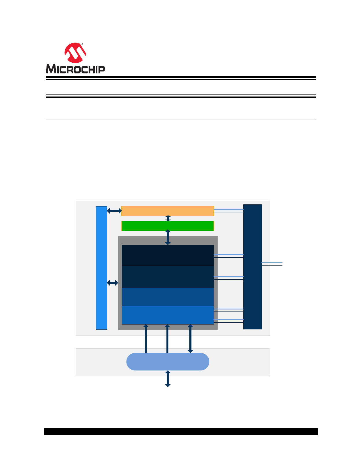
As an example of the PLC system, the figure below shows the system architecture for G3 protocol based
on a PL360 device being controlled by a SAM4C MCU.
Figure 1. G3 System Architecture
The aim of this document is to clarify and detail the user interface of the PL360 Host Controller.
© 2018 Microchip Technology Inc.
User Guide
50002738B-page 1
Page 2

Features
• Compliant with PRIME 1.3 Physical Layer
• Compliant with PRIME 1.4 Physical Layer
• Compliant with G3 Physical Layer
• SPI Interface
• Secure Boot Option
PL360
© 2018 Microchip Technology Inc.
User Guide
50002738B-page 2
Page 3

Table of Contents
Introduction......................................................................................................................1
Features.......................................................................................................................... 2
1. PL360 Host Controller Architecture........................................................................... 5
1.1. PL360 Host Controller File Structure............................................................................................5
1.2. PLC Application Interface (API)....................................................................................................6
1.3. PLC Stack Wrapper......................................................................................................................6
1.4. Add-ons........................................................................................................................................7
1.5. Bootloader....................................................................................................................................7
1.6. Hardware Abstraction Layer (HAL).............................................................................................. 7
2. PL360 System Architecture....................................................................................... 8
2.1. Block Diagram.............................................................................................................................. 8
2.2. Bootloader....................................................................................................................................8
2.3. PL360 Memory............................................................................................................................. 9
2.4. PL360 Drivers...............................................................................................................................9
2.5. PHY PLC Service......................................................................................................................... 9
2.6. PHY Host Application................................................................................................................. 10
3. Brief about ASF........................................................................................................11
4. Initialization Example...............................................................................................12
4.1. Init Controller Descriptor.............................................................................................................12
4.2. Set Controller Callbacks.............................................................................................................12
4.3. Enable Controller........................................................................................................................13
4.4. PLC Event Handling................................................................................................................... 13
4.5. Code Example............................................................................................................................14
5. Configuration........................................................................................................... 15
5.1. Configure Application................................................................................................................. 15
5.2. Configure Coupling Parameters................................................................................................. 15
5.3. Configure Secure Mode............................................................................................................. 16
6. Host Interface Management.................................................................................... 17
6.1. Message Transmission...............................................................................................................17
6.2. Message Reception....................................................................................................................17
7. SPI Protocol.............................................................................................................18
7.1. Boot Command Format.............................................................................................................. 18
7.2. Boot Response Format.............................................................................................................. 18
7.3. Firmware Command Format...................................................................................................... 19
7.4. Firmware Response Format.......................................................................................................20
7.5. Firmware Data Memory Regions................................................................................................20
7.6. Message Flow for Basic Transactions........................................................................................22
© 2018 Microchip Technology Inc.
User Guide
50002738B-page 3
Page 4

8. Example Applications.............................................................................................. 33
8.1. PHY Examples........................................................................................................................... 33
9. Supported Platforms................................................................................................35
9.1. Supported MCU Families........................................................................................................... 35
9.2. Supported Transceivers............................................................................................................. 35
9.3. Supported Boards...................................................................................................................... 35
9.4. Platform Porting..........................................................................................................................35
10. Abbreviations...........................................................................................................36
11. References.............................................................................................................. 38
12. Appendix A: PL360 Host Controller API..................................................................39
12.1. Common PHY API......................................................................................................................39
12.2. G3 PHY API............................................................................................................................... 42
12.3. PRIME PHY SAP....................................................................................................................... 59
13. Appendix B: ZC Offset Configuration...................................................................... 74
PL360
14. Revision History.......................................................................................................75
14.1. Rev A – 03/2018.........................................................................................................................75
14.2. Rev B - 10/2018......................................................................................................................... 75
The Microchip Web Site................................................................................................ 76
Customer Change Notification Service..........................................................................76
Customer Support......................................................................................................... 76
Microchip Devices Code Protection Feature................................................................. 76
Legal Notice...................................................................................................................77
Trademarks................................................................................................................... 77
Quality Management System Certified by DNV.............................................................78
Worldwide Sales and Service........................................................................................79
© 2018 Microchip Technology Inc.
User Guide
50002738B-page 4
Page 5

1. PL360 Host Controller Architecture
HOST MCU
PLC Appli cation
PLC Application Interface API
Bootloader PLC Stack Wrapper Add-ons
PL360 Host Controller
Hardware Abstracion Layer
The PL360 Host Controller is a C source code component which provides the host MCU application
access to the API of the Power Line Communications PHY layer running in the PL360 device. Figure 1-1
shows the architecture of the software which runs on the host MCU. The components of the PL360 Host
Controller are described in the following subsections.
Figure 1-1. PL360 Host Controller Architecture
PL360
PL360 Host Controller Architecture
1.1 PL360 Host Controller File Structure
The PL360 Host Controller is provided as a component of ASF (Atmel Software Framework). The image
below shows the location of the main files of the PL360 Host Controller Software. Different blocks provide
different features. The next subsections describe the purpose of each block.
© 2018 Microchip Technology Inc.
User Guide
50002738B-page 5
Page 6
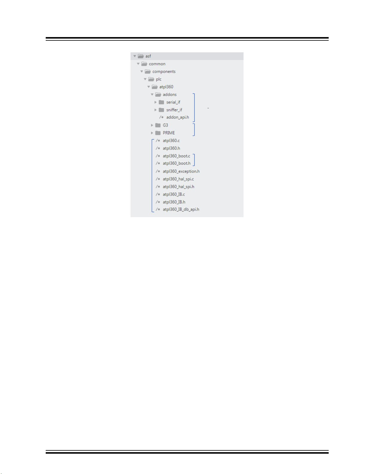
Figure 1-2. PL360 Host Controller File Structure
Add
on s
PLC Sta ck W
r
a
pper
Bootl oader
API
&
HAL
PL360
PL360 Host Controller Architecture
1.2 PLC Application Interface (API)
This module provides an interface to the application for all PLC operations.
This API includes the following services:
• Set custom hardware interface
• Manage Bootloader process of the PL360 device
• Manage external configuration of the PL360 device
• Enable / Disable PLC interface
• Enable / Disable secure mode
• Enable / Disable add-on module
This interface is defined in file atpl360.h and some of these services can be configured in file
conf_atpl360.h (see 5.1 Configure Application).
1.3 PLC Stack Wrapper
This module provides an interface compliant with the specific PLC communication stack, G3 or PRIME. It
includes all declarations and definitions relative to the specific communication stack.
The main function of this module is to parse/serialize frames between SPI protocol and API functions in
order to manage information from/to upper layers. It also provides a configuration function to set some
hardware- specific parameters during the initialization process.
For further details, please refer to atpl360_comm.h header file.
© 2018 Microchip Technology Inc.
User Guide
50002738B-page 6
Page 7

1.4 Add-ons
This module is responsible for providing compatibility with Microchip PLC tools. Its main function is to
pack/unpack frames so that they can be used by each PLC tool.
There are two add-ons available per PLC communication stack: one to connect with the Microchip PLC
Sniffer PC tool, and another one to connect with the Microchip PLC PHY Tester PC tool.
1.5 Bootloader
The PL360 device is a RAM-based device, so it is required to transfer the binary code to the device after
each reset. The main purpose of this module is to manage the download process.
During the bootloading, the integrity of the SPI communication between the PL360 Host Controller and
the PL360 device is checked in each SPI transaction. If the SPI header does not match the expected
information, the PL360 Host Controller resets the PL360 device and the bootloader downloads the binary
code to the device again. The PL360 Host Controller tries this download process up to three times and
reports a critical failure to upper layers after the last unsuccessful download process.
There are two modes of operation for the bootloader: Normal mode or Secure mode.
PL360
PL360 Host Controller Architecture
The following points should be taken into account in order to enable the Secure Boot mode:
• It is mandatory to include specific metadata in the binary file before downloading it to the PL360
device, such as number of blocks to decypher, init vector and signature. A Microchip Python script
is provided in PLC PHY Workspace as an example about how to include this metadata information
in the binary file
• It is needed to define ATPL360_SEC_BOOT_MODE in conf_atpl360.h file, and make sure that
__ATPL360B__ is defined as symbol in project properties
For further details, please check the bootloader commands defined in atpl360_hal_spi.h header file.
1.6 Hardware Abstraction Layer (HAL)
The Hardware Abstraction Layer provides full hardware compatibility with the host device.
There are four hardware peripherals that depend on customer platform/implementation:
• Access to SPI peripheral
• Access to interrupt system
• Access to delay system
• Access to carrier detect line
For further details, please refer to section 4. Initialization Example.
© 2018 Microchip Technology Inc.
User Guide
50002738B-page 7
Page 8

2. PL360 System Architecture
PL360 SoC
PHY Host Application
PHY
UTILS
TX
Chain
Coupling
PHY PLC Service
Application Interface (PHY API)
Bootloader
DACC
PL360 Drivers
ADCC SPI XDMAC XCORR PIO CRC
WDT SPU APMC
RX
Chain
Shared
Memory
Host
Interface
Zero
Cross
Program
Memory
Data
Memory
2.1 Block Diagram
Figure 2-1 shows the PL360 system architecture of the embedded firmware. The PL360 device has an
embedded Cortex M7 CPU to run the PLC firmware. This firmware can either implement the G3 or the
PRIME Physical layer depending on what has been loaded by the PL360 Host Controller. The
components of the system are described in the following subsections.
Figure 2-1. PL360 Embedded Firmware Architecture
PL360
PL360 System Architecture
2.2 Bootloader
The bootloader is an Internal Peripheral (IP) designed to load the program from an external master into
the instruction memory of the Cortex M7. This IP can access instruction memory, data memory and
peripheral registers.
For further information, please refer to the PL360 datasheet.
© 2018 Microchip Technology Inc.
User Guide
50002738B-page 8
Page 9

2.3 PL360 Memory
There are two memory configurations controlled via MEM_CONFIG bit. In the firmware loading process,
the appropriate memory configuration is established by the PL360 Host Controller according to the
firmware requisites.
MEM_CONFIG Program memory Data memory
0 128 KBytes 64 KBytes
1 96 KBytes 96 KBytes
The PL360 Host Controller code provided by Microchip sets MEM_CONFIG to 1 by default.
For further information, please refer to the PL360 datasheet.
2.4 PL360 Drivers
Each driver is responsible for managing a hardware peripheral:
• WDT: Watchdog system
• SPU: Signal Processing Unit
• APMC: Advanced Power Management Controller
• DACC: Digital to Analog Converter Controller
• ADCC: Analog to Digital Converter Controller
• SPI: Serial Peripheral Interface
• XDMAC: DMA Controller
• XCORR: Correlator
• PIO: Parallel Input/Output Controller
• CRC: Cyclic Redundancy Check
PL360
PL360 System Architecture
2.5 PHY PLC Service
There are several blocks in the PHY PLC service:
• Application Interface: The API provides a set of functions to access the physical medium and
different parameters relative to each communication stack
• Host Interface: This block is in charge of managing the communication with the PL360 Host
Controller through SPI. It is responsible for parsing/serializing the SPI data, managing PLC data
regions and providing control on PLC Interruption PIO
• Coupling: This block contains the hardware configuration associated to the reference design
provided by Microchip. If a customer needs to change this configuration to adapt it to its own
design, please refer to the 5.2 Configure Coupling Parameters chapter
• TX Chain: The TX chain is responsible for handling messages from upper layers (passed through
the API) to the physical output. This block controls all drivers relative to transmission and adapts
signal parameters in order to use functionalities of the transmission chain PHY Utils block:
convolutional encoder, scrambler, interleaver, modulator, IFFT and interpolator. Also, it handles the
result of the transmission in order to report it to upper layers through the API
• RX Chain: The RX chain is responsible for handling messages from the physical input to upper
layers (passed through the API). This block checks if the PLC signal is present on the PLC
© 2018 Microchip Technology Inc.
User Guide
50002738B-page 9
Page 10

medium, synchronizes with this PLC signal and drives the signal through functionalities of the
reception chain in the PHY Utils block: decimator, FFT, demodulator, deinterleaver, descrambler
and Viterbi block. Also, it builds the complete message and reports it to upper layers through the
API
• Shared Memory: This block defines the structure of the data memory to avoid collisions between
TX and RX chains
• Zero Cross: The Zero Cross is responsible for calculating the last Zero Cross value and providing it
to the PLC communication stack in use. For further information, please refer to 13. Appendix B: ZC
Offset Configuration
• PHY Utils: This block contains several functionalities used by the TX/RX chains
2.6 PHY Host Application
The PHY Host Application is responsible for running the main application of the PL360 device. It is in
charge of initializing the hardware and clock systems, checking the watchdog timer and managing the
PL360 PLC service described in the previous chapter.
PL360
PL360 System Architecture
© 2018 Microchip Technology Inc.
User Guide
50002738B-page 10
Page 11

3. Brief about ASF
The Advanced Software Framework (ASF) is a MCU software library providing a large collection of
embedded software for Atmel flash MCUs: megaAVR, AVR XMEGA, AVR UC3 and SAM devices.
For details on ASF please refer to Advanced Software Framework documentation:
• Advanced Software Framework - Website
• [PDF] Atmel AVR4029: Atmel Software Framework - Getting Started
• [PDF] Atmel AVR4030: Atmel Software Framework - Reference Manual
PL360
Brief about ASF
© 2018 Microchip Technology Inc.
User Guide
50002738B-page 11
Page 12

4. Initialization Example
CAUTION
This chapter aims to explain the different steps required during the initialization phase of the system. After
powering up the PL360 device, a set of initialization sequences must be executed in the correct order for
the proper operation of the PL360 device.
The steps are the following:
1. Init controller descriptor
2. Set controller callbacks
3. Enable controller
4. PL360 event handling
Failure to complete any of the these initialization steps will result in failure in the PL360 Host
Controller startup.
PL360
Initialization Example
4.1 Init Controller Descriptor
The PL360 Host Controller is initialized by calling the atpl360_init function in the API. The PL360
Host Controller initialization routine performs the following steps:
• Disable PLC interrupt and component
• Register wrapper for hardware abstraction layer (for further information, please refer to 12.1.1
Initialization Function)
• Reset the PL360 device using corresponding host MCU control GPIOs
• Configure a GPIO as an interrupt source from the PL360 device
• Initialize the SPI driver
• Register an internal event handler for the external PLC interrupt
• If an add-on is required, initialize specific add-on (configured previously). See chapter 5.1
Configure Application
• Return a descriptor to the PL360 Host Controller. This descriptor will be used to manage the PLC
communication
4.2 Set Controller Callbacks
After initializing the PL360 Host Controller, it is important to set callbacks to manage PL360 events.
The PL360 Host Controller reports PLC events using callback functions.
There are 4 callback functions.
• Data indication: Used to report a new incoming message
• Data confirm: Used to report the result of the last transmitted message
• Add-on event: Used to report that a new add-on message is ready to be sent to the PLC application
• Exception event: Used to report if an exception occurs, such as a reset of the PL360 device
© 2018 Microchip Technology Inc.
User Guide
50002738B-page 12
Page 13

4.3 Enable Controller
WARNING
The PL360 Host Controller is enabled by calling the atpl360_enable function in the API. This PL360
Host Controller routine performs the following steps:
• Disable/enable PLC interrupt and component
• Transfer the PL360 firmware to the PL360 device and validate. In case of failure, report a critical
error in host communication with the PL360 device through exception callback
4.4 PLC Event Handling
Once the controller callbacks have been set up, the PL360 Host Controller component must be enabled.
Then, the host MCU application is required to call the PL360 Host Controller API periodically to handle
events from PL360 embedded firmware.
The PL360 Host Controller API allows the host MCU application to interact with the PL360 embedded
firmware. To facilitate interaction, the PL360 Host Controller implements the host interface protocol
described in section 6. Host Interface Management. This protocol defines how to serialize and how to
handle API requests and response callbacks over the SPI bus interface.
PL360
Initialization Example
Some PL360 Host Controller APIs are synchronous function calls, whose return indicates that the
requested action is completed. However, most API functions are asynchronous. This means that when
the application calls an API to request a service, the call is non-blocking and returns immediately, usually
before the requested action is completed. When the requested action is completed, a notification is
provided in the form of a host interface protocol message from the PL360 embedded firmware to the
PL360 Host Controller, which, in turn, delivers it to the application via callback functions. Asynchronous
operation is essential when the requested service, such as a PLC message transmission, may take
significant time to complete. In general, the PL360 embedded firmware uses asynchronous events to
notify the host driver of status changes or pending data.
The PL360 device interrupts the host MCU when one or more events are pending in the PL360
embedded firmware. The host MCU application processes received data and events when the PL360
Host Controller calls the corresponding event callback function(s). In order to receive event callbacks, the
host MCU application is required to periodically call the atpl360_handle_events function in the API.
When host MCU application calls atpl360_handle_events, the PL360 Host Controller checks for
pending unhandled interrupts from the PL360 device. If no interrupt is pending, it returns immediately. If
an interrupt is pending, atpl360_handle_events function dispatches the PLC event data to the
respective registered callback. If the corresponding callback is not registered, the PLC event is discarded.
It is recommended to call this function either:
• From the main loop or from a dedicated task in the host MCU application; or,
• At least once when the host MCU application receives an interrupt from the PL360 embedded
firmware
The Host driver function atpl360_handle_events is non re-entrant. In the operating
system configuration, it is required to protect the PL360 Host Controller from re-entrance.
© 2018 Microchip Technology Inc.
User Guide
50002738B-page 13
Page 14

4.5 Code Example
The code example below shows the initialization flow as described in previous sections.
/**
* \brief Handler to receive add-on data from ATPL360.
*/
static void _handler_serial_atpl360_event(uint8_t *px_serial_data, uint16_t us_len)
{
/* customer application */
}
/**
* \brief Main code entry point.
*/
int main( void )
{
atpl360_dev_callbacks_t x_atpl360_cbs;
atpl360_hal_wrapper_t x_atpl360_hal_wrp;
uint8_t uc_ret;
/* ASF function to setup clocking. */
sysclk_init();
/* ASF library function to setup for the evaluation kit being used. */
board_init();
/* Init ATPL360 */
x_atpl360_hal_wrp.plc_init = hal_plc_init;
x_atpl360_hal_wrp.plc_reset = hal_plc_reset;
x_atpl360_hal_wrp.plc_set_handler = hal_plc_set_handler;
x_atpl360_hal_wrp.plc_send_boot_cmd = hal_plc_send_boot_cmd;
x_atpl360_hal_wrp.plc_write_read_cmd = hal_plc_send_wrrd_cmd;
x_atpl360_hal_wrp.plc_enable_int = hal_plc_enable_interrupt;
x_atpl360_hal_wrp.plc_delay = hal_plc_delay;
atpl360_init(&sx_atpl360_desc, &x_atpl360_hal_wrp);
/* Callback configuration. Set NULL as Not used */
x_atpl360_cbs.data_confirm = NULL;
x_atpl360_cbs.data_indication = NULL;
x_atpl360_cbs.exception_event = NULL;
x_atpl360_cbs.addons_event = _handler_serial_atpl360_event;
sx_atpl360_desc.set_callbacks(&x_atpl360_cbs);
/* Enable ATPL360 */
uc_ret = atpl360_enable(ATPL360_BINARY_ADDRESS, ATPL360_BINARY_LEN);
if (uc_ret == ATPL360_ERROR) {
printf("\r\nmain: atpl360_enable call error!(%d)\r\n", uc_ret);
while (1) {
}
}
while (1) {
/* Check ATPL360 pending events */
atpl360_handle_events();
}
}
PL360
Initialization Example
© 2018 Microchip Technology Inc.
User Guide
50002738B-page 14
Page 15

5. Configuration
The PL360 firmware has a set of configurable parameters that control its behavior. There is a set of
configuration APIs provided to the host MCU application to configure these parameters. The configuration
APIs are categorized according to their functionality: application, coupling parameters and secure mode.
Any parameter left unset by the host MCU application will use the default value assigned during the
initialization of the PL360 firmware.
Info: All configuration parameters described in this chapter can be found in conf_atpl360.h file.
5.1 Configure Application
The following parameters can be modified to alter the behavior of the device.
• Use add-on capabilities:
– Serial Interface: provides handling of messages to communicate with the Microchip PLC PHY
Tester PC tool and PLC Python scripts
– Sniffer Interface: provides handling of messages to communicate with the Microchip PLC
Sniffer PC tool
PL360
Configuration
Info: These add-on modules are included in the PLC PHY workspace provided by Microchip.
This workspace contains the projects to use with the Microchip PLC tools commented on
previously.
• Only in case of G3 communication stack, the frequency band can be selected depending on
customer requirements. G3 CEN-A, CEN-B and FCC bands are available using ATPL360_WB
parameter in the file conf_atpl360.h. Take into account that this configuration requires the use
of different firmware binary files in the PL360 device. For further information, please refer to 12.2.1
Bandplan Selection.
5.2 Configure Coupling Parameters
Sometimes the hardware designed by the customer hasn’t got exactly the same performance as the
reference design provided by Microchip, so it is possible that some adjustments are needed in order to
get the best performance.
For that purpose, the following parameters can be modified:
• MAX_RMS_HI_TABLE, MAX_RMS_VLO_TABLE: Coupling parameters to define RMS values in
Hi/Vlo impedance
• TH1_HI_TABLE, TH2_HI_TABLE, TH1_VLO_TABLE, TH2_VLO_TABLE: Coupling parameters
to define threshold values to check in Hi/Vlo impedance
• PREDIST_COEF_HI_TABLE, PREDIST_COEF_VLO_TABLE: Coupling parameters to define
Predistortion Coefficients in Hi/Vlo impedance
© 2018 Microchip Technology Inc.
User Guide
50002738B-page 15
Page 16

PL360
Configuration
IFFT_GAIN_HI_INI, IFFT_GAIN_VLO_INI, IFFT_GAIN_HI_MIN, IFFT_GAIN_VLO_MIN,
•
IFFT_GAIN_HI_MAX, IFFT_GAIN_VLO_MAX : Coupling parameters to define IFFT Gain in Hi/Vlo
impedance
• DACC_CFG_TABLE: Coupling parameters to define DACC behavior
Tip: Microchip provides a specific tool called PHY Calibration Tool with the purpose of helping
customers calculate the best values for all coupling parameters depending on their own
hardware design.
During startup, the PL360 Host Controller verifies that the firmware is running in the PL360 device and
sets custom coupling parameters through the atpl360_comm_set_coup_cfg function in the API,
which should be adapted by customers depending on their hardware requirements. The PL360 Host
Controller calls this function after any unexpected reset of the PL360 device.
Tip: To apply a customized coupling configuration, ATPL360_CFG_COUP_ENABLE must be
uncommented in conf_atpl360.h file.
5.3 Configure Secure Mode
For further information, please contact the Microchip support team.
© 2018 Microchip Technology Inc.
User Guide
50002738B-page 16
Page 17
6. Host Interface Management
The PL360 Host Controller services are divided in two categories: synchronous and asynchronous
services. See 4.4 PLC Event Handling.
Most of the services implemented by the PL360 Host Controller are asynchronous.
The synchronous service is only used in the get_config function in order to get specific internal
parameters relative to the communication stack.
When a function from the API is called, a sequence of actions is activated to format the request and to
arrange to transfer it to the PL360 device through the SPI protocol.
When an asynchronous event occurs, the PL360 Host Controller handles the PLC interrupt, checks the
events reported by the PL360 device and extracts the information relative to the notified event.
The associated callback will be invoked in the next call to atpl360_handle_events function.
6.1 Message Transmission
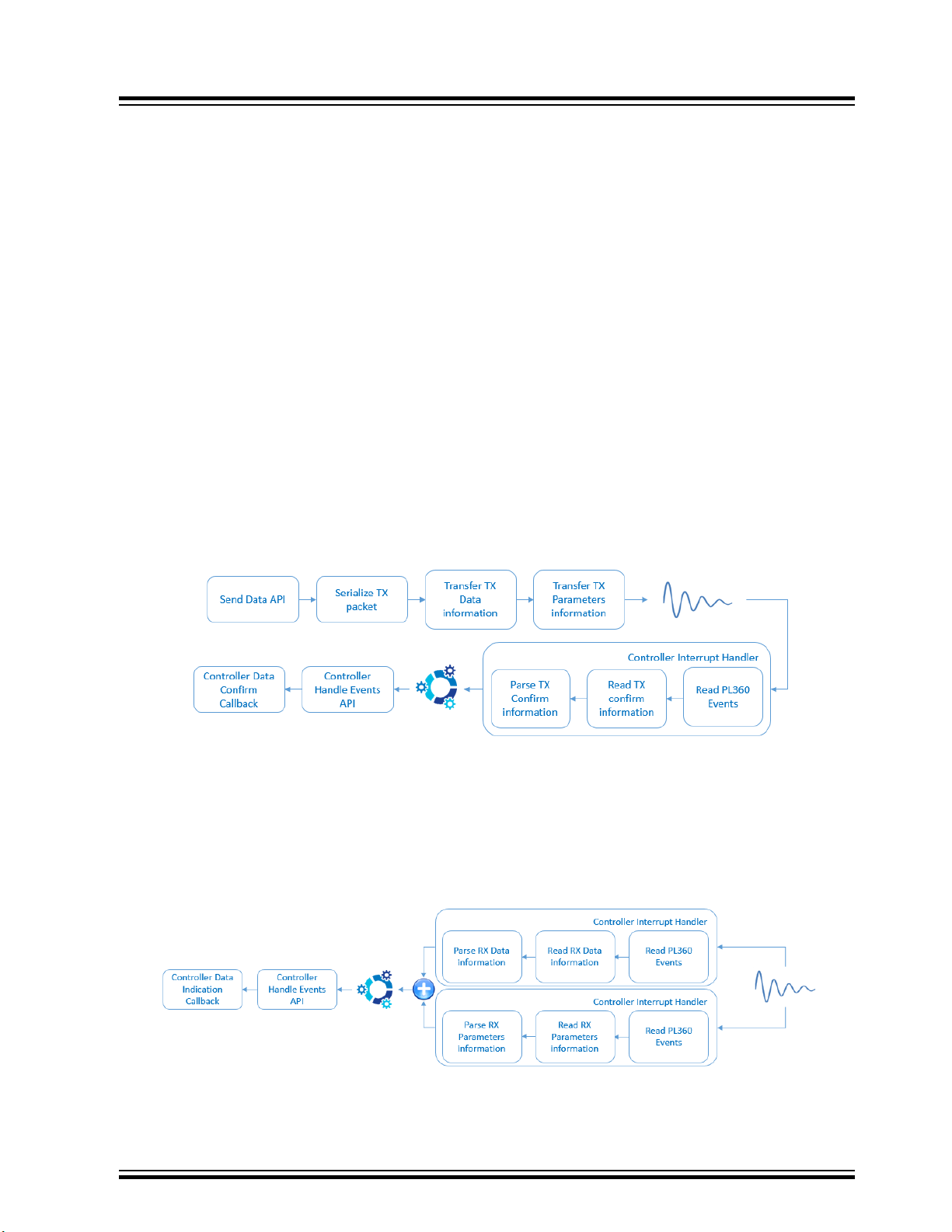
The following figure shows the steps involved in the transmission of a message from the PL360 Host
Controller to the PL360 device.
PL360
Host Interface Management
Figure 6-1. Sequence of Message Transmission
6.2 Message Reception
The following figure shows the steps involved in the reception of a message from the PL360 device to the
PL360 Host Controller.
Figure 6-2. Sequence of Message Reception
© 2018 Microchip Technology Inc.
User Guide
50002738B-page 17
Page 18
7. SPI Protocol
The main interface of the PL360 device is the SPI. The PL360 device employs a protocol to allow the
exchange of formatted data with the PL360 Host Controller. The PL360 SPI protocol uses raw bytes
exchanged on the SPI bus to form high level structures like requests and callbacks.
The PL360 SPI protocol consists of two layers:
• Layer 1: bootloader commands to transfer the firmware and configure the PL360 device
• Layer 2: firmware commands to allow the host MCU application to exchange high level messages
(e.g. PLC data transmission or PLC data reception) with the PL360 embedded firmware
The PL360 SPI Protocol is implemented as a command-response transaction and assumes that one part
is the master (PL360 Host Controller) and the other one is the slave (PL360 embedded firmware).
The format of Command, Response and Data frames is described in the following subsections. The
following points apply:
• There is a response for each command
• Transmitted/received data is divided into packets with variable size
• For a write transaction (slave is receiving data packets), the slave sends a response for each data
packet
• For a read transaction (master is receiving data packets), the master does not send any response
• Boot commands require 8-bit transactions. Firmware commands require 16-bit transactions.
PL360
SPI Protocol
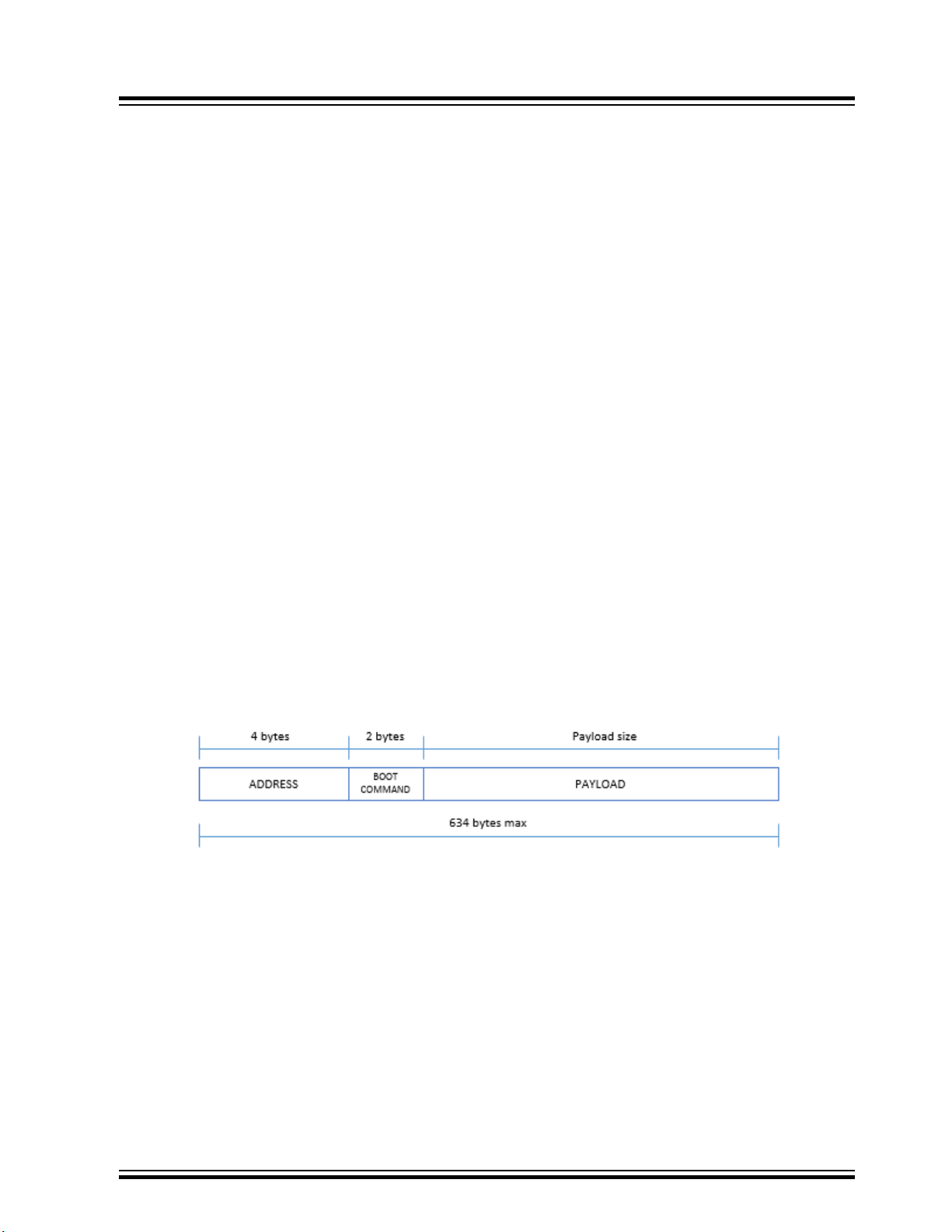
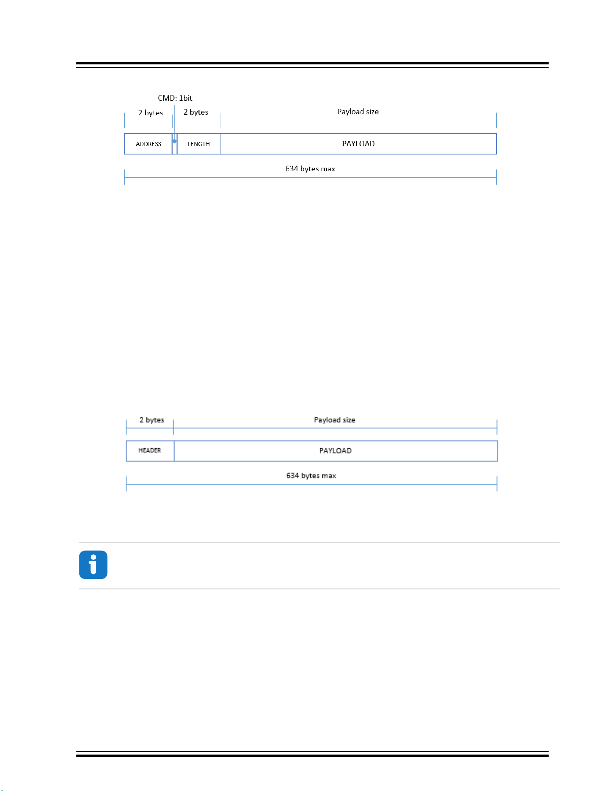
7.1 Boot Command Format
The following frame format is used for boot commands, where the PL360 device supports a DMA address
of four bytes.
Figure 7-1. Boot Command Fields
The address field contains any physical address of the PL360 device.
For further information regarding the boot command and payload fields, please see the PL360 datasheet.
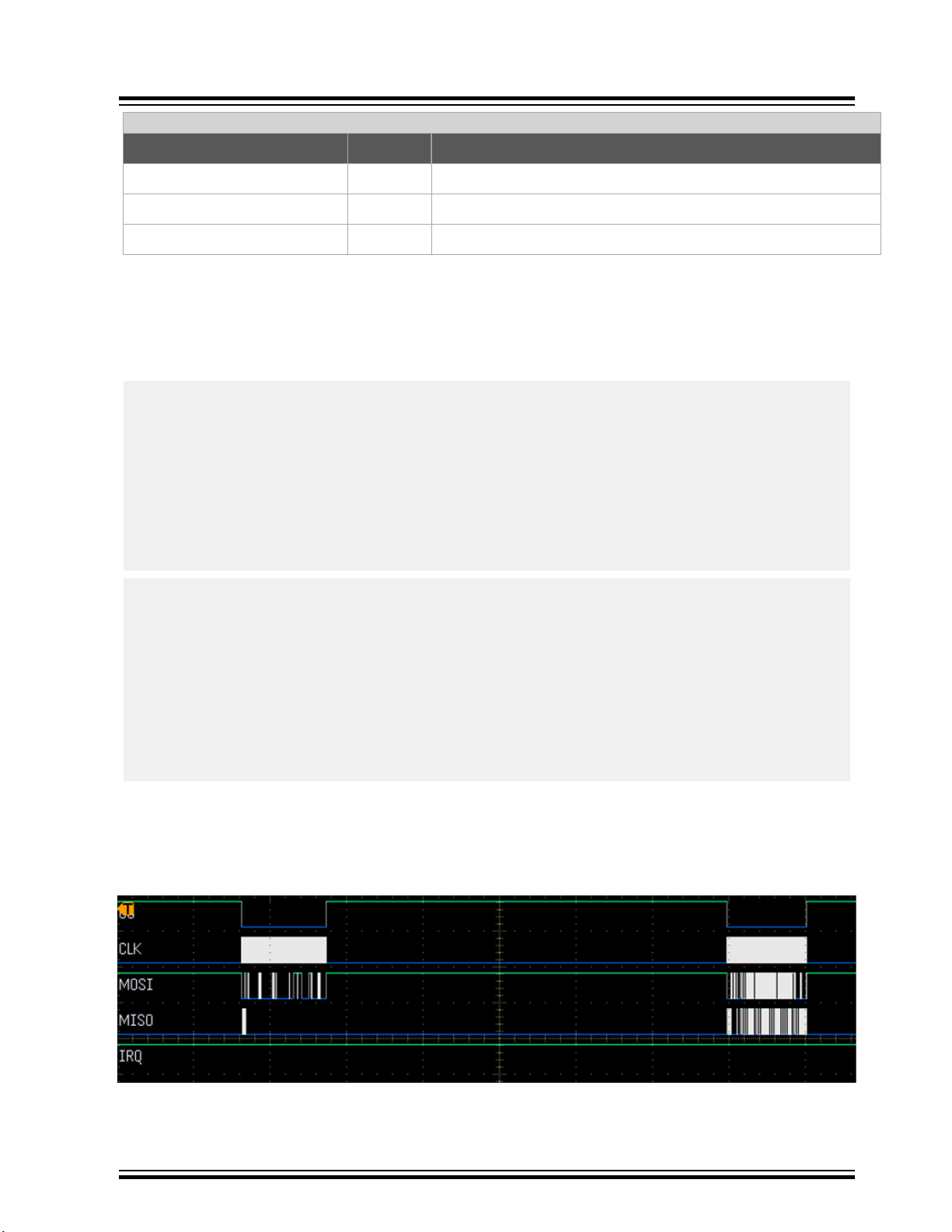
7.2 Boot Response Format
The following frame format is used for boot responses.
© 2018 Microchip Technology Inc.
User Guide
50002738B-page 18
Page 19

PL360
SPI Protocol
The header field is formed by the first 15 bits and it contains the boot signature data
(0b010101100011010). This data is fixed by the PL360 device and it is used to identify the status of the
PL360 device.
The flags field contains information about the reset type of the last reset event:
• USER_RST: User reset
• CM7_RST: Cortex reset
• WDG_RST: Watchdog reset
Table 7-1. Boot Signature Data
31 30 29 28 27 26 25 24
0 1 0 1 0 1 1 0
23 22 21 20 19 18 17 16
0 0 1 1 0 1 0 USER_RST
15 14 13 12 11 10 9 8
CM7_RST WDG_RST – – – – – –
7 6 5 4 3 2 1 0
– – – – – – – –
7.3 Firmware Command Format
The following frame format is used for firmware commands, where the PL360 device supports a DMA
address of two bytes.
© 2018 Microchip Technology Inc.
User Guide
50002738B-page 19
Page 20
PL360
SPI Protocol
Figure 7-2. Firmware Command Fields
The address field contains the identification number of the region to access data. These region numbers are described in section 7.5 Firmware Data Memory Regions.
The CMD field (1 bit), which is the most significant bit of the length field, contains the SPI command:
• Read command: 0
• Write command: 1
The length field (15 bits) contains the number of 16-bit blocks to read.
The payload field depends on the region number to access and on the communication stack in use, G3 or
PRIME. For further information, please refer to atpl360_comm.h file.
7.4 Firmware Response Format
The following frame format is used for firmware responses.
Figure 7-3. Firmware Response Fields
The header field contains the firmware signature data (0x1122). This field is fixed by the PL360
embedded firmware and is used to check if this firmware runs properly.
Info: Due to the 16-bit configuration used in this SPI firmware transaction, the firmware
signature is stored in memory as 0x2211.
The payload field depends on the PLC communication stack in use (G3 or PRIME). For further
information, please refer to atpl360_comm.h file.
7.5 Firmware Data Memory Regions
This section shows the data memory regions defined in the PL360 device depending on which PLC
communication stack is used.
© 2018 Microchip Technology Inc.
User Guide
50002738B-page 20
Page 21

The only difference between PRIME and G3 communication stacks regarding data memory regions is the
CAUTION
number of transmission messages that can be simultaneously queued. In case of G3, only one message
can be queued. In case of PRIME, two transmission messages can be queued simultaneously. This is
possible because there are two transmission buffers defined in the PRIME PL360 embedded firmware,
TX0 and TX1.
In both cases, G3 and PRIME, upper layers are responsible for managing multiple TX times in
order to avoid collisions between them.
7.5.1 G3 Memory Regions
The following table defines memory regions to use with the G3 communication stack:
Table 7-2. G3 Memory Regions Table
Region Name Value Comments
ATPL360_STATUS_INFO_ID 0 Information relative to the system timer and system events
PL360
SPI Protocol
occurrences in the PL360 firmware
ATPL360_TX_PARAM_ID 1 Information relative to parameters of the last transmission
ATPL360_TX_DATA_ID 2 Information relative to data of the last transmission
ATPL360_TX_CFM_ID 3 Information relative to the confirmation of the last transmission
ATPL360_RX_PARAM_ID 4 Information relative to parameters of the last received message
ATPL360_RX_DATA_ID 5 Information relative to data of the last received message
ATPL360_REG_INFO_ID 6 Information relative to internal registers or PIB’s
7.5.2 PRIME Memory Regions
The following table defines memory regions to use with the PRIME communication stack:
Table 7-3. PRIME Memory Regions Table
Region Name Value Comments
ATPL360_STATUS_INFO_ID 0 Information relative to the system timer and system events
ATPL360_TX0_PARAM_ID 1 Information relative to parameters of the last transmission
ATPL360_TX0_DATA_ID 2 Information relative to data of the last transmission (buffer 0)
ATPL360_TX0_CFM_ID 3 Information relative to the confirmation of the last transmission
occurrences in the PL360 firmware
(buffer 0)
(buffer 0)
ATPL360_TX1_PARAM_ID 4 Information relative to parameters of the last transmission
(buffer 1)
ATPL360_TX1_DATA_ID 5 Information relative to data of the last transmission (buffer 1)
ATPL360_TX1_CFM_ID 6 Information relative to the confirmation of the last transmission
(buffer 1)
© 2018 Microchip Technology Inc.
User Guide
50002738B-page 21
Page 22
...........continued
Region Name Value Comments
ATPL360_RX_PARAM_ID 7 Information relative to parameters of the last received message
ATPL360_RX_DATA_ID 8 Information relative to data of the last received message
ATPL360_REG_INFO_ID 9 Information relative to internal registers or PIB’s
7.6 Message Flow for Basic Transactions
This section shows the essential message exchanges and timings.
Related constants affecting below parameters:
/* ! FLAG MASKs for set G3 events */
#define ATPL360_TX_CFM_FLAG_MASK 0x0001
#define ATPL360_RX_DATA_IND_FLAG_MASK 0x0002
#define ATPL360_CD_FLAG_MASK 0x0004
#define ATPL360_REG_RSP_MASK 0x0008
#define ATPL360_RX_QPAR_IND_FLAG_MASK 0x0010
/* ! G3 Event Info MASKs */
#define ATPL360_EV_DAT_LEN_MASK 0x0000FFFF
#define ATPL360_EV_REG_LEN_MASK 0xFFFF0000
#define ATPL360_GET_EV_DAT_LEN_INFO(x) ((uint32_t)x & ATPL360_EV_DAT_LEN_MASK)
#define ATPL360_GET_EV_REG_LEN_INFO(x) (((uint32_t)x & ATPL360_EV_REG_LEN_MASK) >> 16)
PL360
SPI Protocol
/* ! FLAG MASKs for set PRIME events */
#define ATPL360_TX0_CFM_FLAG_MASK 0x0001
#define ATPL360_TX1_CFM_FLAG_MASK 0x0002
#define ATPL360_RX_DATA_IND_FLAG_MASK 0x0004
#define ATPL360_CD_FLAG_MASK 0x0008
#define ATPL360_REG_RSP_MASK 0x0010
#define ATPL360_RX_QPAR_IND_FLAG_MASK 0x0020
/* ! PRIME Event Info MASKs */
#define ATPL360_EV_DAT_LEN_MASK 0x0000FFFF
#define ATPL360_EV_REG_LEN_MASK 0xFFFF0000
#define ATPL360_GET_EV_DAT_LEN_INFO(x) ((uint32_t)x & ATPL360_EV_DAT_LEN_MASK)
#define ATPL360_GET_EV_REG_LEN_INFO(x) (((uint32_t)x & ATPL360_EV_REG_LEN_MASK) >> 16)
7.6.1 G3: Send Message
In a message transmission, there are 2 SPI blocks. The first one is relative to the transmission of G3
parameters of the message, the second one is relative to the data part of the same message.
Figure 7-4. G3 Send Message SPI Sequence
© 2018 Microchip Technology Inc.
User Guide
50002738B-page 22
Page 23
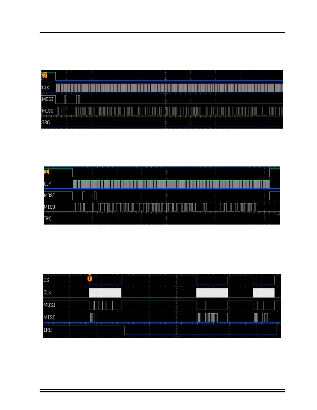
7.6.1.1 G3: Send Parameters
Figure 7-5. G3 Send Parameters SPI Array
In a transmission of parameters, the following can be seen:
• Master (MOSI):
– Send ID memory region(16 bits): 0x0001 (ATPL360_TX_PARAM_ID)
– Send SPI command (1 bit): 1 (write command)
– Send SPI params length (15 bits) (in blocks of 16-bits): 0x14 (40 bytes)
– Send configuration parameters of G3 transmission (40 bytes) [example in CEN-A band]
• Slave (MISO): PL360 device responds with the Firmware Header (0x1122)
• IRQ is not used in this request operation
PL360
SPI Protocol
7.6.1.2 G3: Send Data
Figure 7-6. G3 Send Data SPI Array
In a transmission of data, the following can be seen:
• Master (MOSI):
– Send ID memory region(16 bits): 0x0002 (ATPL360_TX_DATA_ID)
– Send SPI command (1 bit): 1 (write command)
– Send SPI data length (15 bits) (in blocks of 16-bits): 0x04 (8 bytes)
– Send data of G3 transmission (8 bytes)
• Slave (MISO): PL360 device responds with the Firmware Header (0x1122)
• IRQ is not used in this request operation
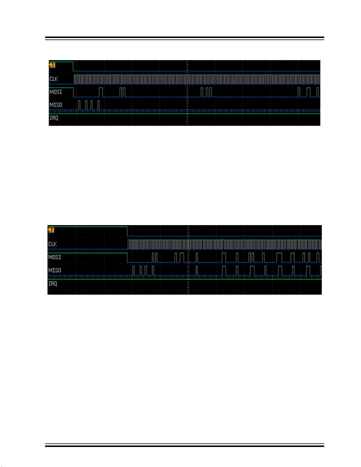
7.6.2 G3: Read TX confirm Information
When message transmission is complete, the PL360 device reports the status of the last transmission.
For that purpose, IRQ is used to notify the PL360 Host Controller that an event has occurred.
© 2018 Microchip Technology Inc.
User Guide
50002738B-page 23
Page 24
PL360
SPI Protocol
Figure 7-7. G3 Read TX Confirm SPI Sequence
In the figure above, the following can be seen:
• IRQ is used to notify of PL360 events
• First SPI transaction corresponds to the retrieval of event information from the PL360 device
• Second SPI transaction corresponds to the retrieval of confirmation data from the PL360 device (if
needed)
7.6.2.1 Get Events Information
Figure 7-8. G3 Get Events Information SPI Array
In the retrieval of event information, the following can be seen:
• Master (MOSI):
– Send ID memory region(16 bits): 0x0000 (ATPL360_STATUS_INFO_ID)
– Send SPI command (1 bit): 0 (read command)
– Send SPI data length (15 bits) (in blocks of 16 bits): 0x04 (8 bytes)
• Slave (MISO):
– Send Firmware Header (16 bits): 0x1122
– Send Firmware Events (16 bits): 0x0001 (ATPL360_TX_CFM_FLAG_MASK)
– Send Firmware Timer reference (32 bits)
– Send Firmware Events Information (32 bits). Only valid in case of data indication
(ATPL360_RX_DATA_IND_FLAG_MASK) or register response (ATPL360_REG_RSP_MASK)
events. It is used to report the length of the data to be read
© 2018 Microchip Technology Inc.
User Guide
50002738B-page 24
Page 25

7.6.2.2 Get Confirmation Data
Figure 7-9. G3 Get Confirmation Data SPI Array
If there is a pending ATPL360_TX_CFM_FLAG_MASK event, it is needed to read information relative to
the TX confirmation event:
• Master (MOSI):
– Send ID memory region(16 bits): 0x0003 (ATPL360_TX_CFM_ID)
– Send SPI command (1 bit): 0 (read command)
– Send SPI data length (15 bits) (in blocks of 16-bits): 0x05 (10 bytes)
• Slave (MISO):
– Send Firmware Header (16 bits): 0x1122
– Send Firmware Events (16 bits): 0x0001 (ATPL360_TX_CFM_FLAG_MASK)
– Send Firmware TX confirmation data:
• RMS calc value (32 bits)
• Transmission Time (32 bits)
• Transmission Result (8 bits)
PL360
SPI Protocol
If there are no pending events to attend, the nterrupt line is disabled.
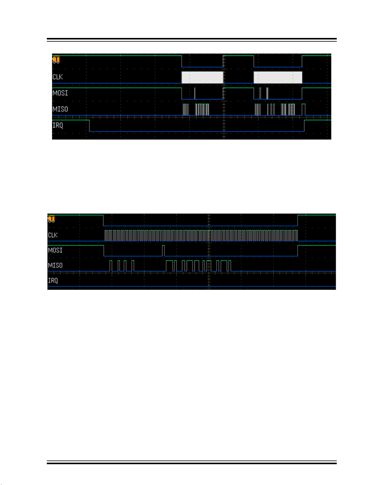
7.6.3 G3: Receive Message
Figure 7-10. G3 Receive Message SPI Sequence
Message reception is composed of four SPI transactions in two interruption blocks:
• IRQ 1: Get data part of the message (two transactions):
– Get Events Information
– Get Data
• IRQ 2: Get parameters part of the message (two transactions):
– Get Events Information
© 2018 Microchip Technology Inc.
User Guide
50002738B-page 25
Page 26

– Get Parameters
7.6.3.1 Get Events Information and Data
Figure 7-11. G3 Get Events Information and Data SPI Arrays
If IRQ occurs (enabled in low), it is first needed to read events reported by the PL360 device.
• Master (MOSI):
– Send ID memory region(16 bits): 0x0000 (ATPL360_STATUS_INFO_ID)
– Send SPI command (1 bit): 0 (read command)
– Send SPI data length (15 bits) (in blocks of 16-bits): 0x04 (8 bytes)
• Slave (MISO):
– Send Firmware Header (16 bits): 0x1122
– Send Firmware Events (16 bits): 0x0002 (ATPL360_RX_DATA_IND_FLAG_MASK)
– Send Firmware Timer reference (32 bits)
– Send Firmware Events Information (32 bits)
• First 16 bits: Not valid
• Second 16 bits: Length of the data to be read in next transaction (D_LEN)
PL360
SPI Protocol
The next transaction gets the data part of the message:
• Master (MOSI):
– Send ID memory region(16 bits): 0x0005 (ATPL360_RX_DATA_ID)
– Send SPI command (1 bit): 0 (read command)
– Send SPI data length (15 bits) (in blocks of 16-bits): Use (D_LEN/2) obtained in previous
transaction
• Slave (MISO):
– Send Firmware Header (16 bits): 0x1122
– Send Firmware Events (16 bits): 0x0002 (ATPL360_RX_DATA_IND_FLAG_MASK)
– Send Firmware RX data (variable)
© 2018 Microchip Technology Inc.
User Guide
50002738B-page 26
Page 27

7.6.3.2 Get Events Information and Parameters
Figure 7-12. G3 Get Events Information and Parameters SPI Arrays
If IRQ occurs (enabled in low), first it is needed to read events reported by the PL360 device.
• Master (MOSI):
– Send ID memory region(16 bits): 0x0000 (ATPL360_STATUS_INFO_ID)
– Send SPI command (1 bit): 0 (read command)
– Send SPI data length (15 bits) (in blocks of 16-bits): 0x04 (8 bytes)
• Slave (MISO):
– Send Firmware Header (16 bits): 0x1122
– Send Firmware Events (16 bits): 0x0010 (ATPL360_RX_QPAR_IND_FLAG_MASK)
– Send Firmware Timer reference (32 bits)
– Send Firmware Events Information (32 bits): Not valid
PL360
SPI Protocol
The next transaction gets the parameters part of the message:
• Master (MOSI):
– Send ID memory region(16 bits): 0x0004 (ATPL360_RX_PARAM_ID)
– Send SPI command (1 bit): 0 (read command)
– Send SPI data length (15 bits) (in blocks of 16-bits): Variable length depending on G3 band
• Slave (MISO):
– Send Firmware Header (16 bits): 0x1122
– Send Firmware Events (16 bits): 0x0010 (ATPL360_RX_QPAR_IND_FLAG_MASK)
– Send Firmware RX parameters. See rx_msg_t structure in atpl360_comm.h file
7.6.4 PRIME: Send Message (Buffer 0)
In a message transmission, there is only one SPI transaction that includes both parameters and data.
Figure 7-13. PRIME Send Message SPI Array
© 2018 Microchip Technology Inc.
User Guide
50002738B-page 27
Page 28

In the figure above, the following can be seen:
• Master (MOSI):
– Send ID memory region(16 bits): 0x0001 (ATPL360_TX0_PARAM_ID)
– Send SPI command (1 bit): 1 (write command)
– Send SPI params length (15 bits) (in blocks of 16-bits): (param length + data length) / 2,
where param length is 12 bytes
– Send configuration parameters of PRIME transmission (12 bytes)
– Send data part of message (variable)
• Slave (MISO): PL360 responds with Firmware Header (0x1122)
IRQ is not used in this request operation.
7.6.5 PRIME: Read TX confirm Information (Buffer 0)
When message transmission is complete, the PL360 device reports the status of the last transmission.
For that purpose, IRQ is used to notify the PL360 Host Controller that an event has occurred.
Figure 7-14. PRIME TX Confirm Information SPI Sequence
PL360
SPI Protocol
In the figure above, the following can be seen:
• IRQ is used to notify of PL360 events
• First SPI transaction corresponds to the retrieval of event information from the PL360 device
• Second SPI transaction corresponds to the retrieval of confirmation data from the PL360 device (if
needed)
7.6.5.1 Get Events Information (Buffer 0)
Figure 7-15. PRIME Events Information SPI Array
© 2018 Microchip Technology Inc.
User Guide
50002738B-page 28
Page 29

It is similar to the flow described in section 7.6.2.1 Get Events Information, but changing the firmware descriptors for the ones applicable to the PRIME PL360 firmware.
7.6.5.2 Get Confirmation Data (Buffer 0)
Figure 7-16. PRIME Confirmation Data SPI Array
It is similar to the flow described in section 7.6.2.2 Get Confirmation Data, but changing the firmware
descriptors for the ones applicable to the PRIME PL360 firmware.
7.6.6 PRIME: Receive Message
Figure 7-17. PRIME Receive Message SPI Sequence
PL360
SPI Protocol
It is similar to the flow described in section 7.6.3 G3: Receive Message, but changing the firmware
descriptors for the ones applicable to the PRIME PL360 firmware.
In this case, two events are read simultaneously, ATPL360_RX_DATA_IND_FLAG_MASK and
ATPL360_RX_QPAR_IND_FLAG_MASK, so there are two consecutive SPI transactions in order to get
data and parameters information from the PL360 device.
7.6.6.1 Get Events Information
Figure 7-18. PRIME Get Events SPI Array
© 2018 Microchip Technology Inc.
User Guide
50002738B-page 29
Page 30
It is similar to the flow described in section 7.6.3.1 Get Events Information and Data, but changing the
firmware descriptors for the ones applicable to the PRIME PL360 firmware.
7.6.6.2 Get Data Information
Figure 7-19. PRIME Get Data SPI Array
It is similar to the flow described in section 7.6.3.1 Get Events Information and Data, but changing the
firmware descriptors for the ones applicable to the PRIME PL360 firmware.
7.6.6.3 Get Parameters Information
Figure 7-20. PRIME Get Parameters SPI Array
PL360
SPI Protocol
It is similar to the flow described in section 7.6.3.2 Get Events Information and Parameters, but changing
the firmware descriptors for the ones applicable to the PRIME PL360 firmware.
7.6.7 Read Register Information
It is possible to get internal information from the PL360 device.
Figure 7-21. Read Register Information SPI Sequence
In the figure above, three SPI transactions can be seen:
• Request register information
• Get events information
© 2018 Microchip Technology Inc.
User Guide
50002738B-page 30
Page 31

• Get register value
7.6.7.1 Request Register Information
Figure 7-22. Request Register Information Array
• Master (MOSI):
– Send ID memory region(16 bits): 0x0006 (ATPL360_REG_INFO_ID) [example with G3]
– Send SPI command (1 bit): 1 (write command)
– Send SPI params length (15 bits) (in blocks of 16-bits): 0x0004 (8 bytes)
– Send register identification (4 bytes). See section 12.2.5 PIB Objects Specification and
Access (G3) or 12.3.4 PIB Objects Specification and Access (PRIME)
– Send length of the register to read (2 bytes)
• Slave (MISO): PL360 device responds with firmware header (0x1122)
PL360
SPI Protocol
7.6.7.2 Get Events Information
Figure 7-23. Get Events Information Array
• Master (MOSI):
– Send ID memory region(16 bits): 0x0000 (ATPL360_STATUS_INFO_ID)
– Send SPI command (1 bit): 0 (read command)
– Send SPI data length (15 bits) (in blocks of 16 bits): 0x04 (8 bytes)
• Slave (MISO):
– Send Firmware Header (16 bits): 0x1122
– Send Firmware Events (16 bits): 0x0008 (ATPL360_REG_RSP_MASK)
– Send Firmware Timer reference (32 bits)
– Send Firmware Events Information (32 bits)
• First 16 bits: Length of the register value to read in next transaction. (D_REG)
• Second 16 bits: Not valid
© 2018 Microchip Technology Inc.
User Guide
50002738B-page 31
Page 32

7.6.7.3 Get Register Value
Figure 7-24. Get Register Value SPI Array
• Master (MOSI):
– Send ID memory region(16 bits): 0x0006 (ATPL360_REG_INFO_ID)
– Send SPI command (1 bit): 0 (read command)
– Send SPI data length (15 bits) (in blocks of 16 bits): Variable length depending on register to
read (D_REG)
• Slave (MISO):
– Send Firmware Header (16 bits): 0x1122
– Send Firmware Events (16 bits): 0x008 (ATPL360_REG_RSP_MASK)
– Send Firmware register value. See section 12.2.5 PIB Objects Specification and Access (G3)
or 12.3.4 PIB Objects Specification and Access (PRIME)
PL360
SPI Protocol
© 2018 Microchip Technology Inc.
User Guide
50002738B-page 32
Page 33

8. Example Applications
CAUTION
Please note that all the provided application examples have been configured to work on
Microchip evaluation boards. When using other hardware, the firmware project must define a
Board Support Package (BSP) customized for that hardware.
Along with the PLC communication stacks, specific application examples are provided in order to show
how to integrate the PL360 Host Controller.
In addition, PHY examples using only the PL360 Host Controller are provided in order to evaluate some
low level parameters and to be used together with a Microchip PLC tool for demonstration purposes.
In case of a G3 stack, applications are provided for CENELEC A, CENELEC B and FCC bands (project
folders with suffixes “_cen_a”, “_cen_b” and “_fcc” in each example). Setting the appropriate band in each
project is made by means of conf_atpl360.h file, as explained in section 5.1 Configure Application.
In case of a PRIME stack, applications are provided for CENELEC A and FCC bands (the same project
folder is used in both bands depending on PRIME configured channel. See 12.3.4.27
ATPL360_REG_CHANNEL_CFG (0x4016)).
PL360
Example Applications
8.1 PHY Examples
8.1.1 PHY Tester
The PHY Tester is an application example that demonstrates the complete performance of the Microchip
PLC PHY layer. This example requires a board and a PC tool. In addition, the Microchip PLC PHY Tester
PC tool (available in the Microchip website) has to be installed on the user’s host PC to interface with the
boards.
The Microchip PLC PHY Tester PC tool configures the devices and performs communication tests.
This example uses the serial interface configured through UART0 at 230400bps.
8.1.2 PHY Sniffer
The PHY Sniffer is an application example to monitor data traffic in the PLC network and then send it via
serial communications to a PC tool and the Microchip PLC Sniffer PC tool (available in the Microchip
website), which has to be installed in the user’s host PC to interface with the board. This example
requires only one board and (obviously) a PLC network to be monitored.
This example uses the serial interface configured through UART0 at 230400bps.
8.1.3 TX Console
Due to PC timing, the Microchip PLC PHY Tester PC tool may present limitations in those applications or
tests that require a very short time interval between consecutive frame transmissions.
The PHY TX Console is an application example that demonstrates the complete performance of the
Microchip PLC PHY Layer avoiding the limitations of timing in the PC host. This way, users can perform
more specific PHY tests (e.g., short time interval between consecutive frames).
This application offers an interface to the user by means of a command console. In this console, users
can configure several transmission parameters such as modulation, frame data length and time interval
between frames. In the console it is also possible to test transmission/reception processes.
© 2018 Microchip Technology Inc.
User Guide
50002738B-page 33
Page 34

Example Applications
This example uses the serial interface configured through UART0 at 921600bps.
PL360
© 2018 Microchip Technology Inc.
User Guide
50002738B-page 34
Page 35

9. Supported Platforms
This chapter describes which hardware platforms are currently supported with the PL360 Host Controller
source code. Usually, a platform usually is comprised of three major components:
• An MCU
• A transceiver chip
• A specific board or even several boards that contain the MCU or the transceiver chip
9.1 Supported MCU Families
Platforms based in SAM4C family MCUs.
The dedicated code for each device of the family can be found in the corresponding subdirectories of the
FW package.
9.2 Supported Transceivers
Currently the supported transceivers are PL360.
PL360
Supported Platforms
9.3 Supported Boards
The boards currently supported are given below:
• PL360MB
9.4 Platform Porting
Platform porting is available only under demand.
© 2018 Microchip Technology Inc.
User Guide
50002738B-page 35
Page 36

10. Abbreviations
AGC Automatic Gain Control
API Application Programming Interface
APP Application
ASF Advanced Software Framework
BER Bit Error Rate
CINR Carrier to Interference + Noise Ratio
DT Delimiter Type
EK Evaluation Kit
EVM Error Vector Magnitude
FCH Frame Control Header
FFT Fast Fourier Transform
PL360
Abbreviations
FW Firmware
GPIO General Purpose Input/Output
HAL Hardware Abstraction Layer
IP Internal Peripheral
IFFT Inverse Fast Fourier Transform
IRQ Interrupt Request
LQI Link Quality Indicator
MCU Microcontroller Unit
MISO Master Input Salve Output
MOSI Master Output Salve Input
PAL Platform Abstraction Layer
PDU Protocol Data Unit
PGA Programmable-Gain Amplifier
PHY Physical Layer
PIB PLC Information Base
PLC Power Line Communication
SPI Serial Peripheral Interface
RD Read
RRC Root Raised Cosine
RS Reed Solomon
RSSI Received Signal Strength Indication
© 2018 Microchip Technology Inc.
User Guide
50002738B-page 36
Page 37

RX Reception
SNR Signal to Noise Ratio
TX Transmission
WR Write
PL360
Abbreviations
© 2018 Microchip Technology Inc.
User Guide
50002738B-page 37
Page 38

11. References
Microchip Smart Energy: http://www.microchip.com/design-centers/smart-energy-products/overview
Microchip Power Line Communications: http://www.microchip.com/design-centers/smart-energy-products/
power-line-communications/overview
Microchip Design Support: http://www.microchip.com/support/hottopics.aspx
G3-PLC Alliance: http://www.g3-plc.com/
PRIME Alliance: http://www.prime-alliance.org/
PL360-EK User Guide, 2018
PL360 Datasheet, 2018
Advanced Software Framework: http://www.microchip.com/avr-support/advanced-software-framework-
(asf)
Atmel Studio: http://www.microchip.com/avr-support/atmel-studio-7
Documents for supported families and boards: http://asf.atmel.com/docs/latest/
PL360
References
© 2018 Microchip Technology Inc.
User Guide
50002738B-page 38
Page 39

Appendix A: PL360 Host Controller API
12. Appendix A: PL360 Host Controller API
This appendix describes all the data structures and functions that are part of the PL360 Host Controller
component.
12.1 Common PHY API
12.1.1 Initialization Function
The PL360 Host Controller must always be initialized when the system starts the execution. The following
function initializes the hardware parameters and configures the controller descriptor:
void atpl360_init(atpl360_descriptor_t *const descr, atpl360_hal_wrapper_t *px_hal_wrapper);
Parameters:
descr Pointer to component descriptor
px_hal_wrapper Pointer to HAL wrapper structure
PL360
This function performs the following actions:
• Sets the handlers for the PLC interruption
• Initializes the PLC SPI service
• And, if necessary, initializes add-on interfaces
The component descriptor offers the customer a set of functions to get access to the PL360 device. It is
defined as a structure of function pointers as follows:
typedef struct atpl360_descriptor {
pf_set_callbacks_t set_callbacks;
pf_send_data_t send_data;
pf_mng_get_cfg_t get_config;
pf_mng_set_cfg_t set_config;
pf_addons_event_t send_addons_cmd;
} atpl360_descriptor_t;
where:
• set_callbacks function is used to set upper layers functions to be executed when a PL360 Host
Controller event has been reported. For further information, please refer to the 12.1.2 Setting
Callbacks chapter.
• send_data function provides a mechanism to send a PLC message through the PL360 device.
For further G3 information, please refer to the G3 12.2.2 PHY-DATA.request chapter. For further
PRIME information, please refer to the PRIME 12.3.1 PHY-DATA.request chapter.
• get_config function provides a read access method to get PL360 internal data. For further
information, please refer to the 12.1.6.2 Get Configuration chapter.
• set_config function provides a write access method to set PL360 internal data. For further
information, please refer to the 12.1.6.1 Set Configuration chapter.
• send_addons_cmd function provides a mechanism to connect PLC Microchip tools to the PL360
device. All information received from these tools should be redirected to this function in order to
pass the information to the PL360 Host Controller
© 2018 Microchip Technology Inc.
User Guide
50002738B-page 39
Page 40

PL360
Appendix A: PL360 Host Controller API
Function pointers are defined as follows:
typedef void (*pf_set_callbacks_t)(atpl360_dev_callbacks_t *dev_cb);
typedef uint8_t (*pf_send_data_t)(tx_msg_t *px_msg);
typedef bool (*pf_mng_get_cfg_t)(uint16_t us_param_id, void *px_value, uint8_t uc_len, bool
b_sync);
typedef bool (*pf_mng_set_cfg_t)(uint16_t us_param_id, void *px_value, uint16_t us_len);
typedef void (*pf_addons_event_t)(uint8_t *px_msg, uint16_t us_len);
The PL360 Host Controller also needs to have access to hardware peripherals. A HAL wrapper structure
is used to separate this hardware and software dependency.
typedef struct atpl360_hal_wrapper {
pf_plc_init_t plc_init;
pf_plc_reset_t plc_reset;
pf_plc_set_handler_t plc_set_handler;
pf_plc_bootloader_cmd_t plc_send_boot_cmd;
pf_plc_write_read_cmd_t plc_write_read_cmd;
pf_plc_enable_int_t plc_enable_int;
pf_plc_delay_t plc_delay;
} atpl360_hal_wrapper_t;
In ASF, Microchip provides a set of example functions to get hardware access. It depends on the
communication stack in use.
• G3: Refer to pplc_if.c/.h files. They are located in
asf.sam.services.plc.pplc_if.atpl360 path
• PRIME. Refer to hal_plc.c/.h files. They are located in asf.thirdparty.prime_ng.hal
path
12.1.2 Setting Callbacks
The user can set their own callbacks using the following function pointer defined in the PL360 Host
Controller descriptor:
typedef void (*pf_set_callbacks_t)(atpl360_dev_callbacks_t *dev_cb);
Parameters:
atpl360_dev_callbacks_t Pointer to callbacks struct
The structure used as input of pf_set_callbacks_t function contains four fields which are the
pointers to the functions to be executed for the different PL360 Host Controller events:
typedef struct atpl360_dev_callbacks {
pf_data_confirm_t data_confirm;
pf_data_indication_t data_indication;
pf_addons_event_t addons_event;
pf_exeption_event_t exception_event;
} atpl360_dev_callbacks_t;
where:
• data_confirm function is used to notify of the result of the last message transmission
• data_indication function is used to notify of the reception of a new message
• addons_event function is used to notify that there is a new message to be sent to a PLC
Microchip Tool
• exception_event function is used to notify of any exception which occurs in the communication
with the PL360 device
© 2018 Microchip Technology Inc.
User Guide
50002738B-page 40
Page 41

Exception values are defined as follow:
typedef enum {
ATPL360_EXCEPTION_UNEXPECTED_SPI_STATUS = 0, /* SPI has detected an unexpected status */
ATPL360_EXCEPTION_SPI_CRITICAL_ERROR, /* SPI critical error. */
ATPL360_EXCEPTION_RESET, /* Reset device */
} atpl360_exception_t;
Tip: SPI critical error means that the PL360 firmware cannot be loaded into the PL360 device.
A possible reason for this would be that the SPI is not working properly.
12.1.3 Enable Function
Once the host descriptor has been initialized and the application callbacks have been set, the PL360
Host Controller must be enabled using the following function:
atpl360_res_t atpl360_enable(uint32_t ul_binary_address, uint32_t ul_binary_len);
Parameters:
PL360
Appendix A: PL360 Host Controller API
ul_binary_address Memory address where the PL360 firmware binary file is located
ul_binary_len Size of the PL360 firmware binary file
This function performs the following actions:
• Disable PLC interrupt
• Transfer firmware binary file to the PL360 device
• Check firmware integrity
• Enable PLC interrupt
12.1.4 Disable Function
The PL360 Host Controller provides a mechanism to disable the notification of PL360 Host Controller
events to the application in order to avoid interrupting the normal flow of the customer application. This
mechanism implies that the PLC activity is stopped in the PL360 device.
void atpl360_disable(void);
12.1.5 Event Handler Function
This function provides a mechanism to notify the PL360 Host Controller events to the customer
application using the previously configured callbacks.
The following function must be called every program cycle or at least once when the host MCU
application receives an interrupt from the PL360 embedded firmware:
void atpl360_handle_events(void);
First, this function checks all PLC events:
• PHY parameters and configuration
• End of transmission of PLC message
• End of reception of PLC message
• Exceptions
© 2018 Microchip Technology Inc.
User Guide
50002738B-page 41
Page 42

And then, it triggers the corresponding PL360 Host Controller callbacks.
12.1.6 Management Primitives
12.1.6.1 Set Configuration
This is done by means of a specific function provided by the controller descriptor:
typedef bool (*pf_mng_set_cfg_t)(uint16_t us_param_id, void *px_value, uint8_t uc_len);
Parameters:
us_param_id PIB ID (see 12.3.4 PIB Objects Specification and Access (PRIME) and
*px_value Pointer to parameter value to set
uc_len Length of parameter
The function returns 0 if the result is invalid, otherwise returns 1.
12.1.6.2 Get Configuration
This is done by means of a specific function provided by the controller descriptor:
PL360
Appendix A: PL360 Host Controller API
12.2.5 PIB Objects Specification and Access (G3))
typedef bool (*pf_mng_get_cfg_t)(uint16_t us_param_id, void *px_value, uint8_t uc_len, bool
b_sync);
Parameters:
us_param_id PIB ID (see 12.3.4 PIB Objects Specification and Access (PRIME) and
*px_value Pointer to parameter value to get
uc_len Length of parameter
b_sync Set synchronous (True) or asynchronous mode (False)
The function returns 0 if the result is invalid, otherwise returns 1.
12.2 G3 PHY API
12.2.1 Bandplan Selection
At compilation time, the G3-PLC bandplan must be defined (i.e.: CENELEC A, CENELEC B, FCC or
ARIB) according to user needs.
In general_defs.h there are four constant options for configuring the bandplan:
/* ! CENELEC A Band Plan (24 - 500 kHz) */
#define ATPL360_WB_CENELEC_A 1
/* ! FCC Band Plan (24 - 500 kHz) */
#define ATPL360_WB_FCC 2
/* ! ARIB Band Plan (24 - 500 kHz) */
#define ATPL360_WB_ARIB 3
/* ! CENELEC-B Band Plan (98 - 122 kHz) */
#define ATPL360_WB_CENELEC_B 4
12.2.5 PIB Objects Specification and Access (G3))
The constant ATPL360_WB has to be set, in file conf_atpl360.h, to the value of one of the constant
options of general_defs.h so that the PHY layer is correctly configured.
© 2018 Microchip Technology Inc.
User Guide
50002738B-page 42
Page 43

12.2.2 PHY-DATA.request
This function sends a frame using the PHY layer. This is done by means of a specific function provided by
the controller descriptor:
typedef uint8_t (*pf_send_data_t)(tx_msg_t *px_msg);
The input parameter structure is the following:
typedef struct tx_msg {
uint8_t *puc_data_buf;
uint32_t ul_tx_time;
uint16_t us_data_len;
uint8_t puc_preemphasis[NUM_SUBBANDS_MAX];
uint8_t puc_tone_map[TONE_MAP_SIZE_MAX];
uint8_t uc_tx_mode;
uint8_t uc_tx_power;
enum mod_types uc_mod_type;
enum mod_schemes uc_mod_scheme;
uint8_t uc_pdc;
uint8_t uc_2_rs_blocks;
enum delimiter_types uc_delimiter_type;
} tx_msg_t;
Fields of the structure:
PL360
Appendix A: PL360 Host Controller API
*puc_data_buf Pointer to data buffer
ul_tx_time Instant when transmission has to start referred to 1μs PHY counter (absolute or
relative value, depending on uc_tx_mode)
us_data_len Length of the data buffer in bytes
puc_preemphasis Preemphasis for transmission. Same as uc_tx_power but for each subband
(Related constants explained below)
puc_tone_map Tone map to use in transmission (Related constants explained below)
uc_tx_mode Transmission mode (forced, delayed, ...) (Related constants explained below)
uc_tx_power Power to transmit [0 = Full gain, 1 = (Full gain - 3dB), 2 = (Full gain - 6dB) and so
on]. Maximum value is 15 (Full gain - 45dBs).
uc_mod_type Modulation type (Related constants explained below)
uc_mod_scheme Modulation scheme (Related constants explained below)
uc_pdc Phase detector counter. Not used; calculated and filled internally by PHY layer
uc_2_rs_blocks Flag to indicate whether 2 RS blocks have to be used (only used in FCC
bandplan)
uc_delimiter_type DT field to be used in header (Related constants explained below)
Related constants affecting above parameters:
/* ! \name TX Mode Bit Mask */
/* ! TX Mode: Forced transmission */
#define TX_MODE_FORCED (1 << 0)
/* ! TX Mode: Absolute transmission */
#define TX_MODE_ABSOLUTE (0 << 1)
/* ! TX Mode: Delayed transmission */
#define TX_MODE_RELATIVE (1 << 1)
/* ! TX Mode: SYNCP Continuous transmission */
#define TX_MODE_SYNCP_CONTINUOUS (1 << 2)
/* ! TX Mode: Symbols Continuous transmission */
© 2018 Microchip Technology Inc.
User Guide
50002738B-page 43
Page 44

Appendix A: PL360 Host Controller API
#define TX_MODE_SYMBOLS_CONTINUOUS (1 << 3)
/* ! TX Mode: Cancel transmission */
#define TX_MODE_CANCEL (1 << 4)
/* Modulation types */
enum mod_types {
MOD_TYPE_BPSK = 0,
MOD_TYPE_QPSK = 1,
MOD_TYPE_8PSK = 2,
MOD_TYPE_QAM = 3,
MOD_TYPE_BPSK_ROBO = 4
};
/* Modulation schemes */
enum mod_schemes {
MOD_SCHEME_DIFFERENTIAL = 0,
MOD_SCHEME_COHERENT = 1
};
/* Frame Delimiter Types */
enum delimiter_types {
DT_SOF_NO_RESP = 0, /* Data frame requiring ACK */
DT_SOF_RESP = 1, /* Data frame Not requiring ACK */
DT_ACK = 2, /* Positive ACK */
DT_NACK = 3 /* Negative ACK */
};
/* ! \name G3 configuration band */
#if ATPL360_WB == ATPL360_WB_CENELEC_A
#define FCH_LEN FCH_LEN_CENELEC_A
#define TONE_MAP_SIZE TONE_MAP_SIZE_CENELEC
#define NUM_SUBBANDS NUM_SUBBANDS_CENELEC_A
#define PROTOCOL_CARRIERS NUM_CARRIERS_CENELEC_A
#define SYNCP_DURATION_US SYNCP_DURATION_CENELEC_A_US
#elif ATPL360_WB == ATPL360_WB_FCC
#define FCH_LEN FCH_LEN_FCC
#define TONE_MAP_SIZE TONE_MAP_SIZE_FCC_ARIB
#define NUM_SUBBANDS NUM_SUBBANDS_FCC
#define PROTOCOL_CARRIERS NUM_CARRIERS_FCC
#define SYNCP_DURATION_US SYNCP_DURATION_FCC_ARIB_US
#elif ATPL360_WB == ATPL360_WB_ARIB
#define FCH_LEN FCH_LEN_ARIB
#define TONE_MAP_SIZE TONE_MAP_SIZE_FCC_ARIB
#define NUM_SUBBANDS NUM_SUBBANDS_ARIB
#define PROTOCOL_CARRIERS NUM_CARRIERS_ARIB
#define SYNCP_DURATION_US SYNCP_DURATION_FCC_ARIB_US
#elif ATPL360_WB == ATPL360_WB_CENELEC_B
#define FCH_LEN FCH_LEN_CENELEC_B
#define TONE_MAP_SIZE TONE_MAP_SIZE_CENELEC
#define NUM_SUBBANDS NUM_SUBBANDS_CENELEC_B
#define PROTOCOL_CARRIERS NUM_CARRIERS_CENELEC_B
#define SYNCP_DURATION_US SYNCP_DURATION_CENELEC_A_US
#endif
#define TONE_MAP_SIZE_MAX TONE_MAP_SIZE_FCC_ARIB
#define NUM_SUBBANDS_MAX NUM_SUBBANDS_FCC
#define PROTOCOL_CARRIERS_MAX NUM_CARRIERS_FCC
PL360
The function returns one of the following transmission result values:
/* TX Result values */
enum tx_result_values {
TX_RESULT_PROCESS = 0, /* Already in process */
TX_RESULT_SUCCESS = 1, /* End successfully */
TX_RESULT_INV_LENGTH = 2, /* Invalid length error */
TX_RESULT_BUSY_CH = 3, /* Busy channel error */
TX_RESULT_BUSY_TX = 4, /* Busy in transmission error */
TX_RESULT_BUSY_RX = 5, /* Busy in reception error */
TX_RESULT_INV_SCHEME = 6, /* Invalid modulation scheme error */
TX_RESULT_TIMEOUT = 7, /* Timeout error */
TX_RESULT_INV_TONEMAP = 8, /* Invalid tone map error */
TX_RESULT_INV_MODE = 9, /* Invalid G3 Mode error */
© 2018 Microchip Technology Inc.
User Guide
50002738B-page 44
Page 45

TX_RESULT_NO_TX = 255, /* No transmission ongoing */
};
12.2.3 PHY-DATA.confirm
This data confirm callback executes the function set by the upper layer at the initialization of the PL360
Host Controller. The pointer to the function is set in:
typedef void (*pf_data_confirm_t)(tx_cfm_t *px_msg_cfm);
The result is reported in the following structure:
typedef struct tx_cfm {
uint32_t ul_rms_calc;
uint32_t ul_tx_time;
enum tx_result_values uc_tx_result;
} tx_cfm_t;
Fields of the structure:
ul_rms_calc RMS_CALC value after transmission. Allows estimation of tx power injected
ul_tx_time Instant when frame transmission ended, referred to 1μs PHY counter
PL360
Appendix A: PL360 Host Controller API
uc_tx_result Tx result (Constants listed in previous section)
The function updates the result value with one of the following values:
/* TX Result values */
enum tx_result_values {
TX_RESULT_PROCESS = 0, /* Already in process */
TX_RESULT_SUCCESS = 1, /* End successfully */
TX_RESULT_INV_LENGTH = 2, /* Invalid length error */
TX_RESULT_BUSY_CH = 3, /* Busy channel error */
TX_RESULT_BUSY_TX = 4, /* Busy in transmission error */
TX_RESULT_BUSY_RX = 5, /* Busy in reception error */
TX_RESULT_INV_SCHEME = 6, /* Invalid modulation scheme error */
TX_RESULT_TIMEOUT = 7, /* Timeout error */
TX_RESULT_INV_TONEMAP = 8, /* Invalid tone map error */
TX_RESULT_INV_MODE = 9, /* Invalid G3 Mode error */
TX_RESULT_NO_TX = 255, /* No transmission ongoing */
};
12.2.4 PHY-DATA.indication
This data indication callback executes the function set by the upper layer at the initialization of the PL360
Host Controller. The pointer to the function is set in:
typedef void (*pf_data_indication_t)(rx_msg_t *px_msg);
The information is reported in the following structure:
typedef struct rx_msg {
uint32_t ul_rx_time;
uint32_t ul_frame_duration;
uint16_t us_rssi;
uint16_t us_data_len;
uint8_t uc_zct_diff;
uint8_t uc_rs_corrected_errors;
enum mod_types uc_mod_type;
enum mod_schemes uc_mod_scheme;
uint32_t ul_mult_agc;
uint16_t us_c_fine;
int16_t ss_offset_meas;
uint8_t uc_agc_active;
uint8_t uc_pga_value;
© 2018 Microchip Technology Inc.
User Guide
50002738B-page 45
Page 46

PL360
Appendix A: PL360 Host Controller API
int16_t ss_snr_fch;
int16_t ss_snr_pay
uint16_t us_payload_corrupted_carriers;
uint16_t us_payload_noised_symbols;
uint8_t uc_payload_snr_worst_carrier;
uint8_t uc_payload_snr_worst_symbol;
uint8_t uc_payload_snr_impulsive;
uint8_t uc_payload_snr_be;
uint8_t uc_payload_snr_background;
uint8_t uc_lqi;
enum delimiter_types uc_delimiter_type;
uint8_t uc_rsrv0;
uint8_t puc_tone_map[TONE_MAP_SIZE_MAX];
uint8_t puc_carrier_snr[PROTOCOL_CARRIERS_MAX];
uint8_t uc_rsrv1;
uint8_t *puc_data_buf;
} rx_msg_t;
Fields of the structure:
ul_rx_time Instant when frame was received (end of frame), referred to 1μs PHY
counter
ul_frame_duration Frame duration in μs (Preamble + FCH + Payload)
us_rssi Reception RSSI in dBuV
us_data_len Length of received frame in bytes
uc_zct_diff Phase difference with transmitting node
uc_rs_corrected_errors Errors corrected by RS
uc_mod_type Modulation type of the last received frame. Related constants defined
in section 12.2.2 PHY-DATA.request
uc_mod_scheme Modulation scheme of the last received frame. Related constants
defined in section 12.2.2 PHY-DATA.request
ul_agc_factor Global amplifying factor of the main branch (21 bits)
us_agc_fine Factor that multiplies the digital input signal (13 bits)
ss_agc_offset_meas DC offset after the ADC that will be removed in case the DC Blocker is
enabled (10 bits)
uc_agc_active Flag to indicate if AGC is active
uc_agc_pga_value Gain value applied to the PGA (3 bits)
ss_snr_fch SNR of the header in quarters of dBs
ss_snr_pay SNR of the payload in quarters of dBs
us_payload_corrupted_carriers Number of corrupted carriers in payload due to narrow/broad-band
noise
us_payload_noised_symbols Number of corrupted symbols in payload due to impulsive noise
uc_payload_snr_worst_carrier SNR for the worst case carrier of the payload in quarters of dBs
uc_payload_snr_worst_symbol SNR for the worst case symbol of the payload in quarters of dBs
uc_payload_snr_impulsive SNR of corrupted symbols in payload due to impulsive noise in
quarters of dBs
© 2018 Microchip Technology Inc.
User Guide
50002738B-page 46
Page 47

PL360
Appendix A: PL360 Host Controller API
uc_payload_snr_band SNR of corrupted carriers in payload due to narrow/broad-band noise
in quarters of dBs
uc_payload_snr_background SNR without taking into account corrupted carriers and symbols in
quarters of dBs
uc_lqi Link Quality Indicator
uc_delimiter_type DT field coming in header. Related constants defined in section 12.2.2
PHY-DATA.request
uc_rsrv0 Reserved for future use
puc_tone_map Tone Map in received frame. Related constants defined in section
12.2.2 PHY-DATA.request
puc_carrier_snr SNR for each carrier in dBs (with offset of 10dB, i.e. value 0 means
-10dB)
uc_ rsrv1 Reserved for future use
puc_data_buf Pointer to data buffer containing received frame
12.2.5 PIB Objects Specification and Access (G3)
The default endianness of all PIBs is little endian, otherwise it is explicitly stated.
12.2.5.1 ATPL360_HOST_DESCRIPTION_ID (0x0100)
PL360 Host Controller description.
Access: Read-only.
Value Range: 10 bytes.
Default Value: “SAM4CMS16C” (for SAM4CMS16_0 core) or “SAM4C16C” (for SAM4C16_0 core).
12.2.5.2 ATPL360_HOST_MODEL_ID (0x010A)
Model identification number of the PL360 Host Controller.
Access: Read-only.
Value Range: 2 bytes.
Default Value: 0x0002.
12.2.5.3 ATPL360_HOST_PHY_ID (0x010C)
Physical identification number of the PL360 Host Controller. It is composed of
ATPL360_HOST_VERSION_ID (0x0112) + ATPL360_HOST_BAND_ID (0x0116).
Access: Read-only.
Value Range: 4 bytes.
Default Value: 0x36010201 for CENELEC A band. 0x36010202 for FCC band. 0x36010203 for ARIB
band. 0x36010204 for CENELEC B band.
12.2.5.4 ATPL360_HOST_PRODUCT_ID (0x0110)
Product identification number of the PL360 Host Controller.
Access: Read-only.
Value Range: 2 bytes.
© 2018 Microchip Technology Inc.
User Guide
50002738B-page 47
Page 48

Default Value: 0x3601.
12.2.5.5 ATPL360_HOST_VERSION_ID (0x0112)
Version number of the PL360 Host Controller.
Access: Read-only.
Value Range: 4 bytes.
Default Value: 0x36010200.
12.2.5.6 ATPL360_HOST_BAND_ID (0x0116)
Workband identification number of the PL360 Host Controller.
Access: Read-only.
Value Range: 1 byte.
Default Value: 1: CENELEC A, 2: FCC, 3: ARIB, 4: CENELEC B.
12.2.5.7 ATPL360_TIME_REF (0x0200)
Time reference in microseconds from the last reset of the PL360 device.
Access: Read-only.
PL360
Appendix A: PL360 Host Controller API
Value Range: 4 bytes.
Default Value: Not applicable.
12.2.5.8 ATPL360_REG_PRODID (0x4000)
Product Identifier of firmware embedded in PL360 device.
Access: Read-only.
Value Range: 8 bytes.
Default Value: “ATPL360”.
12.2.5.9 ATPL360_REG_MODEL (0x4001)
Model Identifier of firmware embedded in PL360 device.
Access: Read-only.
Value Range: 2 bytes.
Default Value: 0x3601.
12.2.5.10 ATPL360_REG_VERSION_STR (0x4002)
Version number of PL360 embedded firmware in string format. The format is "AA.BB.CC.DD", where:
• AA: Corresponds to device model ("36")
• BB: Corresponds to G3 band ["01": CEN A, "02": FCC, "03": ARIB, "04": CEN B]
• CC: Major version number
• DD: Minor version number
Access: Read-only.
Value Range: 11 bytes.
Example Value: “36.01.02.00”.
© 2018 Microchip Technology Inc.
User Guide
50002738B-page 48
Page 49

12.2.5.11 ATPL360_REG_VERSION_NUM (0x4003)
Version number of PL360 embedded firmware in hexadecimal format. The format is 0xAABBCCDD,
where:
• AA: Corresponds to device model (0x36)
• BB: Corresponds to G3 band [0x01: CEN A, 0x02: FCC, 0x03: ARIB, 0x04: CEN B]
• CC: Major version number
• DD: Minor version number
Access: Read-only.
Value Range: 4 bytes.
Example Value: 0x36010200.
12.2.5.12 ATPL360_REG_TONE_MASK (0x4004)
Tone mask for static notching.
Access: Read-write.
Value Range: Depends on the number of carriers which are specified in the G3 band (one byte per
carrier).
PL360
Appendix A: PL360 Host Controller API
Default Value: 0.
12.2.5.13 ATPL360_REG_TONE_MAP_RSP_DATA (0x4005)
Tone Map response data. Best modulation and Tone Map combination to maximize baud-rate and
minimize frame error rate, based on last received message. See 12.2.5.67
ATPL360_REG_TONE_MAP_RSP_ENABLED_MODS (0x403E) to configure enabled modulations for the
selection algorithm.
The format is 0xAABBCCCCCC, where:
• AA: Modulation type
– BPSK: 0x00
– QPSK: 0x01
– 8PSK: 0x02
– ROBO: 0x04
• BB: Modulation scheme
– Differential: 0x00
– Coherent: 0x01
• CCCCCC: Tone Map. 3 bytes (FCC, ARIB bands) or 1 byte (CEN_A, CEN_B bands)
Access: Read-only.
Value Range: 3 bytes (CEN_A, CEN_B bands) or 5 bytes (FCC, ARIB bands).
Default Value: Not applicable.
12.2.5.14 ATPL360_REG_TX_TOTAL (0x4006)
Number of successfully transmitted PDUs.
Access: Read-write.
Value Range: 4 bytes.
Default Value: 0.
© 2018 Microchip Technology Inc.
User Guide
50002738B-page 49
Page 50

12.2.5.15 ATPL360_REG_TX_TOTAL_BYTES (0x4007)
Number of bytes in successfully transmitted PDUs.
Access: Read-write.
Value Range: 4 bytes.
Default Value: 0.
12.2.5.16 ATPL360_REG_TX_TOTAL_ERRORS (0x4008)
Number of unsuccessfully transmitted PDUs.
Access: Read-write.
Value Range: 4 bytes.
Default Value: 0.
12.2.5.17 ATPL360_REG_TX_BAD_BUSY_TX (0x4009)
Number of times when the PL360 device received new data to transmit (send_data) and there is already
data in the TX chain.
Access: Read-write.
Value Range: 4 bytes.
PL360
Appendix A: PL360 Host Controller API
Default Value: 0.
12.2.5.18 ATPL360_REG_TX_BAD_BUSY_CHANNEL (0x400A)
Number of times when the PL360 device received new data to transmit (send_data) and the PLC channel
is busy.
Access: Read-write.
Value Range: 4 bytes.
Default Value: 0.
12.2.5.19 ATPL360_REG_TX_BAD_LEN (0x400B)
Number of times when the PL360 device received new data to transmit (send_data) and the specified
length in transmission parameters is invalid.
Access: Read-write.
Value Range: 4 bytes.
Default Value: 0.
12.2.5.20 ATPL360_REG_TX_BAD_FORMAT (0x400C)
Number of times when the PL360 device received new data to transmit (send_data) and the transmission
parameters are not valid.
Access: Read-write.
Value Range: 4 bytes.
Default Value: 0.
12.2.5.21 ATPL360_REG_TX_TIMEOUT (0x400D)
Number of times when the PL360 device received new data to transmit (send_data) and it cannot
transmit data in the specified time provided by the transmission parameters.
Access: Read-write.
© 2018 Microchip Technology Inc.
User Guide
50002738B-page 50
Page 51

Value Range: 4 bytes.
Default Value: 0.
12.2.5.22 ATPL360_REG_RX_TOTAL (0x400E)
Number of successfully received PDUs.
Access: Read-write.
Value Range: 4 bytes.
Default Value: 0.
12.2.5.23 ATPL360_REG_RX_TOTAL_BYTES (0x400F)
Number of bytes in successfully received PDUs.
Access: Read-write.
Value Range: 4 bytes.
Default Value: 0.
12.2.5.24 ATPL360_REG_RX_RS_ERRORS (0x4010)
Number of corrected errors by RS block in received PDUs.
PL360
Appendix A: PL360 Host Controller API
Access: Read-write.
Value Range: 4 bytes.
Default Value: 0.
12.2.5.25 ATPL360_REG_RX_EXCEPTIONS (0x4011)
Number of time-out errors in received PDUs.
Access: Read-write.
Value Range: 4 bytes.
Default Value: 0.
12.2.5.26 ATPL360_REG_RX_BAD_LEN (0x4012)
Number of errors in FCH length in received PDUs.
Access: Read-write.
Value Range: 4 bytes.
Default Value: 0.
12.2.5.27 ATPL360_REG_RX_BAD_CRC_FCH (0x4013)
Number of errors in FCH CRC in received PDUs.
Access: Read-write.
Value Range: 4 bytes.
Default Value: 0.
12.2.5.28 ATPL360_REG_RX_FALSE_POSITIVE (0x4014)
Number of errors in PDU synchronization phase.
Access: Read-write.
Value Range: 4 bytes.
© 2018 Microchip Technology Inc.
User Guide
50002738B-page 51
Page 52

CAUTION
CAUTION
Appendix A: PL360 Host Controller API
Default Value: 0.
12.2.5.29 ATPL360_REG_RX_BAD_FORMAT (0x4015)
Number of errors in modulation type field included in FCH of received PDUs.
Access: Read-write.
Value Range: 4 bytes.
Default Value: 0.
12.2.5.30 ATPL360_REG_ENABLE_AUTO_NOISE_CAPTURE (0x4016)
Flag to indicate if automatic noise analyzer is enabled in the reception chain. If Automatic mode is
enabled, notch filter parameters (12.2.5.33 ATPL360_REG_RRC_NOTCH_ACTIVE (0x4019), 12.2.5.34
ATPL360_REG_RRC_NOTCH_INDEX (0x401A)) cannot be modified by the user. See 12.2.5.31
ATPL360_REG_TIME_BETWEEN_NOISE_CAPTURES (0x4017), 12.2.5.57
ATPL360_REG_RRC_NOTCH_THR_ON (0x4034), 12.2.5.58 ATPL360_REG_RRC_NOTCH_THR_OFF
(0x4035) to configure parameters related to the Auto-mode.
Access: Read-write.
Value Range: 1 byte [0: Disabled (Manual-mode), 1: Enabled (Auto-mode)].
PL360
Default Value: 1.
12.2.5.31 ATPL360_REG_TIME_BETWEEN_NOISE_CAPTURES (0x4017)
Time in milliseconds between noise captures.
Access: Read-write.
Value Range: 4 bytes.
Default Value: 1000 (1 second).
It is recommended to keep the default value of this parameter. If reduced, the power
consumption could increase. Default value is optimum for power consumption and performance
of noise detection.
12.2.5.32 ATPL360_REG_DELAY_NOISE_CAPTURE_AFTER_RX (0x4018)
Time in microseconds to start a new noise capture after PDU reception/transmission.
Access: Read-write.
Value Range: 4 bytes.
Default Value: 3000 (3 milliseconds).
It is recommended to keep the default value of this parameter. If reduced, there could be
unexpected results.
12.2.5.33 ATPL360_REG_RRC_NOTCH_ACTIVE (0x4019)
Number of notched frequencies with RRC notch filter. For CEN_A, FCC and ARIB bands, up to 5 notched
frequencies are allowed. For CEN_B band, only one notched frequency is allowed.
Access: Depends on 12.2.5.30 ATPL360_REG_ENABLE_AUTO_NOISE_CAPTURE (0x4016) value:
© 2018 Microchip Technology Inc.
User Guide
50002738B-page 52
Page 53

• 1 (Auto-mode): Read-only
• 0 (Manual-mode): Read-write
Value Range: 1 byte. [0: OFF, 1-5: ON].
Default Value: 0.
12.2.5.34 ATPL360_REG_RRC_NOTCH_INDEX (0x401A)
Array of RRC notch filter index values in format unsigned Q7.8. The 7 integer bits indicate the carrier
index (0 –127) for which the notch filter is applied. The 8 decimal bits allow to apply the notch filter to a
frequency which is between two consecutive carriers.
To convert the notch index to frequency (in Hz), the following formula is applied:
F = INDEX * Fs / 65536 , where Fs is the sampling rate in Hz:
• CEN_A, CEN_B bands: Fs = 400000 Hz
• FCC, ARIB bands: Fs = 1200000 Hz
For example:
• CEN_A, INDEX = 8192 (0x2000): F = 8192 * 400000 / 65536 = 50000 Hz
• FCC, INDEX = 20544 (0x5040): F = 20544 * 1200000 / 65536 = 376172 Hz
PL360
Appendix A: PL360 Host Controller API
Access: Depends on 12.2.5.30 ATPL360_REG_ENABLE_AUTO_NOISE_CAPTURE (0x4016) value:
• 1 (Auto-mode): Read-only
• 0 (Manual-mode): Read-write
Value Range: 10 bytes (CEN_A, FCC, ARIB bands) or 2 bytes (CEN_B band). Each group of 2 bytes
corresponds to one notched frequency (Integer part: 0 - 127, Decimal part: 0-255). Number of valid
values depends on 12.2.5.33 ATPL360_REG_RRC_NOTCH_ACTIVE (0x4019).
Default Value: 0.
12.2.5.35 ATPL360_REG_NOISE_PEAK_POWER (0x401B)
Noise peak power. Power of the carrier with more noise power in dBuV. The value is updated only if Automode is enabled (12.2.5.30 ATPL360_REG_ENABLE_AUTO_NOISE_CAPTURE (0x4016)) or noise
capture is triggered through 12.2.5.42 ATPL360_REG_RRC_NOTCH_AUTODETECT (0x4024).
Access: Read-only.
Value Range: 2 bytes.
Default Value: Not applicable.
12.2.5.36 ATPL360_REG_CFG_AUTODETECT_IMPEDANCE (0x401E)
Flag to indicate Autodetect Impedance mode is enabled.
Access: Read-write.
Value Range: 1 byte [0: OFF, 1: ON, 2: only FW AGC enabled]
Default Value: 0.
12.2.5.37 ATPL360_REG_CFG_IMPEDANCE (0x401F)
Impedance setting configured in transmission branch.
Access: Read-write.
Value Range: 1 byte [0: HIGH, 1: LOW, 2: VERY_LOW]
Default Value: 2.
© 2018 Microchip Technology Inc.
User Guide
50002738B-page 53
Page 54

12.2.5.38 ATPL360_REG_ZC_PERIOD (0x4020)
Estimated last Zero Cross period.
Access: Read-only.
Value Range: 4 bytes.
Default Value: Not applicable.
12.2.5.39 ATPL360_REG_FCH_SYMBOLS (0x4021)
Number of symbols in Frame Control Header.
Access: Read-only.
Value Range: 1 byte.
Default Value: Not applicable.
12.2.5.40 ATPL360_REG_PAY_SYMBOLS_TX (0x4022)
Number of payload symbols in last transmitted message.
Access: Read-only.
Value Range: 2 bytes.
PL360
Appendix A: PL360 Host Controller API
Default Value: Not applicable.
12.2.5.41 ATPL360_REG_PAY_SYMBOLS_RX (0x4023)
Number of payload symbols in last received message.
Access: Read-only.
Value Range: 2 bytes.
Default Value: Not applicable.
12.2.5.42 ATPL360_REG_RRC_NOTCH_AUTODETECT (0x4024)
Trigger to start noise analysis. If noise analyzer Manual-mode (12.2.5.30
ATPL360_REG_ENABLE_AUTO_NOISE_CAPTURE (0x4016)) is enabled, noise capture can be
triggered through this PIB by writing 1. Writing 0 has no effect. If noise analyzer auto-mode is enabled,
writing any value has no effect.
Access: Write-only.
Value Range: 1 byte.
Default Value: 0. [0: No effect, 1: Trigger (Manual-mode)].
12.2.5.43 ATPL360_REG_MAX_RMS_TABLE_HI (0x4025)
Values of MAX RMS table in HIGH impedance status. (Refer to section 5.2 Configure Coupling
Parameters).
Access: Read-write.
Value Range: 32 bytes.
Default Value: Provided in atpl360_coup_cfg.h file.
12.2.5.44 ATPL360_REG_MAX_RMS_TABLE_VLO (0x4026)
Values of MAX RMS table in VERY_LOW impedance status. (Refer to section 5.2 Configure Coupling
Parameters).
Access: Read-write.
© 2018 Microchip Technology Inc.
User Guide
50002738B-page 54
Page 55

Value Range: 32 bytes.
Default Value: Provided in atpl360_coup_cfg.h file.
12.2.5.45 ATPL360_REG_THRESHOLDS_TABLE_HI (0x4027)
Values of thresholds table in HIGH impedance status. (Refer to section 5.2 Configure Coupling
Parameters).
Access: Read-write.
Value Range: 64 bytes.
Default Value: Provided in atpl360_coup_cfg.h file.
12.2.5.46 ATPL360_REG_THRESHOLDS_TABLE_LO (0x4028)
Values of thresholds table in LOW impedance status. (Refer to section 5.2 Configure Coupling
Parameters).
Access: Read-write.
Value Range: 64 bytes.
Default Value: Provided in atpl360_coup_cfg.h file.
12.2.5.47 ATPL360_REG_THRESHOLDS_TABLE_VLO (0x4029)
Values of thresholds table in VERY_LOW impedance status. (Refer to section 5.2 Configure Coupling
Parameters).
PL360
Appendix A: PL360 Host Controller API
Access: Read-write.
Value Range: 64 bytes.
Default Value: Provided in atpl360_coup_cfg.h file.
12.2.5.48 ATPL360_REG_PREDIST_COEF_TABLE_HI (0x402A)
Predistorsion coefficients table in HIGH impedance status. (Refer to section 5.2 Configure Coupling
Parameters).
Access: Read-write.
Value Range: 72 bytes (CEN_A), 32 bytes (CEN_B), 144 bytes (FCC) or 108 bytes (ARIB).
Default Value: Provided in atpl360_coup_cfg.h file.
12.2.5.49 ATPL360_REG_PREDIST_COEF_TABLE_LO (0x402B)
Predistorsion coefficients table in LOW impedance status. (Refer to section 5.2 Configure Coupling
Parameters).
Access: Read-write.
Value Range: 72 bytes (CEN_A), 32 bytes (CEN_B), 144 bytes (FCC) or 108 bytes (ARIB).
Default Value: Provided in atpl360_coup_cfg.h file.
12.2.5.50 ATPL360_REG_PREDIST_COEF_TABLE_VLO (0x402C)
Predistorsion coefficients table in VERY_LOW impedance status. (Refer to section 5.2 Configure
Coupling Parameters).
Access: Read-write.
Value Range: 72 bytes (CEN_A), 32 bytes (CEN_B), 144 bytes (FCC) or 108 bytes (ARIB).
Default Value: Provided in atpl360_coup_cfg.h file.
© 2018 Microchip Technology Inc.
User Guide
50002738B-page 55
Page 56

12.2.5.51 ATPL360_REG_GAIN_TABLE_HI (0x402D)
Values of IFFT gains table in HIGH impedance status. (Refer to section 5.2 Configure Coupling
Parameters).
Access: Read-write.
Value Range: 6 bytes.
Default Value: Provided in atpl360_coup_cfg.h file.
12.2.5.52 ATPL360_REG_GAIN_TABLE_LO (0x402E)
Values of IFFT gains table in LOW impedance status. (Refer to section 5.2 Configure Coupling
Parameters).
Access: Read-write.
Value Range: 2 bytes.
Default Value: Provided in atpl360_coup_cfg.h file.
12.2.5.53 ATPL360_REG_GAIN_TABLE_VLO (0x402F)
Values of IFFT gains table in VERY LOW impedance status. (Refer to section 5.2 Configure Coupling
Parameters).
PL360
Appendix A: PL360 Host Controller API
Access: Read-write.
Value Range: 6 bytes.
Default Value: Provided in atpl360_coup_cfg.h file.
12.2.5.54 ATPL360_REG_DACC_TABLE_CFG (0x4030)
Configuration values of DACC peripheral according to hardware configuration. (Refer to section 5.2
Configure Coupling Parameters).
Access: Read-write.
Value Range: 68 bytes.
Default Value: Provided in atpl360_coup_cfg.h file.
12.2.5.55 ATPL360_REG_NUM_TX_LEVELS (0x4032)
Number of transmission levels to use in the PL360 firmware.
Access: Read-write.
Value Range: 1 byte.
Default Value: Provided in atpl360_coup_cfg.h file.
12.2.5.56 ATPL360_REG_CORRECTED_RMS_CALC (0x4033)
RMS value obtained compensated with gain applied by AGC algorithm.
Access: Read-only.
Value Range: 4 bytes.
Default Value: Not applicable.
12.2.5.57 ATPL360_REG_RRC_NOTCH_THR_ON (0x4034)
Activation threshold for narrow band noise (in dBμV quarters, uQ14.2).
Access: Read-write.
© 2018 Microchip Technology Inc.
User Guide
50002738B-page 56
Page 57

Value Range: 2 bytes.
Default Value: 270 (67.5 dBμV).
12.2.5.58 ATPL360_REG_RRC_NOTCH_THR_OFF (0x4035)
Deactivation threshold for narrow band noise (in dBμV quarters, uQ14.2).
Access: Read-write.
Value Range: 2 bytes.
Default Value: 254 (63.5 dBμV).
12.2.5.59 ATPL360_REG_CURRENT_GAIN (0x4036)
Current gain used. It can vary after every transmission if transmission AGC is enabled.
Access: Read-only.
Value Range: 2 bytes.
Default Value: Provided in atpl360_coup_cfg.h file.
12.2.5.60 ATPL360_REG_ZC_CONF_INV (0x4037)
Inverse mode for Zero Crossing Detector.
PL360
Appendix A: PL360 Host Controller API
Access: Read-write.
Value Range: 1 byte [0: Normal mode, 1: Inverted mode]
Default Value: 1.
12.2.5.61 ATPL360_REG_ZC_CONF_FREQ (0x4038)
Initial frequency in Hz for Zero Crossing Detector.
Access: Read-write.
Value Range: 1 byte.
Default Value: 50.
12.2.5.62 ATPL360_REG_ZC_CONF_DELAY (0x4039)
Time Delay in microseconds of external Zero Cross detection circuit.
Access: Read-write.
Value Range: 2 bytes.
Default Value: 176.
12.2.5.63 ATPL360_REG_NOISE_PER_CARRIER (0x403A)
Estimation of noise (in dBµV) in each carrier belonging to the corresponding band. It is measured every
time a noise capture is executed (see 12.2.5.30 ATPL360_REG_ENABLE_AUTO_NOISE_CAPTURE
(0x4016), 12.2.5.31 ATPL360_REG_TIME_BETWEEN_NOISE_CAPTURES (0x4017), 12.2.5.42
ATPL360_REG_RRC_NOTCH_AUTODETECT (0x4024)).
This information is used internally for narrow band noise detection and notch filter activation.
The value is updated only if Auto-mode is enabled (12.2.5.30
ATPL360_REG_ENABLE_AUTO_NOISE_CAPTURE (0x4016)) or noise capture is triggered through
12.2.5.42 ATPL360_REG_RRC_NOTCH_AUTODETECT (0x4024).
Access: Read only.
© 2018 Microchip Technology Inc.
User Guide
50002738B-page 57
Page 58

Value Range: 1 byte per carrier.
CAUTION
CAUTION
Default Value: Not applicable.
12.2.5.64 ATPL360_REG_SYNC_XCORR_THRESHOLD (0x403B)
Correlation threshold for synchronization (preamble detection). The format is uQ0.16. It represents
percentage with respect to the maximum ideal value of correlation (computed internally in PL360).
Access: Read-write.
Value Range: 2 bytes.
Default value: 0x7400 (45.3%).
It is recommended to keep the default value of this parameter in order to maintain expected
reception performance.
12.2.5.65 ATPL360_REG_SYNC_XCORR_PEAK_VALUE (0x403C)
Correlation value in last received PDU. The format is the same described in 12.2.5.64
ATPL360_REG_SYNC_XCORR_THRESHOLD (0x403B).
PL360
Appendix A: PL360 Host Controller API
Access: Read-only.
Value Range: 2 bytes.
Default value: Not applicable.
12.2.5.66 ATPL360_REG_SYNC_SYNCM_THRESHOLD (0x403D)
Threshold for SYNCM detection (once preamble is detected with correlation).
Access: Read-write.
Value Range: 2 bytes.
Default value: 15299.
It is recommended to keep the default value of this parameter in order to maintain expected
reception performance.
12.2.5.67 ATPL360_REG_TONE_MAP_RSP_ENABLED_MODS (0x403E)
Bitmask to enable/disable modulations for modulation and Tone Map selection algorithm (see 12.2.5.13
ATPL360_REG_TONE_MAP_RSP_DATA (0x4005)). Each bit corresponds to a combination of
modulation type and modulation scheme (see Table 12-1).
Table 12-1. ATPL360_REG_TONE_MAP_RSP_ENABLED_MODS Bit-field
Bit 7
Bit 6 Bit 5 Bit 4 Bit 3 Bit 2 Bit 1 Bit 0 (LSB)
(MSB)
8PSK_D 8PSK_C QPSK_D QPSK_C BPSK_D BPSK_C ROBO_D ROBO_C
Access: Read-write.
Value Range: 1 byte (1-255).
Default value: 0xFF (All modulations enabled).
© 2018 Microchip Technology Inc.
User Guide
50002738B-page 58
Page 59

12.2.5.68 ATPL360_REG_PPM_CALIB_ON (0x403F)
Enable the oscillator clock signal to go out by TXRX1 pad. This is useful to measure clock frequency
deviation.
Access: Read-write.
Value Range: 1 byte [0: Disabled, 1: Enabled].
Default value: 0.
12.2.5.69 ATPL360_REG_SFO_ESTIMATION_LAST_RX (0x4040)
Estimation of clock frequency deviation on last received PDU. The estimated deviation is the difference
between transmitter and receiver devices. The format is sQ0.31 (signed). The unit is 0.001 ppm. To
convert to ppm, the read value has to be divided by 1000.
Access: Read-only.
Value Range: 4 bytes.
Default value: Not Applicable.
PL360
Appendix A: PL360 Host Controller API
12.3 PRIME PHY SAP
12.3.1 PHY-DATA.request
This function sends a frame using the PHY layer. This is done by means of a specific function provided by
the controller descriptor:
typedef uint8_t (*pf_send_data_t)(tx_msg_t *px_msg);
The input parameter structure is the following:
typedef struct tx_msg {
uint32_t ul_tx_time;
uint16_t us_data_len;
uint8_t uc_att_level;
enum mod_schemes uc_scheme;
uint8_t uc_disable_rx;
enum mode_types uc_mod_type;
uint8_t uc_tx_mode;
enum buffer_id uc_buffer_id;
uint8_t uc_rsvd;
uint8_t *puc_data_buf;
} tx_msg_t;
Fields of the structure:
ul_tx_time Instant when transmission has to start referred to 1μs PHY counter (absolute
value, not relative). Only used when uc_tx_mode is Delayed transmission
us_data_len Length of the data buffer in bytes
uc_att_level Attenuation level in dBs with which the message must be transmitted
uc_scheme Modulation scheme (Related constants explained below)
uc_disable_rx Disable carrier detect monitor in order to force transmission
uc_mod_type PRIME mode type (Related constants explained below)
uc_tx_mode Transmission mode (Related constants explained below)
© 2018 Microchip Technology Inc.
User Guide
50002738B-page 59
Page 60

Appendix A: PL360 Host Controller API
uc_buffer_id Identificator of the buffer used for transmitting
uc_rsvd Reserved field for future use
*puc_data_buf Pointer to data buffer
Related constants affecting above parameters:
/* ! \name TX Mode Bit Mask */
/* ! TX Mode: Absolute transmission */
#define TX_MODE_ABSOLUTE (0 << 0)
/* ! TX Mode: Delayed transmission */
#define TX_MODE_RELATIVE (1 << 0)
/* ! TX Mode: Cancel transmission */
#define TX_MODE_CANCEL (1 << 1)
/* ! TX Mode: Preamble Continuous transmission */
#define TX_MODE_PREAMBLE_CONTINUOUS (1 << 2)
/* ! TX Mode: Symbols Continuous transmission */
#define TX_MODE_SYMBOLS_CONTINUOUS (1 << 3)
/* ! \name PRIME Mode types */
enum mode_types {
MODE_TYPE_A = 0,
MODE_TYPE_B = 2,
MODE_TYPE_BC = 3,
};
/* ! \name Header types */
enum header_types {
PHY_HT_GENERIC = 0,
PHY_HT_PROMOTION = 1,
PHY_HT_BEACON = 2,
};
/* ! \name PRIME Buffer ID */
enum buffer_id {
TX_BUFFER_0 = 0,
TX_BUFFER_1 = 1,
};
/* ! \name Modulation schemes */
enum mod_schemes {
MOD_SCHEME_DBPSK = 0,
MOD_SCHEME_DQPSK = 1,
MOD_SCHEME_D8PSK = 2,
MOD_SCHEME_DBPSK_C = 4,
MOD_SCHEME_DQPSK_C = 5,
MOD_SCHEME_D8PSK_C = 6,
MOD_SCHEME_R_DBPSK = 12,
MOD_SCHEME_R_DQPSK = 13,
};
PL360
The function returns one of the following transmission result values.
/* TX Result values */
enum tx_result_values {
TX_RESULT_PROCESS = 0, /* Already in process */
TX_RESULT_SUCCESS = 1, /* End successfully */
TX_RESULT_INV_LENGTH = 2, /* Invalid length error */
TX_RESULT_BUSY_CH = 3, /* Busy channel error */
TX_RESULT_BUSY_TX = 4, /* Busy in transmission error */
TX_RESULT_BUSY_RX = 5, /* Busy in reception error */
TX_RESULT_INV_SCHEME = 6, /* Invalid modulation scheme error */
TX_RESULT_TIMEOUT = 7, /* Timeout error */
TX_RESULT_INV_BUFFER = 8, /* Invalid buffer identifier error */
TX_RESULT_INV_MODE = 9, /* Invalid PRIME Mode error */
TX_RESULT_NO_TX = 255, /* No transmission ongoing */
};
© 2018 Microchip Technology Inc.
User Guide
50002738B-page 60
Page 61

12.3.2 PHY-DATA.confirm
This data confirm callback executes the function set by the upper layer at the initialization of the PL360
Host Controller. The pointer to the function is set in:
typedef void (*pf_data_confirm_t)(tx_cfm_t *px_msg_cfm);
The result is reported in the following structure:
typedef struct tx_cfm {
uint32_t ul_tx_time;
uint32_t ul_rms_calc;
enum mode_types uc_mod_type;
enum tx_result_values uc_tx_result;
enum buffer_id uc_buffer_id;
} tx_cfm_t;
Fields of the structure:
ul_tx_time Instant when frame transmission ended, referred to 1μs PHY counter
ul_rms_calc RMS_CALC value after transmission. Allows to estimate Tx power injected
uc_mod_type PRIME mode type (Related constants explained in 12.3.1 PHY-DATA.request)
PL360
Appendix A: PL360 Host Controller API
uc_tx_result Tx result (Constants listed in previous section)
uc_buffer_id Identificator of the buffer used for transmitting
12.3.3 PHY-DATA.indication
This data indication callback executes the function set by the upper layer at the initialization of the PL360
Host Controller. The pointer to the function is set in:
typedef void (*pf_data_indication_t)(rx_msg_t *px_msg);
The information is reported in the following structure:
typedef struct rx_msg {
uint32_t ul_evm_header_acum;
uint32_t ul_evm_payload_acum;
uint32_t ul_rx_time;
uint16_t us_evm_header;
uint16_t us_evm_payload;
uint16_t us_data_len;
enum mod_schemes uc_scheme;
enum mode_types uc_mod_type;
enum header_types uc_header_type;
uint8_t uc_rssi_avg;
uint8_t uc_cinr_avg;
uint8_t uc_cinr_min;
uint8_t uc_ber_soft;
uint8_t uc_ber_soft_max;
uint8_t uc_rsv0;
uint8_t uc_rsv1;
uint8_t *puc_data_buf;
} rx_msg_t;
Fields of the structure:
ul_evm_header_acum Accumulated EVM for header
ul_evm_payload_acum Accumulated EVM for payload
ul_rx_time Reception time in μs
© 2018 Microchip Technology Inc.
User Guide
50002738B-page 61
Page 62

Appendix A: PL360 Host Controller API
us_evm_header EVM for header
us_evm_payload EVM for payload
us_data_len Length of the received data
uc_scheme Modulation scheme of the last received message
uc_mod_type PRIME mode type of the last received message
uc_header_type Header Type of the last received message
uc_rssi_avg Average RSSI
uc_cinr_avg Average CINR
uc_cinr_min Minimum CINR
uc_ber_soft Average Soft BER
uc_ber_soft_max Maximum Soft BER
uc_rsv0 Reserved for future use
uc_rsv1 Reserved for future use
PL360
puc_data_buf Pointer to data buffer containing received frame
12.3.4 PIB Objects Specification and Access (PRIME)
The default endianness of all PIB´s is little endian, otherwise it is explicitly stated.
12.3.4.1 ATPL360_HOST_DESCRIPTION_ID (0x0100)
PL360 Host Controller description.
Access: Read-only.
Value Range: 10 bytes.
Default Value: “SAM4CMS16C” (for SAM4CMS16_0 core) or “SAM4C16C” (for SAM4C16_0 core).
12.3.4.2 ATPL360_HOST_MODEL_ID (0x010A)
Model identification number of the PL360 Host Controller.
Access: Read-only.
Value Range: 2 bytes.
Default Value: 0x0002.
12.3.4.3 ATPL360_HOST_PRODUCT_ID (0x0110)
Product identification number of the PL360 Host Controller.
Access: Read-only.
Value Range: 2 bytes.
Default Value: 0x3600.
12.3.4.4 ATPL360_HOST_VERSION_ID (0x0112)
Version number of the PL360 Host Controller.
Access: Read-only.
Value Range: 4 bytes.
© 2018 Microchip Technology Inc.
User Guide
50002738B-page 62
Page 63

Default Value: 0x36000200.
12.3.4.5 ATPL360_TIME_REF (0x0200)
Time reference in microseconds from the last reset of the PL360 device.
Access: Read-only.
Value Range: 4 bytes.
Default Value: Not applicable.
12.3.4.6 ATPL360_REG_PRODID (0x4000)
Product Identifier of firmware embedded in PL360 device.
Access: Read-only.
Value Range: 8 bytes.
Default Value: “ATPL360”.
12.3.4.7 ATPL360_REG_MODEL (0x4001)
Model Identifier of firmware embedded in PL360 device.
Access: Read-only.
PL360
Appendix A: PL360 Host Controller API
Value Range: 2 bytes.
Default Value: 0x3601.
12.3.4.8 ATPL360_REG_VERSION_STR (0x4002)
Version number of embedded firmware in string format. The format is "AA.BB.CC.DD", where:
• AA: Corresponds to device model ("36")
• BB: Corresponds to PRIME band ["05": One Channel 1 - 8, "07": FCC, "08": ARIB]
• CC: Major version number
• DD: Minor version number
Access: Read-only.
Value Range: 11 bytes.
Example Value: “36.05.02.00”.
12.3.4.9 ATPL360_REG_VERSION_NUM (0x4003)
Version number of embedded firmware in hexadecimal format. The format is 0xAABBCCDD, where:
• AA: Corresponds to device model (0x36)
• BB: Corresponds to PRIME band [0x05: One Channel 1 - 8, 0x07: FCC, 0x08: ARIB]
• CC: Major version number
• DD: Minor version number
Access: Read-only.
Value Range: 4 bytes.
Example Value: 0x36050200.
12.3.4.10 ATPL360_REG_CFG_AUTODETECT_IMPEDANCE (0x4004)
Flag to indicate autodetect impedance mode is enabled.
Access: Read-write.
© 2018 Microchip Technology Inc.
User Guide
50002738B-page 63
Page 64

Value Range: 1 byte [0: OFF, 1: ON, 2: only FW AGC enabled]
Default Value: 0.
12.3.4.11 ATPL360_REG_CFG_IMPEDANCE (0x4005)
Impedance setting configured in transmission branch.
Access: Read-write.
Value Range: 1 byte [0: HIGH, 1: LOW, 2: VERY_LOW]
Default Value: 2.
12.3.4.12 ATPL360_REG_ZC_TIME (0x4006)
Last Zero Cross time in microseconds.
Access: Read-only.
Value Range: 4 bytes.
Default Value: Not applicable.
12.3.4.13 ATPL360_REG_RX_PAY_SYMBOLS (0x4007)
Number of payload symbols in last received message.
PL360
Appendix A: PL360 Host Controller API
Access: Read-only.
Value Range: 2 bytes.
Default Value: Not applicable.
12.3.4.14 ATPL360_REG_TX_PAY_SYMBOLS (0x4008)
Number of payload symbols in last transmitted message.
Access: Read-only.
Value Range: 2 bytes.
Default Value: Not applicable.
12.3.4.15 ATPL360_REG_MAX_RMS_TABLE_HI (0x400A)
Values of MAX RMS table in HIGH impedance status. (Refer to section 5.2 Configure Coupling
Parameters).
Access: Read-write.
Value Range: 32 bytes.
Default Value: Provided in atpl360_coup_cfg.h file.
12.3.4.16 ATPL360_REG_MAX_RMS_TABLE_VLO (0x400B)
Values of MAX RMS table in VERY_LOW impedance status. (Refer to section 5.2 Configure Coupling
Parameters).
Access: Read-write.
Value Range: 32 bytes.
Default Value: Provided in atpl360_coup_cfg.h file.
12.3.4.17 ATPL360_REG_THRESHOLDS_TABLE_HI (0x400C)
Values of thresholds table in HIGH impedance status. (Refer to section 5.2 Configure Coupling
Parameters).
© 2018 Microchip Technology Inc.
User Guide
50002738B-page 64
Page 65

Access: Read-write.
Value Range: 64 bytes.
Default Value: Provided in atpl360_coup_cfg.h file.
12.3.4.18 ATPL360_REG_THRESHOLDS_TABLE_LO (0x400D)
Values of thresholds table in LOW impedance status. (Refer to section 5.2 Configure Coupling
Parameters).
Access: Read-write.
Value Range: 64 bytes.
Default Value: Provided in atpl360_coup_cfg.h file.
12.3.4.19 ATPL360_REG_THRESHOLDS_TABLE_VLO (0x400E)
Values of thresholds table in VERY_LOW impedance status. (Refer to section 5.2 Configure Coupling
Parameters).
Access: Read-write.
Value Range: 64 bytes.
Default Value: Provided in atpl360_coup_cfg.h file.
PL360
Appendix A: PL360 Host Controller API
12.3.4.20 ATPL360_REG_PREDIST_COEF_TABLE_HI (0x400F)
Predistorsion coefficients table in HIGH impedance status. (Refer to section 5.2 Configure Coupling
Parameters).
Access: Read-write.
Value Range: 194 bytes.
Default Value: Provided in atpl360_coup_cfg.h file.
12.3.4.21 ATPL360_REG_PREDIST_COEF_TABLE_LO (0x4010)
Predistorsion coefficients table in LOW impedance status. (Refer to section 5.2 Configure Coupling
Parameters).
Access: Read-write.
Value Range: 194 bytes.
Default Value: Provided in atpl360_coup_cfg.h file.
12.3.4.22 ATPL360_REG_PREDIST_COEF_TABLE_VLO (0x4011)
Predistorsion coefficients table in VERY_LOW impedance status. (Refer to section 5.2 Configure
Coupling Parameters).
Access: Read-write.
Value Range: 194 bytes.
Default Value: Provided in atpl360_coup_cfg.h file.
12.3.4.23 ATPL360_REG_GAIN_TABLE_HI (0x4012)
Values of IFFT gains table in HIGH impedance status. (Refer to section 5.2 Configure Coupling
Parameters).
Access: Read-write.
Value Range: 6 bytes.
© 2018 Microchip Technology Inc.
User Guide
50002738B-page 65
Page 66

Default Value: Provided in atpl360_coup_cfg.h file.
12.3.4.24 ATPL360_REG_GAIN_TABLE_LO (0x4013)
Values of IFFT gains table in LOW impedance status. (Refer to section 5.2 Configure Coupling
Parameters).
Access: Read-write.
Value Range: 6 bytes.
Default Value: Provided in atpl360_coup_cfg.h file.
12.3.4.25 ATPL360_REG_GAIN_TABLE_VLO (0x4014)
Values of IFFT gains table in VERY LOW impedance status. (Refer to section 5.2 Configure Coupling
Parameters).
Access: Read-write.
Value Range: 6 bytes.
Default Value: Provided in atpl360_coup_cfg.h file.
12.3.4.26 ATPL360_REG_DACC_TABLE_CFG (0x4015)
Configuration values of DACC peripheral according to hardware configuration. (Refer to section 5.2
Configure Coupling Parameters).
PL360
Appendix A: PL360 Host Controller API
Access: Read-write.
Value Range: 68 bytes.
Default Value: Provided in atpl360_coup_cfg.h file.
12.3.4.27 ATPL360_REG_CHANNEL_CFG (0x4016)
Number of channel used in transmission and reception in the PL360 device. Channels permitted range
from 1 to 8.
Access: Read-write.
Value Range: 1 byte.
Default Value: 1.
12.3.4.28 ATPL360_REG_NUM_TX_LEVELS (0x4017)
Number of transmission levels to use in the PL360 firmware.
Access: Read-write.
Value Range: 1 bytes.
Default Value: Provided in atpl360_coup_cfg.h file.
12.3.4.29 ATPL360_REG_CORRECTED_RMS_CALC (0x4018)
RMS value obtained before signal adaptation in the TX chain.
Access: Read-only.
Value Range: 4 bytes.
Default Value: Not applicable.
12.3.4.30 ATPL360_REG_CURRENT_GAIN (0x4019)
Current gain used. It can vary after every transmission if transmission AGC is enabled.
© 2018 Microchip Technology Inc.
User Guide
50002738B-page 66
Page 67

Access: Read-only.
Value Range: 2 bytes.
Default Value: Provided in atpl360_coup_cfg.h file.
12.3.4.31 ATPL360_REG_ZC_CONF_INV (0x401A)
Inverse mode for Zero Crossing Detector.
Access: Read-write.
Value Range: 1 byte [0: Normal mode, 1: Inverted mode]
Default Value: 1.
12.3.4.32 ATPL360_REG_ZC_CONF_FREQ (0x401B)
Initial frequency in Hz for Zero Crossing Detector.
Access: Read-write.
Value Range: 1 byte.
Default Value: 50.
12.3.4.33 ATPL360_REG_ZC_CONF_DELAY (0x401C)
Time delay in microseconds of external Zero Cross detection circuit.
PL360
Appendix A: PL360 Host Controller API
Access: Read-write.
Value Range: 2 bytes.
Default Value: 176.
12.3.4.34 ATPL360_REG_SIGNAL_CAPTURE_START (0x401D)
Trigger to start signal capture process.
Access: Write only.
Value range: 9 bytes (see Table 12-2).
Table 12-2. Signal Capture Start Parameters
Byte 0 Byte 1 Byte 2 Byte 3 Byte 4 Byte 5 Byte 6 Byte 7 Byte 8
Mode Start time Duration
where,
• Mode: Set according to the following table:
Table 12-3. Capture Mode Bit-field
bit 7 bit 6 bit 5 bit 4 bit 3 bit 2 bit 1 bit 0
- Time Mode Band Mode Signal
Mode
Channel
– Time Mode: 0: Start time in absolute mode, 1: Start time in relative mode. In any case, time is
always relative to PL360 internal timer reference.
– Band Mode: 0: Channel mode, 1: FCC band mode
© 2018 Microchip Technology Inc.
User Guide
50002738B-page 67
Page 68

– Signal Mode [Only valid if Band Mode = 1]: 0: Low level signals, 1: High level signals. In case
of low level signals, AGC is disabled. In case of high level signals, AGC is fixed to an internal
specific value
– Channel [Only valid if Band Mode = 0]: Select channel to capture from 1 to 8
• Start Time: Start time in microseconds referenced to PL360 internal timer
• Duration: Duration time in microseconds. Maximum duration depends on the selected Band Mode.
In case of channel mode, maximum duration is fixed to 80 seconds. In case of FCC band mode,
maximum duration is fixed to 30 seconds
12.3.4.35 ATPL360_REG_SIGNAL_CAPTURE_STATUS (0x401E)
Get the status of signal capture process.
Access: Read only.
Value range: 2 bytes (see Table 12-4).
Table 12-4. Signal Capture Status Parameters
Byte 0 Byte 1
Num_frags Capture State
PL360
Appendix A: PL360 Host Controller API
where,
• Num_frags: Number of fragments of 255 bytes to complete all capture data.
• Capture State: The status of the last capture process. [0: Capture Idle, 1: Capture Running, 2:
Capture Ready]
12.3.4.36 ATPL360_REG_SIGNAL_CAPTURE_FRAGMENT (0x401F)
Number of fragment of signal to extract. It must be set before the capture is done.
Access: Read-write.
Value Range: 1 byte.
Default Value: 0.
12.3.4.37 ATPL360_REG_SIGNAL_CAPTURE_DATA (0x4020)
Signal capture data buffer.
Access: Read only.
Value Range: 255 bytes.
Default Value: Not applicable.
12.3.4.38 ATPL360_REG_ENABLE_AUTO_NOISE_CAPTURE (0x4021)
Flag to indicate if automatic noise analyzer is enabled in the reception chain. If Automatic mode is
enabled, notch filter parameters (12.2.5.33 ATPL360_REG_RRC_NOTCH_ACTIVE (0x4019), 12.3.4.42
ATPL360_REG_RRC_NOTCH_INDEX (0x4025)) cannot be modified by the user. See 12.3.4.39
ATPL360_REG_TIME_BETWEEN_NOISE_CAPTURES (0x4022), 12.3.4.45
ATPL360_REG_RRC_NOTCH_THR_ON (0x4028), 12.3.4.46 ATPL360_REG_RRC_NOTCH_THR_OFF
(0x4029) to configure parameters related to the Auto-mode.
Access: Read-write.
Value Range: 1 byte [0: Disabled (Manual-mode), 1: Enabled (Auto-mode)].
Default Value: 1.
© 2018 Microchip Technology Inc.
User Guide
50002738B-page 68
Page 69

CAUTION
CAUTION
Appendix A: PL360 Host Controller API
12.3.4.39 ATPL360_REG_TIME_BETWEEN_NOISE_CAPTURES (0x4022)
Time in milliseconds between noise captures.
Access: Read-write.
Value Range: 4 bytes.
Default Value: 1000 (1 second).
It is recommended to keep the default value of this parameter. If reduced, the power
consumption could increase. Default value is optimum for power consumption and performance
of noise detection.
12.3.4.40 ATPL360_REG_DELAY_NOISE_CAPTURE_AFTER_RX (0x4023)
Time in microseconds to start a new noise capture after PDU reception/transmission.
Access: Read-write.
Value Range: 4 bytes.
Default Value: 3000 (3 milliseconds).
PL360
It is recommended to keep the default value of this parameter. If reduced, there could be
unexpected results.
12.3.4.41 ATPL360_REG_RRC_NOTCH_ACTIVE (0x4024)
Flag to indicate if RRC notch filter is active.
Access: Depends on 12.2.5.30 ATPL360_REG_ENABLE_AUTO_NOISE_CAPTURE (0x4016) value:
• 1 (Auto-mode): Read-only
• 0 (Manual-mode): Read-write
Value Range: 1 byte. [0: OFF, 1: ON].
Default Value: 0.
12.3.4.42 ATPL360_REG_RRC_NOTCH_INDEX (0x4025)
RRC notch filter index value in format unsigned Q9.7. The 9 integer bits indicate the carrier index for
which the notch filter is applied. The 7 decimal bits allow to apply the notch filter to a frequency which is
between two consecutive carriers. The index is mapped to the corresponding carrier considering baseband.
To convert the notch index to frequency (in Hz), the following formula is applied:
F = F’ + 65429.6875 + (Ch - 1) * 54687.5 , where Ch is the PRIME channel used (1-8, see 12.3.4.27
ATPL360_REG_CHANNEL_CFG (0x4016)) and F':
• If INDEX < 32768 : F' = INDEX * k
• If INDEX ≥ 32768 : F' = (INDEX-65536) * k
where k = 1000000 / (2048 * 128) = 3.814697265625 Hz
For example:
• Channel 1, INDEX = 64768 (0xFD00): F = (64768 - 65536) * k + 65429.6875 = 62500 Hz
© 2018 Microchip Technology Inc.
User Guide
50002738B-page 69
Page 70

• Channel 4, INDEX = 16 (0x0010): F = 16 * k + 65429.6875 + 3 * 54687.5 = 229553 Hz
Access: Depends on 12.2.5.30 ATPL360_REG_ENABLE_AUTO_NOISE_CAPTURE (0x4016) value:
• 1 (Auto-mode): Read-only
• 0 (Manual-mode): Read-write
Value Range: 2 bytes (Integer part: 0 - 511, Decimal part: 0-127).
Default Value: 0.
12.3.4.43 ATPL360_REG_NOISE_PEAK_POWER (0x4026)
Noise peak power. Power of the carrier with more noise power in dBuV. The value is updated only if Automode is enabled (12.3.4.38 ATPL360_REG_ENABLE_AUTO_NOISE_CAPTURE (0x4021)) or noise
capture is triggered through 12.3.4.44 ATPL360_REG_RRC_NOTCH_AUTODETECT (0x4027).
Access: Read-only.
Value Range: 2 bytes.
Default Value: Not applicable.
12.3.4.44 ATPL360_REG_RRC_NOTCH_AUTODETECT (0x4027)
Trigger to start noise analysis. If noise analyzer Manual-mode (12.3.4.38
ATPL360_REG_ENABLE_AUTO_NOISE_CAPTURE (0x4021)) is enabled, noise capture can be
triggered through this PIB by writing 1. Writing 0 has no effect. If noise analyzer Auto-mode is enabled,
writing any value has no effect.
PL360
Appendix A: PL360 Host Controller API
Access: Write-only.
Value Range: 1 byte.
Default Value: 0. [0: No effect, 1: Trigger].
12.3.4.45 ATPL360_REG_RRC_NOTCH_THR_ON (0x4028)
Activation threshold for narrow band noise (in dBμV quarters, uQ14.2).
Access: Read-write.
Value Range: 2 bytes.
Default Value: 272 (68 dBμV).
12.3.4.46 ATPL360_REG_RRC_NOTCH_THR_OFF (0x4029)
Deactivation threshold for narrow band noise (in dBμV quarters, uQ14.2).
Access: Read-write.
Value Range: 2 bytes.
Default Value: 264 (66 dBμV).
12.3.4.47 ATPL360_REG_TX_TOTAL (0x402A)
Number of successfully transmitted PDUs.
Access: Read-write.
Value Range: 4 bytes.
Default Value: 0.
12.3.4.48 ATPL360_REG_TX_TOTAL_BYTES (0x402B)
Number of bytes in successfully transmitted PDUs.
© 2018 Microchip Technology Inc.
User Guide
50002738B-page 70
Page 71

Access: Read-write.
Value Range: 4 bytes.
Default Value: 0.
12.3.4.49 ATPL360_REG_TX_TOTAL_ERRORS (0x402C)
Number of unsuccessfully transmitted PDUs.
Access: Read-write.
Value Range: 4 bytes.
Default Value: 0.
12.3.4.50 ATPL360_REG_TX_BAD_BUSY_TX (0x402D)
Number of times when the PL360 device received new data to transmit (send_data) and there is already
data in the TX chain.
Access: Read-write.
Value Range: 4 bytes.
Default Value: 0.
PL360
Appendix A: PL360 Host Controller API
12.3.4.51 ATPL360_REG_TX_BAD_BUSY_CHANNEL (0x402E)
Number of times when the PL360 device received new data to transmit (send_data) and the PLC channel
is busy.
Access: Read-write.
Value Range: 4 bytes.
Default Value: 0.
12.3.4.52 ATPL360_REG_TX_BAD_LEN (0x402F)
Number of times when the PL360 device received new data to transmit (send_data) and the specified
length in transmission parameters is invalid.
Access: Read-write.
Value Range: 4 bytes.
Default Value: 0.
12.3.4.53 ATPL360_REG_TX_BAD_FORMAT (0x4030)
Number of times when the PL360 device received new data to transmit (send_data) and the transmission
parameters are not valid.
Access: Read-write.
Value Range: 4 bytes.
Default Value: 0.
12.3.4.54 ATPL360_REG_TX_TIMEOUT (0x4031)
Number of times when the PL360 device received new data to transmit (send_data) and it cannot
transmit data in the specified time provided by the transmission parameters.
Access: Read-write.
Value Range: 4 bytes.
© 2018 Microchip Technology Inc.
User Guide
50002738B-page 71
Page 72

Default Value: 0.
12.3.4.55 ATPL360_REG_RX_TOTAL (0x4032)
Number of successfully received PDUs.
Access: Read-write.
Value Range: 4 bytes.
Default Value: 0.
12.3.4.56 ATPL360_REG_RX_TOTAL_BYTES (0x4033)
Number of bytes in successfully received PDUs.
Access: Read-write.
Value Range: 4 bytes.
Default Value: 0.
12.3.4.57 ATPL360_REG_RX_EXCEPTIONS (0x4034)
Number of time-out errors in received PDUs.
Access: Read-write.
PL360
Appendix A: PL360 Host Controller API
Value Range: 4 bytes.
Default Value: 0.
12.3.4.58 ATPL360_REG_RX_BAD_LEN (0x4035)
Number of errors in FCH length in received PDUs.
Access: Read-write.
Value Range: 4 bytes.
Default Value: 0.
12.3.4.59 ATPL360_REG_RX_BAD_CRC_FCH (0x4036)
Number of errors in FCH CRC in received PDUs.
Access: Read-write.
Value Range: 4 bytes.
Default Value: 0.
12.3.4.60 ATPL360_REG_RX_FALSE_POSITIVE (0x4037)
Number of errors in PDU synchronization phase.
Access: Read-write.
Value Range: 4 bytes.
Default Value: 0.
12.3.4.61 ATPL360_REG_RX_BAD_FORMAT (0x4038)
Number of errors in modulation type field included in FCH of received PDUs.
Access: Read-write.
Value Range: 4 bytes.
Default Value: 0.
© 2018 Microchip Technology Inc.
User Guide
50002738B-page 72
Page 73

12.3.4.62 ATPL360_REG_NOISE_PER_CARRIER (0x4039)
Estimation of noise (in dBµV) in each carrier belonging to the corresponding band. It is measured every
time a noise capture is executed (see 12.3.4.38 ATPL360_REG_ENABLE_AUTO_NOISE_CAPTURE
(0x4021), 12.3.4.39 ATPL360_REG_TIME_BETWEEN_NOISE_CAPTURES (0x4022), 12.3.4.44
ATPL360_REG_RRC_NOTCH_AUTODETECT (0x4027)).
This information is used internally for narrow band noise detection and notch filter activation.
The value is updated only if Auto-mode is enabled (12.3.4.38
ATPL360_REG_ENABLE_AUTO_NOISE_CAPTURE (0x4021)) or noise capture is triggered through
12.3.4.44 ATPL360_REG_RRC_NOTCH_AUTODETECT (0x4027).
Access: Read only.
Value Range: 1 byte per carrier.
Default Value: Not applicable.
12.3.4.63 ATPL360_REG_PPM_CALIB_ON (0x403A)
Enable the oscillator clock signal to go out by TXRX1 pad. This is useful to measure clock frequency
deviation.
Access: Read-write.
PL360
Appendix A: PL360 Host Controller API
Value Range: 1 byte [0: Disabled, 1: Enabled].
Default value: 0.
© 2018 Microchip Technology Inc.
User Guide
50002738B-page 73
Page 74

13. Appendix B: ZC Offset Configuration
The PHY layer calculates the electrical phase difference between transmitter and receiver for a given
frame. To do so, both devices have to be able to read the Zero Cross time of the mains.
The PL360 device has a dedicated input pin to be connected to a signal which provides such mains zero
cross.
Due to design reasons, the signal entering the PL360 device may not be fully synchronized with the real
mains zero cross. To handle this, a PIB is available (ATPL360_REG_ZC_CONF_DELAY) to set the delay,
in µs, between mains zero cross and the signal provided to the PL360 device. The delay has to be
measured between the highest point of the mains signal and the middle of the positive pulse provided to
the PL360 device (see Figure 13-1). Default value of this parameter is 176 µs.
Other PIBs for Zero Cross are:
• ATPL360_REG_ZC_CONF_INV: It indicates if the pulse is positive (value 0), as in Figure 13-1, or
negative (value 1). The default value is 1
• ATPL360_REG_ZC_CONF_FREQ: It is the expected frequency of the mains signal, in Hz. The
system is able to adapt itself to a different frequency of the mains signal, but the closer the
configured parameter is to the actual frequency, the faster the adaptation will be. The default value
is 50 Hz
PL360
Appendix B: ZC Offset Configuration
Figure 13-1. ZC_Delay calculation
© 2018 Microchip Technology Inc.
User Guide
50002738B-page 74
Page 75

14. Revision History
14.1 Rev A – 03/2018
Document Initial document release.
14.2 Rev B - 10/2018
12.2.5 PIB Objects Specification and Access (G3) Updated sections 12.2.5.13 , 12.2.5.30 ,
PL360
Revision History
12.2.5.31 , 12.2.5.32 , 12.2.5.33 , 12.2.5.34 ,
12.2.5.35 , 12.2.5.42 , 12.2.5.57 , 12.2.5.58 ,
12.2.5.63 .
Added sections 12.2.5.64 , 12.2.5.65 , 12.2.5.66 ,
12.2.5.67 , 12.2.5.68 , 12.2.5.69 .
12.3.4 PIB Objects Specification and Access
(PRIME)
Updated sections 12.3.4.38 , 12.3.4.39 ,
12.3.4.40 , 12.3.4.41 , 12.3.4.42 , 12.3.4.43 ,
12.3.4.44 , 12.3.4.45 , 12.3.4.46 , 12.3.4.62 .
Added section 12.3.4.63 .
© 2018 Microchip Technology Inc.
User Guide
50002738B-page 75
Page 76

PL360
The Microchip Web Site
Microchip provides online support via our web site at http://www.microchip.com/. This web site is used as
a means to make files and information easily available to customers. Accessible by using your favorite
Internet browser, the web site contains the following information:
• Product Support – Data sheets and errata, application notes and sample programs, design
resources, user’s guides and hardware support documents, latest software releases and archived
software
• General Technical Support – Frequently Asked Questions (FAQ), technical support requests,
online discussion groups, Microchip consultant program member listing
• Business of Microchip – Product selector and ordering guides, latest Microchip press releases,
listing of seminars and events, listings of Microchip sales offices, distributors and factory
representatives
Customer Change Notification Service
Microchip’s customer notification service helps keep customers current on Microchip products.
Subscribers will receive e-mail notification whenever there are changes, updates, revisions or errata
related to a specified product family or development tool of interest.
To register, access the Microchip web site at http://www.microchip.com/. Under “Support”, click on
“Customer Change Notification” and follow the registration instructions.
Customer Support
Users of Microchip products can receive assistance through several channels:
• Distributor or Representative
• Local Sales Office
• Field Application Engineer (FAE)
• Technical Support
Customers should contact their distributor, representative or Field Application Engineer (FAE) for support.
Local sales offices are also available to help customers. A listing of sales offices and locations is included
in the back of this document.
Technical support is available through the web site at: http://www.microchip.com/support
Microchip Devices Code Protection Feature
Note the following details of the code protection feature on Microchip devices:
• Microchip products meet the specification contained in their particular Microchip Data Sheet.
• Microchip believes that its family of products is one of the most secure families of its kind on the
market today, when used in the intended manner and under normal conditions.
• There are dishonest and possibly illegal methods used to breach the code protection feature. All of
these methods, to our knowledge, require using the Microchip products in a manner outside the
operating specifications contained in Microchip’s Data Sheets. Most likely, the person doing so is
engaged in theft of intellectual property.
• Microchip is willing to work with the customer who is concerned about the integrity of their code.
© 2018 Microchip Technology Inc.
User Guide
50002738B-page 76
Page 77

PL360
• Neither Microchip nor any other semiconductor manufacturer can guarantee the security of their
code. Code protection does not mean that we are guaranteeing the product as “unbreakable.”
Code protection is constantly evolving. We at Microchip are committed to continuously improving the
code protection features of our products. Attempts to break Microchip’s code protection feature may be a
violation of the Digital Millennium Copyright Act. If such acts allow unauthorized access to your software
or other copyrighted work, you may have a right to sue for relief under that Act.
Legal Notice
Information contained in this publication regarding device applications and the like is provided only for
your convenience and may be superseded by updates. It is your responsibility to ensure that your
application meets with your specifications. MICROCHIP MAKES NO REPRESENTATIONS OR
WARRANTIES OF ANY KIND WHETHER EXPRESS OR IMPLIED, WRITTEN OR ORAL, STATUTORY
OR OTHERWISE, RELATED TO THE INFORMATION, INCLUDING BUT NOT LIMITED TO ITS
CONDITION, QUALITY, PERFORMANCE, MERCHANTABILITY OR FITNESS FOR PURPOSE.
Microchip disclaims all liability arising from this information and its use. Use of Microchip devices in life
support and/or safety applications is entirely at the buyer’s risk, and the buyer agrees to defend,
indemnify and hold harmless Microchip from any and all damages, claims, suits, or expenses resulting
from such use. No licenses are conveyed, implicitly or otherwise, under any Microchip intellectual
property rights unless otherwise stated.
Trademarks
The Microchip name and logo, the Microchip logo, AnyRate, AVR, AVR logo, AVR Freaks, BitCloud,
chipKIT, chipKIT logo, CryptoMemory, CryptoRF, dsPIC, FlashFlex, flexPWR, Heldo, JukeBlox, KeeLoq,
Kleer, LANCheck, LINK MD, maXStylus, maXTouch, MediaLB, megaAVR, MOST, MOST logo, MPLAB,
OptoLyzer, PIC, picoPower, PICSTART, PIC32 logo, Prochip Designer, QTouch, SAM-BA, SpyNIC, SST,
SST Logo, SuperFlash, tinyAVR, UNI/O, and XMEGA are registered trademarks of Microchip Technology
Incorporated in the U.S.A. and other countries.
ClockWorks, The Embedded Control Solutions Company, EtherSynch, Hyper Speed Control, HyperLight
Load, IntelliMOS, mTouch, Precision Edge, and Quiet-Wire are registered trademarks of Microchip
Technology Incorporated in the U.S.A.
Adjacent Key Suppression, AKS, Analog-for-the-Digital Age, Any Capacitor, AnyIn, AnyOut, BodyCom,
CodeGuard, CryptoAuthentication, CryptoAutomotive, CryptoCompanion, CryptoController, dsPICDEM,
dsPICDEM.net, Dynamic Average Matching, DAM, ECAN, EtherGREEN, In-Circuit Serial Programming,
ICSP, INICnet, Inter-Chip Connectivity, JitterBlocker, KleerNet, KleerNet logo, memBrain, Mindi, MiWi,
motorBench, MPASM, MPF, MPLAB Certified logo, MPLIB, MPLINK, MultiTRAK, NetDetach, Omniscient
Code Generation, PICDEM, PICDEM.net, PICkit, PICtail, PowerSmart, PureSilicon, QMatrix, REAL ICE,
Ripple Blocker, SAM-ICE, Serial Quad I/O, SMART-I.S., SQI, SuperSwitcher, SuperSwitcher II, Total
Endurance, TSHARC, USBCheck, VariSense, ViewSpan, WiperLock, Wireless DNA, and ZENA are
trademarks of Microchip Technology Incorporated in the U.S.A. and other countries.
SQTP is a service mark of Microchip Technology Incorporated in the U.S.A.
Silicon Storage Technology is a registered trademark of Microchip Technology Inc. in other countries.
GestIC is a registered trademark of Microchip Technology Germany II GmbH & Co. KG, a subsidiary of
Microchip Technology Inc., in other countries.
All other trademarks mentioned herein are property of their respective companies.
© 2018 Microchip Technology Inc.
User Guide
50002738B-page 77
Page 78

PL360
©
2018, Microchip Technology Incorporated, Printed in the U.S.A., All Rights Reserved.
ISBN: 978-1-5224-3623-2
Quality Management System Certified by DNV
ISO/TS 16949
Microchip received ISO/TS-16949:2009 certification for its worldwide headquarters, design and wafer
fabrication facilities in Chandler and Tempe, Arizona; Gresham, Oregon and design centers in California
and India. The Company’s quality system processes and procedures are for its PIC® MCUs and dsPIC
DSCs, KEELOQ® code hopping devices, Serial EEPROMs, microperipherals, nonvolatile memory and
analog products. In addition, Microchip’s quality system for the design and manufacture of development
systems is ISO 9001:2000 certified.
®
© 2018 Microchip Technology Inc.
User Guide
50002738B-page 78
Page 79

Worldwide Sales and Service
AMERICAS ASIA/PACIFIC ASIA/PACIFIC EUROPE
Corporate Office
2355 West Chandler Blvd.
Chandler, AZ 85224-6199
Tel: 480-792-7200
Fax: 480-792-7277
Technical Support:
http://www.microchip.com/
support
Web Address:
www.microchip.com
Atlanta
Duluth, GA
Tel: 678-957-9614
Fax: 678-957-1455
Austin, TX
Tel: 512-257-3370
Boston
Westborough, MA
Tel: 774-760-0087
Fax: 774-760-0088
Chicago
Itasca, IL
Tel: 630-285-0071
Fax: 630-285-0075
Dallas
Addison, TX
Tel: 972-818-7423
Fax: 972-818-2924
Detroit
Novi, MI
Tel: 248-848-4000
Houston, TX
Tel: 281-894-5983
Indianapolis
Noblesville, IN
Tel: 317-773-8323
Fax: 317-773-5453
Tel: 317-536-2380
Los Angeles
Mission Viejo, CA
Tel: 949-462-9523
Fax: 949-462-9608
Tel: 951-273-7800
Raleigh, NC
Tel: 919-844-7510
New York, NY
Tel: 631-435-6000
San Jose, CA
Tel: 408-735-9110
Tel: 408-436-4270
Canada - Toronto
Tel: 905-695-1980
Fax: 905-695-2078
Australia - Sydney
Tel: 61-2-9868-6733
China - Beijing
Tel: 86-10-8569-7000
China - Chengdu
Tel: 86-28-8665-5511
China - Chongqing
Tel: 86-23-8980-9588
China - Dongguan
Tel: 86-769-8702-9880
China - Guangzhou
Tel: 86-20-8755-8029
China - Hangzhou
Tel: 86-571-8792-8115
China - Hong Kong SAR
Tel: 852-2943-5100
China - Nanjing
Tel: 86-25-8473-2460
China - Qingdao
Tel: 86-532-8502-7355
China - Shanghai
Tel: 86-21-3326-8000
China - Shenyang
Tel: 86-24-2334-2829
China - Shenzhen
Tel: 86-755-8864-2200
China - Suzhou
Tel: 86-186-6233-1526
China - Wuhan
Tel: 86-27-5980-5300
China - Xian
Tel: 86-29-8833-7252
China - Xiamen
Tel: 86-592-2388138
China - Zhuhai
Tel: 86-756-3210040
India - Bangalore
Tel: 91-80-3090-4444
India - New Delhi
Tel: 91-11-4160-8631
India - Pune
Tel: 91-20-4121-0141
Japan - Osaka
Tel: 81-6-6152-7160
Japan - Tokyo
Tel: 81-3-6880- 3770
Korea - Daegu
Tel: 82-53-744-4301
Korea - Seoul
Tel: 82-2-554-7200
Malaysia - Kuala Lumpur
Tel: 60-3-7651-7906
Malaysia - Penang
Tel: 60-4-227-8870
Philippines - Manila
Tel: 63-2-634-9065
Singapore
Tel: 65-6334-8870
Taiwan - Hsin Chu
Tel: 886-3-577-8366
Taiwan - Kaohsiung
Tel: 886-7-213-7830
Taiwan - Taipei
Tel: 886-2-2508-8600
Thailand - Bangkok
Tel: 66-2-694-1351
Vietnam - Ho Chi Minh
Tel: 84-28-5448-2100
Austria - Wels
Tel: 43-7242-2244-39
Fax: 43-7242-2244-393
Denmark - Copenhagen
Tel: 45-4450-2828
Fax: 45-4485-2829
Finland - Espoo
Tel: 358-9-4520-820
France - Paris
Tel: 33-1-69-53-63-20
Fax: 33-1-69-30-90-79
Germany - Garching
Tel: 49-8931-9700
Germany - Haan
Tel: 49-2129-3766400
Germany - Heilbronn
Tel: 49-7131-67-3636
Germany - Karlsruhe
Tel: 49-721-625370
Germany - Munich
Tel: 49-89-627-144-0
Fax: 49-89-627-144-44
Germany - Rosenheim
Tel: 49-8031-354-560
Israel - Ra’anana
Tel: 972-9-744-7705
Italy - Milan
Tel: 39-0331-742611
Fax: 39-0331-466781
Italy - Padova
Tel: 39-049-7625286
Netherlands - Drunen
Tel: 31-416-690399
Fax: 31-416-690340
Norway - Trondheim
Tel: 47-72884388
Poland - Warsaw
Tel: 48-22-3325737
Romania - Bucharest
Tel: 40-21-407-87-50
Spain - Madrid
Tel: 34-91-708-08-90
Fax: 34-91-708-08-91
Sweden - Gothenberg
Tel: 46-31-704-60-40
Sweden - Stockholm
Tel: 46-8-5090-4654
UK - Wokingham
Tel: 44-118-921-5800
Fax: 44-118-921-5820
© 2018 Microchip Technology Inc.
User Guide
50002738B-page 79
 Loading...