

Page 1

PICkit
™
Serial Analyzer
USER’S GUIDE
© 2007 Microchip Technology Inc. DS51647A
Page 2

Note the following details of the code protection feature on Microchip devices:
• Microchip products meet the specification contained in their particular Microchip Data Sheet.
• Microchip believes that its family of products is one of the most secure families of its kind on the market today, when used in the
intended manner and under normal conditions.
• There are dishonest and possibly illegal methods used to breach the code protection feature. All of these methods, to our
knowledge, require using the Microchip products in a manner outside the operating specifications contained in Microchip’s Data
Sheets. Most likely, the person doing so is engaged in theft of intellectual property.
• Microchip is willing to work with the customer who is concerned about the integrity of their code.
• Neither Microchip nor any other semiconductor manufacturer can guarantee the security of their code. Code protection does not
mean that we are guaranteeing the product as “unbreakable.”
Code protection is constantly evolving. We at Microchip are committed to continuously improving the code protection features of our
products. Attempts to break Microchip’s code protection feature may be a violation of the Digit al Millennium Copyright Act. If suc h a c t s
allow unauthorized access to your software or other copyrighted work, you may have a right to sue for relief under that Act.
Information contained in this publication regarding device
applications and t he lik e is provided only for your convenience
and may be su perseded by upda t es . It is y our responsibility to
ensure that your application meets with your specifications.
MICROCHIP MAKES NO REPRESENTATIONS OR
WARRANTIES OF ANY KIND WHETHER EXPRESS OR
IMPLIED, WRITTEN OR ORAL, STATUTORY OR
OTHERWISE, RELATED TO THE INFORMATION,
INCLUDING BUT NOT LIMITED TO ITS CONDITION,
QUALITY, PERFORMANCE, MERCHANTABILITY OR
FITNESS FOR PURPOSE. Microchip disclaims all liability
arising from this information and its use. Use of Microchip
devices in life supp ort and/or safety ap plications is entir ely at
the buyer’s risk, and the buyer agrees to defend, indemnify and
hold harmless M icrochip from any and all dama ges, claims,
suits, or expenses re sulting from such use. No licens es are
conveyed, implicitly or otherwise, under any Microchip
intellectual property rights.
Trademarks
The Microchip name and logo, the Microchip logo, Accuron,
dsPIC, K
EELOQ, KEELOQ logo, microID, MPLAB, PIC,
PICmicro, PICSTART, PRO MATE, PowerSmart, rfPIC, and
SmartShunt are registered trademarks of Microchip
Technology Incorporated in the U.S.A. and other countries.
AmpLab, FilterLab, Linear Active Thermistor, Migratable
Memory, MX DEV, MXLAB, PS logo, SEEVAL, SmartSensor
and The Embedded Control Solutions Company are
registered trademarks of Microchip Technology Incorporated
in the U.S.A.
Analog-for-the-Digital Age, Application Maestro, CodeGuard,
dsPICDEM, dsPICDEM.net, dsPICworks, ECAN,
ECONOMONITOR, FanSense, FlexROM, fuzzyLAB,
In-Circuit Se rial Program ming, ICSP, ICEPIC, Mindi, MiWi ,
MPASM, MPLAB Certified logo, MPLIB, MPLINK, PICkit,
PICDEM, PICDEM.net, PICLAB, PICtail, PowerCal,
PowerInfo, PowerMate, PowerTool, REAL ICE, rfLAB,
rfPICDEM, Select Mode, Smart Serial, SmartTel, Total
Endurance, UNI/O, WiperLock and ZENA are trademarks of
Microchip Technology In corporated in the U.S.A. and other
countries.
SQTP is a service mark of Microchip Technology Incorporated
in the U.S.A.
All other trademarks mentioned herein are property of their
respective companies.
© 2007, Microchip Technology Incorporated, Pr inted in the
U.S.A., All Rights Reserved.
Printed on recycled paper.
Microchip received ISO/TS-16949:2002 certification for its worldwide
headquarters, design and wafer fabrication facilities in Chandler and
Tempe, Arizona, Gresham, Oregon and Mountain View, California. The
Company’s quality system processes and procedures are for its PIC
MCUs and dsPIC® DSCs, KEELOQ
EEPROMs, microperipherals, nonvolatile memory and analog
products. In addition, Microchip’s quality system for the design and
manufacture of development systems is ISO 9001:2000 certified.
®
code hopping devices, Serial
DS51647A-page ii © 2007 Microchip Technology Inc.
®
Page 3

PICkit™ SERIAL ANALYZER
USER’S GUIDE
Table of Contents
Preface ... ............... .............. .............. ............ ............... .............. ............... .. 1
Chapter 1. PICkit™ Serial Analyzer Overview
1.1 Introduction ..................................................................................... 5
1.2 Highlights ........................................................................................ 5
1.3 PICkit™ Serial Analyzer Contents ..................................................5
1.4 PICkit™ Serial Analyzer Development System .............................. 5
1.5 PICkit™ Serial Analyzer Hardware .................................................6
1.6 PICkit™ Serial Analyzer Software ..................................................8
Chapter 2. Getting Started
2.1 Introduction ..................................................................................... 9
2.2 Highlights ........................................................................................ 9
2.3 Installing the PICkit™ Serial Analyzer Software .............................9
2.4 Connecting the PICkit™ Serial Analyzer to the PC ........................9
2.5 Connecting the PICkit™ Serial Analyzer to the 28-Pin
Demo Board ..................................................................................10
2.6 Starting the PICkit™ Serial Analyzer Program ............................. 10
2.7 Running the 28-Pin Demo I2C™ Demonstration Program ...........11
2
2.8 I
2.9 28-Pin Demo I
C™ Communications – Basic Operations ..................................14
2
C™ Source Code and Firmware ..........................15
Chapter 3. PICkit™ Serial Analyzer PC Program
3.1 Introduction ................................................................................... 17
3.2 Highlights ...................................................................................... 17
3.3 Installing the PICkit™ Serial Analyzer Software ...........................17
3.4 Starting the Program .....................................................................17
3.5 Configuration Wizard ....................................................................18
3.6 Main Window ................................................................................21
3.7 Serial Communications Modes .....................................................25
© 2007 Microchip Technology Inc. DS51647A-page iii
Page 4

PICkit™ Serial Analyzer User’s Guide
Chapter 4. I2C™ Master Communications
4.1 Introduction ...................................................................................27
4.2 Highlights ......................................................................................27
4.3 PICkit Serial Pin Assignments .......................................................27
4.4 Selecting Communications Mode ..................................................27
4.5 Configuring I2C Communications Mode ........................................28
4.6 Communications: Basic Operations ..............................................30
4.7 Script Builder .................................................................................31
4.8 Script Execute ...............................................................................35
Chapter 5. SPI Master Communications
5.1 Introduction ...................................................................................37
5.2 Highlights ......................................................................................37
5.3 PICkit™ Serial Analyzer Pin Assignments ....................................37
5.4 Selecting Communications Mode ..................................................37
5.5 Configurating SPI Communications Mode ....................................38
5.6 Communications: Basic Operations ..............................................40
5.7 Script Builder .................................................................................42
5.8 Script Execute ...............................................................................46
Chapter 6. USART Asynchronous Communications
6.1 Introduction ...................................................................................49
6.2 Highlights ......................................................................................49
6.3 PICkit Serial Pin Assignments .......................................................49
6.4 Selecting Communications Mode ..................................................50
6.5 Configuring USART Asynchronous Communications Mode .........50
6.6 Communications: Basic Operations ..............................................52
6.7 Script Builder .................................................................................52
6.8 Script Execute ...............................................................................57
Chapter 7. USART Master Synchronous Communications
7.1 Introduction ...................................................................................59
7.2 Highlights ......................................................................................59
DS51647A-page iv © 2007 Microchip Technology Inc.
Page 5

PICkit™ SERIAL ANALYZER
Table of Contents
7.3 PICkit Serial Pin Assignments ......................................................59
7.4 Selecting Communications Mode ................................................. 59
7.5 Configuring USART Synchronous Master Communications
Mode .............................................................................................60
7.6 Communications: Basic Operations ..............................................62
7.7 Script Builder ................................................................................62
7.8 Script Execute ...............................................................................67
Chapter 8. User Defined Templates
8.1 Introduction ................................................................................... 69
8.2 Highlights ...................................................................................... 69
USER’S GUIDE
8.3 Create Templates .........................................................................69
8.4 My Templates ...............................................................................71
Chapter 9. PICkit™ Serial Analyzer Firmware
9.1 Introduction ................................................................................... 73
9.2 Highlights ...................................................................................... 73
9.3 Overview ....................................................................................... 73
9.4 EXEC ............................................................................................ 75
9.5 COMM ..........................................................................................78
9.6 I2CM Communications ..................................................................82
9.7 SPI Communications ....................................................................87
9.8 USART Communications .................................. ..... ..... .... ..... ......... 90
Chapter 10. PICkit™ Serial Analyzer DLL
10.1 Introduction ................................................................................... 95
10.2 Highlights ...................................................................................... 95
10.3 Summary of Functions ..................................................................95
10.4 Programming Example ....................... ..... ..... ................................99
© 2007 Microchip Technology Inc. DS51647A-page v
Page 6

PICkit™ Serial Analyzer User’s Guide
Chapter 11. Troubleshooting
11.1 Introduction .................................................................................101
11.2 Frequently Asked Questions .......................................................101
Appendix A. PICkit Serial Analyzer Schematics ...............................103
A.1 Introduction .................................................................................103
Appendix B. 28-Pin Demo Board I2C™ Demonstration Firmwa r e...107
B.1 Introduction .................................................................................107
B.2 Highlights ....................................................................................107
B.3 Hardware .....................................................................................107
B.4 Firmware .....................................................................................107
B.5 I2C Communications ...................................................................108
B.6 Slave Devices .............................................................................109
B.7 Functions .....................................................................................112
Worldwide Sal e s a nd Se r vi c e .............................................. .................114
DS51647A-page vi © 2007 Microchip Technology Inc.
Page 7

PICkit™ SERIAL ANALYZER
USER’S GUIDE
Preface
NOTICE TO CUSTOMERS
All documentation becomes dated, and this manual is no exception. Microchip tools and
documentation are constantly evolving to meet customer needs, so some actual dialogs
and/or tool descriptions may differ from those in this document. Please refer to our web site
(www.microchip.com) to obtain the latest documentation available.
Documents are identified with a “DS” number. This number is located on the bottom of each
page, in front of the page number. The numbering convention for the DS number is
“DSXXXXXA”, where “XXXXX” is the document number and “A” is the revision level of the
document.
For the most up-to-date information on development tools, see the MPLAB
Select the Help menu, and then Topics to open a list of available on-line help files.
®
IDE on-line help.
INTRODUCTION
This chapter contains general information that will be useful to know before using the
PICkit™ Serial Analyzer User’s Guide. Items discussed in this chapter include:
• Document Layout
• Conventions Used in this Guide
• Warranty Registration
• Recommended Reading
• The Microchip Web Site
• Development Systems Customer Change Notification Service
• Customer Support
• Document Revision History
DOCUMENT LAYOUT
This document describes how to use the PICkit™ Serial Analyzer as a development
tool to communicate with embedded development systems via serial protocols. The
manual layout is as follows:
• Chapter 1: PICkit™ Serial Analyzer Overview
• Chapter 2: Getting Started
• Chapter 3: PICkit™ Serial Analyzer PC Program
• Chapter 4: I
• Chapter 5: SPI Master Communications
• Chapter 6: USART Asynchronous Communications
• Chapter 7: USART Master Synchronous Communications
• Chapter 8: User Defined Templates
• Chapter 9: PICkit™ Serial Analyzer Firmware
• Chapter 10: PICkit™ Serial Analyzer DLL
2
C™ Master Communications
© 2007 Microchip Technology Inc. DS51647A-page 1
Page 8

PICkit™ Serial Analyzer User’s Guide
• Chapter 11: Troubleshooting
• Appendix A: Hardware Schematics
• Appendix B: 28-Pin Demo Board I
CONVENTIONS USED IN THIS GUIDE
This manual uses the following docum entat io n conven tion s:
DOCUMENTATION CONVENTIONS
Description Represents Examples
Arial font:
Italic characters Referenced books MPLAB
Initial caps A window the Output window
Quotes A field name in a window or
Underlined, italic text with
right angle bracket
Bold characters A dialog button Click OK
N‘Rnnnn A number in verilog format,
Text in angle brackets < > A key on the keyboard Press <Enter>, <F1>
Courier New font:
Plain Courier New Sam ple source code #define START
Italic Courier New A variable argument file.o, where file can be
Square brackets [ ] Optional arguments mcc18 [options] file
Curly brackets and pipe
character: { | }
Ellipses... Replaces r epeated text var_name [,
Emphasized text ...is the only comp ile r...
A dialog the Settings dialog
A menu selection select Enable Programmer
dialog
A menu path File>Save
A tab Click the Power tab
where N is the tota l number of
digits, R is th e radi x and n is a
digit.
Filenames autoexec.bat
File paths c:\mcc18\h
Keywords _asm, _endasm, static
Command-line options -Opa+, -Opa-
Bit values 0, 1
Constants 0xFF, ‘A’
Choice of mutually exclusive
arguments; an OR selection
Represents code supplied by
user
2
C™ Demo Firmware
®
IDE User’s Guide
“Save project before build”
4‘b0010, 2‘hF1
any valid filename
[options]
errorlevel {0|1}
var_name...]
void main (void)
{ ...
}
DS51647A-page 2 © 2007 Microchip Technology Inc.
Page 9

WARRANTY REGISTRATION
Please complete the enclosed Warranty Registration Card and mail it promptly.
Sending in the Warranty Registration Card entitles users to receive new product
updates. Interim software releases are available at the Microchip web site.
RECOMMENDED READING
This user’s guide describes how to use the PICkit™ Serial Analyzer. Other useful
documents are listed below. The following Microchip documents are available and
recommended as supplemental reference resources.
Readme Files
For the latest information on using other tools, read the tool-specific Readme files in
the Readmes subdirectory of the MPLAB IDE installation directory. The Readme files
contain update information and known issues that may not be included in this user’s
guide.
THE MICROCHIP WEB SITE
Microchip provides online support via our web site at www.microchip.com. This web
site is used as a means to make files and information easily available to customers.
Accessible by using your favorite Internet browser, the web site contains the following
information:
• Product Support – Data sheets and errata, application notes and sample
programs, design resources, user’s guides and hardware support documents,
latest software releases and archived software
• General Technical Support – Frequently Asked Questions (FAQs), technical
support requests, online discussion groups, Microchip consultant program
member listing
• Business of Microchip – Product selector and ordering guides, latest Microchip
press releases, listing of seminars and events, listings of Microchip sales offices,
distributors and factory representatives
Preface
DEVELOPMENT SYSTEMS CUSTOMER CHANGE NOTIFICATION SERVICE
Microchip’s customer notification service helps keep customers current on Microchip
products. Subscribers will receive e-mail notification whenever there are changes,
updates, revisions or errata related to a specified product family or development tool of
interest.
To register, access the Microchip web site at www.microchip.com, click on Customer
Change Notification and follow the registration instructions.
The Development Systems product group categories are:
• Compilers – The latest information on Microchip C compilers and other language
tools. These include the MPLAB
and MPLAB ASM30 assemblers; MPLINK™ and MPLAB LINK30 object linkers;
and MPLIB™ and MPLAB LIB30 object librarians.
• Emulators – The latest information on Microchip in-circuit emulators.This
includes the MPLAB ICE 2000 and MPLAB ICE 4000.
• In-Circuit Debuggers – The latest information on the Microchip in-circuit
debugger, MPLAB ICD 2.
• MPLAB
Integrated Development Environment for development systems tools. This list is
focused on the MPLAB IDE, MPLAB SIM simulator, MPLAB IDE Project Manager
© 2007 Microchip Technology Inc. DS51647A-page 3
®
IDE – The latest information on Microchip MPLAB IDE, the Windows®
®
C18 and MPLAB C30 C compilers; MPASM™
Page 10

PICkit™ Serial Analyzer User’s Guide
and general editing and debugging features.
• Programmers – The latest information on Microchip programmers. These include
the MPLAB PM3 and PRO MATE
Plus and PICkit™ 2 development programmers.
CUSTOMER SUPPORT
Users of Microchip products can receive assistance through several channels:
• Distributor or Representative
• Local Sales Office
• Field Application Engineer (FAE)
• Technical Support
Customers should contact their distributor, representative or field application engineer
(FAE) for support. Local sales offices are also available to help customers. A listing of
sales offices and locations is included in the back of this document.
Technical support is available through the web site at: http://support.microchip.com
DOCUMENT REVISION HISTORY
Revision A (January 2007)
®
II device programmers and the PICSTART®
• Initial release of this document.
DS51647A-page 4 © 2007 Microchip Technology Inc.
Page 11

Chapter 1. PICkit™ Serial Analyzer Overview
1.1 INTRODUCTION
The PICkit™ Serial Analyzer development system enables a personal computer (PC)
to communicate with embedded development systems via serial protocols such as
2
I
C™, SPI, asynchronous and synchronous USART. The PC program uses a graphical
interface to enter data and commands to communicate to the target device. Data and
commands can be entered using basic or scripting commands. The PICkit™ Serial
Analyzer connects to the embedded development system using a 6-pin header.
The PICkit™ Serial Analyzer is a sophisticated and highly configurable device. Please
take a few moments to familiarize yourself with the hardware interface and PC program
by reading this user’s guide. Chapter 2. “Getting Started” will guide you through
installing the PC program and running a simple demonstration program on the 28-Pin
Demo Board (DM164120-3) using the I
1.2 HIGHLIGHTS
This chapter discusses:
• PICkit™ Serial Analyzer Contents
• PICkit™ Serial Analyzer Development System
• PICkit™ Serial Analyzer Hardware
• PICkit™ Serial Analyzer PC Software
PICkit™ SERIAL ANALYZER
USER’S GUIDE
2
C serial protocol.
1.3 PICkit™ SERIAL ANALYZER CONTENTS
The PICkit™ Serial Analyzer serial communications development system contains the
following items:
1. The PICkit™ Serial Analyzer
2. USB cable
3. PICkit™ Serial Analyzer CD-ROM
1.4 PICkit™ SERIAL ANALYZER DEVELOPMENT SYSTEM
The PICkit™ Serial Analyzer consists of several components that together make an
embedded serial communications development system. The PC program runs on
Microsoft
Analyzer connects to the PC using a USB cable. Finally, the PICkit™ Serial Analyzer
interface s t o t h e t a r g et de vi ce us in g a 6- pin header. Figu r e1-1 illustrates t he PIC ki t ™
Serial Analyzer embedded serial communications development system.
®
Windows® compatible computers with a USB port. The PICkit™ Serial
© 2007 Microchip Technology Inc. DS51647A-page 5
Page 12
PICkit™ Serial Analyzer User’s Guide
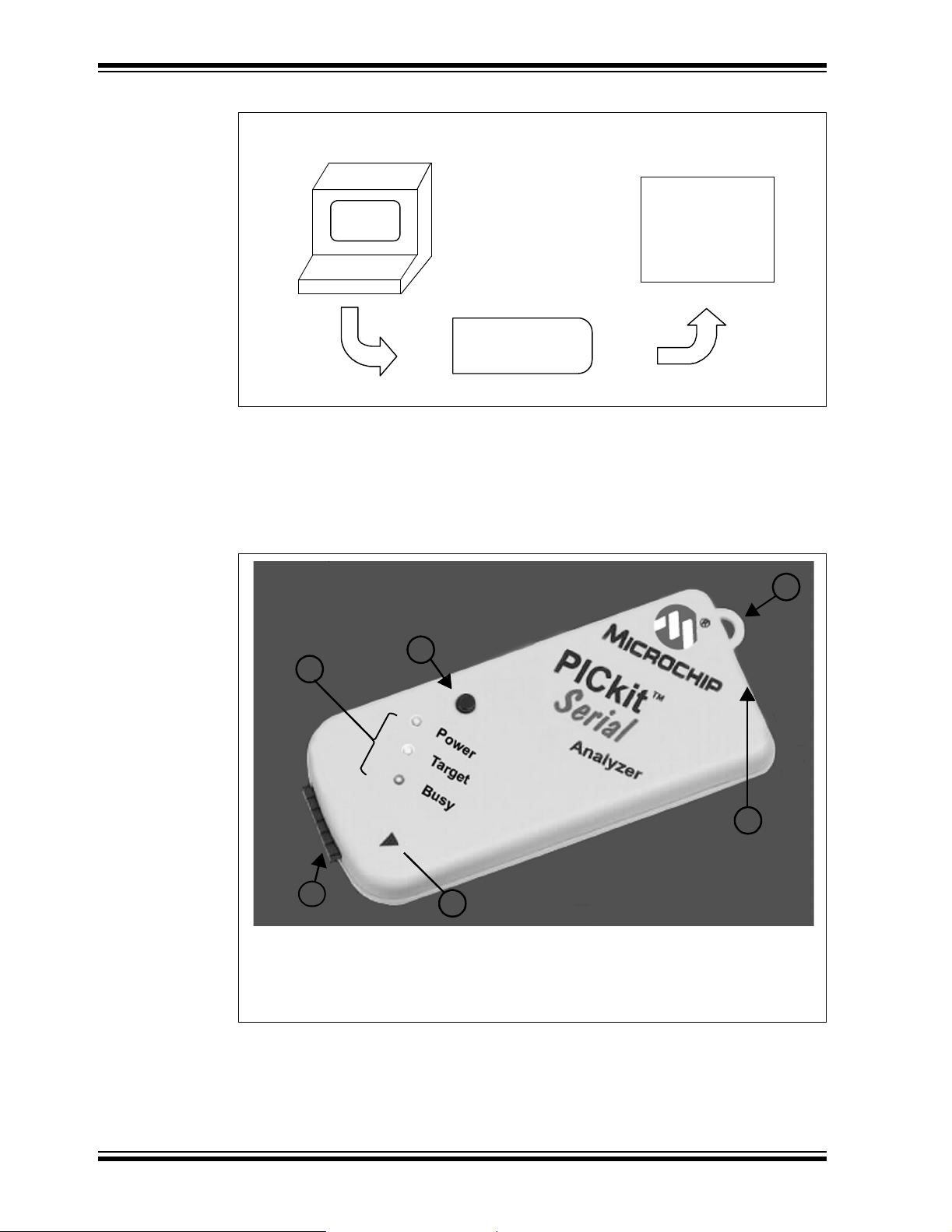
FIGURE 1-1: PICkit™ SERIAL ANALYZER DEVELOPMENT SYSTEM
PC
Target
Device
USB
PICkit™ Serial Analyzer
1.5 PICkit™ SERIAL ANALYZER HARDWARE
The PICkit™ Serial Analyzer connects to a Microsoft® Windows® compatible computer
using a USB port. It interfaces to the target device using a 6-pin header. Figure 1-2
shows an overview of the PICkit™ Serial Analyzer.
FIGURE 1-2: PICkit™ SERIAL ANALYZER
2
1
I2C™
SPI
USART
3
4
6
Legend:
1 – Status LEDs 3 – Lanyard Connection 5 – Pin 1 Marker
2 – Push Button 4 – USB Port Connection 6 – Communications Connector
DS51647A-page 6 © 2007 Microchip Technology Inc.
5
Page 13
PICkit™ Serial Analyzer Overview
1.5.1 Status LEDs
The Status LEDs indicate the status of the PICkit™ Serial Analyzer.
1. Power (green) – Power is applied to the PICkit™ Serial Analyzer by the USB
port.
2. Target (yellow) – The PICkit™ Serial Analyzer is communicating with the target
device.
3. Busy (red) – The PICkit™ Serial Analyzer is communicating with the target
device.
1.5.2 Push Button
The push button is available for future implementation.
1.5.3 Lanyard Connection
To help prevent possible loss of the PICkit™ Serial Analyzer, a convenient lanyard
connection is available.
1.5.4 USB Port Connection
The USB Port Connection is a USB mini-B connector. Connect the PICkit™ Serial
Analyzer to the PC using the supplied cable.
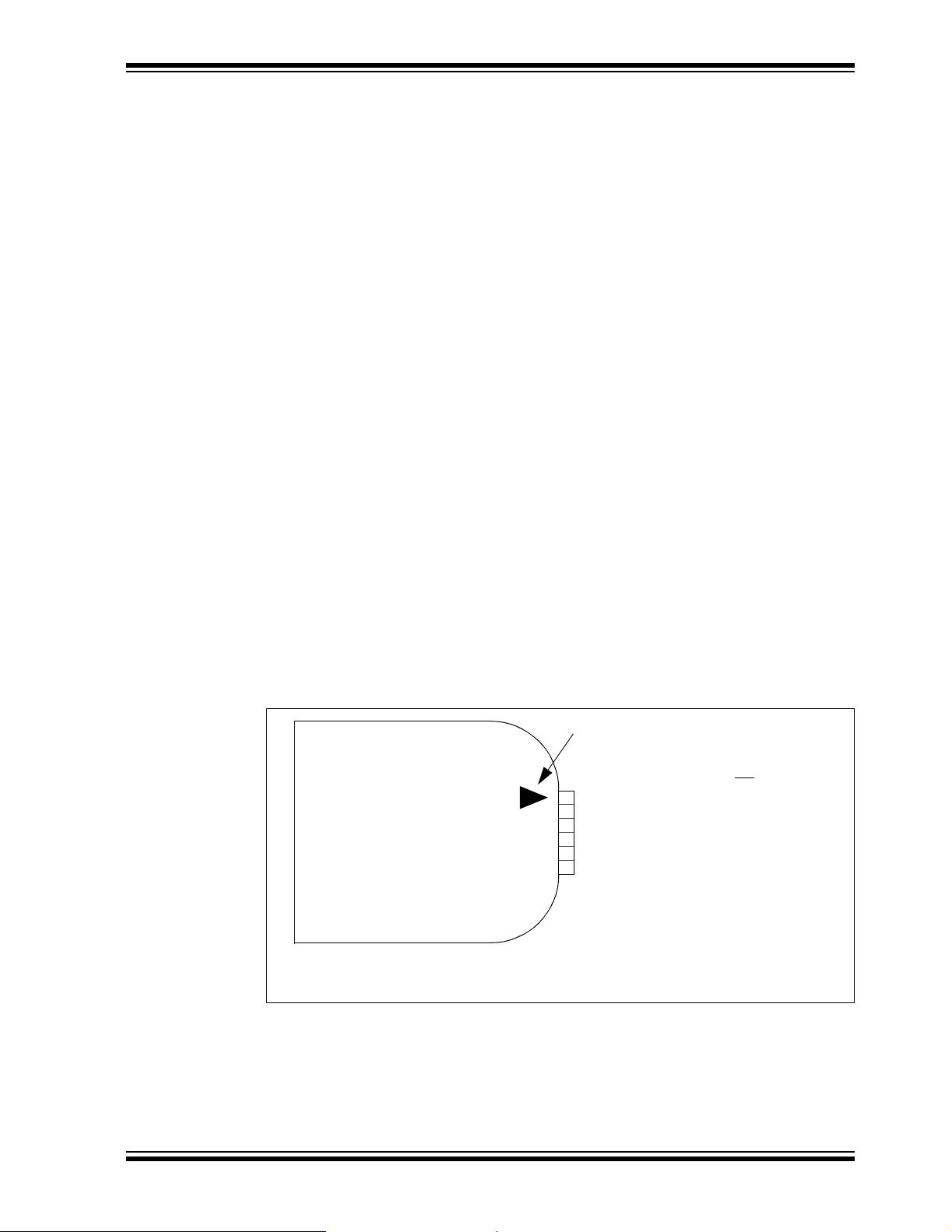
1.5.5 Pin 1 Marker
The Pin 1 marker assists in aligning the PICkit™ Serial Analyzer with the target device.
Pin assignments are shown in Figure 1-3.
1.5.6 Communication Connector
The communication connector connects to the target device using an inexpensive
6-pin, 0.100" pitch spacing, 0.025” square pin header. Pin assignments are shown in
Figure 1-3.
FIGURE 1-3: PICkit™ SERIAL ANALYZER PIN ASSIGNMENTS
Pin 1 Indicator
Pin Description
2
C™ SPI USART
I
1
2
3
4
5
6
1— CS
2+V +V +V
3 GND GND GND
4SDASDI —
5SCLSCK—
6— SDORX
TX
Note: The 6-pin header (0.100" spacing) accepts 0.025" square pins.
© 2007 Microchip Technology Inc. DS51647A-page 7
Page 14
PICkit™ Serial Analyzer User’s Guide
1.6 PICkit™ SERIAL ANALYZER SOFTWARE
1.6.1 PC Program
The PICkit™ Serial Analyzer PC program uses a graphical interface to enter data
and commands to comm unica te to th e target dev ice . Data and c omma nds can be
entered using basic or scr ipting commands. Chapter 3. “PICkit™ Serial Analyzer
PC Program” explains the installation and operation of the program. Following
Chapter 3 there are individual chapters that explain the specific serial communications modes and their operation.
1.6.2 Dynamically Linked Library (DLL)
The PICkit™ Serial Analyzer DLL is explained in Chapter 10. “PICkit™ Serial
Analyzer DLL”.
1.6.3 Firmware
The PICkit™ Serial Analyzer firmware is explained in Chapter 9. “PICkit™ Serial
Analyzer Firmware”.
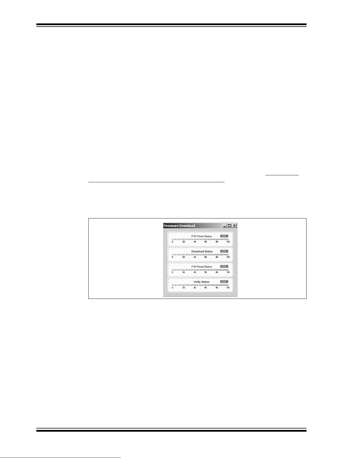
The latest version of the PICkit™ Serial Analyzer firmware can be downloaded from the
Microchip Technology web site. The firmware is updated by selecting PICkit Serial
Analyzer > Download PICkit Serial Analyzer Firmware from the menu bar. An open file
window will open. Select the *.hex file to be uploaded to the PICkit™ Serial Analyzer
and click on the Open button. The Firmware Download window will open as shown in
Figure 1-4 to indicate the status of the firmware update.
FIGURE 1-4: FIRMWARE DOWNLOAD WINDOW
DS51647A-page 8 © 2007 Microchip Technology Inc.
Page 15

2.1 INTRODUCTION
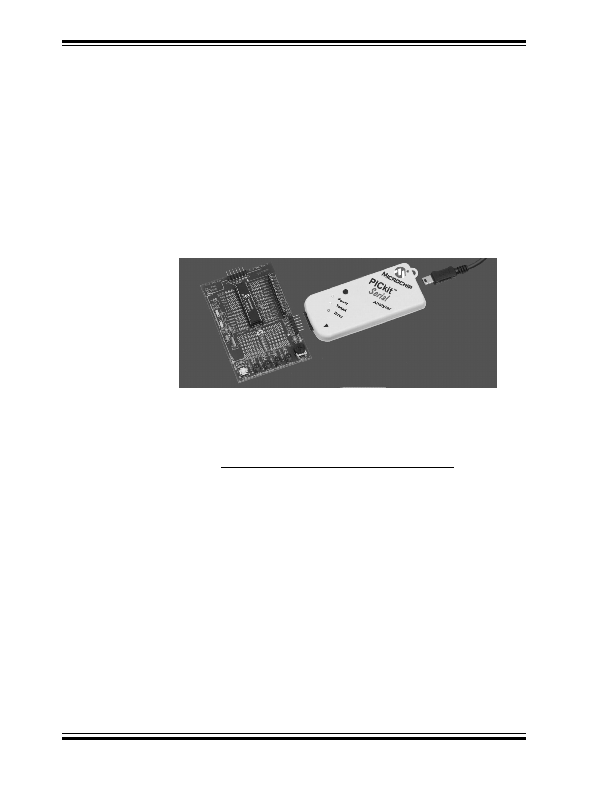
This chapter will get you started using the PICkit™ Serial Analyzer with the 28-Pin
Demo Board. In this demo, the PICkit™ Serial Analyzer will communicate with the
28-Pin Demo Board using the I
2
the I
C Master and the 28-Pin Demo Board will be the I2C Slave device. The 28-Pin
Demo board is programmed to emulate an I
For more information about the 28-Pin Demo Board hardware, see the 28-Pin Demo
Board User’s Guide (DS41 3 01).
For more information about the 28-Pin Demo Board I
Appendix B. “28-Pin Demo Board I
The demo program source code and *.hex file can be found on the PICkit™ Serial
CD-ROM at D:\28-pin Demo Board\Firmware\
2.2 HIGHLIGHTS
This chapter discusses:
• Installing the PICkit™ Serial Analyzer Software
• Connecting the PICkit Serial Analyzer to the PC
• Connecting the PICkit Serial Analyzer to the 28-Pin Demo Board
• Starting the PICkit Serial Analyzer Program
• Running The 28-Pin Demo I
2
•I
C Communications – Basic Operations
• 28-Pin Demo I
PICkit™ SERIAL ANALYZER
Chapter 2. Getting Started
2
C serial protocol. The PICkit™ Serial Analyzer will be
2
C real-time clock and Serial EEPROM.
2
2
C™ Demonstration Firmware”.
.
2
C™ Demonstration Program
2
C™ Source Code and Firmware
C™ demo firmware, see
USER’S GUIDE
2.3 INSTALLING THE PICkit™ SERIAL ANALYZER SOFTWARE
Insert the PICKit™ Serial Analyzer CD-ROM into the CD-ROM drive. In a few moments
the introductory screen should be displayed. Follow the directions on the screen to
install the PICkit Serial Analyzer software.
If the introductory screen does not appear, browse to the CD-ROM directory and select
the AutorunPro.exe program.
Note: The PICkit™ Serial Analyzer program requires the Microsoft
Framework Version 2.0. If the .NET Framework is not installed on your
computer (or if in doubt), select the application plus Microsoft
Framework installation.
®
.NET
®
.NET
2.4 CONNECTING THE PICkit™ SERIAL ANALYZER TO THE PC
Connect the PICkit Serial Analyzer to the PC using the supplied USB cable. There are
no USB drivers to install. The green Power indicator should light indicating that the
PICkit Serial Analyzer is powered.
© 2007 Microchip Technology Inc. DS51647A-page 9
Page 16
PICkit™ Serial Analyzer User’s Guide
2.5 CONNECTING THE PICkit™ SERIAL ANALYZER TO THE 28-PIN DEMO BOARD
Connect the PICkit Serial Analyzer to P3 on the 28-Pin Demo Board as shown in Figure
2-1. The PICkit Serial Analyzer will supply power to the 28-Pin Demo Board and
perform a power on routine:
• LEDs will flash in sequence DS1, DS2, DS3, DS4, DS3, DS2, and DS1 twice
• All LEDs will turn off
• All LEDs will turn on
• All LEDs will turn off
• LEDs will display in hexadecimal: A, D, C
• LEDs will display the top 4 bits of the ADC value read from potentiometer RP1
FIGURE 2-1: CONNECTING PICkit™ SERIAL TO THE 28-PIN DEMO
BOARD
2.6 STARTING THE PICkit™ SERIAL ANALYZER PROGRAM
You can start the program by:
• Clicking on the desktop icon, or
• Navigating to Start>All Pr ograms>Microchip>PICkit Serial Analyzer
After a few moments, the program will start and display the main window as shown in
Figure 2-2.
If this is the first time you are running the program, the Configuration Wizard will auto-
matically run. Click on the Next button and accept the default settings for I
mode. For more information about using the I
Master Communications.”
2
C Master mode, see Chapter 4. “I2C™
2
C Master
DS51647A-page 10 © 2007 Microchip Technology Inc.
Page 17
Getting Started
FIGURE 2-2: PICkit™ SERIAL ANALYZER MAIN WINDOW
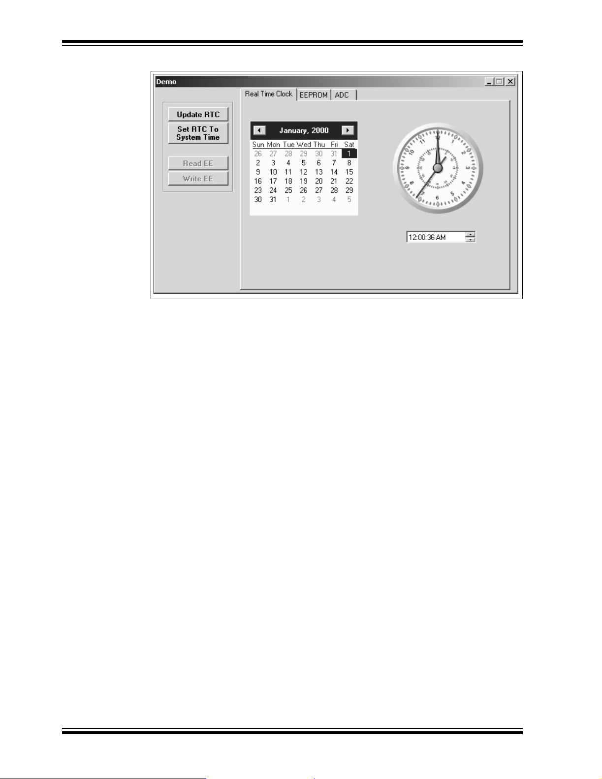
2.7 RUNNING THE 28-PIN DEMO I2C™ DEMONSTRATION PROGRAM
Select the 28-Pin Demo I2C demonstration by clicking on Demo Boards > 28 Pin Demo
I2C from the menu bar. The 28-Pin Demo I2C demonstration window will be displayed
as shown in Figure 2-3.
The Real-Time Clock (RTC) will be displayed first. Note the tabs to select between the
RTC, EEPROM and ADC demonstrations. The demonstration program will constantly
poll the 28-Pin Demo Board and display the contents of the real-time clock and the
ADC.
2.7.1 Real-Time Clock (RTC)
Clicking on the Real-Time Clock tab will display calendar and clock contents of the
real-time clock function running on the 28-Pin Demo Board. The 28-Pin Demo Board
has been programmed to emulate a stand-alone serial I
2
I
C commands are very similar to the commands used in these devices. The demonstration program will constantly poll the 28-Pin Demo Board and display the contents
of the real-time clock.
The Real-Time Clock window displays calendar and clock controls. Notice the date and
time when the 28-Pin Demo Board has first been powered on. The date and time start
at January 1, 2000 at midnight (12:00 AM).
The user can manually enter calendar and clock values and send the values to the
real-time clock by clicking on the Update RTC button. Or the user can click on the Set
RTC to System Time button to set the real-time clock to the date and time of the
computer.
2
C clock-calendar device. The
© 2007 Microchip Technology Inc. DS51647A-page 11
Page 18
PICkit™ Serial Analyzer User’s Guide
FIGURE 2-3: 28-PIN DEMO I2C™ – RTC
2.7.2 Serial EEPROM (EEPROM)
Clicking on the EEPROM tab will display the 256 byte array of EEPROM memory as
shown in Figure 2-4. The 28-Pin Demo Board has been programmed to emulate a
stand-alone serial I
very similar to the commands used in these devices.
The Serial EEPROM tab displays the contents of a serial EEPROM implemented on
the 28-Pin Demo Board. When this tab is first displayed, the values are grayed out. This
means that the display does not match the contents of the emulated serial EEPROM.
Click on Read EE button and the program will read and display the contents of the
28-Pin Demo Board. Notice that the displayed values are now black.
Individual memory locations can be changed by clicking on the value and typing in a
new value in hexadecimal. Notice that the changed values will be displayed in red. This
means the value has changed but has not been written to the emulated serial
EEPROM. Click on the Write EE button and the values will be written. The color of the
value will turn to black indicating that the value has been written and the display
matches the contents of the emulated serial EEPROM.
2
C EEPROM device such as a 24LC02. The I2C commands are
DS51647A-page 12 © 2007 Microchip Technology Inc.
Page 19
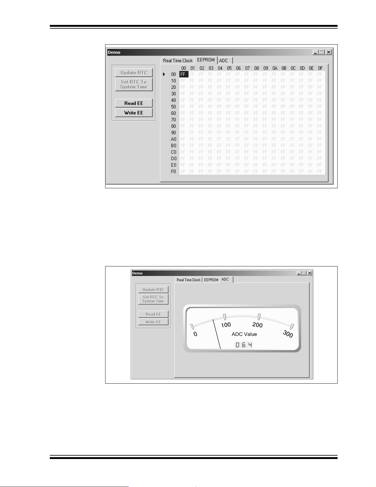
FIGURE 2-4: 28-PIN DEMO I2C™ – EEPROM
Getting Started
2.7.3 Analog-to-Digital Converter (ADC)
Clicking on the ADC tab will show a meter gauge displaying the value of the ADC as
read from potentiometer RP1 as shown in Figure 2-5.
The meter gauge displays the Most Significant 8 bits of the 10-bit ADC internal to the
®
PIC
microcontroller. Rotate potentiometer RP1 and the display changes almost
instantaneously. The demonstration program will constantly poll the 28-Pin Demo
Board and display the contents of the ADC.
FIGURE 2-5: 28-PIN DEMO I
2
C™ – ADC
© 2007 Microchip Technology Inc. DS51647A-page 13
Page 20
PICkit™ Serial Analyzer User’s Guide
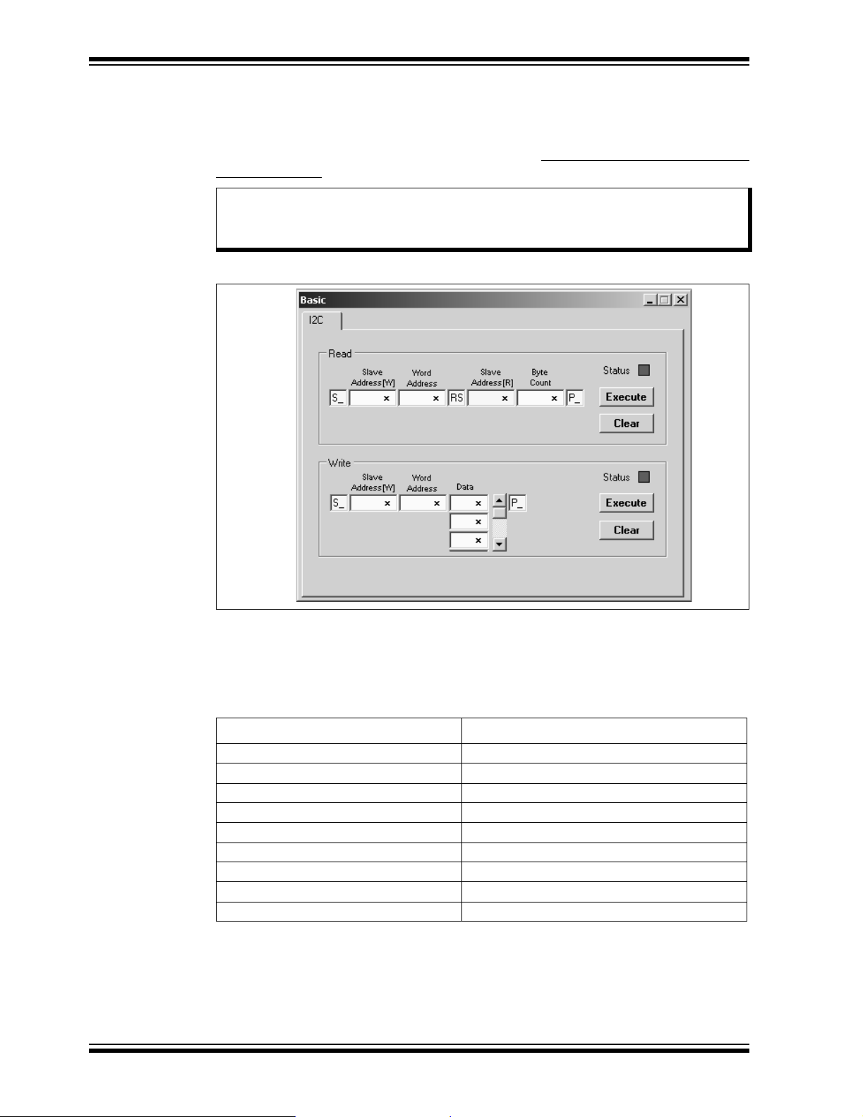
2.8 I2C™ COMMUNICATIONS – BASIC OPERATIONS
Individua l I2C commands and data can be read and written to the 28-Pin Demo Board
from the Basic Operations window as shown in Figure 2-6. Ensure that the PICkit Serial
Analyzer program is in I
figuration Wizard from the menu bar and selecting I2C Master.
2
C Master mode by selecting PICkit Serial Analyzer > Run Con-
Note: The 28-Pin Demo I
opened at the same time. When the 28-Pin Demo I
the Basic Operations window will automatically close.
FIGURE 2-6: I
2
C™ BASIC OPERATIONS
2
C window and the Basic Operations window cannot be
2
C window is opened,
2.8.1 Real-Time Clock (RTC)
The Slave address for the emulated real-time clock on the 28-Pin Demo Board is
hexadecimal A2 (0xA2). The Word Address selects the following memory locations:
TABLE 2-1: MEMORY LOCATIONS
Word Address Contents
0x00 Configuration 1
0x01 Configuration 2
0x02 Seconds
0x03 Minutes
0x04 Hours
0x05 Days
0x06 Weekdays
0x07 Months
0x08 Years
DS51647A-page 14 © 2007 Microchip Technology Inc.
Page 21
Getting Started
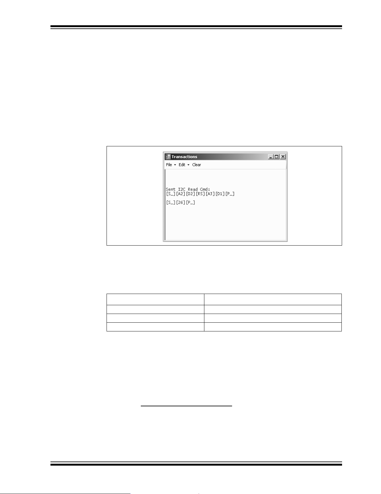
For example, to read seconds from the real-time clock:
Step 1 – Enter 0xA2 into the Slave Address[W] block in the Read section of the Basic
Operations window (top half of window)
Step 2 – Enter 0x02 into the Word Address block
Step 3 – Note that the Slave Address[R] has already been entered for you (the Read
bit is set).
Step 4 – Enter 0x01 into the Byte Count block
Step 5 – Click on the Execute button
2
The I
C combination command (Write then Read) will be sent to the 28-Pin Demo
Board. The command and the contents of Word Address 0x02 (seconds) will be
displayed in the transaction window as shown in Figure 2-7.
FIGURE 2-7: RTC TRANSACTIONS DEMO
2.8.2 EEPROM
The Slave address for the emulated Serial EEPROM on the 28-Pin Demo Board is
hexadecimal A8 (0xA8). The Word Address selects one of 256 8-bit memory locations:
TABLE 2-2: WORD ADDRESS CONTENTS
Word Address Contents
0x00 Memory Contents
… …
0xFF Memory Contents
2.8.3 ADC
The Slave address for the ADC on the 28-Pin Demo Board is hexadecimal AA (0xAA).
The Word Address 0x01 selects the memory location containing the Most Significant 8
bits of the 10-bit ADC of the PIC microcontroller.
2.9 28-PIN DEMO I2C™ SOURCE CODE AND FIRMWARE
The demo program source code and *.hex file can be found on the PICkit Serial
CD-ROM at D:\28-pin Demo Board\Firmware\
.
© 2007 Microchip Technology Inc. DS51647A-page 15
Page 22

PICkit™ Serial Analyzer User’s Guide
NOTES:
DS51647A-page 16 © 2007 Microchip Technology Inc.
Page 23

PICkit™ SERIAL ANALYZER
USER’S GUIDE
Chapter 3. PICkit™ Serial Analyzer PC Program
3.1 INTRODUCTION
This chapter covers the installation, starting and high level operations of the PICkit
Serial Analyzer program. Detailed information about the entering of data and commands for specific serial communications modes are given in the following chapters.
3.2 HIGHLIGHTS
This chapter discusses:
• Installing The PICkit Serial Analyzer Software
• Starting the Program
• Configuration Wizard
• Main Window
• Specific Communications Modes
3.3 INSTALLING THE PICkit™ SERIAL ANALYZER SOFTWARE
Insert the PICKit Serial Analyzer CD-ROM into the CD-ROM drive. In a few moments
the introductory screen should be displayed. Follow the directions on the screen to
install the PICkit Serial Analyzer software.
If the introductory screen does not appear, browse to the CD-ROM directory and select
the AutorunPro.exe program.
Note: The PICkit Serial Analyzer program requires the Microsoft
Framework Version 2.0.
3.4 STARTING THE PROGRAM
You can start the program by
• Clicking on the desktop icon, or
• Navigating to Start>All Pr ograms>Microchip>PICkit Serial Analyzer
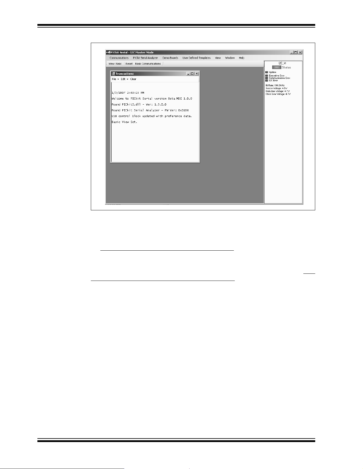
After a few moments, the program will start and display the main window as shown in
Figure 3-1.
®
.NET
© 2007 Microchip Technology Inc. DS51647A-page 17
Page 24
PICkit™ Serial Analyzer User’s Guide
FIGURE 3-1: PICkit™ SERIAL ANALYZER MAIN WINDOW
3.5 CONFIGURATION WIZARD
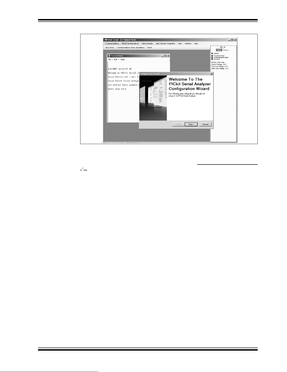
If it is the first time that the PICkit Serial Analyzer program is run, the Configuration Wizard will run automatically . The Configuration Wizard can be manually invoked by selecting PICkit Serial Analyzer > Run Configuration Wizard
The Configuration Wizard will guide you through the basic steps to configure the PICkit
Serial Analyzer program for a specific communications mode (I
Advanced configuration can be done from the Configuration Window by selecting PIC-
kit Serial Analyzer > Configure Communications Mode from the menu bar.
As an example, Figure 3-2 through Figure 3-7 show how to configure for I
mode. Refer to the specific communications chapter for detailed information on the
Configuration Wizard for that communications mode.
The Configuration Wizard Welcome window is shown in Figure 3-2. You may choose
to continue by clicking on the Next button or canceling the wizard by clicking on the
Cancel button.
from the menu bar.
2
C, SPI, USART).
2
C Master
DS51647A-page 18 © 2007 Microchip Technology Inc.
Page 25
PICkit™ Serial Analyzer PC Program
FIGURE 3-2: CONFIGURATION WIZARD – WELCOME
The Configuration Wizard Page 1 of 4, as shown in Figure 3-3, displays the available
communications modes and allows you to choose one of the modes.
FIGURE 3-3: CONFIGURATION WIZARD – PAGE 1 OF 4
In this example, I
2
C Master Communication’s mode is selected. The Configuration
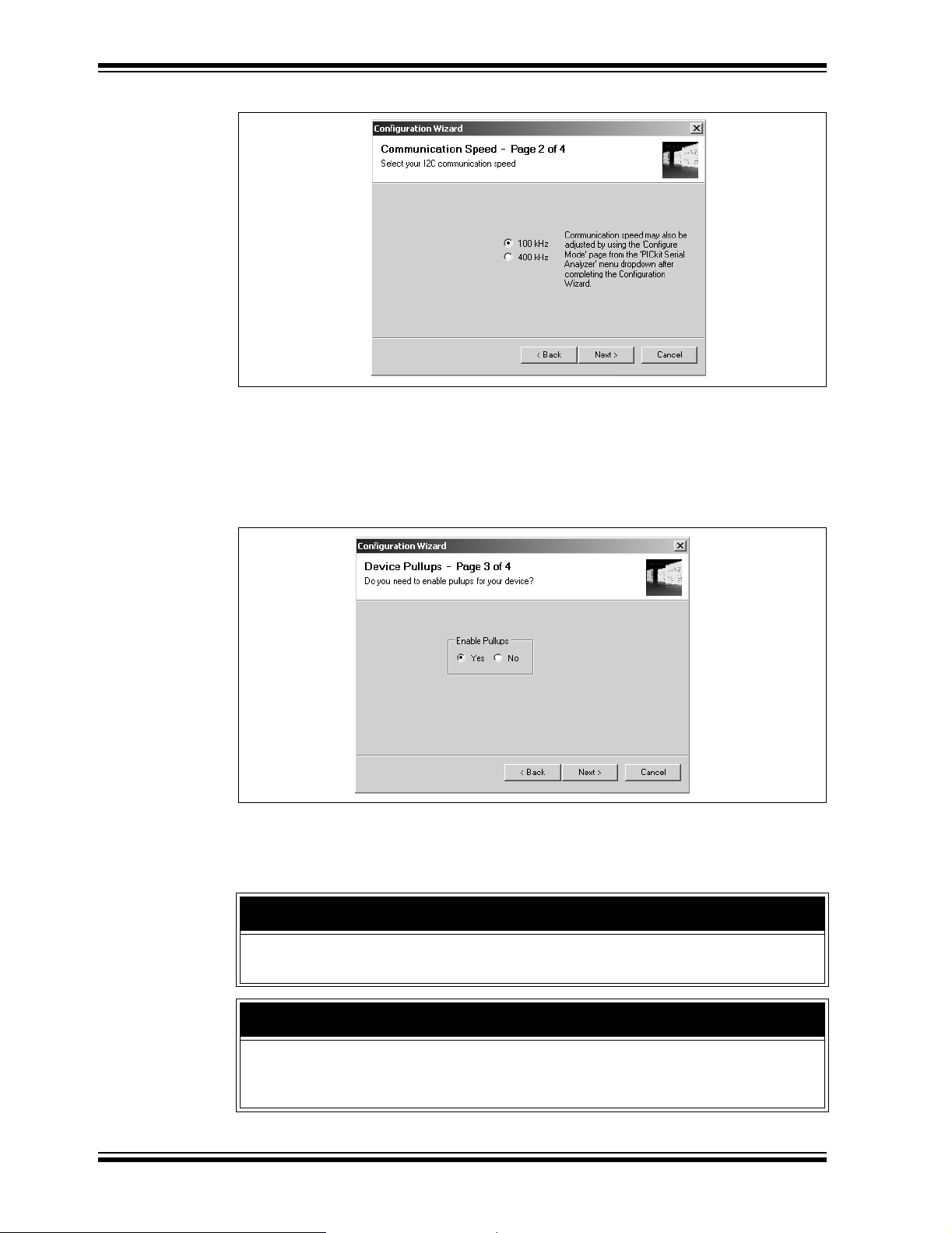
Wizard Page 2 of 4, as shown in Figure 3-4, allows you to select the bus speed. A more
comprehensive list of bus speeds can be chosen from the Configuration Window by
selecting PICkit Serial Analyzer > Configure Communications Mode
© 2007 Microchip Technology Inc. DS51647A-page 19
from the menu bar.
Page 26
PICkit™ Serial Analyzer User’s Guide
FIGURE 3-4: CONFIGURATION WIZARD – PAGE 2 OF 4
2
C bus requires pull-up resistors. The PICkit Serial Analyzer has the ability to
The I
enable internal 2.2 kΩ pull-up resistors. If the target device does not have pull-up resistors installed, then enable pull-ups by selecting the Yes radio button as shown in
Figure 3-5. If the target device has the pull-up resistors installed, you can disable the
internal pull-ups by selecting the No radio button.
FIGURE 3-5: CONFIGURATION WIZARD – PAGE 3 OF 4
The PICkit Serial Analyzer can power the target device from 0 to 5 V
total current limit of 100 mA (PICkit Serial Analyzer plus target device). The Configuration Wizard Page 4 of 4, as shown in Figure 3-6, allows you to choose between
powering the target device and selecting the specific target voltage.
DC at a combined
CAUTION
Even though the voltage can be set as low as 0 VDC, it is up to the user to verify the
required operating voltage of the target device.
CAUTION
The USB port current limit is set to 100 mA. If the target plus PICkit Serial Analyzer
exceeds this current limit, the USB port will turn off. The target may be powered
externally if more power is required.
DS51647A-page 20 © 2007 Microchip Technology Inc.
Page 27

PICkit™ Serial Analyzer PC Program
FIGURE 3-6: CONFIGURATION WIZARD – PAGE 4 OF 4
Once all pages of the Configuration Wizard are completed, you can choose to not
display the wizard at start up by checking the Do not show this wizard on start-up again
check box.
FIGURE 3-7: CONFIGURATION WIZARD – Y OU’RE DONE!
3.6 MAIN WINDOW
3.6.1 Menu Bar
The menu bar selects various functions of the PICkit Serial Analyzer program. A
summary of the functions are:
FIGURE 3-8: MENU BAR
Menu Bar
© 2007 Microchip Technology Inc. DS51647A-page 21
Page 28

PICkit™ Serial Analyzer User’s Guide
COMMUNICATIONS
The Communications menu selections display operation windows to enter data and
commands to communicate with the target device.
• Basic Operations
mode selected (see PICkit Serial Analyzer -> Select Communications Mode)
•Script
PICkit™ SERIAL ANALYZER
The PICkit Serial Analyzer menu selection commands the PICkit Serial Analyzer
hardware.
• Select Communications Mode
• Configure Communications Mode
• Download PICkit Serial Analyzer Firmwa re
• Run Configuration Wizard
• Perform Syste m Reset
• Reset PICkit Serial Analyzer
• PICkit Serial Analyzer No.
>
- Script Builder
- Script Execute
2
-I
C Master – Puts the PICkit Serial Anal yzer in I2C Master Communications
mode
-SPI Master
mode
- USART Asynchronous
nous Communications mode
- USART Synchronous Master
Synchronous Master Communications mode
Mode window for the communications mode selected (see PICkit Serial Analyzer
-> Select Communications Mode)
window. Firmware updates are available from the Microchip Technology web site.
PICkit Serial Analyzer
condition is present
from the PC software. The number is assigned to the hardware as it enumerates
on the USB bus.
– Displays the Basic Operations window for the communications
– Displays the Script Builder window
– Displays the Script Execute window
>
– Puts the PICkit Serial Analyzer in SPI Master Communications
– Puts the PICkit Serial Analyzer in USART Asynchro-
– Puts the PICkit Serial Analyzer in USART
– Displays the Configuration Communications
– Displays the Firmware Download
– Displays the Configurat ion Wizard
– Closes and then reinitializes USB communications to the
– Resets the PICkit Serial Analyzer if an error
– Up to four PICkit Serial Analyzers can be controlled
DEMO BOARDS
The Demo Boards menu selection displays the selected demonstration window. The
PICkit Serial Analyzer program will be automatically configured for the communications
mode of the selected demonstr ation.
•28
-Pin Demo I2C – Displays the 28-Pin Demo Board I2C demo graphical user
interface. For more informati on se e Appendix B. “28-Pin Demo Board I
Firmware.”
USER DEFINED TEMPLATES
• Create Template
•My Templates
VIEW
•Basic
DS51647A-page 22 © 2007 Microchip Technology Inc.
– The PICkit Serial Analyzer program will display basic commands and
status view
– Displays the Parameter Template creation window
– Selects and displays template windows created by the user
2
C™
Page 29
PICkit™ Serial Analyzer PC Program
• Advanced – The PICkit Serial Analyzer program will display advanced commands
and status view
WINDOW
• New Transaction Window
transaction windows can be opened as needed for logging communications.
•Close All
• Cascade
• Tile Horizontally
• Tile Vertically
HELP
• About
• Show PICkit Serial Analyzer Connections
communications mode
• Show Even t By tes
– Closes all windows
– Cascade windows
– Tile windows horizontally
– Tile windows vertically
– Displays program version information
– Displays Event Marker code for current communication mode
– Opens new or additional transaction window. Multiple
– Displays pinout for current
3.6.2 Tool Bar
FIGURE 3-9: TOOL BAR
Tool Bar
The Tool Bar gives quick access to often used commands. These commands are also
available from the Menu Bar.
•View: Basic
• Reset
• Basic Communications
communications mode selected
/Advanced – toggles between Basic and Advanced views
– Resets the PICkit Serial Analyzer if an error condition is present
– Displays the Basic Operations window for the
3.6.3 Status Col umn
The Status Column displays status information for the selected serial communications
mode. In Ba sic V iew m ode, a simpl ified st atus i s disp layed a s show n in Fi gure 3-10. In
Advanced View mode additional status information is displayed for the communications
mode selected as shown in Figure 3-11.
The status information that is displayed depends on the selected communications
mode (I
status window for the particular serial communications mode.
2
C, SPI, USART). The following chapters give more detailed explanation of the
© 2007 Microchip Technology Inc. DS51647A-page 23
Page 30
PICkit™ Serial Analyzer User’s Guide
FIGURE 3-10: STATUS COLUMN (BASIC VIEW)
FIGURE 3-11: STATUS COLUMN (ADVANCED VIEW)
Status Column
Status Column
3.6.4 Tr ansactions Window
The Transactions window, shown in Figure 3-12, keeps a running log of the commands
and data that are communicated between the PICkit Serial Analyzer program and
target device.
From the menu bar on the Transaction window, the contents can be saved (File>Save
to a *.txt or *.rtf file. The file can later be retrieved (File>Open
Transactions window.
Additional Transactions windows can be displayed. From the PICkit Serial Analyzer
menu bar , sel ect Window > New Transaction Window
will log the current commands and data.
DS51647A-page 24 © 2007 Microchip Technology Inc.
. The active Transactions window
) and displayed in the
)
Page 31

PICkit™ Serial Analyzer PC Program
FIGURE 3-12: TRANSACTIONS WINDOW
Transactions Window
FILE
• Open
•Save
•Close
– Opens a *.txt or *.rtf file and displays it in the Transactions window
– Saves the contents of the Transactions window to a *.txt or *.rtf file
– Closes the selected Transactions window
EDIT
•Copy
– The selected contents of the Transactions window will be copied to the
clipboard
•Paste
•Select
•Clear All
– The contents of the clipboard will be pasted into the Transactions window
All – contents of the Transactions window will be selected
– The contents of the Transactions window will be cleared
The Transaction window also allows usage of the common keyboard shortcuts Ctrl-X,
Ctrl-C, Ctrl-V to cut, copy and paste from the clipboard.
CLEAR – The contents of the Transactions window will be cleared
3.7 SERIAL COMMUNICATIONS MODES
Detailed information about the entering of data and commands for specific serial
communications modes are given in the following chapters.
© 2007 Microchip Technology Inc. DS51647A-page 25
Page 32

PICkit™ Serial Analyzer User’s Guide
NOTES:
DS51647A-page 26 © 2007 Microchip Technology Inc.
Page 33

Chapter 4. I2C™ Master Communications
4.1 INTRODUCTION
This chapter describes the I2C Master Communications mode. I2C data and
commands can be entered using a Basic Communications window or by creating Script
Commands.
It is assumed that the user is familiar with the I
• The I
Semiconductor (formerly Philips Semiconductor) web site at
http://www.nxp.com/acrobat_download/literature/9398/39340011.pdf
2
•An I
web site. Click on the links: Support -> Getting Started -> PIC MCU Tutorials ->
I2C Master Mode
• Several application notes are available on the Microchip Technology web site.
Click on links: Design -> App Notes -> Function: Communications -> I2C
4.2 HIGHLIGHTS
PICkit™ SERIAL ANALYZER
USER’S GUIDE
2
C protocol . For more information see:
2
C-Bus Specification Version 2.1 January 2000 is available from NXP
C Master Communications tutorial is available on the Microchip Technology
This chapter discusses:
• PICkit Serial Pin Assignments
• Selecting Communications Mode
• Configuring I
• Communications: Basic Operations
• Script Builder
• Script Execute
2
C Communications Mode
4.3 PICkit SERIAL PIN ASSIGNMENTS
The PICkit Serial Analyzer pin assignments for I2C Master mode are:
TABLE 4-1: PIN ASSIGNMENTS
Pin Label Type Description
1 AUX1 Input/Output Auxiliary I/O port pin No. 1
2 +V Power Target Power
3 GND Power Ground
4 SDA Input/Output Serial Data
5 SCL Power Serial Clock
6 AUX2 Input/Output Auxiliary I/O port pin No. 2
4.4 SELECTING COMMUNICATIONS MODE
The I2C Master Communications mode is selected from the Configuration Wizard or
menu bar.
Configuration Wizard – Select PICkit Serial Analyzer > Run Configuration Wizard
from the menu bar
© 2007 Microchip Technology Inc. DS51647A-page 27
Page 34

PICkit™ Serial Analyzer User’s Guide
Menu Bar – Select PICkit Serial Analyzer > Select Communications Mode > I2C
Master
4.5 CONFIGURING I2C COMMUNICATIONS MODE
Once the communications mode has been selected, it is configured from the Configuration Wizard or menu bar.
Configuration Wizard – Select PICkit Serial Analyzer > Run Configuration Wizard
from the menu bar
Menu Bar – Select
The Configure Mode window will open. Depending on the View selected, the Basic
View (Figures 4-1) displays a minimum choice of configurations commands. In the
Advanced View (Figures 4-2) displays an extended choice of configuration commands.
Save the configuration by clicking on the Save Changes button.
PICkit Serial Analyzer > Configure Communications Mode
FIGURE 4-1: I
OPTIONS
• Enable Event Markers
• Enable Time Markers
• Enable Pull
tion lines
VOLTAGE
-ups – Enable internal 2.2 kΩ pull-ups on SDA and SCL communica-
2
C™ CONFIGURE COMMUNICATIONS MODE – BASIC VIEW
– Enable event markers
– Enable ‘time’ stamp to accompany all event markers
• PICkit Serial will power my device
power the target device. The target can be powered at 5 V
variable voltage.
– Select the check box if the PICkit Serial will
DC or a user selectable
CAUTION
Even though the voltage can be set as low as 0 VDC, it is up to the user to verify the
required operating voltage of the target device.
CAUTION
The USB port current limit is set to 100 mA. If the target plus PICkit Serial Analyzer
exceeds this current limit, the USB port will turn off. The target may be powered
externally if more power is required.
DS51647A-page 28 © 2007 Microchip Technology Inc.
Page 35

I2C™ Master Communications
COMM I2CM BIT RATE
Select the desired I2C bus bit rate using the drop down box.
FIGURE 4-2: I
EVENT MARKERS
•Abrt Mac Exe
• Macro Loop
• Mac Lp 65536
• Mac Lp Done
• Timeout Timer1
• Timeout Timer2
• Status Error
– Enable event marker: abort ‘macro’ execution
– Enable event marker: top of ‘macro’ loop
– Enable event marker: ‘macro’ loop count overflow (i.e., 65536)
– Enable event marker: ‘macro’ loop iterations complete
– Enable event marker: Timer1 expired
– Enable event marker: Timer2 expired
– Enable event marker: change in status byte
2
C™ CONFIGURE COMMUNICATIONS MODE – ADVANCED
VIEW
•Start Bit
• Stop Bit
•Restart Bit
• Ack/Nack TX
• Ack/Nack RX
• Write Byte
• Read Byte
•TX Error
• Status Error
ADVANCED OPTIONS
• Disable LED2 Default
LED)
• Disable LED1 Default
• Enable Switch Test
- Switch Off (not depressed) – blink LED1, LED2 off
- Switch ON (depressed) – blink LED2, LED1 off
• AUX1 Default State
• AUX2 Default State
•AUX1 Direction
– Enable event marker – Start bit
– Enable event marker – Stop bit
– Enable event marker – Restart bit
– Enable event marker – Ack or Nack byte transmit
– Enable event marker – Ack or Nack byte received
– Enable event marker – write byte
– Enable event marker – read byte
– Enable event marker – TX error
– Enable event marker – change in I2C status byte
– Disable default LED2 behavior (LED2 = Yellow ‘Target’
– Disable default LED1 behavior (LED1 = Red ‘Busy’ LED)
– Enable low level switch test:
– AUX1 communication line – default state (0 | 1)
– AUX2 communication line – default state (0 | 1)
– AUX1 communication line – direction: 1: input, 0: output
© 2007 Microchip Technology Inc. DS51647A-page 29
Page 36

PICkit™ Serial Analyzer User’s Guide
• AUX2 Direction – AUX2 communication line – direction: 1: input, 0: output
4.6 COMMUNICATIONS: BASIC OPERATIONS
The I2C Basic Operations window can be opened by selecting:
• Communications: Basic Operations
• Communications > Basic Operations
2
The I
C Basic Operations window is shown in Figures 4-3. There are two basic
communications commands, Read and Write.
Read performs a combination Write then Read commands to the target device (refer to
2
the I
C Specification reference in Section 4.1 “Introduction” above). The basic
structure of the command is:
• Start bit (S_)
• Slave Address[W] – Enter the slave address of the device to communicate with.
The write bit should be cleared to indicate a write operation
• Word Address – Enter the word address
• Restart (RS),
• Slave Address[R] – The slave address with the write bit set will be automatically
entered when the Slave Address[W] has been entered
• Byte Count – Enter the number of bytes to be read
• Stop bit (P_)
from the tool bar, or
from the menu bar
Note: The “x” indicates the value is a hexadecimal number. Clicking on “x” will
toggle it to a “d” indicating that the value is a decimal number.
Write performs a write operation to the target device (refer to The I
reference in Section 4.1 “Introduction” above). The basic structure of the command
is:
• Start bit (S_)
• Slave Address[W] – Enter the slave address of the device to communicate with.
The write bit should be cleared to indicate a write operation.
• Word Address – Enter the word address
• Data – Enter up to eight bytes of data
• Stop bit (P_)
The command will be logged in the Transactions window. A listing of the command
abbreviations is given in Table 4-2.
2
C Specification
DS51647A-page 30 © 2007 Microchip Technology Inc.
Page 37

FIGURE 4-3: I2C™ BASIC OPERATIONS
4.7 SCRIPT BUILDER
I2C commands can be combined into scripts, saved, and used over again. The Script
Builder window is opened by selecting Communications > Script > Script Builder
the menu ba r. The Script Builder is shown in Figures 4-4.
The Script Builder window is divided into four columns as shown in Figures 4-5 through
4-8.
I2C™ Master Communications
from
FIGURE 4-4: I
2
C™ SCRIPT BUILDER
4.7.1 Script Commands
The left most column contains the Script Commands as shown in Figures 4-5.
•Script Name
• Save Script
• Execute Script
column
•Clear Script
• Del User Scripts
•Show Array
may be entered. This data can be included in the script by right clicking in a Script
Detail cell and choosing “Insert Array”.
– Enter the name of the script
– Saves the script
– Executes (performs) the script displayed in the Script Detail
– Clears the Script Detail column
– Deletes scripts from the User Scripts column.
– Displays a spreadsheet-like table in which large amounts of data
© 2007 Microchip Technology Inc. DS51647A-page 31
Page 38

PICkit™ Serial Analyzer User’s Guide
FIGURE 4-5: I2C™ SCRIPT BUILDER – SCRIPT COMMANDS
Script Commands
4.7.2 Example Scripts
The second column contains Example Scripts as shown in Figures 4-6. These can be
studied to learn how to create or to edit custom scripts. T o load the example script into
the Script Detail column, either double click or right click and select from the local
menu.
FIGURE 4-6: I
2
C™ SCRIPT BUILDER – EXAMPLE SCRIPTS
Example Scripts
4.7.3 Script Detail
The third column contains Script Detail as shown in Figures 4-7. This column is used
to create the script or view an existing script. More information about creating a custom
script is discussed in Section 4.7.5 “Creating A Script”.
To load a user script from the User Scripts column into the Script Detail column, the
user can double click or right click and select from the local menu.
Note: The “x” indicates the value is a hexadecimal number. Clicking on “x” will
toggle it to a “d” indicating that the value is a decimal number.
DS51647A-page 32 © 2007 Microchip Technology Inc.
Page 39

I2C™ Master Communications
FIGURE 4-7: I2C™ SCRIPT BUILDER – SCRIPT DETAIL
Script Detail
4.7.4 User Scripts
The fourth column contains User Scripts as shown in Figures 4-8. User scripts that are
created, n amed, and saved are displayed in the User Scripts column.
To load a user script from the User Scripts column into the Script Detail column, the
user can double click or right click and select from the local menu.
User Scripts can be deleted by right clicking and selecting Delete Script from the local
menu.
FIGURE 4-8: I
2
C™ SCRIPT BUILDER – USER SCRIPTS
User Scripts
4.7.5 Creating A Script
Scripts are created by placing the cursor into the Script Detail column and right clicking.
A local menu will be displayed as shown in Figures 4-9. Select from the choice of
commands or script macro commands.
The sequence of macro commands are executed from top to bottom. Macro commands
are entered by right clicking in the box and selecting from the local menu as shown in
Figures 4-9.
© 2007 Microchip Technology Inc. DS51647A-page 33
Page 40

PICkit™ Serial Analyzer User’s Guide
Macro commands are entered according to the sequence of events as defined by the
2
I
C bus protocol. Studying the example scripts is a good way to learn the sequence of
events. The example scripts can also be modified and saved under a different name.
CAUTION
The choice of macro commands is very flexible. Therefore, the correctness of the
script has to be verified by the user. The PICkit Serial Analyzer program does not
verify the correctness of the script.
A complete listing of the available macro commands is given in Table 4-2. The macro
command abbreviation will be displayed in the Transactions Window. The Transactions
window keeps a running log of the commands and data sent to and from the target
device.
FIGURE 4-9: I
2
C™ SCRIPT BUILDER – CREATING A SCRIPT
TABLE 4-2: I2C™ SCRIPT MACRO COMMAND
Macro Command
I2CINIT [I_] I
I2CSTART [S_] I2C™ Start
I2CSTOP [P_] I2C™ Stop
I2CRESTART [RS] I2C™ Restart
I2CWRTBYT [W_] I2C™ Write Bytes. Next byte is the byte count,
I2CRDBYT [R_] I2C™ Read Bytes. Next byte is the byte count.
I2CRDBLK [RB] I2C™ Read Block
I2CBITRATE [BR] Set I2C™ Bit Rate - min:0 = 35k, ma x:127 = 100k.
I2CRESET [RE] Reset MSSP module
I2CRDBYTNLB [RN] Read bytes - NACK last byte. Next byte is the byte
I2CRDBLKNLB [RBN] Read block - NACK last byte
I2CAUX1RST [A1RST] Reset AUX1
Command
Abbreviation
Description
2
C™ Initialization
followed by the data.
Next byte is the bit rate.
count
DS51647A-page 34 © 2007 Microchip Technology Inc.
Page 41

TABLE 4-2: I2C™ SCRIPT MACRO COMMAND (CONTINUED)
I2CAUX1SET [A1RST] Set AUX1
I2CAUX1OUT [A1OUT] Set AUX1 direction to Output
I2CAUX1IN [A1IN] Set AUX1 direction to Input
I2CAUX1W0 [A1W0] AUX1 Wait 0
I2CAUX1W1 [A1W1] AUX1 Wait 1
I2CAUX2RST [A2RST] Reset AUX2
I2CAUX2SET [A2RST] Set AUX2
I2CAUX2OUT [A2OUT] Set AUX2 direction to Output
I2CAUX2IN [A2IN] Set AUX2 direction to Input
I2CAUX2W0 [A2W0] AUX2 Wait 0
I2CAUX2W1 [A2W1] AUX2 Wait 1
4.8 SCRIPT EXECUTE
The Script Execute window is shown in Figures 4-10. Once scripts are created using
the Script Builder, they can be assigned to buttons in the Script Execute window. This
makes a convenient window to execute multiple scripts either individually or iteratively.
Script executing will be logged in the Transactions window. The Script Execute window
is opened by selecting Communications > Script > Script Execute
I2C™ Master Communications
from the menu bar.
FIGURE 4-10: I
2
C™ SCRIPT EXECUTE
4.8.1 Assignable Buttons
User created scripts will be displayed in the central I2C Scripts column. To assign a
script to a button, click on the script name and drag it to the desired Assignable Buttons
in the right column. The script will be executed once each time the button is clicked.
The Assignable Buttons can be cleared by clicking on the Cle ar Buttons button.
© 2007 Microchip Technology Inc. DS51647A-page 35
Page 42

PICkit™ Serial Analyzer User’s Guide
4.8.2 Iteration
Scripts can be executed a user defined number of times at a specified interval of time.
Figures 4-11 shows an example. A script named Read_Memory has been assigned to
the Iteration button in the left column. The number of iterations are entered in the
Iterations box and the delay in millisecond in the Delay box. A summary of the iterations
is displayed in the left column. The macro is executed when the Iteration button is
clicked.
FIGURE 4-11: I
2
C™ SCRIPT EXECUTE – EXAMPLE
DS51647A-page 36 © 2007 Microchip Technology Inc.
Page 43

Chapter 5. SPI Master Communications
5.1 INTRODUCTION
This chapter describes the SPI Master Communications mode. SPI data and commands can be entered using a Basic Communications window or by creating Script
Commands.
It is assumed that the user is familiar with the SPI protocol. For more information see:
An SPI tutorial is available on the Microchip Technology web site. Click on the links:
Support -> Getting Started -> PIC MCU Tutorials -> SPI - PICmicro Serial Peripheral
Interface
Several application notes are available on the Microchip Technology web site. Click on
links: Design -> App Notes -> Function: Communications -> SPI
5.2 HIGHLIGHTS
This chapter discusses:
• PICkit Serial Analyzer Pin Assignments
• Selecting Communications Mode
• Configurating SPI Communications Mode
• Communications: Basic Operations
• Script Builder
• Script Execute
PICkit™ SERIAL ANALYZER
USER’S GUIDE
5.3 PICkit™ SERIAL ANALYZER PIN ASSIGNMENTS
The PICkit Serial Analyzer pin assignments for SPI Master mode are:
TABLE 5-1: PIN ASSIGNMENTS
Pin Label Type Description
1 CS Output Chip Select (Active Low)
2 +V Power Targ et Power
3 GND Power Ground
4 SDI Input Serial Data In (with respect to the
5 SCK Output Serial Clock
6 SDO Output Serial Data Out (with respect to the
5.4 SELECTING COMMUNICATIONS MODE
The SPI Master Communications mode is selected from the Configuration Wizard or
menu bar.
Configuration Wizard – Select PICkit Serial Analyzer > Run Configuration Wizard
from the menu bar
PICkit Serial Analyzer)
PICkit Serial Analyzer)
© 2007 Microchip Technology Inc. DS51647A-page 37
Page 44

PICkit™ Serial Analyzer User’s Guide
Menu Bar – Select PICkit Serial Analyzer > Select Communications Mode > SPI
Master
5.5 CONFIGURATING SPI COMMUNICATIONS MODE
Once the communications mode has been selected, it is configured from the Configuration Wizard or menu bar.
Configuration Wizard – Select PICkit Serial Analyzer > Run Configuration Wizard
from the menu bar
Menu Bar – Select PICkit Serial Analyzer > Configure Communications Mode
The Configure Mode window will open. Depending on the View selected, the Basic
View (Figure 5-1) displays a minimum choice of configurations commands. In the
Advanced View (Figure 5-2) displays an extended choice of configuration commands.
Save the configuration by clicking on the Save Changes button.
FIGURE 5-1: SPI CONFIGURE COMMUNICATIONS MODE – BASIC VIEW
OPTIONS
• Enable Event Markers
• Enable Time Markers
VOLTAGE
• PICkit Serial will power my device
power the target device. The target can be powered at 5 V
variable voltage.
– Enable event markers
– Enable ‘time’ stamp to accompany all event markers
– Select the check box if the PICkit Serial will
DC or a user selectable
CAUTION
Even though the voltage can be set as low as 0 VDC, it is up to the user to verify the
required operating voltage of the target device.
CAUTION
The USB port current limit is set to 100 mA. If the target plus PICkit Serial Analyzer
exceeds this current limit, the USB port will turn off. The target may be powered
externally if more power is required.
DS51647A-page 38 © 2007 Microchip Technology Inc.
Page 45

SPI Master Communications
SPI BIT RATE
Select the desired SPI bit rate by selecting the radio button for the desired range and
then selecting the bit rate using the slider.
FIGURE 5-2: SPI CONFIGURE COMMUNICATIONS MODE – ADVANCED
VIEW
EVENT MARKERS
•Abrt Mac Exe
• Macro Loop
• Mac Lp 65536
• Mac Lp Done
• Timeout Timer1
• Timeout Timer2
• Status Error
• Write Byte
• Read Byte
•Status Err
ADVANCED OPTIONS
• Disable LED2 Default
LED)
• Disable LED1 Default
• Enable Switch Test
- Switch Off (not depressed)
- Switch ON (depressed)
• Sample Phase
• Clock Edge Select
• Clock Polarity
• Auto Output Disable
SDO lines to be shorted for 3-wire communication.
– Enable event marker: abort ‘macro’ execution
– Enable event marker: top of ‘macro’ loop
– Enable event marker: ‘macro’ loop count overflow (i.e., 65536)
– Enable event marker: ‘macro’ loop iterations complete
– Enable event marker: Timer1 expired
– Enable event marker: Timer2 expired
– Enable event marker: change in status byte
– Enable event marker – write byte
– Enable event marker – read byte
– Enable event marker – change in SPI status byte
– Disable default LED2 behavior (LED2 = Yellow ‘Target’
– Disable default LED1 behavior (LED1 = Red ‘Busy’ LED)
– Enable low level switch test:
– blink LED1, LED2 off
– blink LED2, LED1 off
– SPI transaction configuration: Sample phase
– SPI transaction configuration: Clock Edge
– SPI transaction configuration: Clock Polarity
– Disables output during input. Allows the SDI lines and the
© 2007 Microchip Technology Inc. DS51647A-page 39
Page 46

PICkit™ Serial Analyzer User’s Guide
5.6 COMMUNICATIONS: BASIC OPERATIONS
The SPI Basic Operations window can be opened by selecting:
• Communications: Basic Operations
• Communications > Basic Operations
The SPI Basic Operations window is shown in Figure 5-3. The Basic Operations win-
dow is organized into five columns. Individual columns are enabled by clicking on the
Enable check box.
The Send button indicates that the column boxes are used to enter data bytes that will
be transmitted to the target device. Clicking on the Send button toggles the column
mode to Rcv (Receive) and the number of received bytes is entered as shown in
Figure 5-4.
Clicking on the Execute button will execute the enabled columns in order from left to
right.
The Clear button clears all boxes.
Note: The “x” indicates the value is a hexadecimal number. Clicking on “x” will
toggle it to a “d” indicating that the value is a decimal number.
The commands will be logged in the Transactions window. A listing of the command
abbreviations is given in Table 5-2.
from the tool bar, or
from the menu bar
FIGURE 5-3: SPI BASIC OPERATION S
DS51647A-page 40 © 2007 Microchip Technology Inc.
Page 47

SPI Master Communications
FIGURE 5-4: SPI BASIC OPERATION S
5.6.1 Basic Communications – Serial EEPROM Example
Figures 5-5 through 5-7 demonstrates how to communicate with a 25LC020A SPI
serial EEPROM. Refer to the 25LC020A Data Sheet (DS21833) for a detailed
explanation of its SPI communications.
Before data can be written to the 25LC020A, the write enable (WREN) latch must be
set. This requires that CS
Figure 5-5 shows only Group 0 enabled. All other groups are disabled. Clicking on the
Execute button will transmit only the WREN command. The command will be logged
in the Transactions window.
be enabled, command 0x06 transmitted, and CS disabled.
FIGURE 5-5: SEEPROM EXAMPLE – WREN COMMAND
Once the WREN latch has been enabled, data can be written to the 25LC020A.
Figure 5-6 shows that Group 0 has been disabled, and Group 1 enabled. Clicking on
the Execute button will send the Write command (0x02), the memory address (0x00),
followed by three bytes of data: 0xAA, 0xBB, and 0xCC. The command will be logged
in the Transactions window.
© 2007 Microchip Technology Inc. DS51647A-page 41
Page 48

PICkit™ Serial Analyzer User’s Guide
FIGURE 5-6: SEEPROM EXAMPLE – WRITE BYTES
Figure 5-7 shows how to read data from the 25LC020A. Groups 0 and 1 are disabled,
and Groups 2 and 3 are enabled. This example shows how data is transmitted and
received in one transaction (Chip Select, CS
Execute button will send the Read command (0x03) and memory address (0x00) of
Group 2 followed by a Read Ten Bytes command in Group 3. The commands and
received data are displayed in the transactions window.
, active) between Groups. Clicking on the
FIGURE 5-7: SEEPROM EXAMPLE – READ BYTES
5.7 SCRIPT BUILDER
SPI commands can be combined into scripts, saved, and used over again. The Script
Builder window is opened by selecting Communications > Script > Script Builder
the menu bar. The Script Builder is shown in Figure 5-8.
The Script Builder window is divided into four columns as shown in Figures 5-9 through
5-12.
from
DS51647A-page 42 © 2007 Microchip Technology Inc.
Page 49

SPI Master Communications
FIGURE 5-8: SPI SCRIPT BUILDER
5.7.1 Script Commands
The left most column contains the Script Commands as shown in Figure 5-9.
•Script Name
• Save Script
• Execute Script
column
•Clear Script
• Del User Scripts
•Show Array
may be entered. This data can be included in the script by right clicking in a Script
Detail cell and choosing “Insert Array”.
– Enter the name of the script
– Saves the script
– Executes (performs) the script displayed in the Script Detail
– Clears the Script Detail column
– Deletes scripts from the User Scripts column.
– Displays a spreadsheet-like table in which large amounts of data
FIGURE 5-9: SPI SCRIPT BUILDER – SCRIPT COMMANDS
Script Commands
5.7.2 Example Scripts
The second column contains Example Scripts as shown in Figure 5-10. These can be
studied to learn how to create or to edit custom scripts. T o load the example script into
the Script Detail column, either double click or right click and select from the local
menu.
© 2007 Microchip Technology Inc. DS51647A-page 43
Page 50

PICkit™ Serial Analyzer User’s Guide
FIGURE 5-10: SPI SCRIPT BUILDER – EXAMPLE SCRIPTS
Example Scripts
5.7.3 Script Detail
The third column contains Script Detail as shown in Figure 5-11. This column is used
to create the script or view an existing script. More information about creating a
customer script is discussed in Section 5.7.5 “Creating A Script”.
To load a user script from the User Scripts column into the Script Detail column, the
user can double click or right click and select from the local menu.
Note: The “x” indicates the value is a hexadecimal number. Clicking on “x” will
toggle it to a “d” indicating that the value is a decimal number.
FIGURE 5-11: I
2
C™ SCRIPT BUILDER – SCRIPT DETAIL
Script Detail
5.7.4 User Scripts
The fourth column contains User Scripts as shown in Figure 5-12. User scripts that are
created, named, and saved are displayed in the User Scripts column.
To load a user script from the User Scripts column into the Script Detail column, the
user can double click or right click and select from the local menu.
User Scripts can be deleted by right clicking and selecting Delete Script from the local
menu.
DS51647A-page 44 © 2007 Microchip Technology Inc.
Page 51

SPI Master Communications
FIGURE 5-12: SPI SCRIPT BUILDER – USER SCRIPTS
User Scripts
5.7.5 Creating A Script
Scripts are created by placing the cursor into the Script Detail column and right clicking.
A local menu will be displayed as shown in Figure 5-13. Select from the choice of
commands or script macro commands.
The sequence of macro commands are executed from top to bottom. Macro commands
are entered by right clicking in the box and selecting from the local menu as shown in
Figure 5-13.
Macro commands are entered according to the sequence of events as defined by the
SPI bus protocol. Studying the example scripts is a good way to learn the sequence of
events. The example scripts can also be modified and saved under a different name.
CAUTION
The choice of macro commands is very flexible. Therefore, the correctness of the
script has to be verified by the user. The PICkit Serial Analyzer program does not
verify the correctness of the script.
A complete listing of the available macro commands is given in Table 5-2. The macro
command abbreviation will be displayed in the Transactions Window. The Transactions
window keeps a running log of the commands and data sent to and from the target
device.
© 2007 Microchip Technology Inc. DS51647A-page 45
Page 52

PICkit™ Serial Analyzer User’s Guide
FIGURE 5-13: SPI SCRIPT BUILDER – CREATING A SCRIPT
TABLE 5-2: SPI SCRIPT MACRO COMMAND
Macro Command
SPIBITRATE [BR] Set Bit Rate. Next byte is the scaler, followed by
SPIDATIN [DI] Input data. Next byte is the byte count.
SPIDATOUT [DO] Output data. Next byte is the byte count, followed
SPIDATIO [DIO] Output data
SPISDOIN [SI] Set SDO pin to Input (tri-state)
SPISDOOUT [SO] Set SDO pin to Output
SPIINIT [I_] Initialize SPI controller
SPICSON [CSON] Assert CS (active-low)
SPICSOFF [CSOF] De-assert CS (active-low)
Command
Abbreviation
the pre-scaler.
by the data.
Description
5.8 SCRIPT EXECUTE
The Script Execute window is shown in Figure 5-14. Once scripts are created using the
Script Builder, they can be assigned to buttons in the Script Execute window. This
makes a convenient window to execute multiple scripts either individually or iteratively.
Script executing will be logged in the Transactions window.
DS51647A-page 46 © 2007 Microchip Technology Inc.
Page 53

SPI Master Communications
FIGURE 5-14: SPI SCRIPT EXECUTE
5.8.1 Assignable Buttons
User created scripts will be displayed in the central SPI Scripts column. To assign a
script to a button, click on the script name and drag it to the desired Assignable Buttons
in the right column. The script will be executed once each time the button is clicked.
The Assignable Buttons can be cleared by clicking on the Clear Buttons button.
5.8.2 Iteration
Scripts can be executed a user defined number of times at a specified interval of time.
Figure 5-15 shows an example. A script named Read_Memory has been assigned to
the Iteration button in the left column. The number of iterations are entered in the
Iterations box and the delay in millisecond in the Delay box. A summary of the iterations
is displayed in the left column. The macro is executed when the Iteration button is
clicked.
FIGURE 5-15: SPI SCRIPT EXECUTE – EXAMPLE
© 2007 Microchip Technology Inc. DS51647A-page 47
Page 54

PICkit™ Serial Analyzer User’s Guide
NOTES:
DS51647A-page 48 © 2007 Microchip Technology Inc.
Page 55

Chapter 6. USART Asynchronous Communications
6.1 INTRODUCTION
This chapter describes the USART Asynchronous Communications mode. USART
Asynchronous data and commands can be entered using a Basic Communications
window or by creating Script Commands.
It is assumed that the user is familiar with the USART Asynchronous protocol. For more
information see:
• USART, AUSART, or EUSART chapter of the PIC microcontroller data sheet of
interest
• A USART Asynchronous Communications tutorial is available on the Microchip
Technology web site. Click on the links: Support -> Getting Started -> PIC MCU
Tutorials -> USART - Using in Asynchronous Mode
• Several application notes are available on the Microchip Technology web site.
Click on links: Design -> App Notes -> Function: Communication -> USART
6.2 HIGHLIGHTS
PICkit™ SERIAL ANALYZER
USER’S GUIDE
This chapter discusses:
• PICkit Serial Pin Assignments
• Selecting Communications Mode
• Configuring USART Asynchronous Communications Mode
• Communications: Basic Operations
• Script Builder
• Script Execute
6.3 PICkit SERIAL PIN ASSIGNMENTS
The PICkit Serial Analyzer pin assignments for USART Asynchronous Communications mode are:
TABLE 6-1: USART ASYNCHRONOUS PIN ASSIGNMENTS
Pin Label Type Description
1 TX Output Transmit Data (with respect to the
2 +V Power Target Pow er
3 GND Power Ground
4 AUX1 Input/Output Auxiliary I/O port pin No. 1
5 AUX2 Input/Output Auxiliary I/O port pin No. 2
6 RX Input Receive Data (with respect to the
PICkit™ Serial Analyzer)
PICkit™ Serial Analyzer)
© 2007 Microchip Technology Inc. DS51647A-page 49
Page 56

PICkit™ Serial Analyzer User’s Guide
6.4 SELECTING COMMUNICATIONS MODE
The USART Asynchronous Communications mode is selected from the Configuration
Wizard or menu bar.
Configuration Wizard – Select PICkit Serial Analyzer > Run Configuration Wizard
from the menu bar
Menu Bar – Select PICkit Serial Analyzer > Select Communications Mode > USART
Asynchronous
6.5 CONFIGURING USART ASYNCHRONOUS COMMUNICATIONS MODE
Once the communications mode has been selected, it is configured from the
Configuration Wizard or menu bar.
Configuration Wizard – Select PICkit Serial Analyzer > Run Configuration Wizard
from the menu bar
Menu Bar – S
The Configure Mode window will open. Depending on the view selected, the Basic View
(Figure 6-1) displays a minimum choice of configurations commands. In the Advanced
View (Figure 6-2) displays an extended choice of configuration commands.
Save the configuration by clicking on the Save Changes button.
elect PICkit Serial Analyzer > Configure Communications Mode
FIGURE 6-1: USART ASYNCHRONOUS CONFIGURE COMMUNICATIONS
MODE – BASIC VIEW
OPTIONS
• Enable Event Markers
• Enable Time Markers
VOLTAGE
• PICkit Serial will power my device
power the target device. The target can be powered at 5 V
variable voltage.
– Enable event markers
– Enable ‘time’ stamp to accompany all event markers
– Select the check box if the PICkit Serial will
DC or a user selectable
CAUTION
Even though the voltage can be set as low as 0 VDC, it is up to the user to verify the
required operating voltage of the target device.
DS51647A-page 50 © 2007 Microchip Technology Inc.
Page 57

USART Asynchronous Communications
CAUTION
The USB port current limit is set to 100 mA. If the target plus PICkit Serial Analyzer
exceeds this current limit, the USB port will turn off. The target may be powered
externally if more power is requ ired.
USART BAUD
Enter the desired USART symbol rate (Baud) in the text box.
FIGURE 6-2: USART ASYNCHROUNOUS CONFIGURE
COMMUNICATIONS MODE – ADVANCED VIEW
EVENT MARKERS
•Abrt Mac Exe
• Macro Loop
• Mac Lp 65536
• Mac Lp Done
• Timeout Timer1
• Timeout Timer2
• Status Error
• Read Byte
• Write Byte
• Status Error
•Break TX
ADVANCED OPTIONS
• Disable LED2 Default
LED)
• Disable LED1 Default
• Enable Switch Test
UX1 Default State – AUX1 communication line – default state (0 | 1)
•A
• AUX2 Default State
•AUX1 Direction
•AUX2 Direction
• Async Receiv e Disabled
– Enable event marker: abort ‘macro’ execution
– Enable event marker: top of ‘macro’ loop
– Enable event marker: ‘macro’ loop count overflow (i.e., 65536)
– Enable event marker: ‘macro’ loop iterations complete
– Enable event marker: Timer1 expired
– Enable event marker: Timer2 expired
– Enable event marker: change in status byte
– Enable event marker – read byte
– Enable event marker – write byte
– Enable event marker – change in USART status byte
– Enable event marker – A “Break” has been transmitted
– Disable default LED2 behavior (LED2 = Yellow ‘Target’
– Disable default LED1 behavior (LED1 = Red ‘Busy’ LED)
– Enable low level switch test:
– AUX2 communication line – default state (0 | 1)
– AUX1 communication line – direction: 1: input, 0: output
– AUX2 communication line – direction: 1: input, 0: output
– Received Data is disabled
© 2007 Microchip Technology Inc. DS51647A-page 51
Page 58

PICkit™ Serial Analyzer User’s Guide
6.6 COMMUNICATIONS: BASIC OPERATIONS
The USART Asynchronous Operations window can be opened by selecting:
• Communications: Basic Operations
• Communications > Basic Operations
The USART Asynchronous Basic Operations window is shown in Figure 6-3. There are
two basic communications commands, Read and Write.
Data can be transmitted to the target device as 7-bit ASCII or 8-bit byte. 7-bit ASCII
data is entered in the left hand window. 8-bit byte is entered in the right hand column.
Both transmitted and received data is displayed in the Transaction window.
Note: The “x” indicates the value is a hexadecimal number. Clicking on “x” will
toggle it to a “d” indicating that the value is a decimal number.
The command will be logged in the Transactions window. A listing of the command
abbreviations is given in Table 6-2.
FIGURE 6-3: USART ASYNCHRONOUS BASIC OPERATIONS
from the tool bar, or
from the menu bar
6.7 SCRIPT BUILDER
USART Asynchronous commands can be combined into scripts, saved, and used over
again. The Script Builder window is opened by selecting Communications > Script >
Script Builder from the menu bar. The Script Builder is shown in Figure 6-4.
The Script Builder window is divided into four columns as shown in Figures 6-5 through
6-8.
DS51647A-page 52 © 2007 Microchip Technology Inc.
Page 59

USART Asynchronous Communications
FIGURE 6-4: USART ASYNCHRONOUS SCRIPT BUILDER
6.7.1 Script Commands
The left most column contains the Script Commands as shown in Figure 6-5.
•Script Name
• Save Script
• Execute Script
column
•Clear Script
• Del User Scripts
•Show Array
may be entered. This data can be included in the script by right clicking in a Script
Detail cell and choosing “Insert Array”.
– Enter the name of the script
– Saves the script
– Executes (performs) the script displayed in the Script Detail
– Clears the Script Detail column
– Deletes scripts from the User Scripts column.
– Displays a spreadsheet-like table in which large amounts of data
FIGURE 6-5: USART ASYNCHRONOUS SCRIPT BUILDER – SCRIPT
COMMANDS
Script Commands
© 2007 Microchip Technology Inc. DS51647A-page 53
Page 60

PICkit™ Serial Analyzer User’s Guide
6.7.2 Example Scripts
The second column contains Example Scripts as shown in Figure 6-6. These can be
studied to learn how to create or to edit custom scripts. T o load the example script into
the Script Detail column, either double click or right click and select from the local
menu.
FIGURE 6-6: USART ASYNCHRONOUS SCRIPT BUILDER – EXAMPLE
SCRIPTS
Example Scripts
6.7.3 Script Detail
The third column contains Script Detail as shown in Figure 6-7. This column is used to
create the script or view an existing script. More information about creating a customer
script is discussed in Section 6.7.5 “Creating A Script”.
To load a user script from the User Scripts column into the Script Detail column, the
user can double click or right click and select from the local menu.
Note: The “x” indicates the value is a hexidecimal number. Clicking on “x” will
toggle it to a “d” indicating that the value is a decimal number.
DS51647A-page 54 © 2007 Microchip Technology Inc.
Page 61

USART Asynchronous Communications
FIGURE 6-7: USART ASYNCHRONOUS SCRIPT BUILDER – SCRIPT
DETAIL
Script Detail
6.7.4 User Scripts
The fourth column contains User Scripts as shown in Figure 6-8. User scripts that are
created, named, and saved are displayed in the User Scripts column.
To load a user script from the User Scripts column into the Script Detail column, the
user can double click or right click and select from the local menu.
User Scripts can be deleted by right clicking and selecting Delete Script from the local
menu.
FIGURE 6-8: USART ASYNCHRONOUS SCRIPT BUILDER – USER
SCRIPTS
User Scripts
6.7.5 Creating A Script
Scripts are created by placing the cursor into the Script Detail column and right clicking.
A local menu will be displayed as shown in Figure 6-9. Select from the choice of
commands or script macro commands.
© 2007 Microchip Technology Inc. DS51647A-page 55
Page 62

PICkit™ Serial Analyzer User’s Guide
The sequence of macro commands are executed from top to bottom. Macro commands
are entered by right clicking in the box and selecting from the local menu as shown in
Figure 6-9.
Macro commands are entered according to the sequence of events as defined by the
USART Asynchronous protocol. Studying the example scripts is a good way to learn
the sequence of events. The example scripts can also be modified and saved under a
different name.
CAUTION
The choice of macro commands is very flexible. Therefore, the correctness of the
script has to be verified by the user. The PICkit Serial Analyzer program does not
verify the correctness of the script.
A complete listing of the available macro commands is given in T able 6-2. The macro
command abbreviation will be displayed in the Transactions Window. The Transactions
window keeps a running log of the commands and data sent to and from the target
device.
FIGURE 6-9: USART ASYNCHRONOUS SCRIPT BUILDER – CREATING A
SCRIPT
TABLE 6-2: USART SCRIPT MACRO COMMANDS
Macro Command
USDATATX [TX] Transmit data. Next byte is the byte count, foll owed
USDATARX [RX] Receive data. Next byte is the byte count.
USDATARXEN [ER] Enable Receive data monitor
USDATARXDS [DR] Disable Receive data monitor
USBREAKTX [BK] Send Break
USBRKDATTX [BKD] Send Break, then data byte. Next byte is the data
USBAUD [BD] Set BAUD Rate. Next byte is BAUD (LSB) followed
US9BITSET [9S] Set 9-bit Data mode
US9BITRST [9R] Reset 9-bit Data mode (sets 8-bit)
USCLKPOLSET [CS] Set CLOCK POLARITY bit
DS51647A-page 56 © 2007 Microchip Technology Inc.
Command
Abbreviation
Description
by the data.
byte.
by BAUD (MSB).
Page 63

USART Asynchronous Communications
TABLE 6-2: USART SCRIPT MACRO COMMANDS (CONTINUED)
USCLKPOLRST [CR] Reset CLO CK POLARITY bit
USINIT [I_] Initialize USART controller
USRESET [RE] Reset USART controller.
USAUX1RST [A1RST] Reset Aux1
USAUX1SET [A1RST] Set Aux1
USAUX1OUT [A1OUT] Set Aux1 direction to Output
USAUX1IN [A1IN] Set Aux1 direction to Input
USAUX1W0 [A1W0] Aux1 Wait 0
USAUX1W1 [A1W1] Aux1 Wait 1
USAUX2RST [A2RST] Reset Aux2
USAUX2SET [A2RST] Set Aux2
USAUX2OUT [A2OUT] Set Aux2 direction to Output
USAUX2IN [A2IN] Set Aux2 direction to Input
USAUX2W0 [A2W0] Aux2 Wait 0
USAUX2W1 [A2W1] Aux2 Wait 1
6.8 SCRIPT EXECUTE
The Script Execute window is shown in Figure 6-10. Once scripts are created using the
Script Builder, they can be assigned to buttons in the Script Execute window. This
makes a convenient window to execute multiple scripts either individually or iteratively.
Script executing will be logged in the Transactions window.
FIGURE 6-10: USART ASYNCHRONOUS SCRIPT EXECUTE
6.8.1 Assignable Buttons
User created scripts will be displayed in the central USART Scripts column. T o assign
a script to a button, click on the script name and drag it to the desired Assignable
Buttons in the right column. The script will be executed once each time the button is
clicked.
The Assignable Buttons can be cleared by clicking on the Cle ar Buttons button.
© 2007 Microchip Technology Inc. DS51647A-page 57
Page 64

PICkit™ Serial Analyzer User’s Guide
6.8.2 Iteration
Scripts can be executed a user defined number of times at a specified interval of time.
Figure 6-11 shows an example. A script named TX_Data has been assigned to the
Iteration button in the left column. The number of iterations is entered in the Iterations
box and the delay in milliseconds in the Delay box. A summary of the iterations is
displayed in the left column. The macro is executed when the Iteration button is
clicked.
FIGURE 6-11: USART ASYNCHRONOUS SCRIPT EXECUTE – EXAMPLE
DS51647A-page 58 © 2007 Microchip Technology Inc.
Page 65

PICkit™ SERIAL ANALYZER
USER’S GUIDE
Chapter 7. USART Master Synchron ous Communications
7.1 INTRODUCTION
This chapter describes the USART Synchronous Master Communications mode.
USART Synchronous Master data and commands can be entered using a Basic
Communications window or by creating Script Commands.
It is assumed that the user is familiar with the USART Synchronous protocol. For more
information see:
• USART, AUSART, or EUSART chapter of the PIC microcontroller data sheet of
interest
7.2 HIGHLIGHTS
This chapter discusses:
• PICkit Serial Pin Assignments
• Selecting Communications Mode
• Configuring USART Synchronous Master Communications Mode
• Communications: Basic Operations
• Script Builder
• Script Execute
7.3 PICkit SERIAL PIN ASSIGNMENTS
The PICkit Serial Analyzer pin assignments for USART Synchronous Master
Communications mode are:
TABLE 7-1: USART SYNCHRONOUS MASTER PIN ASSIGNMENTS
Pin Label Type Description
1 CK Output Clock
2 +V Power Target Power
3 GND Power Ground
4
5
6 DT Input/Output Data
AUX1 Input/Output Auxiliary I/O port pin No. 1
AUX2 Input/Output Auxiliary I/O port pin No. 2
7.4 SELECTING COMMUNICATIONS MODE
The USART Synchronous Master Communications mode is selected from the Configuration Wizard or menu bar.
Configuration Wizard – Select PICkit Serial Analyzer > Run Configuration Wizard
from the menu bar
Menu Bar – Select PICkit Serial Analyzer > Select Communications Mode > USART
Synchronous Master
© 2007 Microchip Technology Inc. DS51647A-page 59
Page 66

PICkit™ Serial Analyzer User’s Guide
7.5 CONFIGURING USART SYNCHRONOUS MASTER COMMUNICATIONS MODE
Once the communications mode has been selected, it is configured from the Configuration Wizard or menu bar.
Configuration Wizard – Select PICkit Serial Analyzer > Run Configuration Wizard
from the menu bar
Menu Bar – Select PICkit Serial Analyzer > Configure Communications Mode
The Configure Mode window will open. Depending on the view selected, the Basic View
(Figure 7-1) displays a minimum choice of configurations commands. In the Advanced
View (Figure 7-2) displays an extended choice of configuration commands.
Save the configuration by clicking on the Save Changes button.
FIGURE 7-1: USART SYNCHRONOUS MASTER CONFIGURE
COMMUNICATIONS MODE – BASIC VIEW
OPTIONS
• Enable Event Markers
• Enable Time Markers
VOLTAGE
• PICkit Serial will power my device
power the target device. The target can be powered at 5 V
variable voltage.
– Enable event markers
– Enable ‘time’ stamp to accompany all event markers
– Select the check box if the PICkit Serial will
DC or a user selectable
CAUTION
Even though the voltage can be set as low as 0 VDC, it is up to the user to verify the
required operating voltage of the target device.
CAUTION
The USB port current limit is set to 100 mA. If the target plus PICkit Serial Analyzer
exceeds this current limit, the USB port will turn off. The target may be powered
externally if more power is required.
DS51647A-page 60 © 2007 Microchip Technology Inc.
Page 67

USART Master Synchronous Communications
USART BAUD
Enter the desired USART symbol rate (Baud) in the text box.
FIGURE 7-2: USART SYNCHRONOUS MASTER CONFIGURE
COMMUNICATIONS MODE – ADVANCED VIEW
EVENT MARKERS
•Abrt Mac Exe
• Macro Loop
• Mac Lp 65536
• Mac Lp Done
• Timeout Timer1
• Timeout Timer2
• Status Error
• Read Byte
• Write Byte
• Status Error
•Break TX
ADVANCED OPTIONS
• Disable LED2 Default
LED)
• Disable LED1 Default
• Enable Switch Test
- Switch Off (not depressed) – blink LED1, LED2 off
- Switch ON (depressed) – blink LED2, LED1 off
• AUX1 Default State
• AUX2 Default State
•AUX1 Direction
•AUX2 Direction
• Clock Polarity
not
– Enable event marker: abort ‘macro’ execution
– Enable event marker: top of ‘macro’ loop
– Enable event marker: ‘macro’ loop count overflow (i.e., 65536)
– Enable event marker: ‘macro’ loop iterations complete
– Enable event marker: Timer1 expired
– Enable event marker: Timer2 expired
– Enable event marker: change in status byte
– Enable event marker – read byte
– Enable event marker – write byte
– Enable event marker – change in USART status byte
– Enable event marker – A “Break” has been transmitted
– Disable default LED2 behavior (LED2 = Yellow ‘Target’
– Disable default LED1 behavior (LED1 = Red ‘Busy’ LED)
– Enable low level switch test:
– AUX1 communication line – default state (0 | 1)
– AUX2 communication line – default state (0 | 1)
– AUX1 communication line – direction: 1: input, 0: output
– AUX2 communication line – direction: 1: input, 0: output
– Checked means the polarity is inverted, unchecked means it is
© 2007 Microchip Technology Inc. DS51647A-page 61
Page 68

PICkit™ Serial Analyzer User’s Guide
7.6 COMMUNICATIONS: BASIC OPERATIONS
The USART Asynchronous Operations window can be opened by selecting:
• Communications: Basic Operations
• Communications > Basic Operations
The USART Synchronous Master Basic Operations window is shown in Figure 7-3.
There are two basic communications commands, Read and Write.
Data can be transmitted to the target device as 7-bit ASCII or 8-bit byte. 7-bit ASCII
data is entered in the left hand window. 8-bit byte is entered in the right hand column.
Both transmitted and received data is displayed in the transaction window.
Note: The “x” indicates the value is a hexadecimal number. Clicking on “x” will
toggle it to a “d” indicating that the value is a decimal number.
The command will be logged in the Transactions window. A listing of the command
abbreviations is given in Table 7-2.
FIGURE 7-3: USART SYNCHRONOUS MASTER BASIC OPERATIONS
from the tool bar, or
from the menu bar
7.7 SCRIPT BUILDER
USART Asynchronous commands can be combined into scripts, saved, and used over
again. The Script Builder window is opened by selecting Communications > Script >
Script Builder from the menu bar. The Script Builder is shown in Figure 7-4.
The Script Builder window is divided into four columns as shown in Figures 7-5 through
7-8.
DS51647A-page 62 © 2007 Microchip Technology Inc.
Page 69

USART Master Synchronous Communications
FIGURE 7-4: USART SYNCHRONOUS MASTER SCRIPT BUILDER
7.7.1 Script Commands
The left most column contains the Script Commands as shown in Figure 7-5.
•Script Name
• Save Script
• Execute Script
column
•Clear Script
• Del User Scripts
•Show Array
may be entered. This data can be included in the script by right clicking in a Script
Detail cell and choosing “Insert Array”.
– Enter the name of the script
– Saves the script
– Executes (performs) the script displayed in the Script Detail
– Clears the Script Detail column
– Deletes scripts from the User Scripts column
– Displays a spreadsheet-like table in which large amounts of data
FIGURE 7-5: USART SYNCHRONOUS MASTER SCRIPT BUILDER –
SCRIPT COMMANDS
Script Commands
7.7.2 Example Scripts
The second column contains Example Scripts as shown in Figure 7-6. These can be
studied to learn how to create or to edit custom scripts. T o load the example script into
the Script Detail column, either double click or right click and select from the local
menu.
© 2007 Microchip Technology Inc. DS51647A-page 63
Page 70

PICkit™ Serial Analyzer User’s Guide
FIGURE 7-6: USART SYNCHRONOUS MASTER SCRIPT BUILDER –
EXAMPLE SCRIPTS
Example Scripts
7.7.3 Script Detail
The third column contains Script Detail as shown in Figure 7-7. This column is used to
create the script or view an existing script. More information about creating a customer
script is discussed in Section 7.7.5 “Creating a Script”.
To load a user script from the User Scripts column into the Script Detail column, the
user can double click or right click and select from the local menu.
Note: The “x” indicates the value is a hexadecimal number. Clicking on “x” will
toggle it to a “d” indicating that the value is a decimal number.
FIGURE 7-7: USART SYNCHRONOUS MASTER SCRIPT BUILDER –
SCRIPT DETAIL
Script Detail
7.7.4 User Scripts
The fourth column contains User Scripts Detail as shown in Figure 7-8. User scripts
that are created, named, and saved are displayed in the User Scripts column.
To load a user script from the User Scripts column into the Script Detail column, the
user can double click or right click and select from the local menu.
DS51647A-page 64 © 2007 Microchip Technology Inc.
Page 71

USART Master Synchronous Communications
User Scripts can be deleted by right clicking and selecting Delete Script from the local
menu.
FIGURE 7-8: USART SYNCHRONOUS MASTER SCRIPT BUILDER – USER
SCRIPTS
User Scripts
7.7.5 Creating a Script
Scripts are created by placing the cursor into the Script Detail column and right clicking.
A local menu will be displayed as shown in Figure 7-9. Select from the choice of
commands or script macro commands.
The sequence of macro commands are executed from top to bottom. Macro commands
are entered by right clicking in the box and selecting from the local menu as shown in
Figure 7-9.
Macro commands are entered according to the sequence of events as defined by the
USART Synchronous Master protocol. Studying the example scripts is a good way to
learn the sequence of events. The example scripts can also be modified and saved
under a different name.
CAUTION
The choice of macro commands is very flexible. Therefore, the correctness of the
script has to be verified by the user. The PICkit Serial Analyzer program does not
verify the correctness of the script.
A complete listing of the available macro commands is given in T able 7-2. The macro
command abbreviation will be displayed in the Transactions Window. The Transactions
window keeps a running log of the commands and data sent to and from the target
device.
© 2007 Microchip Technology Inc. DS51647A-page 65
Page 72

PICkit™ Serial Analyzer User’s Guide
FIGURE 7-9: USART SYNCHRONOUS MASTER SCRIPT BUILDER –
CREATING A SCRIPT
TABLE 7-2: USART SCRIPT MACRO COMMANDS
Macro Command
USDA TATX [TX] Transmit data. Next byte is the byte count, fol lo wed by
USDATARX [RX] Receive data. Next byte is the byte coun t.
USDATARXEN [ER] Enable Receive data monitor
USDATARXDS [DR] Disable Receive data monitor
USBREAKTX [BK] Send Break
USBRKDATTX [BKD] Send Break, then data byte. Next byte is the data byte.
USBAUD [BD] Set BAUD Rate. Next byte is BAUD (LSB) followed by
US9BITSET [9S] Set 9-bit Data mode
US9BITRST [9R] Reset 9-bit Data mode (sets 8-bit)
USCLKPOLSET [CS] Set CLOCK POLARITY bit
USCLKPOLRST [CR] Reset CLOCK POLARITY bit
USINIT [I_] Initialize USART controller
USRESET [RE] Reset USART controller.
USAUX1RST [A1RST] Reset Aux1
USAUX1SET [A1RST] Set Aux1
USAUX1OUT [A1OUT] Set Aux1 direction to Output
USAUX1IN [A1IN] Set Aux1 direction to Input
USAUX1W0 [A1W0] Aux1 Wait 0
USAUX1W1 [A1W1] Aux1 Wait 1
USAUX2RST [A2RST] Reset Aux2
USAUX2SET [A2RST] Set Aux2
USAUX2OUT [A2OUT] Set Aux2 direction to Output
USAUX2IN [A2IN] Set Aux2 direction to Input
USAUX2W0 [A2W0] Aux2 Wait 0
USAUX2W1 [A2W1] Aux2 Wait 1
Command
Abbreviation
the data.
BAUD (MSB).
Description
DS51647A-page 66 © 2007 Microchip Technology Inc.
Page 73

USART Master Synchronous Communications
7.8 SCRIPT EXECUTE
The Script Execute window is shown in Figure 7-10. Once scripts are created using the
Script Builder, they can be assigned to buttons in the Script Execute window. This
makes a convenient window to execute multiple scripts either individually or iteratively.
Script executing will be logged in the Transactions window.
FIGURE 7-10: USART ASYNCHRONOUS SCRIPT EXECUTE
7.8.1 Assignable Buttons
User created scripts will be displayed in the central USART Scripts column. T o assign
a script to a button, click on the script name and drag it to the desired Assignable
Buttons in the right column. The script will be executed once each time the button is
clicked.
The Assignable Buttons can be cleared by clicking on the Clear Buttons button.
7.8.2 Iteration
Scripts can be executed a user defined number of times at a specified interval of time.
Figure 7-11 shows and example. A script named TX_Data has been assigned to the
Iteration button in the left column. The number of iterations is entered in the Iterations
box and the delay in millisecond in the Delay box. A summary of the iterations is displayed in the left column. The macro is executed when the Iteration button is clicked.
FIGURE 7-11: USART ASYNCHRONOUS SCRIPT EXECUTE – EXAMPLE
© 2007 Microchip Technology Inc. DS51647A-page 67
Page 74

PICkit™ Serial Analyzer User’s Guide
NOTES:
DS51647A-page 68 © 2007 Microchip Technology Inc.
Page 75

Chapter 8. User Defined Templates
8.1 INTRODUCTION
User Defined Templates extend User Scripts by interpreting the data read from the
target device and displaying it in a human readable form. The conversion formula is:
EQUATION 8-1: CONVERSION FORMULA
Read Value * Slope + Offset = Display Value
For example, an 8-bit ADC value is read, and we desire a displayed value in voltage, 0
to 5 Volts. The 8-bit ADC value (read value) can be 0 to 256 decimal. The ADC reference voltage is 5 V
ADC read value and the desired display value. In this example:
EQUATION 8-2: SLOPE EXAMPLE
Slope = ADC Reference Voltage / 8-bit ADC = 5 / 256 = 0.01953125
PICkit™ SERIAL ANALYZER
USER’S GUIDE
DC. The slope is the constant value used to convert between the
Using a User Defined Template, the interpretation of the ADC value can be displayed
in volts DC.
8.2 HIGHLIGHTS
This chapter discusses:
• Create Templates
•My Templates
8.3 CREATE TEMPLATES
Create a User Define Template by selecting User Define Templates > Create T emplates
from the menu bar. The Create Template window is displayed as shown in Figure 8-1.
Note: First, a user define script(s) must be created using the Script Builder win-
dow for the selected serial communications mode. Refer to the respective
serial communications chapter under the Script Builder section.
© 2007 Microchip Technology Inc. DS51647A-page 69
Page 76

PICkit™ Serial Analyzer User’s Guide
FIGURE 8-1: PARAME TER TEMPLATE
Create the Parameter Template by filling in the boxes. Each line is a single parameter,
a value read converted to value displayed. Each line will be displayed as a button that
will execute the individual parameter in the My Templates window.
• Parameter
button that will execute this parameter in the My Templates window.
•Script
displayed in the button that will execute this parameter in the My Templates
window. This script must first be created using the Script Builder for the respective
communicatio ns mod e.
• Return Data
• Start Byte
the display
• # of Bytes
• Byte Order
Most Significant to Least Significant
• Slope
•Offset
•Units
•Format
• Signed/Unsigned
• # of Dec. pts
– Enter a parameter name. This name will be displayed next to the
– Select a user defined script from the drop down box. This name will be
– Indicate if data is received (Yes) or not (No)
– Select which byte (of a possible series of bytes) that will be used for
– The number of bytes read
– Select Not Applicable (NA), Least Significant to Most Significant or
– Conversion value (read value * slope + offset = displayed value)
– Offset of read value (read value * slope + offset = displayed value)
– Units of measure
– Binary, Decimal, Hexadecimal, or BCD (Binary Coded Decimal)
– Select between Signed or Unsigned read value
– Select number of decimal points in the displayed value
Once the parameter(s) are entered, they can be saved as a User Defined Parameter
file (*.udp).
• Open File
• Save/Replace
• Reset Array
DS51647A-page 70 © 2007 Microchip Technology Inc.
– Open an existing User Defined Parameter file (*.udp)
– Save a User Defined Parameter file (*.udp)
– Resets (clears) all parameter boxes
Page 77

8.4 MY TEMPLATES
When the User Defined Parameter file has been saved, it will be displayed under the
User Defined Templates > My Templates
Note: The User Defined Parameter file (*.udp) must be stored in the same direc-
FIGURE 8-2: SELECTING MY TEMPLATES
Selecting the User Defined template from the menu bar displays My T emplate window
as shown in Figure 8-3.
User Defined Templates
on the menu bar, as shown in Figure 8-2.
tory as the PICkit Serial Analyzer executable (by default C:\Program
Files\Microchip\PICkit Serial Analyzer). Otherwise it will not be displayed
under the My Templates menu selection.
FIGURE 8-3: MY TEMPLATES – EXAMPLE
The My Templates window displays the name of the *.udp file in the title bar. For each
line entered in the Create Templates window, the Script is displayed in a button, and
the Parameter is displayed to the right of the button.
Clicking on an individual button will execute the individual Script/Parameter. The converted value will displayed in the box to the right of the button. The executed script will
be logged in the Transactions window.
Clicking on the Execute All button will execute each of the individual buttons in order
from top to bottom. The executed scripts will be logged in the Transactions window.
Clicking on the Clear All button will clear the values in the boxes.
© 2007 Microchip Technology Inc. DS51647A-page 71
Page 78

PICkit™ Serial Analyzer User’s Guide
NOTES:
DS51647A-page 72 © 2007 Microchip Technology Inc.
Page 79

Chapter 9. PICkit™ Serial Analyzer Firmware
9.1 INTRODUCTION
This chapter explains the internal operations of the PICkit™ Serial Analyzer firmware.
The source code is available on the PICkit Serial Analyzer CD-ROM at D:\PICkit Serial
Analyzer\Firmware.
9.2 HIGHLIGHTS
This chapter discusses:
•EXEC
•COMM
2
•I
CM Communications
• SPI Communications
• USART Communications
9.3 OVERVIEW
PICkit™ SERIAL ANALYZER
USER’S GUIDE
Internally, the PICkit™ Serial Analyzer operates two firmware state controllers running
in parallel – EXEC (executive) and COMM (communication). The EXEC controller is
responsible for overall PICkit™ Serial Analyzer configuration, moving data to/from the
host (via USB) and moving data to/from the COMM controller (via RAM buffers). The
COMM controller supervises serial communication with the target device. This includes
both configuring the necessary communication hardware and executing a sequential
‘script’ defining a serial ‘transaction’.
FIGURE 9-1: ARCHITECTURE
ARCHITECTURE
EXEC
USB
EP0-OUT
H
O
S
T
EP0-IN
EP1-OUT
EP1-IN
CONTROL
STATUS
CIRCULAR
BUFFERS
CBUF
(scratch)
CBUF1
(script/data)
CBUF2
(output/data)
COMM
CONTROL
I2C™
SPI
USART
D
E
V
I
C
E
Data streams associated with PICkit™ Serial Analyzer are formatted with markers
called “TAG” bytes. A TAG may be stand-alone or accompanied by data. As seen in
Table 9-1, the data stream for each state controller has a set of associated TAG bytes
defined in detail later in the document.
© 2007 Microchip Technology Inc. DS51647A-page 73
Page 80

PICkit™ Serial Analyzer User’s Guide
EXEC manages the interface with the host. The data stream sent to PICkit™ Serial
Analyzer from the host is encoded with ECMD TAGs and the data stream returned to
the host from PICkit™ Serial Analyzer uses EDATA TAGs. Likewise, the COMM controller utilizes another set of predefined TAG(s) - CCMD TAGs (outgoing scripts) and
CDATA TAGs (returning data). EXEC has no knowledge of COMM TAG(s) but simply
transports data blindly between the host and COMM using EXEC TAG(s). RAM buffers
are used as conduits to exchange data with COMM. Data destined for COMM is
queued in RAM buffer 1 (CBUF1). Data returning from COMM is funneled through RAM
buffer 2 (CBUF2).
The PICkit™ Serial Analyzer is designed to facilitate continuous ‘spooling’ of data
to/from the external serial device. Separate 255-byte circular buffers are maintained for
both outgoing data (scripts/data) and returning data. The USB interface is not permitted
to be a bottleneck in the PICkit™ Serial Analyzer operation. EXEC processes each
USB packet immediately. If data is destined for a RAM buffer, the host is responsible to
insure adequate room is available in the buffer before the data is sent to avoid a fatal
‘overrun’ error. Returning data is queued in the appropriate circular buffer until retrieved
by EXEC, tagged and sent to the host. It is possible to overrun the return buffer under
some circumstances but should be rare. EXEC can interleave EXEC data with COMM
data as necessary.
The PICkit™ Serial Analyzer maintains fixed-length blocks of data for CONTROL and
ST ATUS. The CONTROL_BLOCK provides ‘static’ configuration information. The
STATUS_BLOCK is a snapshot of the PICkit™ Serial Analyzer operation. Each block
is divided into three sections corresponding to EXEC, COMM (common to all protocols)
and COMM (specific to the active serial protocol).
TABLE 9-1: TAG BYTE TYPES
TAG types Definition
ECMD EXEC command TAG(s) – interpreted by EXEC
EDATA EXEC data TAG(s) – generated by EXEC
CCMD COMM command TAG)(s) – interpreted by COMM
CDATA COMM data TAG(s) – generated by COMM
The other major blocks are the control memory block and the status memory block. The
control block i s used to configure the PICkit™ Serial Analyze r. The control block is
divided into the following three sections:
• EXEC module configur ation
• Generic COMM module configuration
• Protocol specific communication configuration
This third section will change depending on the protocol. The Status block keeps the
status of various flags and is similarly divided into three sections.
TABLE 9-2: CONTROL BLOCK
TAG Bytes Definition
0-7 EXEC section
8-15 Generic COMM se ction
16-23 Protocol specific communication section
DS51647A-page 74 © 2007 Microchip Technology Inc.
Page 81

9.4 EXEC
PICkit™ Serial Analyzer Firmware
TABLE 9-3: STATUS BLOCK
TAG Byte s Definition
0-3 EXEC section
4-11 Generic COMM section
12-19 Protocol specific communication section
The EXEC module will directly decode the data stream from the host. The list of different commands is shown in Table 9-4. Every data stream from the software to the
PICkit™ Serial Analyzer begins with one of the following EXEC command T AG bytes.
TABLE 9-4: EXEC COMMAND (ECMD) TAG BYTES
TAG/ECMD LEN Name Description
0x00 1 END OF DATA Marks the end of valid data
0 TAG
0x01 1 COMMAND Executive command
0 TAG
1 Command byte (s ee
Table 9-5)
®
0x02 25 CONTROL_BLOCK_WRITE Write control block to PIC
0 TAG
1:24 Control block
0x03 N+2 CBUF1_WRITE Write data to circular buffer 1
0 TAG
1 Byte count (N)
2 : N+1 Data
0x04 N+2 CBUF2_WRITE Write data to circular buffer 2
0 TAG
1 Byte count (N)
2 : N+1 Data
0x05 N+2 CBUF3_WRITE Write data to circular buffer 3
0 TAG
1 Byte count (N)
2 : N+1 Data
0x06 2 LED1_CONFIG Configure LED 1
0 TAG
1 Configuration Byte
0x07 2 LED2_CONFIG Configure LED 2
0 TAG
1 Configuration byte
MCU
TAG byte 0x01 signifies that the following byte is one of the commands listed in
Table 9-5.
© 2007 Microchip Technology Inc. DS51647A-page 75
Page 82

PICkit™ Serial Analyzer User’s Guide
TABLE 9-5: TAG BYTE 0x01 COMMAND CODES
CMD Description
0x00 Master Reset: EXEC Reset, COMM Reset (idled)
0x01 COMM initialization: COMM is initialized as defined by CONTROL_BLOCK
0x02 Request EXEC_STATUS_PACKET (Ref. Table 9-6)
0x03 Save CO NTROL_BLOCK to EEPROM
0x04 Restore CONTROL_BLOCK from EEPROM
0x05 Flush CBUF2
0x06 COMM Reset: rest buffers, clear status block (COMM hardware is not re-initialized)
TABLE 9-6: EXEC STATUS PACKET
Byte LEN Type Description
0 1 2 0x88 PACKET ID = 0x01
2 4 3 0x81 FIRMWARE VERSION
5 29 25 0x82 CONTROL BLOCK
30 50 21 0x83 STATUS BLOCK
51 57 7 0x84 CBUF STATUS
T AG byte 0x02 writes the 24-byte CONTROL_BLOCK (the EXEC portion of the control
block appears in Table 9-7).
TABLE 9-7: EXEC CONTROL BLOCK
Byte Bit Description
0 7:0 EXEC control bits
0
1
2
3
4 1 = Disable default behavior – LED2
5 1 = Disable default behavior – LED1
6 1 = Flush CBUF2 on count [e.g. CBUF2 >= N bytes then flush]
7 1 = Flush CBUF2 on time intervals
17:0
0 1 = Enable switch test
1n/a
2n/a
3n/a
4n/a
5n/a
6n/a
7n/a
27:0
3 7:0 CBUF2 flush count threshold [e.g., CBUF2 > N bytes then
flush]
4 7:0 CBUF2 flush interval [res: 409 μs, min: 409 μs, max: 104 μs] a
value of ‘0’ defaults to ‘1’, (i.e., the minimum)
57:0
67:0
77:0
DS51647A-page 76 © 2007 Microchip Technology Inc.
Page 83

PICkit™ Serial Analyzer Firmware
T AG bytes 0x03, 0x04 and 0x05 write data bytes to their respective script buffers. In
the current ar ch it ec tur e, Sc ri pt Bu ffer 1 (CBUF1) is used to sto re co mmun i c at io n co mmands that will be fetched and executed by the COMM block. So, TAG byte 0x03 is
used to delineate data that is to be sent to the script buffer including communication
protocols to be sent to the unit under test. TAG bytes 0x04 and 0x05 are typically not
used. TAG bytes 0x06 and 0x07 configure the LEDs as follows:
TABLE 9-8: LED CONFIGURATION
Description
Mode
M = CFG[7:6]
Set immediate 00 1 = On, 0 = Off N/A
Blink once – On or Off 10 1 = On, 0 = Off T + 1 units
Blink continuous 11 initial state: 1 = On, 0 = Off T + 1 units
Reserved 01
Legend: Time “unit” = 50 ms
Note: Set LED to blink continuously, on/off time = 100 ms.
CFG = 0xC1 (M = b’11’, S = 0, T = 1)
EXEC data TAG bytes identify data streams sent from the EXEC block back to the host
software.
State
S = CFG[5]
Time
T = CFG[4:0 ]
TABLE 9-9: EXEC TAG (EDATA) BYTES
TAG/EDATA LEN Name Description
0x80 1 END OF DATA Marks the end of valid data
0TAG
0x81 1 FIRMWARE_VERSION Firmware version
0TAG
1 Data: 20-byte STATUS_BLOCK
2 Date: major version
0x82 25 CONTROL_BLOCK_DATA Control block contents
0TAG
1:24 Data: CONTROL_BLOCK
0x83 21 STATUS_BLOCK_DATA Status block contents
0TAG
1:20 Data: min o r ver s i o n
0x84 7 CBUF_STATUS Status block contents
0TAG
1 Data: CBUF1: # bytes used
2 Data: CBUF1: # bytes unused
3 Data: CBUF2: # bytes used
4 Data: CBUF2: # bytes unused
5 Data: CBUF3: # bytes used
6 Data: CBUF3: # bytes unused
0x85 N+2 CBUF1_DATA Data from CBUF1
0TAG
1 Byte count
2 : N+1 Data: from CBUF1
0x86 N+2 CBUF2_DATA Data from CBUF2
0TAG
1 Byte count
2 : N+1 Data: from CBUF2
© 2007 Microchip Technology Inc. DS51647A-page 77
Page 84

PICkit™ Serial Analyzer User’s Guide
TABLE 9-9: EXEC TAG (EDATA) BYTES (CONTINUED)
TAG/EDATA LEN Name Description
0x87 N+2 CBUF3_DATA Data from CBUF3
2 : N+1 Data: from CBUF3
0x88 2 P ACKET_ID Packet number
TA G byte 0x80 means the transaction is over. T AG byte 0x81 signifies that the following
data is the firmware version. 0x82 signifies that the data following is the control block
(CONTROL_BLOCK). 0x83 signifies that the data following data is the status block
(STATUS_BLOCK). The EXEC portion of STATUS_BLOCK is shown in Table 9-10.
TABLE 9-10: EXEC STATUS BLOCK
Byte Bit Description
EXEC
0 7:0 EXEC status
0
1 CBUF1 overflow
2 CBUF2 overflow
3 CBUF3 overflow
4 Data error (e.g. illegal TAG, missing TAG-dependent data, etc.)
5 Restore control block failed – defaults used
6
7 Composite error
17:0
27:0
37:0
TAG byte 0x84 is the script buffer status which shows availability of memory in each
buffer. T AG bytes 0x85, 0x86 and 0x87 identify data streams coming from RAM buffers
CBUF1, CBUF2 and CBUF3, respectively. RAM buffer 2 (CBUF2) is used in this architecture to queue the data stream from the COMM module to be sent to the host
software, thus TAG byte 0x86 identifies this stream.
TAG bytes 0x85 and 0x87 are typically unused.
0TAG
1 Configurati on byte
0TAG
1 Data: arbitrary packet ID#
9.5 COMM
The COMM module will decode T AG bytes from the data stream in the script buffer. The
TAG bytes may represent commands to internally configure the PICkit™ Serial Analyzer and report status, or the TAG bytes may be protocol specific identification that
needs to be translated into the device under test’s protocol and communicated to the
device. The COMM module performs both of these functions. This section will describe
the COMM TAGs common to all supported serial protocols. Table 9-11 describes the
T AGs (CCMD) used in the data stream to the COMM controller. Table 9-12 describes
T AGs (CDATA) used in the data stream from the COMM controller
DS51647A-page 78 © 2007 Microchip Technology Inc.
Page 85

PICkit™ Serial Analyzer Firmware
.
TABLE 9-11: COMM SCRIPT COMMAND TAG BYTES
TAG/CCMD LEN Name Description
0x00 – 0x0F 16 RESERVED Reserved
0x10 3 Wait-1 Wait for time interval
0TAG
1Time (LSB)
2Time (MSB)
[res: 409.6 ms, max: 26.843 sec]
0x12 2 LED1 Configure LED1
0TAG
1 LED Configuration byte
0x13 2 LED2 Configure LED2
0TAG
1 LED Configuration byte
0x15 3 TIMEOUT_AB0_SET Set time-out AB0
0TAG
1 Time-out value (LSB)
2 Time-out value (MSB)
[res: 409.5 ms, max: 26.843 sec]
0x16 1 TIMEOUT_AB0_KILL Kill/disable time-out AB0
0TAG
0x17 3 TIMEOUT_AB1_SET Set time-out AB1
0TAG
1 Time-out value (LSB)
2 Time-out value (MSB)
[res: 409.6 ms, max: 26.843 sec]
0x18 1 TIMEOUT_AB1_KILL Kill/disable timeout AB1
0TAG
0x19 1 MACRO_CLEAR Start macro definition
0TAG
0x1A N+2 MACR O_D AT A_A DD Add bytes to macro
0TAG
1 Byte count (N)
2Data
N+1 Data
0x1B 3 MACRO_RUN Run macro
0TAG
1 Loop count [0 = indefinitely]
2 Loop count [0 = indefinitely]
0x1C 1 END_OF_SCRIPT Mark end of script
0TAG
0x1D 1 MACRO_D AT A_S TART Mark start of “macro” data block
0TAG
0x1E 1 MACRO_DATA_END Mark end of “macro” data block
0TAG
0x1F 2 MARKER Script “marker”
0TAG
1 Marker
0x20 1 EVENT_TIMER_RESET Event timer Reset
0TAG
© 2007 Microchip Technology Inc. DS51647A-page 79
Page 86

PICkit™ Serial Analyzer User’s Guide
TABLE 9-12: COMM SCRIPT DATA TAG BYTES
TAG/CDATA LEN Name Description
0x00 – 0x0F 16 RESERVED RESERVED
0x10 2 DATA_BYTE Data byte follows
0TAG
1 data
0x11 N+2 DATA_BYTES Data bytes follow
0TAG
1 Byte count (N)
2Data
N+1 Data
0x12 2 EVENT_MACRO_LOOP Macro loop count milestone message
0TAG
1 Loop number
0x13 3 EVENT_TIME Time marker for previous event
0TAG
1 Time LSB
2Time MSB
0x14 1 EVENT_TIME_ROLLOVER Event timer rollover
0TAG
0x15 3 EVENT_MACRO_DONE Macro loop complete
0TAG
1 Loop count (LSB)
2 Loop count (MSB)
0x16 1 EVENT_MACRO_ROLLOVER Macro loop count rollover (65536)
(useful w it h infinite lo op count)
0TAG
0x17 1 EVENT_MACRO_ABORT Macro execution was aborted by bit in command
block
0TAG
0x18 1 EVENT_TIMEOUT_AB0 Timer AB0 timeout
0TAG
0x19 1 EVENT_TIMEOUT_AB1 Timer AB1 timeout
0TAG
0x1A 2 EVENT_STATUS_ERR Status error
0TAG
1 STATUS_BLOCK[04]
0x1B 1 EV ENT_E ND_O F_SCRI PT “End-of-Script” TAG encountered
0TAG
0x1C 2 MARKER “Marker” tag encountered
0TAG
1MARKER
[res: 409 usec, max: 26.8 sec]
DS51647A-page 80 © 2007 Microchip Technology Inc.
Page 87

PICkit™ Serial Analyzer Firmware
TABLE 9-13: COMM SCRIPT CONTROL BLOCK
Byte Bit Description
COMM: GENERAL
8 7:0 COMM mode:
00: IDLE
2
CM
01: I
02: SPI-M
04: USART-A
05: USART -SM
9 7:0 COMM control bits
0 1
1 1 = Enable event markers – time stamp
2n/a
3n/a
4 1
5 1
6 1 = VSRC: variable
7 1 = Abort macro execut ion
10 7:0 Bit flags
0 1 = Event marker enable: macro loop
1 1 = Event marker enable: macro loop 65536
2 1 = Event marker enable: macro loop done
3 1 = Event marker enable: time-out AB0
4 1 = Event marker enable: time-out AB1
5 1 = Event marker enable: status error (STATUS_BLOCK[04] ! = 0)
6 1 = (Unassigned)
7 1 = (Unassigned)
11 7:0 N/A
12 7:0 VSRC 8-bit setting
13 7:0 VSRC Fault Threshold
14 7:0 N/A
15 7:0 N/A
= Enable event markers – global
= Enable PULLUPS
= VSRC: On
© 2007 Microchip Technology Inc. DS51647A-page 81
Page 88

PICkit™ Serial Analyzer User’s Guide
TABLE 9-14: COMM SCRIPT STATUS BLOCK
Byte Bit Description
COMM: GENERAL
4 7:0 COMM status: error
0 Time-out AB0
1 Time-out AB1
2 COMM initialization error
3 VSRC fault
4 Data error (e.g., unrecognized TAG, missing data, etc.)
5 Output buffer overrun (CBUF 2)
6 Output buffer overrun (CBUF 3)
7 Compo site error
5 7:0 COMM status: informational
0 Controller busy
1 Executing MACRO
2 Executing MACRO – infinite loop
3Executing WAIT instruction
4
5
6
7 “End-of-Script” TAG encountered
6 7:0 COMM mode
7 7:0 VSRC Measurement (0-255)
87:0
97:0
10 7:0
11 7:0
9.6 I2CM COMMUNICATIONS
I2CM refers to the Master mode of the I2C protocol. See the I2C specificat ion fo r pr oto col details. In this mode, the PICkit™ Serial Analyzer will master the I
not respond as a slave. The control block of memory dedicated to communication
allows for setting of the bit rate and displaying event markers in the software windows.
TABLE 9-15: CONNECTOR PINOUT IN I
Pin Description
1—
2+V
3GND
4SDA
5SCL
6—
2
CM MODE
2
C bus only. It will
DS51647A-page 82 © 2007 Microchip Technology Inc.
Page 89

PICkit™ Serial Analyzer Firmware
TABLE 9-16: I2CM CONTROL BLOCK
Byte Bit Description
COMM: I
16 7:0 Bit flags
0 1 = event marker enable: Start bit
1 1 = event marker enable: Stop bit
2 1 = event marker enable: Restart bit
3 1 = event marker enable: ack tx
4 1 = event marker enable: nack tx
5 1 = event marker enable: ack rx
6 1 = event marker enable: nack rx
7 1 = event marker enable: write byte
17 7:0 Bit flags
0 1 = event marker enable: read byte
1 1 = event marker enable: transaction error
2 1 = event marker enable: status error (STATUS_BLOCK[12] != 0)
3
4
5
6
7
18 7:0
19 7:0
20 7:0
21 7:0
22 7:0
23 7:0 BIT RATE = (FOSC / (4 * (X + 1)) min: 0, max: 127
49 => 100k bps
127 => 39k bps
2
CM
© 2007 Microchip Technology Inc. DS51647A-page 83
Page 90

PICkit™ Serial Analyzer User’s Guide
TABLE 9-17: I2CM STATUS BLOCK
Byte Bit Description
COMM: I
12 7:0 Bit flags: error status
0 WCOL error
1 SSPOV error
2
3
4
5
6
7 Compo site error
13 7:0 Bit flags: info status
0
1
2
3
4
5
6
7
14 7:0
15 7:0
16 7:0
17 7:0
18 7:0
19 7:0 BIT RATE CODE currently in use
2
CM
2
The I
CM T AG/CCMND bytes are used by the host (software) to describe an I2C transaction in ‘script’ form. The script is sent via USB to the script buffer (CBUF1) and interpreted by the COMM controller to execute the transaction on the I
data stream contains I
occurrence of each entity of the I
2
C read data as well as ‘event marker’ TAGs that mark the
2
C transaction (e.g., TAG: 0x81 indicates a “Start” bit).
2
C bus. The return
DS51647A-page 84 © 2007 Microchip Technology Inc.
Page 91

PICkit™ Serial Analyzer Firmware
TABLE 9-18: I2CM ‘CMD’ TAG BYTES
TAG/CCMD LEN Name Description
0x80 1 I
0x81 1 I
0x82 1 I
0x83 1 I
0x84 N+2 I
0x85 2 I
0x86 1 I
0x87 2 I
0x88 1 I
0x89 2 I
0x8A 1 I
An example of a data stream in the script buffer that would direct the COMM back to
communicate in I
Under test is as follows:
0x81 I
0x84 I
0x02 Number of bytes
0xA8 I2C™ address for writing
0x01 I
0x83 I2CM_RESTART
0x84 I2CM_WRITE_BYTES
0x01 Number of bytes
0xA9 I
0x89 I2CM_READ_BYTES_NLB
0x01 Number of bytes
0x82 I
2
CM_INIT Ini tialize master
0TAG
2
CM_START Issue I2C™ Start
0TAG
2
CM_STOP Issue I2C™ Stop
0TAG
2
CM_RESTART Issue I2C™ Restart
0TAG
2
CM_WRITE_BYTES Write bytes
0TAG
1 byte count (N)
2 data byte
N+1 data byte
2
CM_READ_BYTES Read bytes – ACK all bytes
0TAG
1 byte count (N)
2
CM_READ_BLOCK Read block – ACK all bytes
0TAG
2
CM_BIT_RATE Set I2C™ bit rate
0TAG
1bit rate
2
CM_RESET Reset MSSP module
0TAG
2
CM_READ_BYTES_NLB Read bytes – NACK last byte
0TAG
1 byte count (N)
2
CM_READ_BLOCK_NLB Read block – NACK last byte
0TAG
2
C to the unit.
2
CM_START
2
CM_WRITE_BYTES
2
C™ command code
2
C™ address for reading
2
CM_STOP
© 2007 Microchip Technology Inc. DS51647A-page 85
Page 92

PICkit™ Serial Analyzer User’s Guide
The script (above) is interpreted as follows. TAG 0x81 instructs the COMM module to
generate an I
following the start – 0xA8 and 0x01. The first byte is the I
2
C ‘Start’ bit on the I2C bus. TAG 0x84 indicates 2 bytes will be transmitted
2
C slave address (with
write/read bit Reset) and a data/command byte of 0x01. The COMM module does not
place any significance on the value of the data bytes but merely transmits them ‘blindly’
– as instructed. The next TAG 0x83 instructs the COMM module to issue a Restart bit
on the I
be transmitted. Here again, the COMM module does not interpret the data – the I
2
C bus. TAG and data bytes - 0x84, 0x01, 0xA9 – will cause 1 byte (0xA9) to
2
C
slave will interpret 0xA9 as an address with write/read bit set. TAG 0x89 followed by
data byte 0x01 instructs the COMM module to attempt to read 1 byte from the slave
then issue a NACK on the bus. Finally, an I
The resulting I
2
C transaction looks like this on the bus:
2
C ‘Stop’ bit is issued according to tag 0x82.
[START][A8][01][RESTART][A9][data byte received][STOP]
As the script is executed, a data stream will be developed using TAGs/CDA TA
(described in Table 9-19) and returned to the host software via CBUF2.
TABLE 9-19: I
TAG/
CDATA
0x80 1 I
0x81 1 I
0x82 1 I
0x83 1 I
0x84 1 I
0x85 1 I
0x86 1 I
0x87 2 I
0x88 2 I
0x89 2 I
0x8A 2 I
2
CM ‘DATA’ TAG BYTES
LEN Name Description
2
CM_EVENT_START_TX Start bit event
0 CDATA-TAG
2
CM_EVENT_STOP_TX Stop bit event
0 CDATA-TAG
2
CM_EVENT_RESTART_TX Restart bit event
0 CDATA-TAG
2
CM_EVENT_ACK_TX ACK bit event
0 CDATA-TAG
2
CM_EVENT_NACK_TX NACK bit event
0 CDATA-TAG
2
CM_EVENT_ACK_RX ACK bit event
0 CDATA-TAG
2
CM_EVENT_NACK_RX NACK bit event
0 CDATA-TAG
2
CM_EVENT_BYTE_TX BYTE transmit
0 CDATA-TAG
1data
2
CM_EVENT_BYTE_RX BYTE transmit
0 CDATA-TAG
1data
2
CM_EVENT_XACT_ERR transaction error
0 CDATA-TAG
1 error byte
2
CM_EVENT_STATUS_ERR status error
0 CDATA-TAG
1 error byte
DS51647A-page 86 © 2007 Microchip Technology Inc.
Page 93

9.7 SPI COMMUNICATIONS
SPI is a 4-wire serial protocol that uses data in, data out, clock and Chip Select pins. It
is a very basic protocol using a clock edge to capture data. The CONTROL_BLOCK is
used to enable SPI event markers, set the bit rate and configure transaction/protocol
options.
TABLE 9-20: CONNECTOR PINOUT IN SPI MODE
Pin Description
1CS
2+V
3G
4SDI
5SCK
6SDO
TABLE 9-21: SPI CONTROL BLOCK
Byte Bit Description
PICkit™ Serial Analyzer Firmware
ND
COMM: SPI
16 7:0 Bit flags
0 1 = Event marker enable: read byte
1 1 = Event marker enable: write byte
2 1 = Event marker enable: status error
3 1 =
4 1 =
5 1 =
6 1 =
7 1 =
17 7:0 SPI Configuration bits
0 1 = SMP (sample phase)
1 1 = CKE (clock edge select)
2 1 = CKP (clock polarity)
3 1 = DAOD (disable auto output disable on data input)
4 1 = SS
5 1 =
6 1 = SLAVE
7 1 = MASTER
18 7:0
19 7:0
20 7:0
21 7:0
22 7:0 BIT RATE: Pre-scale code
23 7:0 BIT RATE: Scale code
© 2007 Microchip Technology Inc. DS51647A-page 87
Page 94

PICkit™ Serial Analyzer User’s Guide
TABLE 9-22: BIT RATE CODES
FOSC
20 MHz 0x00 8 0x00 182.500MHz
20 MHz 0x00 8 0xFF 256 2048 9.766 kHz
20 MHz 0x01 32 0x00 1320.625MHz
20 MHz 0x01 32 0xFF 256 8192 2.441 kHz
20 MHz 0x02 128 0x00 1 128 0.156 MHz
20 MHz 0x02 128 0xFF 256 32768 0.610 kHz
Pre-Scale
Code
TABLE 9-23: SPI STATUS BLOCK
Byte Bit Description
12 7:0 Bit flags: error status
13 7:0 SPI Configuration bits
14 7:0
15 7:0
16 7:0
17 7:0
18 7:0 BIT RATE: Pre-scale (
19 7:0 BIT RATE: Scaling (ref: section: x.x.x)
Pre-Scale
Value
0 WCOL error
1 SSPOV error
2
3
4
5
6
7 Composite error
0 1 = SMP (sample phase)
1 1 = CKE (clock edge select)
2 1 = CKP (clock polarity)
3 1 = AOD (auto output disable on data input)
4 1 = SS
5 1 =
6 1 = SLAVE
7 1 = MASTER
Scale
Code
COMM: SPI
ref: section: x.x.x)
Scale
Value
Total Scale
Value
Bit Rate
DS51647A-page 88 © 2007 Microchip Technology Inc.
Page 95

PICkit™ Serial Analyzer Firmware
TABLE 9-24: SPI ‘CMD’ TAG BYTES
TAG/CCMD LEN Name Description
0x80 1 SPI_MODE_IDLE Set to IDLE
0 TAG
0x81 2 SPI_INIT_MODE Initialize SPS controller as per DATA
0 TAG
1 Configuration bits
(ref section x.x.x)
0x83 3 SPI_BITRATE Set bit rate
0 TAG
1 scaler
2 pre-scaler
(ref section x.x.x)
0x84 2 SPI_DATAIO_IN Input data
0 TAG
1 byte count (N)
0x85 N+2 SPI_DATAIO_OUT Output data
0 TAG
1 byte count (N)
2 data
N+1 data
0x86 N+2 SPI_DATAIO_INOUT Output data
0 TAG
1 byte count (N)
2 data
N+1 data
0x87 1 SPI_SDO_IN Set SDO pin to INPUT (tri-sta te)
0 TAG
0x88 1 SPI_SDO_OUT Set SDO pin to OUTPUT
0 TAG
0x89 1 SPI_RESET Reset SPI controller to IDLE
0 TAG
0x8A 1 SPI_INIT Initialize SPI controller per
CONTROL BLOCK
0 TAG
0x8B 1 SPI_CS_ON Assert CS
0x8C 1 SPI_CS_OFF De-assert CS*
* (low true)
0 TAG
0 TAG
TABLE 9-25: SPI ‘DATA’ TAG BYTES
TAG/CDATA LEN Name Description
0x80 2 SPI_EVENT_BYTE_TX BYTE transmit
0 TAG
1 data
0x81 2 SPI_EVENT_BYTE_RX BYTE transmit
0 TAG
1 data
0x82 2 SPI_EVENT_STATUS_ERR Status error
0 TAG
1 error byte
© 2007 Microchip Technology Inc. DS51647A-page 89
Page 96

PICkit™ Serial Analyzer User’s Guide
9.8 USART COMMUNICATIONS
Universal Synchronous Asynchronous Receive Transmit (USART) protocol is a standard 2-wire serial communication. In Asynchronous mode, there is a transmit line and
a receive line. In Synchronous mode, the transmit line becomes the clock line and the
receive line becomes the bidirectional data line. In Asynchronous mode, 8 bits are
framed by a Start and Stop bit. A ninth bit can be included to use as a parity bit.
To configure the protocol, set the clock polarity to rising edge or falling edge if using
Synchronous mode. Enable or disable 9-bit words and enable or disable the asynchronous receiving ability of the PICkit™ Serial Analyzer. Select the baud rate according to
the BRG table.
TABLE 9-26: CONNECTOR PINOUT IN USART ASYNCHRONOUS MODE
Pin Description
1TX
2+V
3G
4—
5—
6RX
ND
TABLE 9-27: CONNECTOR PINOUT IN USART SYNCHRONOUS MODE
Pin Description
1Clock
2+V
3G
4—
5—
6Data
ND
DS51647A-page 90 © 2007 Microchip Technology Inc.
Page 97

PICkit™ Serial Analyzer Firmware
TABLE 9-28: USART CONTROL BLOCK
Byte Bit Description
COMM: USART
16 7:0
17 7:0
0 Clock polarity (default) 1 = high-low at beginning of bit cell, 0 =
low-high
1 1 = 9-bit word length (default)
2 1 = Async receive enable
3 1 =
4 1 =
5 1 =
6 1 =
7 1 =
18 7:0
0 1 = Event marker enable: read byte
1 1 = Event marker enable: write byte
2 1 = Event marker enable: status error
3 1 = Event marker enable: break tx
4 1 =
5 1 =
6 1 =
7 1 =
19 7:0
20 7:0
21 7:0
22 7:0 BRG (BAUD) default (LSB)
23 7:0 BRG (BAUD) default (MSB)
TABLE 9-29: BRG BAUD RATE TABLE
BAUD = F
BAUD BRG ACTUAL ERR
300 16666 300.0 0.00%
1200 4166 1199.9 -0.01%
4800 1041 4798.5 -0.03%
9600 520 9596.9 -0.03%
19200 259 19230.8 0.16%
28800 173 28735.6 -0.22%
57600 86 57471.3 -0.22%
115200 42 116279.1 0.94%
OSC/(4*(BRG + 1))
© 2007 Microchip Technology Inc. DS51647A-page 91
Page 98

PICkit™ Serial Analyzer User’s Guide
TABLE 9-30: USART STATUS BLOCK
Byte Bit Description
COMM: USART
12 7:0 Bit flags: error status
0 FERR – framing error
1 OERR – overrun error
2 INIT error (bad “mode”)
3
4
5
6
7 Compo site error
13 7:0
14 7:0
0 Clock polarity (default) 1 = high-low at beginning of bit cell, 0 =
low-high
1 1 = 9-bit word length (default)
2 1 = Async receive enable
3 1 =
4 1 =
5 1 =
6 1 =
7 1 =
7 1 =
15 7:0
16 7:0
17 7:0
18 7:0 BRG (BAUD) default (LSB)
19 7:0 BRG (BAUD) default (MSB)
DS51647A-page 92 © 2007 Microchip Technology Inc.
Page 99

PICkit™ Serial Analyzer Firmware
TABLE 9-31: USART ‘CMD’ TAG BYTES
TAG/
CCMD
0x80 1 USART_INIT Initialize USART controller
0x81 1 USART_RESET Reset USART controller
0x82 N+2 USART_DATA_XMT Transmit data
0x83 2 USART _DATA_ARCV Receive data
0x84 1 USART_DATA_SRCV_ENABLE Enable receive data monitor
0x85 1 USART_DATA_SRCV_DISABLE Disable receive data monitor
0x86 1 USART_BREAK_XMT send BREAK
0x87 2 USART_BREAK_DATA_XMT send BREAK then DATA byte
0x88 3 USART_BAUD set BAUD rate
0x89 1 USART_SCKP_SET set “CLOCK POLARITY” bit
0x8A 1 USART_SCKP_RST reset “CLOCK POLARITY” bit
0x8B 1 USART_9BIT_SET set 9-bit Data mode
0x8C 1 USART_9BIT_RST reset 9-bit Data mode (sets 8-bit)
LEN Name Description
0 TAG
0 TAG
0 TAG
1 Byte count (N)
2Data
N+1 Data
0 TAG
1 Byte count (N)
0 TAG
0 TAG
0 TAG
0 TAG
1 DATA byte (TYP: 0x55)
0 TAG
1 BAUD value (LSB)
2 BAUD value (MSB)
(Reference Table 9-29)
0 TAG
0 TAG
0 TAG
0 TAG
© 2007 Microchip Technology Inc. DS51647A-page 93
Page 100

PICkit™ Serial Analyzer User’s Guide
TABLE 9-32: USART ‘DATA’ TAG BYTES
TAG/
CDATA
0x80 2 USART_EVENT_BYTE_TX BYTE transmit
0x81 2 USART_EVENT_BYTE_RX BYTE received
0x82 2 USART_EVENT_STATUS_ERR Status error
0x83 1 USART_EVENT_BREAK_TX BREAK transmitted
LEN Name Description
0 TAG
1 data
0 TAG
1 data
0 TAG
1 error byte
0 TAG
DS51647A-page 94 © 2007 Microchip Technology Inc.
 Loading...