

Page 1

PICkit™ 3 Starter Kit
User’s Guide
2012 Microchip Technology Inc. DS41628B
Page 2

Note the following details of the code protection feature on Microchip devices:
YSTEM
CERTIFIED BY DNV
== ISO/TS 16949 ==
• Microchip products meet the specification contained in their particular Microchip Data Sheet.
• Microchip believes that its family of products is one of the most secure families of its kind on the market today, when used in the
intended manner and under normal conditions.
• There are dishonest and possibly illegal methods used to breach the code protection feature. All of these methods, to our
knowledge, require using the Microchip products in a manner outside the operating specifications contained in Microchip’s Data
Sheets. Most likely, the person doing so is engaged in theft of intellectual property.
• Microchip is willing to work with the customer who is concerned about the integrity of their code.
• Neither Microchip nor any other semiconductor manufacturer can guarantee the security of their code. Code protection does not
mean that we are guaranteeing the product as “unbreakable.”
Code protection is constantly evolving. We at Microchip are committed to continuously improving the code protection features of our
products. Attempts to break Microchip’s code protection feature may be a violation of the Digital Millennium Copyright Act. If such acts
allow unauthorized access to your software or other copyrighted work, you may have a right to sue for relief under that Act.
Information contained in this publication regarding device
applications and the like is provided only for your convenience
and may be superseded by updates. It is your responsibility to
ensure that your application meets with your specifications.
MICROCHIP MAKES NO REPRESENTATIONS OR
WARRANTIES OF ANY KIND WHETHER EXPRESS OR
IMPLIED, WRITTEN OR ORAL, STATUTORY OR
OTHERWISE, RELATED TO THE INFORMATION,
INCLUDING BUT NOT LIMITED TO ITS CONDITION,
QUALITY, PERFORMANCE, MERCHANTABILITY OR
FITNESS FOR PURPOSE. Microchip disclaims all liability
arising from this information and its use. Use of Microchip
devices in life support and/or safety applications is entirely at
the buyer’s risk, and the buyer agrees to defend, indemnify and
hold harmless Microchip from any and all damages, claims,
suits, or expenses resulting from such use. No licenses are
conveyed, implicitly or otherwise, under any Microchip
intellectual property rights.
Trademarks
The Microchip name and logo, the Microchip logo, dsPIC,
FlashFlex, K
PICSTART, PIC
and UNI/O are registered trademarks of Microchip Technology
Incorporated in the U.S.A. and other countries.
FilterLab, Hampshire, HI-TECH C, Linear Active Thermistor,
MTP, SEEVAL and The Embedded Control Solutions
Company are registered trademarks of Microchip Technology
Incorporated in the U.S.A.
Silicon Storage Technology is a registered trademark of
Microchip Technology Inc. in other countries.
Analog-for-the-Digital Age, Application Maestro, BodyCom,
chipKIT, chipKIT logo, CodeGuard, dsPICDEM,
dsPICDEM.net, dsPICworks, dsSPEAK, ECAN,
ECONOMONITOR, FanSense, HI-TIDE, In-Circuit Serial
Programming, ICSP, Mindi, MiWi, MPASM, MPF, MPLAB
Certified logo, MPLIB, MPLINK, mTouch, Omniscient Code
Generation, PICC, PICC-18, PICDEM, PICDEM.net, PICkit,
PICtail, REAL ICE, rfLAB, Select Mode, SQI, Serial Quad I/O,
Total Endurance, TSHARC, UniWinDriver, WiperLock, ZENA
and Z-Scale are trademarks of Microchip Technology
Incorporated in the U.S.A. and other countries.
SQTP is a service mark of Microchip Technology Incorporated
in the U.S.A.
GestIC and ULPP are registered trademarks of Microchip
Technology Germany II GmbH & Co. & KG, a subsidiary of
Microchip Technology Inc., in other countries.
All other trademarks mentioned herein are property of their
respective companies.
© 2012, Microchip Technology Incorporated, Printed in the
U.S.A., All Rights Reserved.
Printed on recycled paper.
ISBN: 9781620766972
EELOQ, KEELOQ logo, MPLAB, PIC, PICmicro,
32
logo, rfPIC, SST, SST Logo, SuperFlash
QUALITY MANAGEMENT S
DS41628B-page 2 2012 Microchip Technology Inc.
Microchip received ISO/TS-16949:2009 certification for its worldwide
headquarters, design and wafer fabrication facilities in Chandler and
Tempe, Arizona; Gresham, Oregon and design centers in California
and India. The Company’s quality system processes and procedures
are for its PIC
devices, Serial EEPROMs, microperipherals, nonvolatile memory and
analog products. In addition, Microchip’s quality system for the design
and manufacture of development systems is ISO 9001:2000 certified.
®
MCUs and dsPIC® DSCs, KEELOQ
®
code hopping
Page 3

PICkit™ 3 STARTER KIT USER’S GUIDE
Table of Contents
Chapter 1. Overview
1.1 Introduction ............................................................................................. 13
1.2 Highlights ................................................................................................ 13
1.3 What’s New ............................................................................................ 13
1.4 Included Items ........................................................................................ 13
1.5 The Low Pin Count Board ...................................................................... 14
1.6 Software Overview ................................................................................. 15
1.7 Running the Demonstrations .................................................................. 15
Chapter 2. PIC® MCU Architecture
2.1 Introduction ............................................................................................. 17
2.2 Core Basics ........................................................................................... 17
2.3 Data/Program Bus .................................................................................. 20
2.4 Accumulator ............................................................................................ 20
2.5 Instructions ............................................................................................. 20
2.6 Byte ........................................................................................................ 21
2.7 Bit ........................................................................................................... 21
2.8 Literal ...................................................................................................... 21
2.9 Control .................................................................................................... 22
2.10 Stack Level ............................................................................................. 25
2.11 Memory Organization ............................................................................. 25
2.12 Program Memory .................................................................................... 25
2.12.1 Flash Program Memory ......................................................................... 25
2.12.2 Configuration Words .............................................................................. 25
2.12.3 Device ID ............................................................................................... 25
2.12.4 Revision ID ............................................................................................ 26
2.12.5 User ID .................................................................................................. 27
2.13 Data Memory .......................................................................................... 27
2.13.1 Core Registers ....................................................................................... 28
2.13.2 Special Function Registers .................................................................... 28
2.13.3 General Purpose RAM .......................................................................... 28
2.13.4 Common RAM ....................................................................................... 28
2.14 Banks ...................................................................................................... 28
2.15 Data EEPROM Memory ......................................................................... 34
2.16 Programming Basics .............................................................................. 34
2.16.1 MPASM™ Assembler Operation ........................................................... 34
2.16.2 XC8 Operation ....................................................................................... 34
2.16.3 Numbers in the Assembler .................................................................... 36
2.16.4 Numbers in the XC8 Compiler ............................................................... 36
2012 Microchip Technology Inc. DS41628B-page 3
Page 4

PICkit™ 3 STARTER KIT USER’S GUIDE
2.17 MPASM Assembler Directives ................................................................ 36
2.17.1 Banksel .................................................................................................36
2.17.2 cblock .....................................................................................................36
2.17.3 Org (addr) ..............................................................................................37
2.17.4 End .........................................................................................................37
2.17.5 Errorlevel ...............................................................................................37
2.17.6 #include ..................................................................................................37
Chapter 3. Lessons
3.1 Lessons .................................................................................................. 40
3.2 Lesson 1: Hello World (Turn on an LED) ................................................ 41
3.2.1 Introduction ............................................................................................41
3.2.2 Hardware Effects ...................................................................................41
3.2.3 Summary ................................................................................................41
3.2.4 New Registers ........................................................................................41
3.2.5 New Instructions ....................................................................................42
3.2.6 Assembly ...............................................................................................43
3.2.7 C Language ...........................................................................................45
3.3 Lesson 2: Blink ....................................................................................... 46
3.3.1 Introduction ............................................................................................46
3.3.2 Hardware Effects ...................................................................................46
3.3.3 Summary ................................................................................................46
3.3.4 New Registers ........................................................................................46
3.3.5 New Instructions ....................................................................................46
3.3.6 Assembly ...............................................................................................47
3.3.7 C Language ...........................................................................................49
3.4 Lesson 3: Rotate ................................................................................... 50
3.4.1 Introduction ............................................................................................50
3.4.2 Hardware Effects ...................................................................................50
3.4.3 Summary ................................................................................................50
3.4.4 New Registers ........................................................................................50
3.4.5 New Instructions ....................................................................................50
3.4.6 Assembly ...............................................................................................51
3.4.7 C Language ...........................................................................................53
3.5 Lesson 4: Analog-to-Digital Conversion ................................................. 54
3.5.1 Introduction ............................................................................................54
3.5.2 Hardware Effects ...................................................................................54
3.5.3 Summary ................................................................................................54
3.5.4 New Registers ........................................................................................54
3.5.5 New Instructions ....................................................................................56
3.5.6 Assembly ...............................................................................................57
3.5.7 C Language ...........................................................................................57
3.6 Lesson 5: Variable Speed Rotate ........................................................... 59
3.6.1 Introduction ............................................................................................59
3.6.2 Hardware Effects ...................................................................................59
3.6.3 Summary ................................................................................................59
3.6.4 New Registers ........................................................................................59
3.6.5 New Instructions ....................................................................................59
3.6.6 Assembly ...............................................................................................61
3.6.7 C Language ...........................................................................................61
DS41628B-page 4 2012 Microchip Technology Inc.
Page 5

3.7 Lesson 6: Debounce ............................................................................... 62
3.7.1 Introduction ............................................................................................ 62
3.7.2 Hardware Effects ................................................................................... 62
3.7.3 Summary ............................................................................................... 63
3.7.4 New Registers ....................................................................................... 63
3.7.5 New Instructions .................................................................................... 63
3.7.6 Assembly ............................................................................................... 63
3.7.7 PIC18 ..................................................................................................... 63
3.7.8 C Language ........................................................................................... 63
3.8 Lesson 7: Reversible Variable Speed Rotate ......................................... 64
3.8.1 Introduction ............................................................................................ 64
3.8.2 Hardware Effects ................................................................................... 64
3.8.3 Summary ............................................................................................... 64
3.8.4 New Registers ....................................................................................... 65
3.8.5 New Instructions .................................................................................... 65
3.8.6 Assembly ............................................................................................... 65
3.8.7 C Language ........................................................................................... 66
3.9 Lesson 8: Pulse-Width Modulation (PWM) ............................................. 67
3.9.1 Introduction ............................................................................................ 67
3.9.2 Hardware Effects ................................................................................... 67
3.9.3 Summary ............................................................................................... 67
3.9.4 New Registers ....................................................................................... 67
3.9.5 Assembly ............................................................................................... 70
3.10 Lesson 9: Timer0 .................................................................................... 71
3.10.1 Introduction ............................................................................................ 71
3.10.2 Hardware Effects ................................................................................... 71
3.10.3 Summary ............................................................................................... 71
3.10.4 New Registers ....................................................................................... 71
3.10.5 Assembly ............................................................................................... 72
3.10.6 C Language ........................................................................................... 72
3.11 Lesson 10: Interrupts and Pull-ups ......................................................... 73
3.11.1 Introduction ............................................................................................ 73
3.11.2 Hardware Effects ................................................................................... 73
3.11.3 Summary ............................................................................................... 73
3.11.4 New Registers ....................................................................................... 75
3.11.5 New Instructions .................................................................................... 76
3.11.6 Assembly ............................................................................................... 76
3.11.7 C Language ........................................................................................... 77
3.12 Lesson 11: Indirect Addressing .............................................................. 78
3.12.1 Introduction ............................................................................................ 78
3.12.2 Hardware Effects ................................................................................... 78
3.12.3 Summary ............................................................................................... 78
3.12.4 New Registers ....................................................................................... 80
3.12.5 New Instructions .................................................................................... 80
3.12.6 Assembly Language .............................................................................. 81
3.12.7 C language ............................................................................................ 82
3.13 Lesson 12: Look-up Table ..................................................................... 83
3.13.1 Intro ....................................................................................................... 83
3.13.2 Hardware Effects ................................................................................... 83
3.13.3 Summary ............................................................................................... 83
2012 Microchip Technology Inc. DS41628B-page 5
Page 6

PICkit™ 3 STARTER KIT USER’S GUIDE
3.13.4 New Registers ........................................................................................83
3.13.5 New Registers ........................................................................................85
3.13.6 New Instructions: ...................................................................................86
3.13.7 Assembly Language ..............................................................................87
3.13.8 C Language ...........................................................................................90
3.14 Lesson 13: EEPROM ............................................................................. 92
3.14.1 Introduction ............................................................................................92
3.14.2 Hardware Effects ...................................................................................92
3.14.3 Summary ................................................................................................92
3.14.4 New Registers ........................................................................................93
3.14.5 New Instructions ....................................................................................93
3.14.6 Assembly Language ..............................................................................93
3.14.7 C Language ...........................................................................................94
Appendix A. Block Diagram and MPLAB® X Shortcuts
A.1 Useful MPLAB® X Shortcuts .................................................................. 96
A.2 Finding Register Names ......................................................................... 96
A.3 PIC MCU Assembly Coding Practices: ................................................... 96
DS41628B-page 6 2012 Microchip Technology Inc.
Page 7

PICkit™ 3 STARTER KIT USER’S GUIDE
Preface
NOTICE TO CUSTOMERS
All documentation becomes dated, and this manual is no exception. Microchip tools and
documentation are constantly evolving to meet customer needs, so some actual dialogs
and/or tool descriptions may differ from those in this document. Please refer to our web site
(www.microchip.com) to obtain the latest documentation available.
Documents are identified with a “DS” number. This number is located on the bottom of each
page, in front of the page number. The numbering convention for the DS number is
“DSXXXXXA”, where “XXXXX” is the document number and “A” is the revision level of the
document.
For the most up-to-date information on development tools, see the MPLAB
Select the Help menu, and then Topics to open a list of available online help files.
INTRODUCTION
This chapter contains general information that will be useful to know before using the
PICkit™ 3 Starter Kit User’s Guide. Items discussed in this chapter include:
• Document Layout
• Conventions Used in this Guide
• Warranty Registration
• Recommended Reading
• The Microchip Web Site
• Development Systems Customer Change Notification Service
• Customer Support
• Document Revision History
®
IDE online help.
DOCUMENT LAYOUT
This document describes how to use the PICkit™ 3 Starter Kit User’s Guide as a development tool to emulate and debug firmware on a target board. The manual layout is as
follows:
• Section Chapter 1. “Overview”
• Section Chapter 2. “PIC® MCU Architecture”
• Section Chapter 3. “Lessons”
• Appendix A. “Block Diagram and MPLAB® X Shortcuts”
2012 Microchip Technology Inc. DS41628B-page 7
Page 8

PICkit™ 3 Starter Kit User’s Guide
CONVENTIONS USED IN THIS GUIDE
This manual uses the following documentation conventions:
DOCUMENTATION CONVENTIONS
Description Represents Examples
Arial font:
Italic characters Referenced books MPLAB
Emphasized text ...is the only compiler...
Initial caps A window the Output window
A dialog the Settings dialog
A menu selection select Enable Programmer
Quotes A field name in a window or
dialog
Underlined, italic text with
right angle bracket
Bold characters A dialog button Click OK
N‘Rnnnn A number in verilog format,
Text in angle brackets < > A key on the keyboard Press <Enter>, <F1>
Courier New font:
Plain Courier New Sample source code #define START
Italic Courier New A variable argument file.o, where file can be
Square brackets [ ] Optional arguments mcc18 [options] file
Curly brackets and pipe
character: { | }
Ellipses... Replaces repeated text var_name [,
A menu path File>Save
A tab Click the Power tab
where N is the total number of
digits, R is the radix and n is a
digit.
Filenames autoexec.bat
File paths c:\mcc18\h
Keywords _asm, _endasm, static
Command-line options -Opa+, -Opa-
Bit values 0, 1
Constants 0xFF, ‘A’
Choice of mutually exclusive
arguments; an OR selection
Represents code supplied by
user
®
IDE User’s Guide
“Save project before build”
4‘b0010, 2‘hF1
any valid filename
[options]
errorlevel {0|1}
var_name...]
void main (void)
{ ...
}
DS41628B-page 8 2012 Microchip Technology Inc.
Page 9

WARRANTY REGISTRATION
Please complete the enclosed Warranty Registration Card and mail it promptly.
Sending in the Warranty Registration Card entitles users to receive new product
updates. Interim software releases are available at the Microchip web site.
RECOMMENDED READING
This user’s guide describes how to use the PICkit™ 3 Starter Kit User’s Guide. Other
useful documents are listed below. The following Microchip documents are available
and recommended as supplemental reference resources.
Readme for PICkit™ 3 Starter Kit User’s Guide
For the latest information on using PICkit™ 3 Starter Kit User’s Guide, read the
“Readme for PICkit™ 3 Starter Kit Board User’s Guide.txt” file (an
ASCII text file) in the Readmes subdirectory of the MPLAB IDE installation directory.
The Readme file contains update information and known issues that may not be
included in this user’s guide.
PIC16(L)F1825/29 Data Sheet (DS41440)
This data sheet summarizes the features of the PIC16F1829.
PIC18(L)F1XK22 Data Sheet (DS41365)
This data sheet summarizes the features of the PIC18F14K22.
Readme Files
For the latest information on using other tools, read the tool-specific Readme files in
the Readmes subdirectory of the MPLAB IDE installation directory. The Readme files
contain update information and known issues that may not be included in this user’s
guide.
Preface
2012 Microchip Technology Inc. DS41628B-page 9
Page 10

PICkit™ 3 Starter Kit User’s Guide
THE MICROCHIP WEB SITE
Microchip provides online support via our web site at www.microchip.com. This web
site is used as a means to make files and information easily available to customers.
Accessible by using your favorite Internet browser, the web site contains the following
information:
• Product Support – Data sheets and errata, application notes and sample
programs, design resources, user’s guides and hardware support documents,
latest software releases and archived software
• General Technical Support – Frequently Asked Questions (FAQs), technical
support requests, online discussion groups, Microchip consultant program
member listing
• Business of Microchip – Product selector and ordering guides, latest Microchip
press releases, listing of seminars and events, listings of Microchip sales offices,
distributors and factory representatives
DEVELOPMENT SYSTEMS CUSTOMER CHANGE NOTIFICATION SERVICE
Microchip’s customer notification service helps keep customers current on Microchip
products. Subscribers will receive e-mail notification whenever there are changes,
updates, revisions or errata related to a specified product family or development tool of
interest.
To register, access the Microchip web site at www.microchip.com, click on Customer
Change Notification and follow the registration instructions.
The Development Systems product group categories are:
• Compilers – The latest information on Microchip C compilers and other language
tools. These include the HI-TECH C
pilers; MPASM™ and MPLAB ASM30 assemblers; MPLINK™ and MPLAB
LINK30 object linkers; and MPLIB™ and MPLAB LIB30 object librarians.
• In-Circuit Debuggers – The latest information on the Microchip in-circuit
debugger, MPLAB ICD 2, MPLAB ICD 3, PICkit™ 3.
• MPLAB
Integrated Development Environment for development systems tools. This list is
focused on the MPLAB IDE, MPLAB SIM simulator, MPLAB IDE Project Manager
and general editing and debugging features.
• Programmers – The latest information on Microchip programmers. These include
the MPLAB PM3 device programmers and PICkit™ 3 development programmers.
®
IDE – The latest information on Microchip MPLAB IDE, the Windows®
®
C16, MPLAB C18 and MPLAB C30 C com-
DS41628B-page 10 2012 Microchip Technology Inc.
Page 11

CUSTOMER SUPPORT
Users of Microchip products can receive assistance through several channels:
• Distributor or Representative
• Local Sales Office
• Field Application Engineer (FAE)
• Technical Support
Customers should contact their distributor, representative or field application engineer
(FAE) for support. Local sales offices are also available to help customers. A listing of
sales offices and locations is included in the back of this document.
Technical support is available through the web site at: http://support.microchip.com
DOCUMENT REVISION HISTORY
Revision A (October 2012)
• Initial Release of this Document.
Revision B (November 2012)
• Revised Sections 3.5.3, 3.5.4.1.1, 3.11.3.2, Table 3-15.
Preface
2012 Microchip Technology Inc. DS41628B-page 11
Page 12

PICkit™ 3 Starter Kit User’s Guide
NOTES:
DS41628B-page 12 2012 Microchip Technology Inc.
Page 13

1.1 INTRODUCTION
This chapter introduces the hardware that is included in the kit, as well as a quick start
to downloading and installing the accompanying software.
1.2 HIGHLIGHTS
This chapter discusses:
-What’s New
- Included Items
- The Low Pin Count (LPC) Board Hardware
- Software Overview
- Running the Demonstrations
1.3 WHAT’S NEW
This kit is an update to the PICkit™ 2 Starter Kit. Modifications to the previous LPC
board (DM164120-1) were made so that the full functionality of the code can be
debugged without the need of a debug header. The software has also been rewritten
to accommodate new technologies. The following is a list of new features:
1. Software is in both the ‘C’ and assembler language
2. Extension of the number of lessons and modules covered
3. MPLAB
4. New PIC16 enhanced mid-range and PIC18 routines
5. Uses the universal XC8 compiler
The following is a list of hardware changes to the LPC board:
1. Potentiometer connected to RA4 (formerly to RA0)
2. Switch connected to RA2 (formerly to RA3)
This new LPC board is still backwards compatible. Bridging the old pins to the new pins
will restore functionality.
PICkit™ 3 STARTER KIT USER’S GUIDE
Chapter 1. Overview
®
X support as well as the older MPLAB® 8
1.4 INCLUDED ITEMS
1. 1x PICkit 3 Programmer
2. 1x Micro USB cable
3. 1x LPC Board (Part Number : DM164130-9)
4. 1x PIC16F1829-I/P
5. 1x PIC18F14K22 -I/P
The 13 lessons can be downloaded from the web.
The PIC16F1829 is a new enhanced mid-range device, which supports more features
than the older mid-range PIC16 parts.
2012 Microchip Technology Inc. DS41628B-page 13
Page 14
PICkit™ 3 Starter Kit User’s Guide
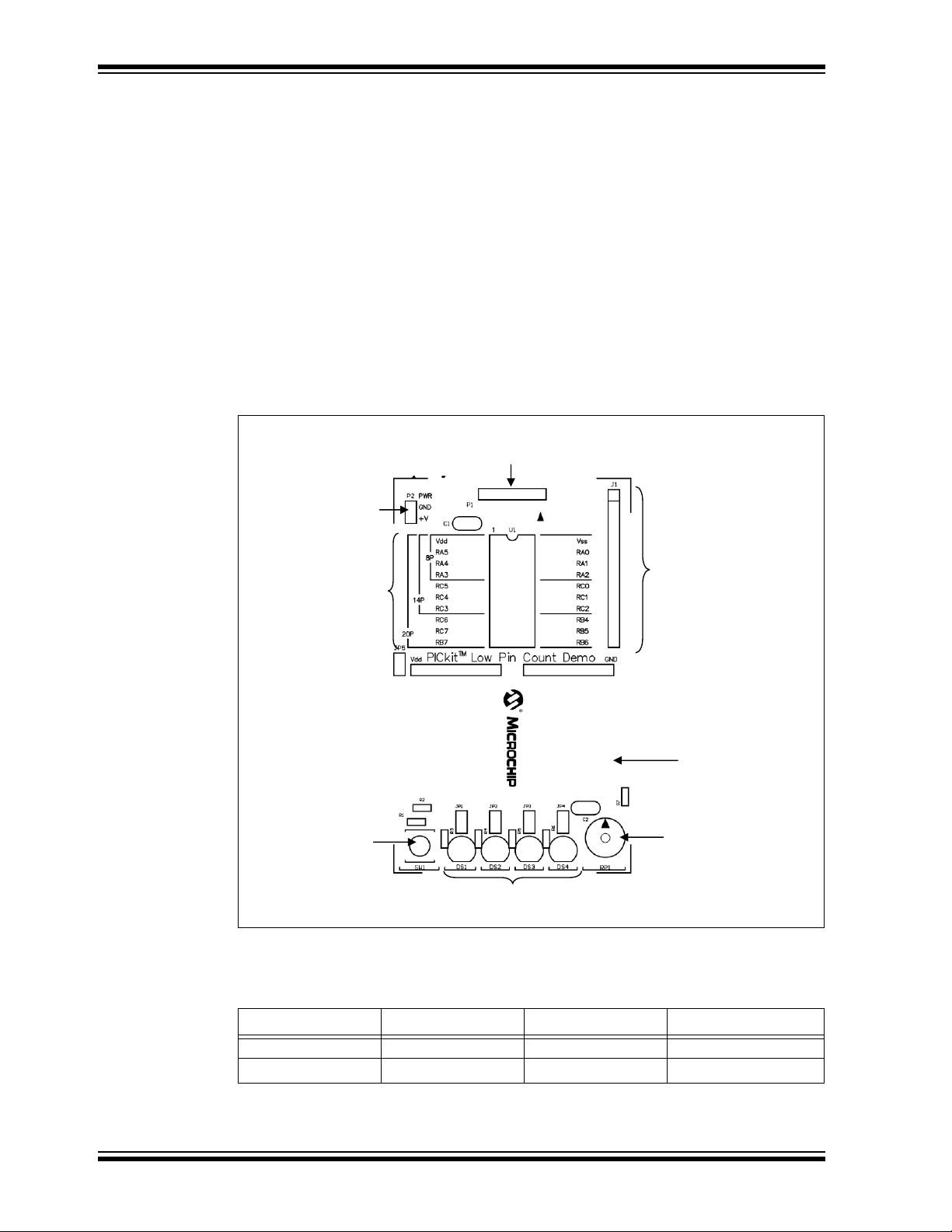
20-pin DIP
Socket
External Power
Push Button
ICSP™ Programming Header
14-pin Expansion Header
Generous Prototyping
Area
Potentiometer
LEDs
The software associated with the kit supports the PIC16F1829 and PIC18F14K22. The
software is intended to run on these two devices, although the software can be easily
ported to other devices.
1.5 THE LOW PIN COUNT BOARD
Support for 18-pin devices requires some board modifications. 14- and 20-pin PIC
devices will have full access to all of the human interface devices. If an 8-pin part is
used, then the LEDs will have to be bridged to the necessary pins on the PIC MCU.
The switch and potentiometer are already connected to pins that are supported by an
8-pin device. The board provides holes next to the LEDs that can be easily soldered to
in order to create any desired hardware changes.
The board is programmable by an In-Circuit Serial Programmer™ (ICSP™), such as a
PICkit™ programmer. The board should be supplied with 5V. Figure 1-1 shows the LPC
Demo Board.
FIGURE 1-1: DEMO BOARD HARDWARE LAYOUT
Ta bl e 1 -1 lists the components that are connected to the two PIC devices that come
with the board.
TABLE 1-1: PIN ASSIGNMENTS
Device LEDs <DS4:DS1> Switch – SW1 Potentiometer – RP1
PIC16F1829 <RC4:RC0> RA2 RA4
PIC18F14K22 <RC4:RC0> RA2 RA4
DS41628B-page 14 2012 Microchip Technology Inc.
Page 15

1.6 SOFTWARE OVERVIEW
This guide will assume that the reader has a basic knowledge of electronics. The
reader does not need to have any programming experience with a PIC MCU before
reading, although a basic knowledge of programming and what the difference between
a bit and byte will help.
The software is written in both assembly and ‘C’ in the MPLAB X and MPLAB 8 integrated design environment (IDE). The assembly version is more complex and requires
more lines of code, however it is closely tied to the PIC device’s hardware and the
reader will gain a much better understanding by doing these lessons in parallel with the
‘C’ routines. The ‘C’ programming language is a higher level language assembly, hence
it provides the reader with an easier to read flow of the program. Each lesson has both
versions and are functionally equivalent.
It is recommended that the lessons be followed sequentially, as presented, since most
of the lessons build up on one another. Each new program will introduce a new peripheral or concept. This guide is not intended to be read without following along in the
code.
The PIC18 and enhanced PIC16 programs will be presented side-by-side and their
differences and similarities explained.
1.7 RUNNING THE DEMONSTRATIONS
Overview
The board comes preprogrammed with a lesson. To use this program, either apply 5V
to the power header (P2), or connect a programmer to the programmer header (P1)
and apply 5V through the programmer in the IDE. The demo program will blink the four
red LEDs in succession. Press the push button (SW1), and the sequence will reverse.
Rotate the potentiometer (RP1), and the light sequence will blink at a different rate. This
demo program is developed through the first seven lessons in this guide.
2012 Microchip Technology Inc. DS41628B-page 15
Page 16

PICkit™ 3 Starter Kit User’s Guide
NOTES:
DS41628B-page 16 2012 Microchip Technology Inc.
Page 17
Chapter 2. PIC® MCU Architecture
Data Bus
8
14
Program
Bus
Instruction reg
Program Counter
8 Level Stack
(13-bit)
Direct Addr
7
12
Addr MUX
FSR reg
STATUS reg
MUX
ALU
Power-up
Timer
Oscillator
Start-up Timer
Power-on
Reset
Watchdog
Timer
Instruction
Decode &
Control
Timi ng
Generation
OSC1/CLKIN
OSC2/CLKOUT
V
DD
8
8
Brown-out
Reset
12
3
V
SS
Internal
Oscillator
Block
Configuration
Data Bus
8
14
Program
Bus
Instruction reg
Program Counter
8 Level Stack
(13-bit)
7
Addr MUX
FSR reg
STATUS reg
MUX
ALU
W Reg
Instruction
Decode &
Control
Timi ng
Generation
V
DD
8
8
3
V
SS
Internal
Oscillator
Block
Configuration
15
Data Bus
8
14
Program
Bus
Instruction Reg
Program Counter
16-Level Stack
(15-bit)
7
RAM Addr
Addr MUX
Indirect
Addr
FSR0 Reg
STATUS Reg
MUX
ALU
Instruction
Decode and
Control
Timi ng
Generation
V
DD
8
8
3
V
SS
Internal
Oscillator
Block
Configuration
Flash
Program
Memory
RAM
FSR regFSR reg
FSR1 Reg
15
15
MUX
15
Program Memory
Read (PMR)
12
FSR regFSR reg
BSR Reg
5
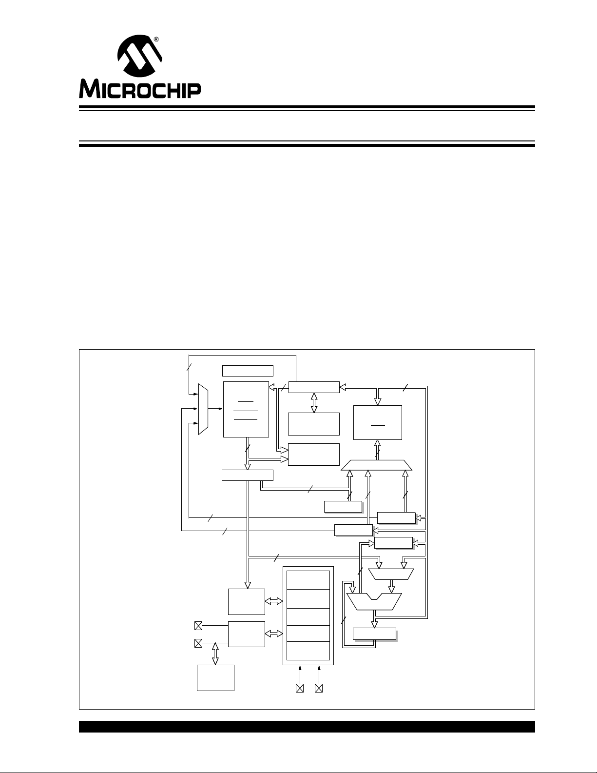
2.1 INTRODUCTION
This chapter describes the architecture of the enhanced mid-range PIC16F1829
(DS41440), as well as the PIC18 (DS41365).
2.2 CORE BASICS
Enhanced PIC16 and PIC18 devices use a modified Harvard architecture, meaning the
code memory and data memory are independent. This allows faster execution because
code instructions and data can be accessed simultaneously. The subsequent instruction is fetched while decoding and executing the current instruction. In Figure 2-1 and
Figure 2-3, the reader should notice the separate lines for data bus and program bus.
This guide will cover nearly all of the registers and modules as seen in the following
figures. The following block diagrams should be referenced while each lesson is being
performed in order to understand the interactions.
PICkit™ 3 STARTER KIT USER’S GUIDE
FIGURE 2-1: SIMPLIFIED ENHANCED MID-RANGE PIC
®
MCU BLOCK DIAGRAM
2012 Microchip Technology Inc. DS41628B-page 17
Page 18
PICkit™ 3 Starter Kit User’s Guide
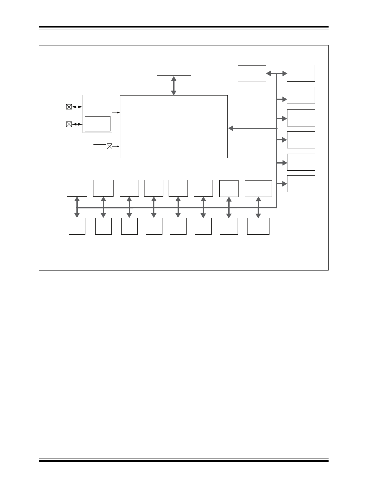
PORTA
EUSART
Comparators
MSSP
Timer2Timer1 Timer4Timer0
ECCP1
ADC
10-Bit
ECCP2 ECCP3 CCP4 CCP5
Timer6
PORTB
PORTC
PORTD
PORTE
LCD
SR
Latch
Note 1: See applicable chapters for more information on peripherals.
CPU
Program
Flash Memory
EEPROM
RAM
Timing
Generation
INTRC
Oscillator
MCLR
OSC1/CLKIN
OSC2/CLKOUT
Figure 2-1
FIGURE 2-2: SIMPLIFIED ENHANCED MID-RANGE PIC® MCU DATA BLOCK DIAGRAM
DS41628B-page 18 2012 Microchip Technology Inc.
Page 19
FIGURE 2-3: SIMPLIFIED PIC18 BLOCK DIAGRAM
Instruction
Decode and
Control
PORTA
PORTB
PORTC
RA1
RA0
Data Latch
Data Memory
Address Latch
Data Address<12>
12
Access
BSR
FSR0
FSR1
FSR2
inc/dec
logic
Address
4
12
4
PCH PCL
PCLATH
8
31-Level Stack
Program Counter
PRODLPRODH
8 x 8 Multiply
8
BITOP
8
8
ALU<8>
20
8
8
Table Pointer<21>
inc/dec logic
21
8
Data Bus<8>
Table Latch
8
IR
12
3
ROM Latch
PCLATU
PCU
Note 1: RA3 is only available when MCLR functionality is disabled.
2: OSC1/CLKIN and OSC2/CLKOUT are only available in select oscillator modes and when these pins are
not being used as digital I/O.
EUSARTComparator
MSSP
10-bit
ADC
Timer2Timer1 Timer3Time r0
ECCP1
BOR
Data
EEPROM
W
Instruction Bus <16>
STKPTR
Bank
8
State machine
control signals
Decode
8
8
Power-up
Timer
Oscillator
Start-up Timer
Power-on
Reset
Watchdog
Timer
OSC1
(2)
OSC2
(2)
VDD,
Internal
Oscillator
Fail-Safe
Clock Monitor
Precision
Reference
Band Gap
V
SS
MCLR
(1)
Block
LFINTOSC
Oscillator
16 MHz
Oscillator
Single-Supply
Programming
FVR
FVR
FVR
CV
REF
Address Latch
Program Memory
Data Latch
CV
REF
RA3
RA4
RA5
RB4
RB5
RB6
RB7
RC0
RC1
RC2
RC3
RC4
RC5
RC6
RC7
(512/768 bytes)
RA1
PIC® MCU Architecture
2012 Microchip Technology Inc. DS41628B-page 19
Page 20

PICkit™ 3 Starter Kit User’s Guide
T c lock cycle
1
F
OSC
-------------=
4 * T
4
FOSC
-------------
4
4 MHz
------------- ----
1 µs== =
BTFSS PORTA, RA0
2.3 DATA/PROGRAM BUS
The data bus is connected to the outside world via port pins, as well as all of the peripheral registers (timers, ADC, PWM). The program bus connects to the Flash memory
where the program is stored. This is where assembled code is programmed to.
2.4 ACCUMULATOR
There is only one accumulator – the working register (WREG). The accumulator handles all data bus related tasks, such as mathematical operations. The ALU only deals
with 8-bit sized data – hence the categorical names of 8/16/32-bit micros.
2.5 INSTRUCTIONS
Instructions tell what the PIC device should do, whether it is shifting a few bits or jumping to a new line in code. They form the very essence of each program in program
memory. All enhanced mid-range PIC devices have only 49 instructions. The PIC18
has 75 available instructions. Since there are very few instructions needed to learn, the
PIC device can be referred to as a “reduced instruction set computing”, or RISC,
processor.
Each instruction will be explained in detail as they are introduced in each lesson. For
now, the basis of what makes up each instruction will be explained.
One instruction cycle consists of four clock cycles. This means that if the PIC MCU is
running at 4 MHz, each instruction will take one microsecond, as seen in Equation 2-1.
EQUATION 2-1: INSTRUCTION TIME
All instructions are executed in a single instruction cycle, unless a conditional test is
true, or the program counter (PC) is changed. In these cases, the execution takes two
instruction cycles, with the additional instruction cycle executed as a NOP (do nothing),
see Example 2-1.
EXAMPLE 2-1:
This takes two instruction cycles only if pin RA0 is set (active-high), since the skip operation affects the PC.
The PIC18 has a larger word size than the enhanced PIC16 architecture. The PIC18
has a 16-bit wide word containing the operation code (opcode) and all required operands. The enhanced PIC16 has a 14-bit wide word. An opcode is interpreted by the
processor and is unique to each instruction.
The opcodes are broken into four formats:
1. Byte oriented
2. Bit oriented
3. Literal
4. Control
DS41628B-page 20 2012 Microchip Technology Inc.
Page 21

2.6 BYTE
ADDWF data,f
BSF PORTA,RA0
MOVLW ‘A’
PIC® MCU Architecture
All byte instructions on the enhanced PIC16 contain a 6-bit opcode, 7-bit file address,
and a destination bit. All PIC18 byte instructions contain a 6-bit opcode, 8-bit file
address, a destination bit, and a RAM access bit.The sum of all the bit field sizes confirms that the PIC16 enhanced core does indeed have a 14-bit wide word size for
instructions. Likewise, the same can be seen for the PIC18 for its 16-bit wide word
length.
The RAM access bit (a) on the PIC18 is set when the user wishes to use the Bank
Select Register (BSR) for manually selecting the bank. The PIC16 user will always
need to make sure that they are in the correct bank by using the ‘banksel’ directive.
This is explained in the first few lessons.
The destination bit (d) specifies whether the result will be stored in WREG or back in
the original file register. When ‘d’ is zero, the result is placed in the WREG resister.
Otherwise, the result is placed in the file register.
The file register (f) specifies which register to use. This can be a Special Function
Register (SFR) or General Purpose Register (GPR).
EXAMPLE 2-2:
2.7 BIT
2.8 LITERAL
This adds the contents of WREG and data, with the result being saved back to the file
register data.
The PIC18 can move data from one file register directly to another file register, circumventing the WREG. All file moves in the enhanced PIC16 architecture must go through
the WREG.
Bit instructions operate on a specific bit within a file register. These instructions may set
or clear a specific bit within a file register. They may also be used to test a specific bit
within a file register. All bit instructions on the enhanced PIC16 contain a 4-bit opcode,
7-bit file address, and a 3-bit bit address. All PIC18 byte instructions contain a 4-bit
opcode, 8-bit file address, 3-bit bit address and a RAM access bit.
EXAMPLE 2-3:
This sets pin RA0 in the PORTA register.
Literal operations contain the data operand within the instruction. Both architectures
use an 8-bit intermediate value. The rest of the bits are reserved for the opcode.
EXAMPLE 2-4:
This moves the ASCII value of ‘A’ (0x41) into WREG.
2012 Microchip Technology Inc. DS41628B-page 21
Page 22

PICkit™ 3 Starter Kit User’s Guide
2.9 CONTROL
Instructions that dictate what address the PC will select in program memory are called
control instructions. This would include call, goto, and branch. Each has a unique
word length. Please refer to the “Instruction Set Summary” chapter in any PIC
data sheet for more information.
device
DS41628B-page 22 2012 Microchip Technology Inc.
Page 23
PIC® MCU Architecture
Byte-oriented file register operations
13 8 7 6 0
d = 0 for destination W
OPCODE d f (FILE #)
d = 1 for destination f
f = 7-bit file register address
Bit-oriented file register operations
13 10 9 7 6 0
OPCODE b (BIT #) f (FILE #)
b = 3-bit bit address
f = 7-bit file register address
Literal and control operations
13 8 7 0
OPCODE k (literal)
k = 8-bit immediate value
13 11 10 0
OPCODE k (literal)
k = 11-bit immediate value
General
CALL and GOTO instructions only
MOVLP instruction only
13 5 4 0
OPCODE k (literal)
k = 5-bit immediate value
MOVLB instruction only
13 9 8 0
OPCODE k (literal)
k = 9-bit immediate value
BRA instruction only
FSR Offset instructions
13 7 6 5 0
OPCODE n k (literal)
n = appropriate FSR
FSR Increment instructions
13 7 6 0
OPCODE k (literal)
k = 7-bit immediate value
13 3 2 1 0
OPCODE n m (mode)
n = appropriate FSR
m = 2-bit mode value
k = 6-bit immediate value
13 0
OPCODE
OPCODE only
ADDWF MYREG, W
BSF MYREG, BIT
MOVLW 0x45
CALL LABEL
MOVLP 15
MOVLB 3
BRA LABEL
ADDFSR FSR1, 3
MOVIW ++FSR0
Example Instruction
FIGURE 2-4: ENHANCED PIC16 GENERAL FORMAT FOR INSTRUCTIONS
2012 Microchip Technology Inc. DS41628B-page 23
Page 24

PICkit™ 3 Starter Kit User’s Guide
Byte-oriented file register operations
15 10 9 8 7 0
d = 0 for result destination to be WREG register
OPCODE d a f (FILE #)
d = 1 for result destination to be file register (f)
a = 0 to force Access Bank
Bit-oriented file register operations
15 12 11 9 8 7 0
OPCODE b (BIT #) a f (FILE #)
b = 3-bit position of bit in file register (f)
Literal operations
15 8 7 0
OPCODE k (literal)
k = 8-bit immediate value
Byte to Byte move operations (2-word)
15 12 11 0
OPCODE f (Source FILE #)
CALL, GOTO and Branch operations
15 8 7 0
OPCODE n<7:0> (literal)
n = 20-bit immediate value
a = 1 for BSR to select bank
f = 8-bit file register address
a = 0 to force Access Bank
a = 1 for BSR to select bank
f = 8-bit file register address
15 12 11 0
1111 n<19:8> (literal)
15 12 11 0
1111 f (Destination FILE #)
f = 12-bit file register address
Control operations
Example Instruction
ADDWF MYREG, W, B
MOVFF MYREG1, MYREG2
BSF MYREG, bit, B
MOVLW 7Fh
GOTO Label
15 8 7 0
OPCODE n<7:0> (literal)
15 12 11 0
1111 n<19:8> (literal)
CALL MYFUNC
15 11 10 0
OPCODE n<10:0> (literal)
S = Fast bit
BRA MYFUNC
15 8 7 0
OPCODE n<7:0> (literal)
BC MYFUNC
S
FIGURE 2-5: PIC18 GENERAL FORMAT FOR INSTRUCTIONS
There are some subtle differences between the block diagrams in Figure 2-1 and
Figure 2-3. This document will point out a few of the important ones.
DS41628B-page 24 2012 Microchip Technology Inc.
Page 25

2.10 STACK LEVEL
The PIC18 has a deeper stack level of 31, whereas the enhanced core has 16. A
deeper stack allows the PIC device to make more calls in the software before returning
to the original address where the first call was made.
A call or goto modifies the program counter to point to a different place in code. Without these, the code would execute from the top to the bottom. The lessons will show
the significance of this.
The call stack is used to save the return address before going to a new position in
program memory.
As a frame of reference, some of the baseline parts (PIC10/12) devices have a call
stack that is only two levels deep. It is quite a challenge to create modular code with a
limited stack depth.
2.11 MEMORY ORGANIZATION
There are three sections of memory in the PIC16 enhanced mid-range and PIC18
devices:
1. Program Memory
2. Data RAM
3. Data EEPROM
PIC® MCU Architecture
2.12 PROGRAM MEMORY
There are five sections of program memory:
1. Flash Program Memory
2. Configuration Words
3. Device ID
4. Revision ID
5. User ID
2.12.1 Flash Program Memory
All enhanced mid-range and PIC18 devices use Flash memory for programming. Flash
allows the PIC device to be erased and written to hundreds of thousands of times.
2.12.2 Configuration Words
There are several Configuration Word bits, or fuses, that allow different configurations
at run-time. Oscillator selections, memory protection, low-voltage detection, etc., are
some examples of configuration options. Each device has different configuration
options. Enhanced mid-range Configuration bits are read-only during code execution.
PIC18 can read all and write most Configuration bits during code execution. The
Configuration bits are programmed in a special way, as seen in the lesson source files.
2.12.3 Device ID
The Device ID contains the read-only manufacture’s ID for the PIC MCU. The
PIC16F1829 ID is stored in DEVICEID and the PIC18F14K22 is stored in DEVID1 and
DEVID2.
2012 Microchip Technology Inc. DS41628B-page 25
Page 26
PICkit™ 3 Starter Kit User’s Guide
PC<14:0>
15
0000h
0004H
Stack Level 0
Stack Level 15
Reset Vecto r
Interrupt Vector
Stack Level 1
0005h
On-chip
Program
Memory
Page 0
07FFh
Rollover to Page 0
0800h
0FFFh
1000h
7FFFh
Page 1
Rollover to Page 3
Page 2
Page 3
17FFh
1800h
1FFFh
2000h
CALL
, CALLW
RETURN, RETLW
Interrupt, RETFIE
2.12.4 Revision ID
There are five bits in each PIC MCU that indicate the silicon revision of the PIC device.
These bits are read-only and found in the DEVID register. There are usually multiple
revisions of silicon for each PIC device. The errata document, which points out any
errors and their temporary work-arounds, should be read alongside the data sheet.
The PIC18 has a program bus that is 21 bits wide, whereas the enhanced core is only
15 bits wide. A larger program bus infers that the program memory is larger, since it
allows the core to locate a higher address value. The enhanced core program counter
is capable of addressing 32K x 14 program memory space as seen in Figure 2-6.
FIGURE 2-6: ENHANCED MID-RANGE PROGRAM MEMORY MAP AND
CALL STACK
PIC18 devices are capable of addressing a 2-Mbyte program memory space, as seen
in Figure 2-7. PIC18 devices also have two interrupt vectors, whereas the enhanced
PIC devices only have one. A stark difference is that the PIC18 has no concept of
pages, whereas the enhanced core has its program memory split into different pages.
DS41628B-page 26 2012 Microchip Technology Inc.
Page 27
PIC® MCU Architecture
PC<20:0>
Stack Level 1
Stack Level 31
Reset Vector
Low Priority Interrupt Vector
CALL,RCALL,RETURN
RETFIE,RETLW
21
0000h
0018h
High Priority Interrupt Vector
0008h
User Memory Space
1FFFFFh
4000h
3FFFh
200000h
On-Chip
Program Memory
Read ‘0’
1FFFh
2000h
On-Chip
Program Memory
Read ‘0’
PIC18(L)F14K22
PIC18(L)F13K22
Changing pages is necessary in the enhanced core when changing execution from one
page to another. None of the lessons for the enhanced PIC16 occupy more than one
page and, therefore, page changes are not necessary. If the code does overflow into
another page, the assembler will give a warning, indicating that a pagesel may be
required.
FIGURE 2-7: PIC18 PROGRAM MEMORY MAP AND CALL STACK
2.13 DATA MEMORY
2.12.5 User ID
These four memory locations are designated as ID locations where the programmer
can store checksum or other code identification numbers. These are readable and
writable during normal execution.
The data memory layout of the two device families is perhaps the most significant. Data
memory on both families can be split into four types:
1. Core Registers
2. Special Function Registers
3. General Purpose RAM
4. Common RAM
2012 Microchip Technology Inc. DS41628B-page 27
Page 28

PICkit™ 3 Starter Kit User’s Guide
2.13.1 Core Registers
The core registers contain the registers that directly affect the basic operation of the
PIC device, repeated at the top of every data memory bank. Here are three examples
of the 12 core registers:
1. STATUS
2. WREG
3. INTCON
The STATUS register contains the arithmetic status of the ALU. The WREG register is
used to move bits in and out of registers. The INTCON register contains the various
enable and flag bits that would cause the PIC MCU to jump to the Interrupt Vector.
2.13.2 Special Function Registers
The Special Function Registers provide access to the peripheral functions in the
device. The Special Function Registers occupy 20 bytes immediately after the core registers of every data memory bank (addresses x0Ch/x8Ch through x1Fh/x9Fh) on the
enhanced mid-range core. The PIC18 enhanced core has all of its SFRs in Access
RAM, which is discussed in Section 2.14 “Banks”.
2.13.3 General Purpose RAM
2.14 BANKS
GPRs are used for data storage and scratchpad operations in the user’s application.
Think of this as RAM that can be used for your program, but the correct bank must be
selected before using. For the enhanced mid-range PIC devices, there are up to 80
bytes of GPR that follow immediately after the SFR space in each data memory bank.
2.13.4 Common RAM
There are 16 bytes of common RAM accessible from all banks in the enhanced core.
The PIC18 architecture has something similar called Access RAM, which contains up
to 96 bytes.
The PIC18F14K22 data memory is divided into 16 banks that contain 256 bytes each.
The PIC16F1829 data memory is partitioned in 32 memory banks with 128 bytes in
each bank. For the PIC16 enhanced mid-range, each bank consists of:
1. 12 core registers
2. 20 Special Function Registers (SFR)
3. Up to 80 bytes of General Purpose RAM (GPR)
4. 16 bytes of shared RAM (accessible by any bank)
Figure 2-8 shows the above information on the enhanced PIC16.
DS41628B-page 28 2012 Microchip Technology Inc.
Page 29

PIC® MCU Architecture
0Bh
0Ch
1Fh
20h
6Fh
70h
7Fh
00h
Common RAM
(16 bytes)
General Purpose RAM
(80 bytes maximum)
Core Registers
(12 bytes)
Special Function Registers
(20 bytes maximum)
Memory Region
7-bit Bank Offset
FIGURE 2-8: ENHANCED MID-RANGE BANKED MEMORY PARTITIONING
Addresses 70h-7Fh are shared by all of the banks. This is useful for storing a few bytes
of RAM without the need to switch banks each time the byte is used. Figure 2-9 shows
the first eight banks on the PIC16F1829. Notice how the top 12 core registers are
accessible from every bank, as are the 16 bytes of common RAM.
2012 Microchip Technology Inc. DS41628B-page 29
Page 30
DS41628B-page 30 2012 Microchip Technology Inc.
FIGURE 2-9: PIC16F1829 MEMORY MAP – THE CORRECT BANK MUST BE SELECTED BEFORE WRITING/READING FROM A
PICkit™ 3 Starter Kit User’s Guide
REGISTER
BANK 0 BANK 1 BANK 2 BANK 3 BANK 4 BANK 5 BANK 6 BANK 7
000h INDF0 080h INDF0 100h INDF0 180h INDF0 200h INDF0 280h INDF0 300h INDF0 380h INDF0
001h INDF1 081h INDF1 101h INDF1 181h INDF1 201h INDF1 281h INDF1 301h INDF1 381h INDF1
002h PCL 082h PCL 102h PCL 182h PCL 202h PCL 282h PCL 302h PCL 382h PCL
003h STATUS 083h STATUS 103h STATUS 183h STATUS 203h STATUS 283h STATUS 303h STATUS 383h STATUS
004h FSR0L 084h FSR0L 104h FSR0L 184h FSR0L 204h FSR0L 284h FSR0L 304h FSR0L 384h FSR0L
005h FSR0H 085h FSR0H 105h FSR0H 185h FSR0H 205h FSR0H 285h FSR0H 305h FSR0H 385h FSR0H
006h FSR1L 086h FSR1L 106h FSR1L 186h FSR1L 206h FSR1L 286h FSR1L 306h FSR1L 386h FSR1L
007h FSR1H 087h FSR1H 107h FSR1H 187h FSR1H 207h FSR1H 287h FSR1H 307h FSR1H 387h FSR1H
008h BSR 088h BSR 108h BSR 188h BSR 208h BSR 288h BSR 308h BSR 388h BSR
009h WREG 089h WREG 109h WREG 189h WREG 209h WREG 289h WREG 309h WREG 389h WREG
00Ah PCLATH 08Ah PCLATH 10Ah PCLATH 18Ah PCLATH 20Ah PCLATH 28Ah PCLATH 30Ah PCLATH 38Ah PCLATH
00Bh INTCON 08Bh INTCON 10Bh INTCON 18Bh INTCON 20Bh INTCON 28Bh INTCON 30Bh INTCON 38Bh INTCON
00Ch PORTA 08Ch TRISA 10Ch LATA 18Ch ANSELA 20Ch WPUA 28Ch — 30Ch — 38Ch INLVLA
00Dh PORTB
00Eh PORTC 08Eh TRISC 10Eh LATC 18Eh ANSELC 20Eh WPUC 28Eh —30Eh—38EhINLVLC
00Fh
010h
011h PIR1 091h PIE1 111h CM1CON0 191h EEADRL 211h
012h PIR2 092h PIE2 112h CM1CON1 192h EEADRH 212h
013h
014h
015h TMR0 095h OPTION_REG 115h CMOUT 195h EECON1 215h
016h
017h
018h
019h
01Ah
01Bh
01Ch
01Dh
01Eh CPSCON0 09Eh ADCON1 11Eh APFCON1 19Eh TXSTA 21Eh
01Fh CPSCON1 09Fh
020h
06Fh 0EFh 16Fh 1EFh 26Fh 2EFh
070h 0F0h
07Fh 0FFh 17Fh 1FFh 27Fh 2FFh 37Fh 3FFh
Legend: = Unimplemented data memory locations, read as ‘0’.
Note 1: Available only on PIC16(L)F1829.
(1)
08Dh TRISB
(1)
10Dh LATB
(1)
18Dh ANSELB
(1)
20Dh WPUB
(1)
28Dh — 30Dh — 38Dh INLVLB
—08Fh—10Fh—18Fh—20Fh—28Fh—30Fh—38Fh—
—090h—110h—190h—210h—290h— 310h — 390h —
—093h— 113h CM2CON0 193h EEDATL 213h
—094h— 114h CM2CON1 194h EEDATH 214h
TMR1L 096h PCON 116h BORCON 196h EECON2 216h
TMR1H 097h WDTCON 117h FVRCON 197h
T1CON 098h OSCTUNE 118h DACCON0 198h
—217h
—218h
T1GCON 099h OSCCON 119h DACCON1 199h RCREG 219h
TMR2 09Ah OSCSTAT 11Ah SRCON0 19Ah TXREG 21Ah
PR2 09Bh ADRESL 11Bh SRCON1 19Bh SPBRGL 21Bh
T2CON 09Ch ADRESH 11Ch
— 19Ch SPBRGH 21Ch
— 09Dh ADCON0 11Dh APFCON0 19Dh RCSTA 21Dh
—11Fh— 19Fh BAUDCON 21Fh
General
Purpose
0A0h
General
Purpose
Register
80 Bytes
120h
General
Purpose
Register
80 Bytes
1A0h
General
Purpose
Register
80 Bytes
220h
Register
96 Bytes
Accesses
70h – 7Fh
170h
Accesses
70h – 7Fh
1F0h
Accesses
270h
70h – 7Fh
SSP1BUF
SSP1ADD
SSP1MSK
SSP1STAT
SSP1CON
SSP1CON2
SSP1CON3
—
SSP2BUF
SSP2ADD
SSP2MSK
SSP2STAT
SSP2CON
SSP2CON2
SSP2CON3
General
Purpose
Register
80 Bytes
Accesses
70h – 7Fh
291h CCPR1L 311h
292h CCPR1H 312h
293h CCP1CON 313h
294h PWM1CON 314h
295h CCP1AS 315h
296h PSTR1CON 316h
297h — 317h
298h
(1)
299h
(1)
29Ah
(1)
29Bh
(1)
29Ch
(1)
29Dh
(1)
29Eh
(1)
29Fh
CCPR2L
CCPR2H
CCP2CON
PWM2CON
CCP2AS
PSTR2CON
CCPTMRS
—
2A0h
General
Purpose
Register
80 Bytes
2F0h
Accesses
70h – 7Fh
318h
319h
31Ah
31Bh
31Ch
31Dh
31Eh
31Fh
320h
36Fh
370h
CCPR3L
CCPR3H
CCP3CON
—
—
—
—
CCPR4L
CCPR4H
CCP4CON
—
—
—
—
—
General
Purpose
Register
80 Bytes
Accesses
70h – 7Fh
391h IOCAP
392h IOCAN
393h
394h IOCBP
395h IOCBN
396h IOCBF
397h
398h
399h —
39Ah CLKRCON
39Bh
39Ch MDCON
39Dh
39Eh
39Fh
3A0h
3EFh
3F0h
IOCAF
(1)
(1)
(1)
—
—
—
MDSRC
MDCARL
MDCARH
General
Purpose
Register
80 Bytes
Accesses
70h – 7Fh
(1)
Page 31

PIC® MCU Architecture
When using the PIC16F1829 in assembly, the reader will be constantly referring back
to Figure 2-9 to make sure that the right bank is selected before writing to an SFR.
For PIC18 devices, the banking situation was streamlined so that the user does not
have to switch banks when using the access SFRs. The data memory is configured
with an Access Bank, which allows users to access a mapped block of memory without
specifying a Bank Select Register (BSR). The Access Bank consists of the first 96
bytes of memory in Bank 0 and the last 160 bytes of memory in Bank Block 15. This
lower half is known as the “Access RAM” and is composed of GPRs. The upper half is
where the device’s SFRs are mapped (Bank 15). When going through the assembly
lessons, the reader will notice the absence of bank switching. Figure 2-10 and
Figure 2-11 show this improved mapping scheme.
2012 Microchip Technology Inc. DS41628B-page 31
Page 32

PICkit™ 3 Starter Kit User’s Guide
Bank 0
Bank 1
Bank 14
Bank 15
Data Memory Map
BSR<3:0>
= 0000
= 0001
= 1111
060h
05Fh
F60h
FFFh
00h
5Fh
60h
FFh
Access Bank
When ‘a’ = 0:
The BSR is ignored and the
Access Bank is used.
The first 96 bytes are
general purpose RAM
(from Bank 0).
The second 160 bytes are
Special Function Registers
(from Bank 15).
When ‘a’ = 1:
The BSR specifies the bank
used by the instruction.
F5Fh
F00h
EFFh
1FFh
100h
0FFh
000h
Access RAM
FFh
00h
FFh
00h
FFh
00h
GPR
SFR
Access RAM High
Access RAM Low
Bank 2
= 0110
= 0010
(SFRs)
2FFh
200h
3FFh
300h
4FFh
400h
5FFh
500h
6FFh
600h
7FFh
700h
8FFh
800h
9FFh
900h
AFFh
A00h
BFFh
B00h
CFFh
C00h
DFFh
D00h
E00h
Bank 3
Bank 4
Bank 5
Bank 6
Bank 7
Bank 8
Bank 9
Bank 10
Bank 11
Bank 12
Bank 13
FFh
00h
FFh
00h
FFh
00h
FFh
00h
FFh
00h
FFh
00h
FFh
00h
FFh
00h
FFh
00h
FFh
00h
FFh
00h
FFh
00h
FFh
00h
= 0011
= 0100
= 0101
= 0111
= 1000
= 1001
= 1010
= 1011
= 1100
= 1101
= 1110
Unused
Read 00h
Unused
F53h
SFR
(1)
Note 1: SFRs occupying F53h to F5Fh address space are not in the virtual bank.
FIGURE 2-10: PIC18F14K22 DATA MEMORY MAP
DS41628B-page 32 2012 Microchip Technology Inc.
Page 33

PIC® MCU Architecture
FIGURE 2-11: PIC18F14K22 SPECIAL FUNCTION REGISTER MAP – ALL OF THESE ARE IN
BANK 15 WHICH IS INCLUDED IN THE “ACCESS RAM”
Address Name Address Name Address Name Address Name Address Name
FFFh TOSU FD7h TMR0H FAFh SPBRG F87h
FFEh TOSH FD6h TMR0L FAEh RCREG F86h —
FFDh TOSL FD5h T0CON FADh TXREG F85h —
FFCh STKPTR FD4h —
(2)
FACh TXSTA F84h —
FFBh PCLATU FD3h OSCCON FABh RCSTA F83h —
FFAh PCLATH FD2h OSCCON2 FAAh —
(2)
F82h PORTC F5Ah —
(2)
—
(2)
(2)
(2)
(2)
F5Fh —
F5Eh —
F5Dh —
F5Ch —
F5Bh —
FF9h PCL FD1h WDTCON FA9h EEADR F81h PORTB F59h —
FF8h TBLPTRU FD0h RCON FA8h EEDATA F80h PORTA F58h —
FF7h TBLPTRH FCFh TMR1H FA7h EECON2
(1)
F7Fh ANSELH F57h —
FF6h TBLPTRL FCEh TMR1L FA6h EECON1 F7Eh ANSEL F56h —
FF5h TABLAT FCDh T1CON FA5h —
FF4h PRODH FCCh TMR2 FA4h —
FF3h PRODL FCBh PR2 FA3h —
(2)
(2)
(2)
F7Dh —
F7Ch —
F7Bh —
(2)
(2)
(2)
F55h —
F54h —
F53h —
FF2h INTCON FCAh T2CON FA2h IPR2 F7Ah IOCB
FF1h INTCON2 FC9h SSPBUF FA1h PIR2 F79h IOCA
FF0h INTCON3 FC8h SSPADD FA0h PIE2 F78h WPUB
(1)
FEFh INDF0
FEEh POSTINC0
FEDh POSTDEC0
FECh PREINC0
FEBh PLUSW0
FEAh FSR0H FC2h ADCON0 F9Ah —
FE9h FSR0L FC1h ADCON1 F99h —
FE8h WREG FC0h ADCON2 F98h —
FE7h INDF1
FE6h POSTINC1
FE5h POSTDEC1
FE4h PREINC1
FE3h PLUSW1
FE2h FSR1H FBAh VREFCON0 F92h TRISA F6Ah
FE1h FSR1L FB9h PSTRCON F91h —
FE0h BSR FB8h BAUDCON F90h
FDFh INDF2
FDEh POSTINC2
FDDh POSTDEC2
FDCh PREINC2
FDBh PLUSW2
FDAh FSR2H FB2h TMR3L F8Ah LATB F62h —
FD9h FSR2L FB1h T3CON F89h LATA F61h —
FD8h STATUS FB0h SPBRGH F88h —
FC7h SSPSTAT F9Fh IPR1 F77h WPUA
(1)
(1)
(1)
(1)
(1)
(1)
(1)
(1)
(1)
(1)
FB7h PWM1CON F8Fh —
(1)
(1)
(1)
(1)
FC6h SSPCON1 F9Eh PIR1 F76h SLRCON
FC5h SSPCON2 F9Dh PIE1 F75h —
FC4h ADRESH F9Ch —
(2)
F74h —
FC3h ADRESL F9Bh OSCTUNE F73h —
FBFh CCPR1H F97h —
FBEh CCPR1L F96h —
FBDh CCP1CON F95h —
(2)
(2)
(2)
(2)
(2)
(2)
F72h —
F71h —
F70h —
F6Fh SSPMASK
F6Eh —
F6Dh CM1CON0
FBCh VREFCON2 F94h TRISC F6Ch CM2CON1
FBBh VREFCON1 F93h TRISB F6Bh CM2CON0
FB6h ECCP1AS F8Eh —
FB5h —
FB4h —
(2)
(2)
F8Dh —
F8Ch —
(2)
(2)
—
(2)
(2)
(2)
(2)
F69h SRCON1
F68h SRCON0
F67h —
F66h —
F65h —
F64h —
FB3h TMR3H F8Bh LATC F63h —
(2)
F60h —
(2)
(2)
(2)
(2)
(2)
(2)
(2)
(2)
—
(2)
(2)
(2)
(2)
(2)
(2)
(2)
(2)
Legend: = Unimplemented data memory locations, read as ‘0’,
Note 1: This is not a physical register.
2: Unimplemented registers are read as ‘0’.
All of the SFRs in Figure 2-9 are in Bank 15 and do not require banking since this bank
is covered by the Access Bank. Switching banks in the enhanced mid-range core
requires two instructions, so this could potentially save a great number of instructions
in the overall program.
(2)
(2)
(2)
(2)
(2)
(2)
(2)
(2)
(2)
(2)
(2)
(2)
(2)
2012 Microchip Technology Inc. DS41628B-page 33
Page 34

PICkit™ 3 Starter Kit User’s Guide
code.asm
code.hex Programmer
MPASM™
assembler
MCU
2.15 DATA EEPROM MEMORY
The data EEPROM is a nonvolatile memory array, separate from both the data RAM,
and program memory, which is used for long-term storage of program data. The
EEPROM is not directly mapped in either the register file or program memory space,
but is indirectly addressed through special SFRs. The EEPROM is readable and
writable during normal operation.
The PIC16F1829 and PIC18F14K22 have 256 bytes of EEPROM on board.
The EEPROM is rated for high erase/write cycle endurance. A byte write automatically
erases the location and writes the new data. Please see Section 3.14 “Lesson 13:
EEPROM” for more information.
2.16 PROGRAMMING BASICS
This section will briefly discuss essential assembler and ‘C’ basics. There are better
suited tutorials on ‘C’ programming on the web if the user wishes to learn more.
This guide uses the XC8 compiler v.1.00 for both the PIC16F1829 and PIC18F14K22.
Later versions of the compiler will also work. Looking at the XC8 user’s guide would be
a very good start. One of the great benefits of using ‘C’ is that it is very portable and will
build in most compilers with no problem.
The assembly is not compiled, but rather assembled by a utility called MPASM. This
guide uses MPASM assembler v5.43, which is a universal assembler for all PIC1X
devices.
A key advantage of using a high-level language (such as C) is that the programmer
does not need to understand the architecture of the microprocessor being used. Knowledge of the architecture is left to the compiler which will take the ‘C’ and compile it into
assembly. When using assembly, the programmer must use the PIC device’s instruction set and understand the memory map. A positive benefit of assembly is not only the
knowledge gained, but also the code size will be considerably smaller.
2.16.1 MPASM™ Assembler Operation
All of the lessons written in are absolute code. This means that everything that the
assembler needs is contained in the source files. This process is shown below.
FIGURE 2-12: MPASM ASSEMBLER OPERATION
When a source file is assembled in this manner, all variables and routines used in the
source file must be defined within that source file, or in files that have been explicitly
included by that source file. If assembly proceeds without errors, a hex file will be generated that contains the executable machine code for the targeted PIC device. This file
can then be used by the debugger to test code execution, and by a device programmer
to program the microcontroller.
2.16.2 XC8 Operation
The compiler does all of the translation involved, which is needed to take the high-level
code down to a level in which the PIC device understands. Figure 2-13 explains how
this is done.
DS41628B-page 34 2012 Microchip Technology Inc.
Page 35

FIGURE 2-13: XC8 OPERATION
PIC® MCU Architecture
Notice how the output is the same for both the compiler/assembler – a hex file. The
assembly that the compiler generates can be seen in the disassembly window inside
of the MPLAB
FIGURE 2-14: DISASSEMBLY FIGURE
Figure 2-14 shown above shows part of the disassembly of lesson 5. The ‘C’, which is
indented, is easier to understand and write. The assembly underneath it contains twice
as much code, and includes the PIC MCU specific instructions to achieve the desired
result of the ‘C’ above it.
®
IDE.
2012 Microchip Technology Inc. DS41628B-page 35
Page 36

PICkit™ 3 Starter Kit User’s Guide
cblock [address]
Variable
endc
2.16.3 Numbers in the Assembler
Unless otherwise specified, the assembler assumes any numeric constants in the
program are hexadecimal (base 16). Binary (base 2), octal (base 8), decimal (base 10),
and ASCII coding are also supported.
TABLE 2-1: NUMBERS IN THE ASSEMBLER
Radix Format Example
Hexadecimal # or 0x# or H’#’ 12 or 0x12 or H’12’
Decimal .# or D’#’Octal or O’#’ .12 or D’12’Octal or O’12’
Binary B’#’ B’00010010’
ASCII A’#’ or ‘#’ A’c’ or ‘c’
2.16.4 Numbers in the XC8 Compiler
Unless otherwise specified, the compiler assumes any numeric constants in the
program are decimal (base 10).
TABLE 2-2: NUMBERS IN THE COMPILER
Radix Format Example
Hexadecimal 0x# 0x12
Decimal # 12
Binary 0b# 0b00010010
ASCII ‘#’ ‘c’
2.17 MPASM ASSEMBLER DIRECTIVES
Directives are assembler commands that appear in the source code, but are not usually
translated directly into opcodes. They are used to control the assembler: its input,
output, and data allocation.
Many of the assembler directives have alternate names and formats. These may exist
to provide backward compatibility with previous assemblers from Microchip, and to be
compatible with individual programming practices.
All of the directives for the MPASM assembler can be found inside the IDE under
Help->Help
2.17.1 Banksel
banksel label
This directive is an instruction to the assembler and linker to generate bank selecting
code to set the bank to the bank containing the designated label. The programmer
should always use this directive instead of setting the BSR directly, to avoid the possibility of human error.
2.17.2 cblock
EXAMPLE 2-5:
Contents
DS41628B-page 36 2012 Microchip Technology Inc.
This is used to define a block of variables starting at address address.
Page 37

EXAMPLE 2-6:
“MESSAGE 302 – Operand Not in Bank 0, check to ensure bank bits are correct”
include “include_file”
#include <include_file>
PIC® MCU Architecture
2.17.3 Org (addr)
Org tells the assembler where to start generating code at addr. Normally, the lessons
would start code at address 0x0000.
2.17.4 End
End tells the assembler to stop assembling. There must be one at the end of the
program. It does not necessarily have to be at the end of the file, but nothing after the
end statement will be assembled.
2.17.5 Errorlevel
This is used to suppress warnings that the assembler may give. It is vital that the
programmer understand the message before hiding them from the output window.
2.17.6 #include
EXAMPLE 2-7:
The specified file is read in as source code. The effect is the same as if the entire text
of the included file were inserted into the file at the location of the include statement.
The angled brackets (< >) indicate that the file can be found in the library folder of the
assembler. Double quotes ( “ “) indicate that the include file is in the current working
directory. The exact locations can be changed in the IDE.
2012 Microchip Technology Inc. DS41628B-page 37
Page 38

PICkit™ 3 Starter Kit User’s Guide
NOTES:
DS41628B-page 38 2012 Microchip Technology Inc.
Page 39

PICkit™ 3 STARTER KIT USER’S GUIDE
Chapter 3. Lessons
All of the following 13 lessons will include important code snippets, as well as new registers and instructions for each PIC MCU. Each lesson introduces either a new peripheral or feature. There may be slight differences between the PIC16 and PIC18 in each
lesson, but the differences are pointed out and explained. The enhanced PIC16 is
explained first, followed by the PIC18. There are sometimes minimal differences
between the two and, when none exist, a statement of “none” will appear in the PIC18
section(s).
Subsequent lessons inherit these differences, however they are explained only in their
first appearance. This is why it will be vital that the lessons are done in sequence.
These differences are mostly in the assembly, not in the ‘C’ programs due to the nature
of the language. It is strongly recommended that the assembly be done alongside the
‘C’ version for each lesson.
The lessons follow this folder structure:
1. <architecture>
a. <language>
i. <lesson>
1. <lesson>.X (MPLABX project)
2. Mplab8 (MPLAB 8.x project)
3. <lesson> . <language> (source file)
For example:
2. PIC16
a. Assy
i. 01 Hello World
1. Hello_world.X (MPLABX project)
2. Mplab8 (MPLAB 8.x project)
3. Hello_world.asm
b. C
i. 01 Hello World
1. Hello_world.X (MPLABX project)
2. Mplab8 (MPLAB 8.x project)
3. Hello_world.c
A single source file is shared between both projects, meaning that any changes to the
file while using MPLAB
aged that the new IDE, MPLAB
nothing else in the project folders.
Please see the getting started videos that are linked to on the Start Page inside of the
MPLAB X IDE. Refer to the MPLAB
(http://ww1.microchip.com/downloads/en/DeviceDoc/51281d.pdf
guide for MPLAB 8.XX.
®
X will be reflected in the MPLAB® 8 project as well. It is encour-
X, be used. Only the source file should be edited and
®
IDE Quick Start Guide (DS51281)
) as a getting started
2012 Microchip Technology Inc. DS41628B-page 39
Page 40

DS41628B-page 40 2012 Microchip Technology Inc.
PICkit™ 3 Starter Kit User’s Guide
3.1 LESSONS
# Lesson New Modules New Concepts New Registers New Instructions
1 Hello World ALU Latch Port Basics of PIC MCU
programming
2 Blink 1. GPR
2. SRF
3. ACCESS RAM
4. Oscillator
3 Rotate Bit Check STATUS BTFSC LSRF RRCF
4 Analog-to-Digital ADC Bit shift ANSEL ADCON0/1/2 SWAPF
5 Variable Speed
Rotate
6 Debounce Preprocessor Macros
7 Reversible
Variable Speed
Rotate
8Pulse-Width
Modulation
9 Timer0 Timer0 Timers OPTION_REG T0CON
10Interrupts and
Pull-ups
11Indirect
Addressing
12Look-up Table Program Memory Read 1. Memory
13EEPROM Nonvolatile Memory Low Power EECON2 SLEEP
1. Interrupt Vector (High/Low)
2. Weak pull-up
Hardware Stack Functions CALL RETURN XORWF
ECCP 1. PWM resolution
Virtual registers 1. Pointers INDFx FSRx INCF
1. Delay
2. I/O
3. Banking
Modular Code RLNCF
2. PWM frequency
3. Modulation
1. Usefulness of
interrupts
conservation
2. Self Read
3. State Machine
TRISC PORTC LATC BSF BCF CLRF
OSCCON MOVLW DECFSZ GOTO
MOVWF BRA BTG
TSTFSZ RCALL
CCPxCON PRx TxCON ANDLW
CCPTMRS CCPRxL
IOCAN IOCA RETFIE
IOCAF
WPUA
EEADRx EEDATx EECON1 MOVIW RETLW BRW
PCL
TBLPTR
RCON
PCLATH
TABLAT
TBLRD*
Page 41

3.2 LESSON 1: HELLO WORLD (TURN ON AN LED)
3.2.1 Introduction
The first lesson shows how to turn on an LED.
3.2.2 Hardware Effects
DS1 will light up and stay lit indefinitely.
3.2.3 Summary
The LEDs are connected to input-outpins (I/O) RC0 through RC3. First, the I/O pin
must be configured for an output. In this case, when one of these pins is driven high
(RC0 = 1), the LED will turn on. These two logic levels are derived from the power pins
of the PIC MCU. Since the PIC device’s power pin (V
source (V
3.2.4 New Registers
3.2.4.1 BOTH
TABLE 3-1: NEW REGISTERS FOR BOTH DEVICES
LATC Data Latch
SS) to ground (0V), a ‘1’ is equivalent to 5V, and a ‘0’ is 0V.
Register Purpose
Lessons
DD) is connected to 5V and the
PORTC Holds the status of all pins on PORTC
TRISC Determines if pin is input (1) or output (0)
3.2.4.2 LATC
The data latch (LATx registers) is useful for read-modify-write operations on the value
that the I/O pins are driving. A write operation to the LATx register has the same effect
as a write to the corresponding PORTx register. A read of the LATC register reads of
the values held in the I/O port latches.
3.2.4.3 PORTC
A read of the PORTC register reads the actual I/O pin value. Writes should be performed on the LAT register instead of on the port directly.
3.2.4.4 TRISC
This register specifies the data direction of each pin connected to PORTC.
TABLE 3-2: TRIS DIRECTION
TRIS value Direction
1 input
0 output
An easy way to remember this is that the number ‘1’ looks like the letter ‘I’ for input, and
the number ‘0’ looks like the letter ‘0’ for output.
The reader should always write to the latch and read from the port.
2012 Microchip Technology Inc. DS41628B-page 41
Page 42

PICkit™ 3 Starter Kit User’s Guide
bsf LATC, 0
Before Instruction:
RC0 = 0
After Instruction:
RC0 = 1
bcf LATC, 0
Before Instruction:
RC0 = 1
After Instruction:
RC0 = 0
clrf LATC
Before Instruction:
LATC = b’11011000’
After Instruction:
LATC = b’00000000’
3.2.5 New Instructions
All of the instructions for the enhanced mid-range or PIC18 can be studied in detail in
the “Instruction Set Summary” chapter in each corresponding PIC
®
microcontroller
data sheet. This document will briefly explain the importance of each.
3.2.5.1 BOTH
TABLE 3-3: NEW INSTRUCTIONS FOR BOTH DEVICES
Instruction English Purpose
bsf Bit Set Make the bit a ‘1’ (5V)
bcf Bit Clear Make the bit a ‘0’ (0V)
clrf Clear File Register Force the register to all 0’s
3.2.5.2 bsf
Set a bit in register.
EXAMPLE 3-1:
3.2.5.3 bcf
Clear a bit in register.
EXAMPLE 3-2:
3.2.5.4 clrf
This clears an entire register. It is useful during initialization to turn off all attached
peripherals such as LEDs.
EXAMPLE 3-3:
DS41628B-page 42 2012 Microchip Technology Inc.
Page 43

EXAMPLE 3-4:
#include <p16F1829.inc>
__CONFIG _CONFIG1, (_FOSC_INTOSC & _WDTE_OFF & _PWRTE_OFF & _MCLRE_OFF &
_CP_OFF & _CPD_OFF & _BOREN_ON & _CLKOUTEN_OFF & _IESO_OFF & _FCMEN_OFF);
__CONFIG _CONFIG2, (_WRT_OFF & _PLLEN_OFF & _STVREN_OFF & _LVP_OFF);
errorlevel -302 ;supress the 'not in bank0' warning
ORG 0
Start:
banksel TRISC ; select bank1
bcf TRISC,0 ; make IO Pin C0 an output
banksel LATC ; select bank2
clrf LATC ; init the LATCH by turning off everything
bsf LATC,0 ; turn on LED C0 (DS1)
goto $ ; sit here forever!
end
;
;
#include <p16xxxx.inc>
__CONFIG
Errorlevel -302
Org xx
Start:
Banksel TRISC
Lessons
3.2.6 Assembly
3.2.6.1 ENHANCED MID-RANGE
This starts a comment. Any text on this line following the semicolon is ignored by the
assembler. Be sure to place lots of these in your code for readability.
The p16F1829.inc defines all of the PIC device-specific SFRs as well as other
memory addresses. This should always be the first line of your program after any
header comments and before the __CONFIG directive.
This sets the processor’s Configuration bits. Before this directive is used, the processor
must be declared! Refer to the PIC16F1829 data sheet for the description of each
Configuration Word used here. The most important of these is the ‘MCLRE_OFF’,
which turns off master clear on RA3.
This suppresses the printing of the warning: “MESSAGE 302 – Operand not in Bank 0,
check to ensure bank bits are correct”.
2012 Microchip Technology Inc. DS41628B-page 43
This sets the program origin for subsequent code at the address xx. If no org is
specified, code generation will begin at address 0.
This is a label. Labels are assigned the same memory address as the opcode immediately following the label. Labels can, and should be, used in your code to specify the
destination for call, goto and branch instructions.
Page 44

PICkit™ 3 Starter Kit User’s Guide
bcf TRISC, 0
clrf LATC
bsf LATC, 0
goto $
#include <p18F14K22.inc>
;Config settings
CONFIG IESO = OFF, PLLEN = OFF, FOSC = IRC, FCMEN = OFF, PCLKEN = OFF
CONFIG BOREN = SBORDIS, BORV = 19, PWRTEN = OFF, WDTEN = OFF
CONFIG MCLRE = OFF, HFOFST = OFF, DEBUG = OFF, STVREN = ON
CONFIG XINST = OFF, BBSIZ = OFF, LVP = OFF
CONFIG CP0 = OFF, CP1 = OFF
CONFIG CPD = OFF, CPB = OFF
CONFIG WRT0 = OFF, WRT1 = OFF
CONFIG WRTB = OFF, WRTC = OFF, WRTD = OFF
CONFIG EBTR0 = OFF, EBTR1 = OFF
CONFIG EBTRB = OFF
errorlevel -302 ;suppress the 'not in bank0' warning
ORG 0
Start:
bcf TRISC,0 ;make IO Pin C0 an output
clrf LATC ;init the LATCH by turning off everything
bsf LATC,0 ;turn on LED C0 (DS1)
goto $ ;sit here forever!
end
This is a very important directive that is used the most in the enhanced mid-range core.
This is an instruction to the assembler and linker to generate bank selecting code to set
the bank to the one containing the TRISC register. In our case, that is Bank 1. This
takes one instruction cycle.
This allows pin RC0 to be an output. A ‘1’ in the register configures the pin for an input
and a ‘0’ for output.
It is good practice to initialize all output registers to ‘0’. It is not guaranteed that all
registers will be cleared on Reset.
This turns on DS1 on PortC0.
This merely tells the assembler to go to the current instruction, which it will do
indefinitely.
3.2.6.2 PIC18
EXAMPLE 3-5:
The Configuration Words and the CONFIG directive are different here. The PIC18 has
more feature-rich configurations. Please see the PIC18F14K22 data sheet for more
information on what each Configuration Word does.
The most important different distinction here is the lack of having to change banks. All
of the SFRs are in the Access Bank and do not require a banksel statement.
DS41628B-page 44 2012 Microchip Technology Inc.
Page 45

EXAMPLE 3-6:
#include <htc.h> //PIC hardware mapping
//config bits that are part-specific for the PIC16F1829
__CONFIG(FOSC_INTOSC & WDTE_OFF & PWRTE_OFF & MCLRE_OFF & CP_OFF & CPD_OFF &
BOREN_ON & CLKOUTEN_OFF & IESO_OFF & FCMEN_OFF);
__CONFIG(WRT_OFF & PLLEN_OFF & STVREN_OFF & LVP_OFF);
//Every program needs a `main` function
void main(void) {
TRISCbits.TRISC0 = 0; //using pin as output
LATC = 0; //init to zero
LATCbits.LATC0 = 1; //turn on the LED by writing to the latch
while(1) continue; //sit here forever doing nothing
}
//
#include <htc.h>
__CONFIG
void main(void)
LATCbits.LATC0 = 1
while (1) continue;
Lessons
3.2.7 C Language
The reader should notice that the PIC16 and PIC18 source code for the ‘C’ language
is very similar.
3.2.7.1 ENHANCED MID-RANGE
This starts a comment. Any of the following text on this line is ignored by the compiler.
Be sure to place lots of these in your code for readability.
The htc.h file will automatically load the correct header file for the selected processor,
which is selected when first creating a project.
This programs the Configuration Words. See the data sheet for more specific information on these.
Every ‘C’ program needs, and starts in, the main function.
The LATCbits is a structure defined in the included file (htc.h). The program only
needs to select DS1, which is located at pin RC0. This could also have been done:
LATC |= 0b00000001. This performs an “or-equals” operation which will preserve all
of the pins except C0. If the “or” operation was omitted: LATC = 0b00000001, then
all of the bits except C0 will be cleared.
This while statement will always evaluate to be true, and the continue statement
merely stays in the current loop. It will sit here forever. The continue statement is not
required for correct operation.
Notice how few lines were needed to replicate the same behavior as the assembly
version.
2012 Microchip Technology Inc. DS41628B-page 45
Page 46

PICkit™ 3 Starter Kit User’s Guide
3.2.7.2 PIC18
There is nothing different from the PIC16 version, except for the Configuration Words.
For more information, see the PIC18F14K22 data sheet.
DS41628B-page 46 2012 Microchip Technology Inc.
Page 47

3.3 LESSON 2: BLINK
movlw 0x5A
After instruction: W = 0x5A
3.3.1 Introduction
This lesson blinks the same LED used in the previous lesson (DS1). This may seem
trivial, but it requires a deep understanding on how the PIC MCU executes each
instruction if using the assembly version.
3.3.2 Hardware Effects
DS1 blinks at a rate of approximately 1.5 seconds.
3.3.3 Summary
One way to create a delay is to spend time decrementing a value. In assembly, the timing can be accurately programmed since the user will have direct control on how the
code is executed. In ‘C’, the compiler takes the ‘C’ and compiles it into assembly before
creating the file to program to the actual PIC MCU (HEX file). Because of this, it is hard
to predict exactly how many instructions it takes for a line of ‘C’ to execute.
MPLAB
ect. After a successful build of the program, the instructions that the compiler created
can be viewed.
X and MPLAB 8.xx both have options on viewing the disassembly in a ‘C’ proj-
Lessons
3.3.4 New Registers
3.3.4.1 BOTH
TABLE 3-4: NEW REGISTERS FOR BOTH DEVICES
Register Purpose
OSCCON Sets the Processor speed
3.3.4.1.1 OSCCON
This register should always be written to in every program. It is important to set the processor speed so that the delay loops are accurate. If it is not written to, like in the first
lesson, then the frequency will default to 500 kHz if using the PIC16F1829, and 1 MHz
if using the PIC18F14K22. This varies between devices.
3.3.5 New Instructions
3.3.5.1 BOTH DEVICES
TABLE 3-5: NEW INSTRUCTIONS FOR BOTH DEVICES
Instruction English Purpose
movlw Move literal into WREG Move bytes around
movwf Move literal from WREG into register Move bytes around
decfsz Decrement the register – skip next line if zero Useful for delay loops
bra label Relative to the label Makes code modular
goto label Unconditional Make code modular
2012 Microchip Technology Inc. DS41628B-page 47
3.3.5.1.1 movlw
An 8-bit literal, or rather constant, is loaded into the Working Register (W)
Page 48

PICkit™ 3 Starter Kit User’s Guide
movwf OPTION_REG
Before Instruction:
OPTION_REG = 0xFF
W = 0x4F
After Instruction:
OPTION_REG = 0x4F
W = 0x4F
movlw b'00111000' ;set cpu clock speed
movwf OSCCON
In assembly, this is the most common instruction. Data is typically moved into WREG,
where operations can be performed or moved into another register.
3.3.5.1.2 movwf
Similar to movlw, data is moved from WREG to another register.
EXAMPLE 3-7:
3.3.5.1.3 decfsz
Use this to decrement a register by one. If the register is ‘0’ after decrementing, then
the next instruction is skipped. This is useful for delay loops.
3.3.5.1.4 bra/goto
These two instructions are used to jump to a new section of code. A (BRA) is a relative
jump from where the program counter is currently at. For the enhanced core, the counter can access -256≤n≤255 locations in program memory. The PIC18 BRA can access
-1024≤n≤1023 locations in program memory. Notice how the value is signed. A branch
is nice since it can jump across page boundaries on the enhanced mid-range core.
The goto is an unconditional jump and can access every location in the current page
on the enhanced mid-range. The PIC18 can access all program memory with a goto.
The downside of this is that it requires two words of programming memory. This means
that each goto instruction in PIC18 requires twice as much space than the BRA.
In PIC18, when the destination is within 1024 program locations, a relative should be
used instead of a GOTO. In enhanced mid-range, the relative branch offers an advantage only when crossing back and forth between pages.
3.3.5.2 PIC18
TABLE 3-6: NEW INSTRUCTIONS FOR PIC18
Instruction English Purpose
btg Toggle Bit Blink LED
3.3.5.2.1 BTG
This will invert the value of a bit in the target register.
3.3.6 Assembly
3.3.6.1 ENHANCED MID-RANGE
EXAMPLE 3-8:
DS41628B-page 48 2012 Microchip Technology Inc.
Page 49

EXAMPLE 3-9:
Instruction time
1
F
OSC
4
-------------
--------------
1
500kHz
4
------------ -------
------------------- 8 µ S== =
cblock 0x70 ;shared memory location that is accessible from all banks
Delay1 ; Define two file registers for the delay loop in shared memory
Delay2
endc
bsf LATC, 0 ; turn LED on
OndelayLoop:
decfsz Delay1,f ; Waste time.
bra OndelayLoop ; The Inner loop takes 3 instructions per loop * 256 loops = 768
instructions
decfsz Delay2,f ; The outer loop takes an additional 3 instructions per lap * 256 loops
bra OndelayLoop ; (768+3) * 256 = 197376 instructions / 125K instructions per second =
1.579 ;sec.
bcf PORTC,0 ; Turn off LED C0 - NOTE: do not need to switch banks with 'banksel'
since ;bank0 is still selected
OffDelayLoop:
decfsz Delay1,f ; same delay as above
bra OffDelayLoop
decfsz Delay2,f
bra OffDelayLoop
bra MainLoop ; Do it again...
Lessons
This configures the PIC MCU to run at 500 kHz. The working register (WREG) is used
to move bytes into the register. Upon default, if this register was not written to, the
PIC16F1829 would also run at 500 kHz. Other PIC devices are different, however, so
this should always be written to in the first few lines of code. The PIC MCU will now
execute with each instruction taking eight microseconds, as seen in Equation 3-1:
EQUATION 3-1: DELAY SPEED
In order to make the LED blink, the program needs some way of turning on the LED,
waiting for a set amount of time, and then turning it off for the same period. This can be
achieved by using the on-board RAM.
Remember that CBLOCK allocates user memory. The number after CBLOCK is the
address of where to put the memory. 0x70 is the address of shared memory across all
banks in the enhanced mid-range core. Only 16 bytes can be saved here. Now the
program does not need to change banks when using any of these variables. The rest
of the lessons will be using variables stored here on the PIC16 and in access RAM for
the PIC18. Two variables will be stored here to write the following delay loop.
EXAMPLE 3-10:
The bra Loop backs up and repeats. This loop takes three instruction times; one for
the decrement and two for the bra, and the counter will force it to go around 256 times,
which takes a total of 768 instruction times to execute. Even that is still too fast for the
2012 Microchip Technology Inc. DS41628B-page 49
eye to see. It can be slowed down even more by adding a second loop around this one.
The inner loop still takes 768 cycles plus three for the outer loop, but now it is executed
another (768+3) * 256 = 197376 instructions/125K instructions per second = 1.579s.
goto and bra instructions take two instructions due to the pipelined design of the processor. The processor fetches the next instruction while executing the current instruction. When a program occurs, the already fetched instruction located after the goto or
bra is not executed. Instead, a NOP is executed while the instruction located at the destination is fetched.
Page 50

PICkit™ 3 Starter Kit User’s Guide
cblock 0x00 ; Access RAM
Delay1 ; Define two file registers for the delay loop in shared memory
Delay2
endc
#define _XTAL_FREQ 500000 //Used by the HI-TECH delay_ms(x) macro
delay = 7500;
while (1) {
while(delay-- != 0)continue; //each instruction is 8us (1/(500KHz/4))
LATCbits.LATC0 ^= 1; //toggle the LED
delay = 7500; //assign a value since it is at 0 from the
delay loop
The variables, Delay1 and Delay2 will rollover from 0 to 255. This is why it is unnecessary to assign a value to the Delay1 and Delay2 variables before decrementing.
3.3.6.2 PIC18
While the Enhanced Core has its 16 bytes of general purpose RAM that is shared
between all banks, the PIC18 has its equivalent at locations 0x00->0x5F. It gives the
user access to 96 bytes, which the user can access without specifying the bank.
EXAMPLE 3-11:
3.3.7 C Language
3.3.7.1 BOTH
Delay loops in ‘C’ that are based solely on a variable counter result in an unpredictable
delay time. The compiler essentially breaks down your code into assembly before
being programmed onto the PIC MCU. Depending on how efficient the compiler is and
how well the program is written will determine the length of time the loop takes. A library
function a for delay loop is the preferred method.
For completion, this lesson includes both ways. The commented out section at the end
of the code in this lesson uses the accurate delay function that is bundled in with the
XC8 compiler. Subsequent lessons will use the built-in delay macro.
EXAMPLE 3-13:
EXAMPLE 3-12:
In order to take advantage of this highly accurate routine, the PIC MCU processor
speed must be defined.
A variable, delay, is created and then decremented before toggling an LED. The ^
XORs the pin with ‘1’ to create the toggling affect. If the optimization of the compiler is
heightened or lowered, the delay will increase or decrease since the compiler produces
different code for each optimization level.
DS41628B-page 50 2012 Microchip Technology Inc.
Page 51

3.4 LESSON 3: ROTATE
3.4.1 Introduction
Rotate the lit LED between the four available LEDs.
3.4.2 Hardware Effects
LEDs rotate from right to left.
3.4.3 Summary
This lesson will introduce shifting instructions as well as bit-oriented skip operations to
move the LED display.
3.4.4 New Registers
3.4.4.0.1 BOTH
TABLE 3-7: NEW REGISTERS FOR BOTH DEVICES
STATUS Used to check ALU status
3.4.4.0.2 STATUS
The STATUS register is automatically updated in hardware after every arithmetic
operation. This is used to check for the following conditions:
1. Zero
2. Digit Carry
3. Carry
4. Overflow
5. Negative
The Instruction Set Summary section in each PIC
cate what instructions affect which bit(s).
Register Purpose
microcontroller data sheet will indi-
Lessons
3.4.5 New Instructions
3.4.5.1 BOTH
TABLE 3-8: NEW INSTRUCTIONS FOR BOTH DEVICES
Instruction English Purpose
btfsc Skip next line if bit is clear If/Else statements
3.4.5.1.1 BTFSC
This tests a specific bit in a specific register. If it is clear (value of ‘0’), then the next
instruction is skipped. This is useful for performing IF-ELSE statements.
2012 Microchip Technology Inc. DS41628B-page 51
Page 52

PICkit™ 3 Starter Kit User’s Guide
76543210
00010111X
0010111100
MSb
LSb
C
76543210
00010111
C
001011110
MSb
LSb
1
Rotate:
lsrf LATC,F ;shift the LEDs and turn on the next LED to the right
btfsc STATUS,C ;did the bit rotate into the carry (i.e. was DS1 just lit?)
bsf LATC, 3 ;yes, it did and now start the sequence over again by turning on DS4
goto MainLoop ;repeat this program forever
3.4.5.2 ENHANCED MID-RANGE
TABLE 3-9: NEW INSTRUCTIONS FOR ENHANCED MID-RANGE
Instruction English Purpose
lsrf Logical shift right Shift bits to the right
3.4.5.3 PIC18
TABLE 3-10: NEW INSTRUCTIONS FOR PIC18
Instruction English Purpose
rrcf Rotate right through carry Shift bits to the right
3.4.5.3.1 lsrf/rrcf
The difference between a logical shift and a shift through carry is that a logical shift right
will shift in a ‘0’ from the left. The latter will shift whatever was in the carry bit to the left
most bit. They both shift the LSb into the carry bit. For example:
FIGURE 3-1: LOGIC SHIFT TO THE RIGHT
FIGURE 3-2: ROTATE RIGHT THROUGH CARRY
If a bit is shifted into a carry, it is crucial that the designer clear it before a next rotate is
performed since the bit will then be shifted into the register, unless of course, that is
what is intended.
3.4.6 Assembly
3.4.6.1 ENHANCED MID-RANGE
EXAMPLE 3-14:
DS41628B-page 52 2012 Microchip Technology Inc.
Page 53

Lessons
bsf LATC, 3 ;yes, it did and now start the sequence over again by turning on DS4
Rotate:
rrcf LATC,f ;rotate the LEDs (through carry) and turn on the next LED to the right
btfss STATUS,C ;did the bit rotate into the carry (i.e. was DS1 just lit?)
goto MainLoop ;nope, repeat this program forever
bsf LATC, 3 ;yes, it did and now start the sequence over again by turning on DS4
bcf STATUS, C ;clear the carry
goto MainLoop ;repeat this program forever
DS1 is connected to RC0 and DS2 to RC1 and so forth. A shift to the right would actually be turning on the LEDs from right to left. This can be better explained in the following figures.
TABLE 3-11: PIN TO LED MAPPING
LATC
Bit #MSb (7)654321LSb (0)
LED — — — — DS4 DS3 DS2 DS1
Start of program begins with lighting up DS4;
TABLE 3-12: LED ROTATE
LATC
Bit # MSb (7)654321LSb (0)
LED — — — — DS4 DS3 DS2 DS1
value 0 000
After the delay, a logic shift to the right is performed:
TABLE 3-13: LED ROTATE
LATC
Bit # MSb (7)654321LSb (0)
LED — — — — DS4 DS3 DS2 DS1
value 0 000010 0
100 0
EXAMPLE 3-15:
EXAMPLE 3-16:
Now DS3 is lit. The carry bit now contains whatever was previously in
LATCbits.LATC0. In this case, it was ‘0’. The program then checks if the carry bit was
set. This will only be true if DS1 was previously lit, and then an lsrf was performed.
Now, the carry bit would be set and the following line would be executed.
Now the program will restart the sequence by relighting DS4. It is important to note that
the MSb, bit 7, will ALWAYS be cleared. This is due to the nature of the lsrf instruction.
3.4.6.2 PIC18
The PIC18 does not have the same logical shift instruction as the enhanced mid-range.
2012 Microchip Technology Inc. DS41628B-page 53
Page 54

PICkit™ 3 Starter Kit User’s Guide
__delay_ms(500); //delay 500ms
LATC >> = 1; //shift to the right by 1
if(STATUSbits.C) //when the last LED is lit, restart the pattern
LATCbits.LATC3 = 1;
LATC >> = 1;
This is equivalent as:
LATC = LATC >> 1;
Or rather:
lsrf LATC,F ;shift the LEDs and turn on the next LED to the right
The PIC18 can rotate through carry or not. If not, the LSb would simply be loaded into
the MSb. The program needs to use the carry bit to test if it rotated the LED out of the
displayable range, much like in the PIC16. The only difference is now the carry bit
MUST be cleared when it rotates out of the display. If it is not cleared, the program will
light up DS3 as intended, but soon all LEDs will be lit since LATCbits. LATC7 will be
set, and then subsequent rotations will move it down onto the visible range of
<RC3:RC0>.
3.4.7 C Language
3.4.7.1 BOTH
The ‘C’ version is much simpler and easier to understand. The program delays for 500
ms, shifts the LATC register to the right, and then checks if the carry bit in LATC is set.
If so, the program will set RC3 in anticipation of the next rotate.
EXAMPLE 3-17:
It is important to note that the above shift is a logical shift since it is an unsigned register.
The STATUS register is still updated after the shift. The shift in Example 3-17 incorporates one of the many short-hand notations of ‘C’, as described in Example 3-18.
EXAMPLE 3-18:
DS41628B-page 54 2012 Microchip Technology Inc.
Page 55

3.5 LESSON 4: ANALOG-TO-DIGITAL CONVERSION
ADC = (V/VRE F) * 1023
Converting the answer from the ADC back to voltage requires solving for V.
V = (ADC/1023) * VRE F
3.5.1 Introduction
This lesson shows how to configure the ADC, run a conversion, read the analog voltage
controlled by the potentiometer (RP1) on the board, and display the high order four bits
on the display.
3.5.2 Hardware Effects
The top four MSbs of the ADC are mirrored onto the LEDs. Rotate the potentiometer
to change the display.
3.5.3 Summary
Both PIC devices have an on-board Analog-to-Digital Converter (ADC) with 10 bits of
resolution on any of 11 channels. The converter can be referenced to the device’s V
or an external voltage reference. The lesson references it to V
ADC is represented by a ratio of the voltage to the reference.
EQUATION 3-2:
Lessons
DD
DD. The result from the
Here’s the checklist for this lesson:
1. Configure the ADC pin as an analog input.
2. Select clock scaling.
3. Select channel, result justification, and V
REF source.
3.5.4 New Registers
3.5.4.1 BOTH
TABLE 3-14: NEW REGISTERS FOR BOTH DEVICES
Register Purpose
ANSELX
ADCON0
3.5.4.1.1 ANSEL:
The ANSEL register determines whether the pin is a digital (1 or 0) or analog (varying
voltage) I/O. I/O pins configured as analog input have their digital input detectors disabled and, therefore always read ‘0’ and allow analog functions on the pin to operate
correctly. The state of the ANSELX bits have no effect on digital output functions. When
setting a pin to an analog input, the corresponding TRIS bit must be set to Input mode
in order to allow external control of the voltage on the pin.
This lesson sets RA4 as an analog input, since the POT will vary the voltage.
Determines if the pin is digital or analog.
Selects ADC channel – Enables module – Contains the ‘I’m done with conversion” bit
2012 Microchip Technology Inc. DS41628B-page 55
Page 56

PICkit™ 3 Starter Kit User’s Guide
The PIC18F14K22 has a slightly different ANSEL register, but the functionality is the
same. The top row of each register screen shot in every PIC microcontroller data sheet
and in this document indicates more information on the functionality of each bit, such
as its default state. The bit ANSA0, is read/writable, and will default to an analog input
both on Power-on Reset (POR) and Brown-out Reset (BOR). A BOR will happen if the
supply voltage sags below the threshold determined by the Configuration Words.
3.5.4.1.2 ADCON0
ADCON0 controls the ADC operation. Bit 0 turns on the ADC module. Bit 1 starts a conversion and bits <6:2> select which channel the ADC will read.
For purposes of this lesson, the ADC must be turned on with RA4 selected as the input
channel. Choose the internal voltage reference and 8T
needs about 5 μs, after changing channels, to allow the ADC sampling capacitor to settle. Finally, the conversion can be started by setting the GO bit in ADCON0. The GO bit
also serves as the DONE flag. That is, the ADC will clear the GO bit in hardware when
the conversion is complete. The result is then available in ADRESH:ADRESL.
The Most Significant four bits of the result are copied and displayed on the LEDs driven
by PORTC.
TABLE 3-15: ADC RESULT THAT IS LEFT JUSTIFIED – BITS IN BLUE ARE MIRRORED TO LATC.
BIT 6 REFLECTS DS1, BIT 7 CONTROLS DS2, AND SO FORTH.
Reg ADRESH ADRESL
Merged
Bit #
10 8 7 654321(LSb) 0
OSC conversion clock. The ADC
3.5.4.2 PIC16
TABLE 3-16: NEW REGISTERS FOR ENHANCED MID-RANGE
Register Purpose
ADCON1 Result format – Speed – Reference voltage
3.5.4.3 PIC18
TABLE 3-17: NEW REGISTERS FOR PIC18
Register Purpose
ADCON1 Reference voltage
ADCON2 Result format – Speed
3.5.4.3.1 ADCON1:
ADCON1 for the PIC16 and ADCON2 for the PIC18 select the ratio between processor
clock speed and conversion speed. This is important because the ADC needs at least
1.6 μs conversion time per bit. Accuracy degrades if the clock speed is too high or too
slow. As the processor clock speed increases, an increasingly large divider is necessary to maintain the conversion speed.
ADFM bit <7> selects whether the ten result bits are right or left justified. The program
will left justify the result so that the two LSbs are contained in ADRESL and the top eight
in ADRESH. The program, however, will only use the top four MSbs in ADRESH.
The ADNREG/ADPREG bits select the ADC reference, which may be either V
separate reference voltage on V
REF.
DD or a
DS41628B-page 56 2012 Microchip Technology Inc.
Page 57

Lessons
movlw b’01100110’
swapf ADRESH, w ; now perform the swapf and save in WREG, leaving
ADRESH intact
ADRESH
WREG
1 0 1 0 0 0 1 1
1 0 1 00 0 1 1
3.5.5 New Instructions
3.5.5.1 BOTH
TABLE 3-18: NEW INSTRUCTIONS FOR BOTH DEVICES
Instruction English Purpose
SWAPF Swapf WREG with register Swap nibbles
3.5.5.1.1 swapf
This allows nibbles to be switched. A nibble consists of four bits and a byte contains
two nibbles. For example:
EXAMPLE 3-19:
TABLE 3-19: BEFORE SWAPF
Registers Value
WREG B’01100110’
ADC is performed. ADRESH is full with ADC result of b'10100011’.
TABLE 3-20: BEFORE SWAPF
Registers Value
ADRESH B’10100011’
EXAMPLE 3-20:
TABLE 3-21: AFTER SWAPF
Registers After swapf
WREG B’0011-1010’
ADRESH B’1010-0011’
FIGURE 3-3: SWAPF DIAGRAM
2012 Microchip Technology Inc. DS41628B-page 57
Page 58

PICkit™ 3 Starter Kit User’s Guide
;Start the ADC
nop ;requried ADC delay of 8uS => (1/(Fosc/4)) = (1/(500KHz/4)) = 8uS
banksel ADCON0
bsf ADCON0, GO ;start the ADC
btfsc ADCON0, GO ;this bit will be cleared when the conversion is complete
goto $-1 ;keep checking the above line until GO bit is clear
;Grab Results and write to the LEDs
swapf ADRESH, w ;Get the top 4 MSbs (remember that the ADC result is LEFT justified!)
Banksel LATC
movwf LATC ;move into the LEDs
bra MainLoop
goto $-1 ;keep checking the above line until GO bit is clear
goto $-2 ;keep checking the above line until GO bit is clear
__delay_us(5); //wait for ADC charging cap to settle
GO = 1;
while (GO) continue; //wait for conversion to be finished
LATC = (ADRESH >> 4); //grab the top 4 MSbs
3.5.6 Assembly
3.5.6.1 ENHANCED MID-RANGE
It is important to note that the ADC result is left justified. This allows the swapf instruction to move the top four MSbs onto LATC.
EXAMPLE 3-21:
The dollar sign represents the current value of the address counter. The $-1 tells the
assembler to make the destination of the goto one less than the current address, in
other words, the previous instruction.
3.5.6.2 PIC18:
EXAMPLE 3-22:
Notice how it is $-2 instead of ‘1’. This is a very important difference. PIC18 instruction
words are two bytes long, and program memory in the PIC18 is byte addressable. The
previous instruction is two bytes back in address space. PIC18 instructions always
have an even numbered address.
3.5.7 C Language
3.5.7.0.1 Both Devices:
EXAMPLE 3-23:
Here, the ADRESH register is shifted to the right by four spaces. For an unsigned variable, shifts are logical. For example:
TABLE 3-22: ADRESH BEFORE SHIFT
ADRESH – before shift
Bit # MSb (7) 654321LSb (0)
value 0 1011101
DS41628B-page 58 2012 Microchip Technology Inc.
Page 59

Lessons
ADRESH >> 4; //grab the top 4 MSbs
TABLE 3-23: TEMPORARY WORKSPACE REGISTER AFTER SHIFT
ADRESH – after shift
Bit # MSb (7) 654321LSb (0)
value 00000101
Now LATC can be assigned to the temporary workspace register, since all of the LEDs
are on pins <RC3:RC0>. The rest of the bits in PORTC can be ignored.
Most of the LEDs will not turn on when the POT is turned clockwise, because the top
four MSbs are being grabbed, meaning that there needs to be a great swing in voltage
change to affect the topmost MSbs. As an added exercise, try using the lower nibble
(bits 0 through 3) and assign them to LATC. The LEDs will change more frequently.
2012 Microchip Technology Inc. DS41628B-page 59
Page 60

PICkit™ 3 Starter Kit User’s Guide
Configure ADC
Get ADC measurement
Delay according to ADC result
Rotate LEDs
Configure I/O Port
Check if ADC result is ‘0’
3.6 LESSON 5: VARIABLE SPEED ROTATE
3.6.1 Introduction
This lesson combines all of the previous lessons to produce a variable speed rotating
LED display that is proportional to the ADC value. The ADC value and LED rotate
speed are inversely proportional to each other.
3.6.2 Hardware Effects
Rotate the POT counterclockwise to see the LEDs shift faster.
3.6.3 Summary
A crucial step in this lesson is to check if the ADC value is 0. If it does not perform the
zero check, and the ADC result is zero, the LEDs will rotate at an incorrect speed. This
is an effect of the delay value underflowing from 0 to 255.
FIGURE 3-4: PROGRAM FLOW
3.6.4 New Registers
None
3.6.5 New Instructions
3.6.5.1 BOTH
TABLE 3-24: NEW INSTRUCTIONS FOR BOTH DEVICES
Instruction English Purpose
call label Call a subroutine Modular code
return Return to previous call statement Modular code
xorwf XOR register with WREG Toggle a register
3.6.5.1.1 call
The call is equivalent to adding functions in ‘C’. They are convenient since they allow
the designer to create subroutines which can then be called from a main function. This
improves the memory use efficiency and readability of your program.
DS41628B-page 60 2012 Microchip Technology Inc.
Page 61

Lessons
movlw d'0' ;load wreg with '0'
xorwf Delay2, w ;XOR wreg with the ADC result and save in wreg
btfss STATUS, Z ;if the ADC result is NOT '0', then simply return to MainLoop
Calls use one stack level. Remember that the PIC18 has a stack size of 31 levels,
whereas the enhanced core has 16 levels. Anytime a call is performed, the return
address will be pushed to the stack, then the program counter will go to the location in
program memory where the label is located.
It is important to note that stack depth should not be exceeded. For instance, performing 17 embedded call statements on the PIC16F1829 without returning at least once
will cause a Stack Overflow.
On the PIC18, a call instruction takes up two words of program space, however, a
PIC18 call can be anywhere in the program space. On the enhanced mid-range, a
call must first set the page select bits if the call is to be outside the currently
selected page.
3.6.5.1.2 return
A return restores the program counter to the last address that was saved into the
stack, and the Stack Pointer moves to the previous call in the list counter. The PC will
now be at the instruction immediately following the call. A Stack Underflow will be
caused if the program executes a return statement with no prior call.
In any case, the programmer can use the STVREN Configuration bit to cause a Reset
if a Stack Underflow/Overflow occurs. Both the call and return instructions take two
cycles.
EXAMPLE 3-24:
3.6.5.1.3 xorwf
XORWF is used in this lesson to check if the ADC result is zero. Here is the truth table
of the XOR:
TABLE 3-25: XOR TRUTH TABLE
Input
Output
A B
00 0
01 1
10 1
11 0
This performs an exclusive-OR of the Delay2 register with ‘0’ to check if Delay2 has a
value of ‘0’. If so, the Z bit in the STATUS register will be set, since the answer is ‘0’.
3.6.5.2 PIC18
TABLE 3-26: NEW INSTRUCTIONS FOR PIC18
Instruction English Purpose
tstfsz Test if a register is empty Quick check if zero (IF statement)
rcall Relative call Modular code
3.6.5.2.1 TSTFSZ
This is a quick test if a register is ‘0’ or not. Use this instruction on the PIC18 instead of
the XORWF used on the PIC16, since this saves a few instructions. For example:
2012 Microchip Technology Inc. DS41628B-page 61
Page 62

PICkit™ 3 Starter Kit User’s Guide
tstfsz Delay2 ;if the ADC result is NOT '0', then simply return to MainLoop
return ;return to MainLoop
MainLoop:
call A2d ;get the ADC result
;top 8 MSbs are now in the working register (Wreg)
movwf Delay2 ;move ADC result into the outer delay loop
call CheckIfZero ;if ADC result is zero, load in a value of '1' or else
the delay loop will decrement starting at 255
call DelayLoop ;delay the next LED from turning ON
call Rotate ;rotate the LEDs
bra MainLoop ;do this forever
__delay_ms(50); //delay for AT LEAST 50ms
while (delay-- != 0) __delay_ms(2); //decrement the 8 MSbs of the ADC and delay
2ms for each
delay = adc(); //grab the top 8 MSbs
unsigned char adc(void); //prototype
EXAMPLE 3-25:
If Delay2 is ‘0’, then the return instruction will not be executed, and instead skipped.
3.6.5.2.2 rcall
A relative call should be used if the location to jump to is within 1K of the current
location of the Program Counter. The reason is that rcall consumes only one word
of program spaces, whereas a regular call takes two words.
3.6.6 Assembly
3.6.6.1 BOTH
EXAMPLE 3-26:
EXAMPLE 3-27:
The main loop is now more readable than before. There are separate modules, or functions for the ADC, delay loop, and rotate. Be sure to return after a call, and not a
or goto.
The CheckIfZero is necessary so that the delay loop does not rollover to 255 from 0.
If this call is omitted and the ADC result is ‘0’, then the LEDs will rotate very slowly.
3.6.7 C Language
This implementation is much easier to understand.
The routine will delay at least 50 ms when the ADC result is zero. For each increment
of the returned ADC value, the loop will pause for 2 ms.
This lesson also introduces function calls.
This is the equivalent of implementing a call in assembly. The program counter will
go to where this ADC function is in program space and execute code. It will then return
a single value and assign it to delay.
A key note is that any function that is instantiated after the main function must have a
prototype.
DS41628B-page 62 2012 Microchip Technology Inc.
Page 63
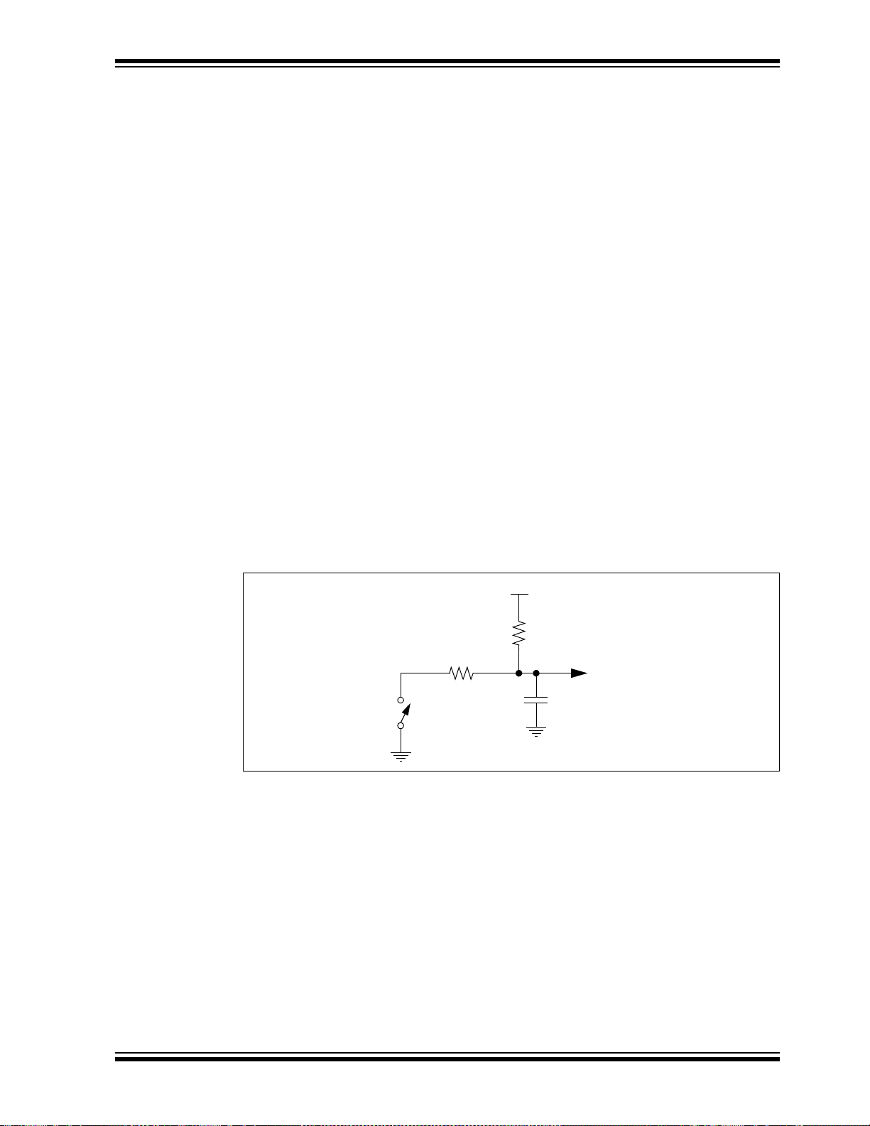
3.7 LESSON 6: DEBOUNCE
+V
R1
R2
Filtered
Switch
Output
SW
C
1
3.7.1 Introduction
Mechanical switches play an important and extensive role in practically every computer, microprocessor and microcontroller application. Mechanical switches are inexpensive, simple and reliable. In addition, switches can be very noisy. The apparent
noise is caused by the closing and opening action that seldom results in a clean electrical transition. The connection makes and breaks several, perhaps even hundreds, of
times before the final switch state settles.
The problem is known as switch bounce. Some of the intermittent activity is due to the
switch contacts actually bouncing off each other. Imagine slapping two billiard balls
together. The hard non-resilient material does not absorb the kinetic energy of motion.
Instead, the energy dissipates over time and friction in the bouncing action against the
forces pushing the billiard balls together. Hard metal switch contacts react in much the
same way. Also, switch contacts are not perfectly smooth. As the contacts move
against each other, the imperfections and impurities on the surfaces cause the electrical connection to be interrupted. The result is switch bounce.
The consequences of uncorrected switch bounce can range from being just annoying
to catastrophic. For example, imagine advancing the TV channel, but instead of getting
the next channel, the selection skips one or two. This is a situation a designer should
strive to avoid.
Switch bounce has been a problem even before the earliest computers. The classic
solution involved filtering, such as through a resistor-capacitor circuit, or through resetting table shift registers. These methods are still effective, but they involve additional
cost in material, installation and board real estate.
Lessons
FIGURE 3-5: SWITCH DEBOUNCING
One of the simplest ways to switch debounce is to sample the switch until the signal is
stable or continue to sample the signal until no more bounces are detected. How long
to continue sampling requires some investigation. However, 5 ms is usually plenty long,
while still reacting fast enough that the user will not notice.
The switch on the LPC Demo Board does not bounce much, but it is good practice to
debounce all switches in the system.
3.7.2 Hardware Effects
When the switch is held down, DS1 will be lit. When the switch is not held down, all
LEDs are OFF.
2012 Microchip Technology Inc. DS41628B-page 63
Page 64

PICkit™ 3 Starter Kit User’s Guide
#define SWITCH PORTA, 3 ;pin where SW1 is connected..NOTE: always READ from
the PORT and WRITE to the LATCH
#define LED LATC, 0 ;DS1
bsf LATC, 0 ;turn on the LED
bsf LED ;turn on the LED
MainLoop:
banksel PORTA ;get into Bank0
btfsc SWITCH ;defined above....notice how the PORT is being read and not the LATCH
bra LedOff ;switch is not pressed - turn OFF the LED
bra Debounce ;switch is held down, pin needs to be debounced
3.7.3 Summary
This lesson uses a simple software delay routine to avoid the initial noise on the switch
pin. The code will delay for only 5 ms, but should overcome most of the noise. The
required delay amount differs with the switch being used. Some switches are worse
than others.
This lesson also introduces the #define preprocessing symbol in both ‘C’ and assembly. Hard coding pin locations is bad practice. Values that may be changed in the future
should always be defined once in preprocessing. Imagine if another user wanted to use
these lessons in a different PIC device and all of the pins changed! This would require
going into the code and finding every instance of any pin reference.
EXAMPLE 3-28:
Now all that is needed is to change this one line and it will be reflected everywhere it is
used.
EXAMPLE 3-29:
The preprocessor will substitute LATC, 0 every time the LED identifier is seen. This is
done before the code is assembled/compiled, or rather processed, hence the name
preprocessor.
3.7.4 New Registers
Nothing new.
3.7.5 New Instructions
Nothing new.
3.7.6 Assembly
3.7.6.1 ENHANCED MID-RANGE
There is only one important main difference in this lesson from previous ones. Notice
how the port is being read, and not the latch, when the program is checking the switch.
If LATC is substituted in where PORTC is, the switch will never be detected. Remember
to read from the port and write to the latch. Read-modify-write operations on the LATC
register will read and write the latched output value for PORTC.
3.7.7 PIC18
Nothing new.
3.7.8 C Language
Nothing new.
DS41628B-page 64 2012 Microchip Technology Inc.
Page 65

3.8 LESSON 7: REVERSIBLE VARIABLE SPEED ROTATE
Get ADC Measurement
Delay Using ADC Result
Delay 5ms
Is Sw itch Still Down?
Check if ADC Result is ‘0’
Is Switch Down?
Change Direction
YES
YES
NO
Main Init
Was It Held Down Previously?
Rotate LE Ds to Left
Rotate LE Ds to Right
Left Direction
YES NO
YES
NO
NO
3.8.1 Introduction
This lesson combines all of the previous lessons in using the button to reverse the
direction of rotation when the button is pressed. The speed of rotation is controlled
using the potentiometer.
3.8.2 Hardware Effects
LEDs will rotate at a speed that is proportional to the ADC value. The switch will toggle
the direction of the LEDs.
3.8.3 Summary
The program needs to keep track of rotation direction and new code needs to be added
to rotate in the other direction. Lesson 5 rotates right and checks for a ‘1’ in the carry
bit to determine when to restart the sequence. In Lesson 7, the program needs to rotate
both ways and check for a ‘1’ in bit 4 of the display when rotating to the left. When the
‘1’ shows up in bit 4 of LATC, it will be re-inserted into bit 0.
FIGURE 3-6: PROGRAM FLOW FOR LESSON 7
Lessons
2012 Microchip Technology Inc. DS41628B-page 65
Page 66

PICkit™ 3 Starter Kit User’s Guide
76543210
00010111
00101110
MSb
LSb
RotateRight:
lslf LATC, f ;logical shift left
btfsc LATC, 4 ;did it rotate out of the LED display?
bsf LATC, 0 ;yes, put in bit 0
bra MainLoop
The debounce routine is more in-depth in this lesson because we need to keep in mind
of the scenario of the switch being held down for long periods of time. If SW1 is held
down, the LEDs would change direction rapidly, making the display look like it is out of
control. The above flowchart will only change direction on the first indication of a solid
press and then ignore the switch until it is released and pushed again. The switch must
be pressed for at least the time it takes for the program to check the switch in its loop.
Since the PIC MCU is running at 500 kHz, this will seem instantaneous.
3.8.4 New Registers
None.
3.8.5 New Instructions
3.8.5.1 PIC18
TABLE 3-27:
Instruction English Purpose
RLNCF Rotate left with no carry Shift bits to the left
3.8.5.1.1 rlncf
This rotates bits to the left without using the carry bit. The LSb simply becomes the
previous MSb. This is usually referred to as a circular shift.
EXAMPLE 3-30:
FIGURE 3-7: ROTATE LEFT WITHOUT CARRY
3.8.6 Assembly
3.8.6.1 ENHANCED MID-RANGE
Instead of using the carry bit to check if the LEDs are out of display range, the latch is
shifted to the left and LATC4 is checked. LATC4 is not connected to anything and if this
is ever set, it means that DS4 was just lit and now DS1 needs to be lit to repeat the
pattern. The PIC18 version is similar, but instead uses rlncf instead of lslf.
3.8.6.2 PIC18
The PIC18 always has to make sure that the carry bit is cleared once it is checked,
otherwise more than one LED may become lit.
DS41628B-page 66 2012 Microchip Technology Inc.
Page 67

EXAMPLE 3-31:
RotateLeft:
bcf STATUS, C ;clear the carry
rrcf LATC,f ;rotate the LEDs (through carry) and turn on the next LED to the right
btfss STATUS,C ;did the bit rotate into the carry (i.e. was DS1 just lit?)
bra MainLoop
bsf LATC, 3 ;yes, it did and now start the sequence over again by turning on DS4
bcf STATUS, C ;clear the carry
bra MainLoop ;repeat this program forever
unsigned char _previous_state = SWITCH_UP; //global variable
void main(void) {
unsigned char delay;
unsigned char direction;
.....
}
unsigned char check_switch(void){
...
..
}
Lessons
3.8.7 C Language
3.8.7.1 BOTH
This version utilizes global variables. Unlike local variables, global variables have no
function scope, meaning that they are visible to every function within the same source
file where it is declared. It is good practice to uniquely identify global variables such as
preceding each variable with an underscore.
This byte is modified in the check_switch function, and the result is returned to the
main loop.
EXAMPLE 3-32:
Notice how the bytes, delay and direction, were declared inside of main. These cannot
be modified anywhere outside of main. Also, notice how check_switch returns an
unsigned char byte to the main loop. In ‘C’, only one variable can be returned.
2012 Microchip Technology Inc. DS41628B-page 67
Page 68

PICkit™ 3 Starter Kit User’s Guide
3.9 LESSON 8: PULSE-WIDTH MODULATION (PWM)
3.9.1 Introduction
This lesson does not rely on any of the previous lessons, but does use the same coding
techniques and information learned thus far.
In this lesson, a PIC MCU generates a PWM signal that lights an LED with the POT
thereby controlling the brightness.
3.9.2 Hardware Effects
Rotating the POT will adjust the brightness of a single LED.
3.9.3 Summary
Pulse-Width Modulation (PWM) is a scheme that provides power to a load by switching
quickly between fully on and fully off states. The PWM signal resembles a square wave
where the high portion of the signal is considered the on state and the low portion of
the signal is considered the off state. The high portion, also known as the pulse width,
can vary in time and is defined in steps. A longer, high on time will illuminate the LED
brighter. The frequency or period of the PWM does not change. A larger number of
steps applied, which lengthens the pulse width, also supplies more power to the load.
Lowering the number of steps applied, which shortens the pulse width, supplies less
power. The PWM period is defined as the duration of one complete cycle or the total
amount of on and off time combined.
PWM resolution defines the maximum number of steps that can be present in a single
PWM period. A higher resolution allows for more precise control of the pulse width time
and, in turn, the power that is applied to the load. In this lesson, the program will be
using 10 bits of resolution – the maximum allowed.
The term duty cycle describes the proportion of the on time to the off time and is
expressed in percentages, where 0% is fully off and 100% is fully on. In this situation,
a lower duty cycle corresponds to less power applied and a higher duty cycle
corresponds to more power applied.
3.9.4 New Registers
3.9.4.1 BOTH
TABLE 3-28: NEW REGISTERS FOR BOTH DEVICES
Register Purpose
CCPXCON Setup of the “compare-capture-PWM” module
PRX The PWM period is specified by the PRx register of Timer2/4/6
CCPTMRS Selects what timer module is used in association with the PWM
CCPRXL Upper 8 bits (MSb) of PWM
TXCON Timer control register
3.9.4.1.1 All
The PIC16F1829 has two CCP modules and this lesson will use CCP2, while the
PIC18F14K22 only has one CCP module, so it will use CCP1.
It is recommended that the reader refer to the Capture/Compare/PWM section in the
data sheet to learn about each register above. This lesson will briefly cover how to
setup a single PWM.
Figure 3-8 summarizes how the PWM waveform is setup:
DS41628B-page 68 2012 Microchip Technology Inc.
Page 69

Lessons
Period
Pulse Width
TMRx = 0
TMRx = CCPRxH:CCPxCON<5:4>
TMRx = PRx
;PWM Period = [PR2 + 1]*4*Tosc*T2CKPS = [255=6+ 1]*4*(1/500kHz) * 1
Resolution
4 PRx 1+log
2log
------------- ------------- ------------ --- bits=
FIGURE 3-8: PWM ANALYSIS
The PWM period is specified by the PRx register. Timer 2/4/6 is used to count up to the
value in CCPRxH combined with two LSbs in CCPxCON. CCPRxL is used to load
CCPRxH. One can think of CCPRxL as a buffer which can be read or written to, but
CCPRxH is read-only. When the timer is equal to PRx, the following three events occur
on the next increment cycle:
1. TMRx is cleared
2. The CCPx pin is set
3. The PWM duty cycle is latched from CCPRxL into CCPRxH
The following steps should be executed in the order shown when configuring the CCP
module for standard PWM operation:
1. Select the Timer2/4/6 resource to be used for PWM generation by setting the
CxTSEL<1:0> bits in the CCPTMRS register.
2. Disable the CCPx pin output driver by setting the associated TRIS bit.
3. Load the PRx register with the PWM period value.
4. Configure the CCP module for the PWM mode by loading the CCPxCON register
with the appropriate values
5. Load the CCPRxL register and the DCxBx bits of the CCPxCON register, with the
PWM duty cycle value.
6. Configure and start Timer2/4/6:
a) Clear the TMRxIF interrupt flag bit of the PIRx register.
b) Configure the TxCKPS bits of the TxCON register with the Timer prescale
value.
c) Enable the Timer by setting the TMRxON bit of the TxCON register.
7. Enable PWM output pin.
This lesson uses a frequency of 486 Hz. Anything over ~60 Hz will eliminate any noticeable flicker.
EXAMPLE 3-33:
The designer should also consider the PWM resolution.
EQUATION 3-3: PWM RESOLUTION
Two conditions must hold true for this lesson:
1. 10 bits of resolution
2. No flicker in LED
2012 Microchip Technology Inc. DS41628B-page 69
Page 70

PICkit™ 3 Starter Kit User’s Guide
Both devices are using some features of the enhanced PWM module. The PIC16 will
operate the CCP module in single output since the CCP2 P2A pin connects directly to
DS4. The PIC18 will operate the CCP module in Full-Bridge mode in order to modulate
P1D on DS3.
Maximum resolution is achieved when the PRx register is set to 0xFF, or rather 255,
the maximum value an 8-bit number can hold.
Below is a scope capture of the PWM signal when the LED is dimly lit. As one can see,
the Period is around ~2 ms, with the pulse width being only few hundred us wide.
FIGURE 3-9: SMALL PULSE WIDTH
Figure 3-10 shows when the dial is turned 30% clockwise. Notice how the pulse width
is greater than that shown in Figure 3-9, and that the frequency did not change.
FIGURE 3-10: GREATER PULSE WIDTH
TABLE 3-29:
Instruction English Purpose
andlw And a literal with WREG Masking values
DS41628B-page 70 2012 Microchip Technology Inc.
Page 71

EXAMPLE 3-34:
call A2d ;begin the Analog to Digital conversion
;ADRESH and ADRESL are now both full of the ADC result!
movf ADRESH, w ;Get the top 8 MSbs (remember that the ADC result is LEFT justified!)
banksel CCPR2L
movwf CCPR2L
;to fill all 10 bits of the duty cycle, the 2 LSbs will be put into the
;Duty Cycle Bits (DC2B) of the CCP2CON register which are bits 5 and 4.
;So we need to shift these LSb into place and OR them with CCP2CON
; in order to save the control settings above and fill these last bits in
banksel ADRESL
;ADRESL = b'xx000000' where 'xx' are the 2 LSbs from the
;ADC result
lsrf ADRESL, f ;ADRESL = b'0xx00000'
lsrf ADRESL, f ;ADRESL = b'00xx0000'
movf ADRESL, w ;now move into wreg
banksel CCP2CON
xorwf CCP2CON, w ;move the 2 LSbs into place without disturbing the rest of
;CCP2CON settings
andlw B'00110000'
xorwf CCP2CON, f
bra MainLoop ;do this forever
EXAMPLE 3-35:
Lessons
3.9.5 Assembly
3.9.5.1 ENHANCED MID-RANGE
This fills the eight MSbs in the PWM register. The next few lines can be commented out
and still provide the same perceived output. This is because the two LSbs do not play
a significant role in terms of duty cycle resolution. This lesson uses all ten bits for completeness.
In Example 3-35, the program shifts the ADRESL register, which contains the two LSbs
from the ADC result. Bits <5:0> are always cleared while bits <7:6> contain part of the
ADC result. The PIC MCU will simply shift this register to the right twice so that they are
in bits <5:4>. Notice how the result of the shift is saved in ADRESL and NOT in WREG.
In the next three instructions: the first XOR clears bits that are the same and sets bits
that are different. The result is in WREG. The next AND function clears all control bits
in WREG, so they do not change in the final step. The final XOR changes the bits that
changed and leaves everything else untouched. The result is saved to the CCP2CON
register. A movwf or iorwf would not work, since it would not preserve the settings
applied in the initialization.
3.9.5.2 PIC18
The PIC18 substitutes the rrncf instruction with the lsrf instruction above, although
2012 Microchip Technology Inc. DS41628B-page 71
a rrcf would also work.
3.9.5.3 C LANGUAGE
Nothing new.
Page 72

PICkit™ 3 Starter Kit User’s Guide
3.10 LESSON 9: TIMER0
3.10.1 Introduction
This lesson will produce the same output as 3.4 “Lesson 3: Rotate ”. The only difference is that this version uses Timer0 to provide the delay routine.
3.10.2 Hardware Effects
LEDs rotate from right to left, similar to Lesson 3.
3.10.3 Summary
Timer0 is a counter implemented in the processor. It may be used to count instruction
cycles or external events, that occur at or below the instruction cycle rate.
In the PIC18, Timer0 can be used as either an 8-bit or 16-bit counter, or timer. The
enhanced mid-range core implements only an 8-bit counter.
This lesson configures Timer0 to count instruction cycles and to set a flag when it rolls
over. This frees up the processor to do meaningful work rather than wasting instruction
cycles in a timing loop.
Using a counter provides a convenient method of measuring time or delay loops as it
allows the processor to work on other tasks rather than counting instruction cycles.
3.10.4 New Registers
3.10.4.0.1 Enhanced Mid-range
TABLE 3-30: ENHANCED MID-RANGE NEW REGISTER
Register Purpose
OPTION_REG Timer0 and pull-up/INT configuration
DS41628B-page 72 2012 Microchip Technology Inc.
Page 73

Lessons
btfss INTCON, TMR0IF ;did TMR0 roll over yet?
bra $-1 ;wait until TMR0 overflows and sets TMR0IF
bcf INTCON, TMR0IF ;must clear flag in software
;rotate the LEDs
.....
3.10.4.0.2 OPTION_REG
This register controls Timer0 settings as well as some miscellaneous features, such as
weak pull-ups, which will be used in later lessons.
3.10.4.1 PIC18
TABLE 3-31: NEW REGISTERS FOR PIC18
Register Purpose
T0CON Timer0 configuration
3.10.4.1.1 T0CON
The T0CON register and OPTION_REG are similar with respect to the prescaler settings and Timer0 assignment bits. The enhanced mid-range Timer0 is always enabled,
so there is no need to enable it. The weak pull-ups and INT detection are performed in
separate registers on the PIC18.
Timer0 will generate an interrupt when the TMR0 register overflows from 0xFF to 0x00
(if in 8-bit mode for the PIC18). The TMR0IF interrupt flag bit of the INTCON register is
set every time the TMR0 register overflows, regardless of whether or not the Timer0
interrupt is enabled. The TMR0IF bit can only be cleared in software. The Timer0 interrupt enable is the TMR0IE bit of the INTCON register.
EXAMPLE 3-36:
3.10.5 Assembly
3.10.5.1 PIC16
The MainLoop label of the program will simply wait for the timer to overflow. When it
does, it will clear the flag and shift the LEDs. The flag MUST be cleared in software. If
this lesson is compared with Lesson 3, the reader should notice a reduction in code,
and that it is easier to follow. Timers greatly simplify delay loops and are great for
events that need precise timing.
3.10.5.2 PIC18
The only differences are that the initialization is slightly different and the relative branch
uses “$-2”.
3.10.6 C Language
Nothing new.
2012 Microchip Technology Inc. DS41628B-page 73
Page 74

PICkit™ 3 Starter Kit User’s Guide
Ms
Global Interrupt Enable
Other Interrupt Sources
Interrupt Flag
Interrupt Enable
3.11 LESSON 10: INTERRUPTS AND PULL-UPS
3.11.1 Introduction
This lesson introduces interrupts and how they are useful. It also introduces internal
weak pull-ups that are available on most PIC devices. This lesson expands on the previous lessons, but mostly Lessons 9 and 3.
3.11.2 Hardware Effects
LEDs rotate at a constant speed and the switch reverses their direction.
3.11.3 Summary
Two new concepts are introduced: interrupts and weak pull-ups.
3.11.3.1 INTERRUPTS
The interrupt feature allows certain events to preempt normal program flow. This
means that the microcontroller can be configured to be aware of its surroundings. Routines can be run upon some external event. Firmware is used to determine the source
of the interrupt and act accordingly. All interrupts can be configured to wake the MCU
from Sleep mode.
Most of the peripherals can generate an interrupt. Some of the I/O pins may be configured to generate an interrupt when they change state. When a peripheral needs service, it sets its interrupt flag. Each interrupt flag is ANDed with its enable bit and then
these are ORed together to form a master interrupt. This master interrupt is ANDed with
the Global Interrupt Enable (GIE). The enable bits allow the PIC microcontroller to limit
the interrupt sources to certain peripherals. See the Interrupt Logic Figure in the PIC
microcontroller data sheet for a drawing of the interrupt logic. Below is a simplified diagram.
FIGURE 3-11: SUMMARY OF INTERRUPT FLOW
The PIC18 has a slightly different structure to accommodate interrupt priority. The
enhanced mid-range core has only one interrupt vector. This means that whenever an
interrupt occurs, the program counter goes to the interrupt service address, specifically
address 0x0004. The PIC18 allows most interrupt sources to be assigned a high or low
priority level. The high priority vector is at 0x0008 and the low at 0x0018. A high priority
interrupt event will interrupt a low priority that may be in progress. This lesson will not
utilize priority interrupts and will instead make use of the mid-range compatibility feature by clearing the IPEN bit. Both devices will now service from only one vector.
When an interrupt is responded to, the Global Interrupt Enable (GIE) bit is cleared to
disable further interrupts. The return address is pushed onto the stack and the PC is
loaded with the interrupt vector address. Both the enhanced mid-range and PIC18
devices perform automatic context saving for the WREG, STATUS, and BSR registers.
The FSR and PCLATH registers are saved only in the enhanced mid-range devices.
The PIC18 requires a retfie, fast instruction execution to restore the context.
DS41628B-page 74 2012 Microchip Technology Inc.
Page 75

Lessons
VDD
R2
Rpull-up
To P I C
®
MCU
SW1
GND
Irp
RA2
VI * R=
VA 3 140 * 106– * 2k 28mV==
The firmware within the Interrupt Service Routine (ISR) should determine the source of
the interrupt by polling the interrupt flag bits. The serviced interrupt flag bits must be
cleared before exiting the ISR to avoid repeated interrupts. Because the GIE bit is
cleared, any interrupt that occurs while executing the ISR will be recorded through its
interrupt flag, but will not cause the processor to redirect to the interrupt vector until the
retfie instruction is executed, thereby enabling the GIE bit.
3.11.3.2 WEAK PULL-UPS
Both the enhanced mid-range and PIC18 devices in this tutorial are able to provide
internal pull-up resistors on some pins. This can greatly reduce the need of external
hardware.
FIGURE 3-12: WEAK PULL-UP DIAGRAM
As seen in Figure 3-12, by enabling the weak pull-up on a pin, the pin will always read
a ‘1’ if no other external circuitry is connected to RA2. In this demo, there is a resistor
connected to the switch, which is then connected to ground. When the switch is
pressed, the voltage on RA2 is no longer V
DD, but rather close to 0V, or ground.
The pull-up resistor is not given a value in the electrical specifications, but rather the
current, Ipur. For the PIC16F1829, this is typically 140 µA. When the switch is closed,
given the typical current spec, the voltage on RA2 becomes:
EQUATION 3-4:
It is called a “weak” pull-up since it does not bring the pin to V
pull-up would have a low resistance and bring the pin quickly up to V
DD quickly. A stronger
DD. If there is a fair
amount of capacitance on the pin, the pin may take a while to register as logic-high to
the PIC MCU. Since it is a weak pull-up, the designer can easily override this internal
setting by using an external resistor, typically in the range of 1k-10k, to change the pin’s
state.
2012 Microchip Technology Inc. DS41628B-page 75
Page 76

PICkit™ 3 Starter Kit User’s Guide
Rising Edge
Falling Edge
3.11.4 New Registers
3.11.4.1 BOTH
TABLE 3-32: NEW REGISTERS FOR BOTH DEVICES
Register Purpose
WPUA Weak pull-up enable
This enables the individual internal pull-up circuitry for each pin on PORTA.
3.11.4.2 ENHANCED MID-RANGE
TABLE 3-33: NEW REGISTERS FOR ENHANCED MID-RANGE
Register Purpose
IOCAN Interrupt-on-change PORTA negative edge
IOCAF Interrupt-on-change PORTA flags
3.11.4.2.1 IOCAN/IOCAF
The PIC16F1829 can detect rising and falling edge interrupts. IOCAN contains the negative edge detection enable bits and IOCAF contains the interrupt flags. This lesson
enables the switch input as an interrupt-on-change pin through IOCAN and clears all
the flags in IOCAF inside the ISR.
This lesson uses the interrupt-on-change peripheral, which causes the PIC MCU to go
to address 0x0004 (interrupt vector), when RA2 changes from a high-to-low state.
FIGURE 3-13: RISING/FALLING EDGES
3.11.4.3 PIC18
TABLE 3-34: NEW REGISTERS FOR PIC18
Register Purpose
IOCA Interrupt-on-change PORTA (both edges)
RCON Detects what caused the interrupt
3.11.4.3.1 IOCA
The PIC18F14K22 does not have a negative and positive edge trigger, but rather just
one that detects both. More software is needed to determine which edge occurred.
3.11.4.3.2 RCON
The RCON register is used to detect what caused the PIC MCU to reset as well as
enable/disable priority interrupts. This lesson shows how to use this register to disable
priority interrupts.
DS41628B-page 76 2012 Microchip Technology Inc.
Page 77

EXAMPLE 3-37:
MainLoop:
bra MainLoop ;can spend rest of time doing something critical here
Org 0x0 ;Reset Vector starts at 0x0000
bra Start ;main code execution
ORG 0x0004 ;Interrupt Vector starts at address 0x0004
goto ISR
;Enter here if an interrupt has occurred
;First, check what caused the interrupt by checking the ISR flags
;This lesson only has 2 flags to check
ISR:
banksel IOCAF ;bank7
btfsc IOCAF, 3 ;check the interrupt-on-change flag
bra Service_SW1 ;switch was pressed
bra Service_TMR0 ;Timer0 overflowed
Lessons
3.11.5 New Instructions
3.11.5.1 BOTH
TABLE 3-35: NEW INSTRUCTIONS FOR BOTH DEVICES
Instruction English Purpose
retfie Return from interrupt Return to normal execution
3.11.5.1.1 retfie
The retfie instruction exits the ISR by popping the previous address from the stack
and setting the GIE bit. The PIC18 requires the retfie, fast instruction to restore
the saved context, whereas the enhanced mid-range does not have this distinction.
3.11.6 Assembly
3.11.6.1 BOTH
By using interrupts, the main loop can spend time doing other things such as crunching
numbers or writing to an LCD. The program no longer needs to wait for the flag to
become set to continue like the previous lesson did. This example code will simply
branch to MainLoop indefinitely, doing nothing while waiting for the interrupt.
EXAMPLE 3-38:
EXAMPLE 3-39:
3.11.6.2 ENHANCED MID-RANGE
This jumps to the ISR routine. Notice how the goto statement is directly after the interrupt vector address.
Inside the ISR, the cause of the interrupt is determined. Once determined, one of the
services that must be completed is clearing the interrupt flag so that the ISR can be
successfully left. The retfie instruction exits the ISR by restoring the saved context,
re-enables the GIE bit and returns to the instruction following the last instruction
executed when the interrupt occurred.
2012 Microchip Technology Inc. DS41628B-page 77
Page 78

PICkit™ 3 Starter Kit User’s Guide
#ifdef PULL_UPS
banksel WPUA
bsf WPUA, 2 ;enable the weak pull-up for the switch
banksel OPTION_REG
bcf OPTION_REG, NOT_WPUEN ;enable the global weak pull-up bit
;this bit is active HIGH, meaning it must be cleared for it to be enabled
#endif
Org 0x0000 ;Reset Vector starts at 0x0000
bra Start ;main code execution
Org 0x0008 ;High Priority Interrupt Vector starts at address 0x0008
goto ISR
#ifdef PULL_UPS
bsf WPUA, 2 ;enable the weak pull-up for the switch
bcf INTCON2, NOT_RABPU ;enable the global weak pull-up bit
;this bit is active HIGH, meaning it must be cleared for it to be enabled
#endif
EXAMPLE 3-40:
The #ifdef is a preprocessor directive, which will look to see if the directive, in this
case PULL_UPS, is defined. If so, the code between the #ifdef and #endif will be
assembled. These two lines activate the weak pull-up resistor on pin RA2.
3.11.6.3 PIC18
The PIC18 does not differentiate between rising and falling edges. Therefore, the same
debounce routine and flowchart in Lesson 7 (Figure 3-6) will be used.
EXAMPLE 3-41:
EXAMPLE 3-42:
When priority interrupts are disabled, all interrupts occur at address 0x0008.
Same as the PIC16, except that the registers and bit names are changed slightly.
3.11.7 C Language
The enhanced core can have only one interrupt vector defined. This is done by creating
a function with the interrupt keyword:
void interrupt ISR(void)
This is a special name and is reserved only for the ISR. The PIC18 can have two, but
this lesson uses only one as shown above.
DS41628B-page 78 2012 Microchip Technology Inc.
Page 79

3.12 LESSON 11: INDIRECT ADDRESSING
3.12.1 Introduction
This lesson covers a very important topic of indirect addressing. The code uses indirect
addressing to implement a moving average filter. This lesson adds a moving average
filter to the Analog-to-Digital code in Lesson 4. The moving average keeps a list of the
last ADC values (n) and averages them together. The filter needs two parts: A circular
queue and a function to calculate the average.
Twisting the potentiometer changes the value read by the Analog-to-Digital converter.
The filtered value is then sent to the LED display.
The filter averages the last eight readings. Choosing a power of two for the number of
samples allows division by simple rotates instead of a general purpose divide routine.
Rather than summing the array every time, it is faster to keep a running sum, then
subtract out the oldest value in the queue and add in the new value.
FIGURE 3-14: MOVING AVERAGE WITH INDIRECT ADDRESSING
Lessons
3.12.2 Hardware Effects
This lesson provides the same outcome as Lesson 4. The user rotates the POT to see
the LEDs rotate. The top four MSbs of the ADC value are reflected onto the LEDs.
3.12.3 Summary
While the program memory can be addressed in only one way – through the program
counter – information in the data memory space can be addressed in several ways. For
most instructions, the addressing mode is fixed. Other instructions may use up to three
modes, depending on which operands are used and whether or not the extended
instruction set is enabled.
2012 Microchip Technology Inc. DS41628B-page 79
Page 80

PICkit™ 3 Starter Kit User’s Guide
The addressing modes are:
1. Inherent
2. Literal
3. Direct
4. Indirect
3.12.3.1 INHERENT AND LITERAL
Many PIC device control instructions do not need any argument at all; they either
perform an operation that globally affects the device or they operate implicitly on one
register. This addressing mode is known as Inherent Addressing. Examples include
SLEEP and RESET, which are used in the EEPROM lesson.
Other instructions work in a similar way but require an additional explicit argument in
the opcode. This is known as Literal Addressing mode because they require some
literal value as an argument. Examples include addlw, movlb, call, and goto.
3.12.3.2 DIRECT ADDRESSING
Direct addressing specifies all or part of the source and/or destination address of the
operation within the opcode itself. The options are specified by the arguments
accompanying the instruction. In the core PIC device instruction set, bit-oriented and
byte-oriented instructions use some version of direct addressing by default. All of these
instructions include a 7-bit (8-bit for PIC18) literal address in their Least Significant
Byte. This address specifies either a register address in one of the banks of data RAM
or a location in the Access Bank (if using the PIC18) as the data source for the
instruction.
The destination of the operation’s results is determined by the destination bit ‘d’. When
‘d’ is ‘1’, the results are stored back in the source register, overwriting its original
contents. When ‘d’ is ‘0’, the results are stored in the WREG register.
3.12.3.3 INDIRECT ADDRESSING
Indirect addressing allows the user to access a location in data memory without giving
a fixed address in the instruction. This is done by using File Select Registers (FSRs)
as pointers to the locations which are to be read or written. Since the FSRs are
themselves located in RAM as Special File Registers, they can also be directly
manipulated under program control. This makes FSRs very useful in implementing
data structures, such as tables and arrays in data memory. The registers for indirect
addressing are also implemented with Indirect File Operands (INDFs) that permit
automatic manipulation of the pointer value with auto-incrementing, auto-decrementing
or offsetting with another value.
The INDFn registers are not physical registers. These can be thought of as “virtual”
registers: they are mapped in the SFR space, but are not physically implemented.
Reading or writing to a particular INDF register actually accesses its corresponding
FSR register pair. A read from INDF1, for example, reads the data at the address
indicated by FSR1H:FSR1L.
DS41628B-page 80 2012 Microchip Technology Inc.
Page 81

3.12.4 New Registers
Indirect AddressingDirect Addressing
Bank Select
Location Select
4 BSR 6
0
From Opcode
FSRxL7 0
Bank Select
Location Select
00000 00001 00010 11111
0x00
0x7F
Bank 0 Bank 1 Bank 2 Bank 31
0
FSRxH7 0
0 0 0 0
3.12.4.1 BOTH
TABLE 3-36: NEW REGISTERS FOR BOTH DEVICES
Register Purpose
INDFx Virtual indirect register
FSRx Holds target address of virtual register
3.12.4.1.1 INDFx/FSRx
Because indirect addressing on both the PIC18 and enhanced mid-range core use the
full address range, data RAM banking is not necessary. The FSR registers on the
PIC18 form a 12-bit address while the enhanced mid-range forms a 16-bit address.
This means that the PIC18 FSR provides access to the whole data memory range,
while the enhanced mid-range gives access to all of the memory banks including
read-only access program memory.
FIGURE 3-15: ENHANCED MID-RANGE INDIRECT/DIRECT ADDRESSING
Lessons
2012 Microchip Technology Inc. DS41628B-page 81
3.12.5 New Instructions
3.12.5.1 BOTH
TABLE 3-37: NEW INSTRUCTIONS FOR BOTH DEVICES
incf Increment Add a value of one
Instruction English Purpose
3.12.5.1.1 incf
This increments a file register by a value of one.
Page 82

PICkit™ 3 Starter Kit User’s Guide
FilterInit:
movlw low Queue ;point to the Queue holding the ADC values
movwf FSR0L
movlw high Queue
movwf FSR0H
INDF0
Queue [7]
Address:
Value: ??????
Address: 0x000
Value: ??????
Address: 0x0054
Value[0]: d’15’
FSR0L:FSR0H
0x004:0x005
INDF0
Queue [7]
Address:
Value: 0x0054
Address: 0x000
Value: d’15’
Address: 0x0054
Value[0]: d’15’
FSR0L:FSR0H
0x004:0x005
rrcf RunningSum,w ; divide by 2 and copy to a version we can corrupt
3.12.6 Assembly Language
3.12.6.1 BOTH
EXAMPLE 3-43:
Here, FSR0 is pointed towards the Queue location. Figure 3-16 explains the code in
Figure 3-43. It is important to note that FSR0 is two bytes wide in order to address
locations in program memory across multiple pages.
FIGURE 3-16: BEFORE FILTERINIT IS CALLED
FIGURE 3-17: AFTER FILTERINIT IS CALLED
DS41628B-page 82 2012 Microchip Technology Inc.
After FilterInit is called, the FSR0 register is pointing towards the fist byte in
queue. The INDF0 register can now be read/written to. Any affects on the INDF0 register will affect the value at the assigned address in the FSR0 register. An increment of
FSR0 will point to the next byte in the Queue register. In this case, it is the second ADC
reading.
A rotate or shift to the right is a quick method to divide by two.
Page 83

EXAMPLE 3-44:
Before Rotate right: b'00001010'= d'10'
After Rotate right: b'00000101'= d'5'
while (1) {
ptr_queue = &queue; //point to the first byte in this array
(RESET the pointer)
for (i = NUM_READINGS; i != 0; i--){
LATC = (average(ptr_queue) >> 4 ); //only want the 4 MSbs for 4 LEDs
ptr_queue++;
unsigned char average(unsigned char *ptr) {
unsigned char adc_value;
_sum -= *ptr; //subtract the current value out of the sum
adc_value = adc();
*ptr = adc_value; //assign ADC value to the queue
_sum += adc_value; //add to the sum
return (_sum/NUM_READINGS); //compute the average
}
Lessons
EQUATION 3-5:
3.12.7 C language
3.12.7.1 BOTH
Pointers in ‘C’ are constructed by using the INDF/FSR pair on the PIC16/PIC18 to
achieve the effect.
Similar to the assembly version, the main loop starts by resetting the pointer by pointing
(referencing) to the first byte in the queue. Then, an ADC reading is taken and saved
in the queue. LATC is then assigned the average of the queue. Remember that ‘queue’
is eight bytes wide, so it can hold eight samples of the ADC result (two LSbs of the
result are not saved).
EXAMPLE 3-45:
The average function has the pointer to queue as a parameter. The _sum is a global
variable which retains its value outside of this function. The current value in the running
sum is subtracted. The asterisk means that its value is being used (dereferencing). A
new ADC value is taken and added back into the running sum and the queue. The average reading is then returned to the main loop to be shifted onto the LED display.
There is a great deal of information about pointers for the ‘C’ language on the web. It
is recommended that the reader look there for additional information.
2012 Microchip Technology Inc. DS41628B-page 83
Page 84

PICkit™ 3 Starter Kit User’s Guide
y = function(x);
3.13 LESSON 12: LOOK-UP TABLE
3.13.1 Intro
It is sometimes useful to implement a table to convert from one value to another.
Expressed in a high-level language it might look like this:
EQUATION 3-6:
That is, for every value of x, the function returns the corresponding y value. Look-up
tables are a fast way to convert an input to meaningful data because the transfer function is pre-calculated and “looked up”, rather than calculated on the fly. A function that
converts hexadecimal numbers to the ASCII equivalent is one such example.
The great benefit of using a look-up table is that abundant Flash memory is used to
store constant values in lieu of the more limited RAM space. This allows greater flexibility and expands the memory capability of the program.
3.13.2 Hardware Effects
Gray coded binary will be reflected on the LEDs in accordance with the POT reading.
3.13.3 Summary
This lesson shows multiple ways to access program memory. The table simply converts
from regular binary code to the gray code equivalent. Gray codes are frequently used
in encoder applications to avoid wild jumps between states.
Binary encoders are typically implemented an opaque disk sensed by light sensors.
Due to different threshold levels on different bits, bits may change at slightly different
times, yielding momentary invalid results. Gray code prevents invalid transitions,
because only one bit changes from one sequence to the next. The current code is
correct until it transitions to the next.
The algorithm to convert between binary and Gray code is fairly complex. For a small
number of bits, the table look-up is smaller and faster.
3.13.4 New Registers
3.13.4.1 BOTH
TABLE 3-38: NEW REGISTERS FOR BOTH DEVICES
Register Purpose
PCL Program Counter (PC) Least Significant Byte
PCLATH Write Buffer for the higher 7 bits of the Program Counter (8 bits for PIC18)
The PC addresses bytes in the program memory. Recall that the enhanced PIC16 has
a Program Counter size of 15 bits and the PIC18 has a Program Counter of 21 bits.
The two devices share the offset implementation rather closely still.
3.13.4.1.1 PCL:
The low byte, known as the PCL register, is both readable and writable. The high byte,
or PCH register is not directly readable or writable. Updates to this register are performed through the PCLATH register.
For the PIC18, the PC contains another register called PCU. This register contains the
PIC18’s PC<20:16> bits; it is also not directly readable or writable. Updates to the PCU
register are performed through the PCLATU register.
DS41628B-page 84 2012 Microchip Technology Inc.
Page 85

Lessons
3.13.4.1.2 PCLATH:
The contents of PCLATH and PCLATU (if using the PIC18) are transferred to the program counter by any operation that writes PCL. Similarly, the upper two bytes of the
program counter are transferred to PCLATH and PCLATU by an operation that reads
PCL. This is useful for the computed offsets to the PC that are used in this lesson.
For the PIC18, the PC increments by two to address sequential instructions in program
memory. The PC increments by one in the enhanced mid-range core. This can be seen
in previous lessons’ assembly where there was a dollar sign ($) with an offset literal.
The enhanced core assembly uses a $-1 to go back one valid program instruction in
program memory. Likewise, the PIC18 uses a $-2.
FIGURE 3-18: FIVE SITUATIONS FOR THE LOADING OF THE PC ON THE
ENHANCED MID-RANGE CORE
2012 Microchip Technology Inc. DS41628B-page 85
Page 86

PICkit™ 3 Starter Kit User’s Guide
3.13.5 New Registers
3.13.5.1 ENHANCED MID-RANGE
TABLE 3-39: NEW REGISTERS FOR ENHANCED MID-RANGE
Register Purpose
EEADRx Address to read/write in program or EEPROM memory
EEDATx 2-byte word that holds 14-bit data for read/write
EECON1 Control register for memory access
Flash program memory is also writable during normal operation. This is commonly
referred to as “Self-modifying code” or “Self-write”. This is achievable by implementing
a modified Harvard architecture.
3.13.5.1.1 EEADRx/EEDATx
When accessing the program memory block, the EEDATH:EEDATL register pair forms
a 2-byte word that holds the 14-bit data for read/write, and the EEADRL and EEADRH
registers form a 2-byte word that holds the 15-bit address of the program memory location being accessed.
3.13.5.1.2 EECON1
Control bit EEPGD determines if the access will be a program or data memory access.
When clear, any subsequent operations will operate on the EEPROM memory. When
set, any subsequent operations will operate on the program memory. On Reset,
EEPROM is selected by default.
Control bits RD and WR initiate read and write, respectively. These bits cannot be
cleared, only set, in software. They are cleared in hardware at completion of the read
or write operation. The inability to clear the WR bit in software prevents the accidental,
premature termination of a write operation.
The WREN bit, when set, will allow a write operation to occur. On power-up, the WREN
bit is clear.
3.13.5.2 PIC18
TABLE 3-40: NEW REGISTERS FOR PIC18
Register Purpose
TBLPTR Points to a byte address in program space
TABLAT Holds 8-bit data from program space
3.13.5.2.1 TBLPTR
The Table Pointer (TBLPTR) points to a byte address in program space. Executing
TBLRD places the byte pointed to into TABLAT. In addition, TBLPTR can be modified
automatically for the next table read operation.
The TBLPTR is comprised of three SFR registers: Table Pointer Upper Byte, Table
Pointer High Byte and Table Pointer Low Byte (TBLPTRU:TBLPTRH:TBLPTRL).
These three registers join to form a 22-bit wide pointer.
3.13.5.2.2 TABLAT
The Table Latch (TABLAT) is an 8-bit register mapped into the SFR space. The Table
Latch register is used to hold 8-bit data during data transfers between program memory
and data RAM.
DS41628B-page 86 2012 Microchip Technology Inc.
Page 87

Lessons
3.13.6 New Instructions:
3.13.6.1 BOTH:
TABLE 3-41: NEW INSTRUCTIONS FOR BOTH DEVICES
Instruction English Purpose
retlw Return with literal in WREG Table look-ups
3.13.6.1.1 retlw
The WREG register is loaded with the 8-bit literal specified as 8 bits in the instruction
word. The program counter is then loaded from the top of the stack (the return
address). Recall that the PIC MCU utilizes a modified Harvard architecture. It is modified because it allows the contents of the instruction memory to be accessed as if it
were data.
3.13.6.2 ENHANCED MID-RANGE
TABLE 3-42: NEW INSTRUCTIONS FOR ENHANCED MID-RANGE
Instruction English Purpose
moviw Move INDFx to WREG Shorthand movlw with increment/decrement
brw Relative with WREG Local jump table
3.13.6.2.1 moviw
This instruction is used to move data between WREG and one of the indirect registers
(INDFn). Before/after this move, the pointer (FSRn) is updated by pre/post incrementing/decrementing it.
Recall that the INDFn registers are not physical registers. Any instruction that accesses
an INDFn register actually accesses the register at the address specified by the FSRn.
FSRn is limited to the range 0000h-FFFFh. Incrementing/decrementing it beyond
these bounds will cause it to wrap around.
3.13.6.2.2 brw
The brw, relative branch, instruction adds an offset to the PC. brw allows relocatable
code and codes that cross page boundaries. This adds the contents of WREG
(unsigned) to the PC. Since the PC will have incremented to fetch the next instruction,
the new address will be PC + 1 + (WREG). The designer does not need to worry about
program memory boundaries being crossed when using this.
3.13.6.3 PIC18:
TABLE 3-43: NEW INSTRUCTIONS FOR PIC18
Instruction English Purpose
tblrd* Table Read Table look-up data retrieval
3.13.6.3.1 tblrd
This instruction is used to read the contents of program memory. To address the
program memory, a three-byte pointer called Table Pointer is used. All three bytes of
Table Pointer must be setup before executing the
tblrd* instruction.
2012 Microchip Technology Inc. DS41628B-page 87
Page 88

PICkit™ 3 Starter Kit User’s Guide
ANDLW 0x0F
FIGURE 3-19: TABLE POINTER USED TO READ ONE BYTE OF DATA –
ANSWER IS REFLECTED IN ‘TABLAT’
3.13.7 Assembly Language
3.13.7.1 ENHANCED MID-RANGE
There are three methods of accessing constants in program memory:
1. Computed goto
2. Indirect Addressing
3. Table Reads
The code will implement 3 different ways to utilize these methods:
1. Computed goto
a) Program Counter
b) BRW instruction
2. Indirect Addressing
a) FSR/INDF
3. Table Reads
a) EECON/EEDAT/EEADR SFRs
The third method can return the full 14 bits of the program memory words while the first
two only return an 8-bit byte. This lesson demonstrates all three methods, but utilizes
only the lower 8-bits of the data retrieved by method three.
3.13.7.1.1 Program Counter
Calling the look-up table has a limitation: if the table falls across a 256-byte page
boundary, or the index into the table exceeds the table bounds, then it will jump to a
location out of the table.
Good programming practices dictate a few additional instructions for our example: first,
since the table is only sixteen entries, make sure a number no larger than 16 is passed
in. The simplest way to do this is to logically AND the contents of WREG before modifying PCL:
More complex error recovery schemes may be appropriate, depending on your application.
In addition, there are some nuances to be aware of, should the table cross a 256-word
boundary. The Program Counter is 15 bits wide, but only the lower eight bits are represented in PCL. The remaining five bits are stored in PCLATH. However, an overflow of
DS41628B-page 88 2012 Microchip Technology Inc.
Page 89

EXAMPLE 3-46:
;Using the Program Counter (PC) directly
movlw high TableStart ; get high order part of the beginning of the table
movwf PCLATH
movlw low TableStart ; load starting address of table
addwf temp,w ; add offset from ADC conversion
btfsc STATUS,C ; did it overflow?
incf PCLATH,f ; yes: increment PCLATH
movwf PCL ; modify PCL
EnhancedMethod:
brw ;jumps ahead by the amount currently in wreg
TableStart:
retlw b'0000' ; 0
……
movlw high TableStart ; get high order part of the beginning of the table
movwf FSR0H
movlw low TableStart ; get lower order part of the table
addwf temp, w ; add offset from ADC conversion
btfsc STATUS, C ; did it overflow?
incf FSR0H, f ; yes: increment high byte
movwf FSR0L ; modify lower byte
moviw FSR0++ ; move the value that FSR0 is pointing to into wreg
return ; grey code now in wreg, return to MainLoop
EXAMPLE 3-47:
Lessons
the lower eight bits is not automatically carried over into PCLATH. Because of this, be
sure to check the Carry flag in the STATUS register immediately after the table offset
addition, so that the PCLATH can be modified accordingly.
3.13.7.1.2 brw instruction
Once the ADC value is loaded into WREG, the Program Counter can be modified in a
somewhat more indirect method than above. The program counter will be offset by the
value in the working register. This is the most efficient method for small tables.
EXAMPLE 3-48:
3.13.7.1.3 Indirect Addressing
The FSRx/INDFx pair can be used nicely in this example. Any large table look-ups
should follow this method.
The below code loads the starting address of the gray code table. Then, the ADC value
is added into FSR0 as the offset, which points to the corresponding gray code value.
3.13.7.1.4 Table Reads
This method uses special SFRs that are used strictly for Flash program memory
reads/writes. Writing to program memory is more complex and restrictive, but reading
a single word from program memory is straightforward.
2012 Microchip Technology Inc. DS41628B-page 89
Page 90

PICkit™ 3 Starter Kit User’s Guide
banksel EEADRL ; bank 3
movlw high TableStart ;
movwf EEADRH ; Store MSb of address
movlw low TableStart ;
addwf temp, w
btfsc STATUS, C
incf EEADRH, f
movwf EEADRL ; Store LSb of address
bcf EECON1, CFGS ; Do not select Configuration Space
bsf EECON1, EEPGD ; Select Program Memory
bcf INTCON, GIE ; Disable interrupts
bsf EECON1, RD ; Initiate read
nop ; Executed
nop ; Ignored
bsf INTCON, GIE ; Restore interrupts
movf EEDATL, w ; Get LSb of word
return
;movwf PROG_DATA_LO ; Store in user location
;movf EEDATH,W ; Get MSb of word
;movwf PROG_DATA_HI ; Store in user location
EXAMPLE 3-49:
This code reads a single byte in program memory. Only the lower eight bits are used.
First, the high address of the table is loaded into EEADRH. The lower address is not
assigned immediately, but rather after adding the offset (ADC result) into the address
first. This is to ensure that the added offset to the low address will not cause an undetected overflow (255->0).
3.13.7.2 PIC18
The PIC18 supports two methods to access constants in program memory:
1. Computed GOTO
2. Table Reads
The code will implement two different ways to utilize these methods:
1. Computed GOTO
• Program Counter
2. Table Reads
•
tblrd instruction
The PIC18 can also use the EECON/EEDAT/EEADR SFRs for table reads. Please see
the enhanced core implementation in assembly for more information.
In order to read and write program memory, there are two operations that allow the
processor to move bytes between the program memory space and the data RAM:
• Table Read (
•Table Write (
tblrd)
tblwt)
This lesson will only perform table reads and hence use the
The program memory space is 16 bits wide, while the data RAM space is 8 bits wide.
Table reads and table writes move data between these two memory spaces through an
DS41628B-page 90 2012 Microchip Technology Inc.
8-bit register (TABLAT).
The table read operation retrieves one byte of data directly from program memory and
places it into the TABLAT register.
tblrd instruction.
Page 91

EXAMPLE 3-50:
;Using the Program Counter (PC) directly
movlw upper TableStart ; move upper part
movwf PCLATU
movlw high TableStart ; get high order part of the beginning of the table
movwf PCLATH
movlw low TableStart ; load starting address of table
rlcf temp, f ; multiply by 2 by shifting to the left (remember
that the PIC18 has 16bit program counter)
addwf temp,w ; add offset from ADC conversion
btfsc STATUS,C ; did it overflow?
incf PCLATH,f ; yes: increment PCLATH
movwf PCL ; modify PCL
movlw upper TableStart ; Load TBLPTR with the base
movwf TBLPTRU ; address of the word
movlw high TableStart
movwf TBLPTRH
movlw low TableStart
rlcf temp, f ;multiply by 2 by shifting to the left
addwf temp, w
btfsc STATUS, C
incf TBLPTRH , f
movwf TBLPTRL
READ_WORD:
tblrd* ; read into TABLAT
movf TABLAT, w ; get data
return
Lessons
3.13.7.3 PROGRAM COUNTER
Like the Enhanced Core implementation, the differences being that PCLATU is used to
address the full 21 bits, and that the ADC value is multiplied by two, because the 16-bit
PIC18 instructions are byte-addressable on the even addresses.
3.13.7.4 TABLE READ
This code is identical to the above using the Program Counter except that it is using the
TBLPTR registers and not the program counter directly. Also, note how a multiply by
two is performed on the temporary register where the ADC result is stored. This is only
necessary when the data is stored in the lower bytes of the program words. When data
is stored as bytes, then the multiply by two for table access is unnecessary, because
program memory is byte-addressable. Any single rotate to the left performs a multiple
of two and a rotate to the right is a division of two.
EXAMPLE 3-51:
Once properly configured, a read can be performed.
EXAMPLE 3-52:
The code returns to the main loop with the gray code in WREG.
2012 Microchip Technology Inc. DS41628B-page 91
3.13.8 C Language
3.13.8.1 BOTH
Like usual, the ‘C’ implementation is rather easy and much more readable.
A look-up table is achieved by creating an array and declaring it as a constant, so that
the compiler places it into program space and not data space.
Page 92

PICkit™ 3 Starter Kit User’s Guide
const unsigned char gray_code[] = { //lookup table for binary->gray code
0b0000,0b0001,0b0011,0b0010,0b0110,
0b0111,0b0101,0b0100,0b1100,0b1101,
0b1111,0b1110,0b1010,0b1011,0b1001,
0b10000
};
Memory Summary:
Program space used 7Eh ( 126) of 4000h bytes ( 0.8%)
Data space used 1h ( 1) of 1A0h bytes ( 0.2%)
Memory Summary:
Program space used 9Ch ( 156) of 4000h bytes ( 1.0%)
Data space used 11h ( 17) of 1A0h bytes ( 4.1%)
while(1){
adc_value = adc(); //get the ADC value from the POT
adc_value >> = 4; //save only the top 4 MSbs
LATC = gray_code[adc_value]; //convert to Gray Code and display on the LEDs
}
EXAMPLE 3-53:
For PIC18 devices, the compiler will recognize the “char” type as a byte and assign two
byte addressable data points per program memory word. Notice the data space difference if this ‘const’ keyword is forgone.
FIGURE 3-20: DECLARED AS A CONSTANT
FIGURE 3-21: NOT DECLARED AS A CONSTANT
EXAMPLE 3-54:
The compiler placed 16 more bytes into data space (as it should) when the const keyword was omitted. With the keyword in place, notice how only one byte of RAM is used.
This one byte is used in main, adc_value, which holds the top eight Most Significant
bits.
Notice how much more space there is in program memory than in data memory.
Sixteen bytes of RAM accounts for 4% of the total available space while adding the
array into Flash only adds an additional 2% of used space.
The main loop then uses the ADC value as the offset into the array which will return the
correct gray code equivalent.
DS41628B-page 92 2012 Microchip Technology Inc.
Page 93

3.14 LESSON 13: EEPROM
Debounce
Init
Sleep
Write ADC value to EEPROM
Switch pressed/released
Still down
Not down
Read EEPROM and move data onto LEDs
Check if ADC result is ‘0’
Take ADC reading and move it onto LEDs
3.14.1 Introduction
This lesson provides code for writing and reading a single byte onto the on-board
EEPROM. EEPROM is nonvolatile memory, meaning that it does not lose its value
when power is shut off. This is unlike RAM, which will lose its value when no power is
applied. The EEPROM is useful for storing variables that must still be present during
no power. It is also convenient to use if the entire RAM space is used up. Both the
PIC16F1829 and the PIC18F14K22 have 256 bytes of EEPROM available. Writes and
reads to the EEPROM are relatively quick, and are much faster than program memory
operations.
3.14.2 Hardware Effects
Press the switch to save the LED pattern, and then disconnect the power. When power
is then applied again, the program will start with that same LED pattern lit.
3.14.3 Summary
When the lesson is first programmed, no LEDs will light up, even with movement of the
POT. When the switch is pressed, the LED corresponding to the ADC reading at that
instant will be lit, and the PIC MCU will go to Sleep until the switch is pressed again.
Each press of the switch saves the ADC value into EEPROM. The PIC MCU uses interrupts to wake-up from Sleep, take an ADC reading, save to EEPROM, and then goes
back to Sleep.
Lessons
FIGURE 3-22: PROGRAM FLOW
2012 Microchip Technology Inc. DS41628B-page 93
Page 94

PICkit™ 3 Starter Kit User’s Guide
3.14.4 New Registers
3.14.4.1 BOTH
TABLE 3-44: NEW REGISTERS FOR BOTH DEVICES
Register Purpose
EECON2 Performs the required write sequence
3.14.4.1.1 EECON2
In order to write to EEPROM, a special sequence must be performed on EECON2. This
register is only used for EEPROM writes and nothing else.
3.14.5 New Instructions
3.14.5.1 BOTH
TABLE 3-45: NEW INSTRUCTIONS FOR BOTH DEVICES
Instruction English Purpose
SLEEP Go to Sleep Low-power operation
3.14.5.1.1 SLEEP
When the SLEEP instruction is executed, the processor is put into Sleep mode with the
oscillator stopped. While sleeping, the processor consumes minimal current (uA levels). During Sleep, some peripherals and interrupts continue to operate.
Upon entering Sleep mode, the following conditions exist:
1. CPU clock is disabled.
2. 31 kHz LFINTOSC is unaffected and peripherals that operate from it may continue operation in Sleep.
3. Timer1 external oscillator is unaffected, and peripherals that operate from it may
continue operation in Sleep.
4. ADC is unaffected, if the dedicated FRC clock is selected.
5. I/O ports maintain the status they had before.
6. SLEEP was executed (driving high, low or high-impedance).
7. Resets other than WDT are not affected by Sleep mode.
The reader should refer to individual peripheral chapters for more details on peripheral
operation during Sleep.
The interrupt-on-change that both devices utilize in this lesson will wake the processor
from Sleep to perform the EEPROM write and ADC reading.
3.14.6 Assembly Language
3.14.6.1 BOTH
The code only reads and writes one byte from EEPROM. The address, 0x00, is defined
in the first few lines of the program. Much like the previous lesson,
EECON1/EEADRL/EEDAT is used throughout for all memory writes/reads.
An EEPROM write requires that a unique sequence is written to the EECON2 virtual
register.
DS41628B-page 94 2012 Microchip Technology Inc.
Page 95

EXAMPLE 3-55:
;REQUIRED SEQUENCE for EEPROM write
movlw 0x55
movwf EECON2
movlw 0xAA
movwf EECON2
bsf EECON1, WR ;begin write
eeprom_read(<addr>)
eeprom_write(<addr>,<value>);
EXAMPLE 3-56:
Lessons
When the WR bit is set, it remains set until the write to EEPROM is complete.
3.14.7 C Language
3.14.7.1 BOTH
There are two functions that the XC8 compiler provides, which greatly simplify
EEPROM reads and writes.
Use this to read and write single bytes from EEPROM.
2012 Microchip Technology Inc. DS41628B-page 95
Page 96

PICkit™ 3 Starter Kit User’s Guide
NOTES:
DS41628B-page 96 2012 Microchip Technology Inc.
Page 97

PICkit™ 3 STARTER KIT USER’S GUIDE
VPP/MCLR
1
VDD2GND
3
ICSPDAT
4
ICSPCLK
5
NC
6
P1
VDD
1
RA52RA4
3
RA34RC55RC46RC37RC6
8
RC79RB7
10
RB6
11
RB5
12
RB4
13
RC2
14
RC1
15
RC0
16
RA217RA118RA0
19
VSS
20
1822
1823
1828
DIP8
DIP14
DIP20
U1
8, 14 and 20 PIN Compatible Devices
12
P2
12
JP1
12
JP2
12
JP3
12
JP4
14
11
8
5
2
12
13
6
7
9
10
314
J1
HDR1X14
1K
R2
10K
R1
470R
R6
470RR3470R
R4
470R
R5
1K
R7
0.1uF
C1
0.1uF
C2
DS1
DS2
DS3
DS4
SW1
SW-B3F1000
RA5
RA4_T1G
RC5
RC4
RC3
RC6
RC7
RB7
RA1_ICSPCLK
RA2
RC0
RC1
RC2
RB4
RB5
RB6
RA3_MCLR_VPP
RA0_ICSPDAT
RA1_ICSPCLK
+V
+V
+V
GND
GND
GND
GND
GND
GND
GND
1 2
JP5
RA3_MCLR_VPP
RA0_ICSPDAT
RA4_T1G
+V
+V
RC0
RC1
RC2
RC3
RA2
31
2
CW
CCW
10K
RP1
POT-3352E
RA5
RA4_T1G
RA3_MCLR_VPP
RC5
RC4
RC3
RA0_ICSPDAT
RA1_ICSPCLK
RA2
RC0
RC1
RC2
+V
GND
GND
RA4_T1G
RC0
RC1
RC2
RC3
+V
PICkit
®
Appendix A. Block Diagram and MPLAB® X Shortcuts
FIGURE A-1: LOW PIN COUNT BOARD SCHEMATIC
2012 Microchip Technology Inc. DS41628B-page 95
Page 98

PICkit™ 3 Starter Kit User’s Guide
A.1 USEFUL MPLAB® X SHORTCUTS
MPLAB X provides several new features to the MPLAB IDE. It is based on the existing
development platform, Netbeans. The following is a list of useful shortcuts available
while developing code:
1. ALT+SHIFT+’F’
a) Auto Format code
2. CTRL+E
a) Delete the currently selected line and move up the next
3. CTRL+SEMICOLON
a) Append a semicolon to the end of the currently selected line
4. CTR+SHIFT+UP
a) Copy the selected line to a new line below it
b) Supports multiple lines via highlighting
• Custom macros can be created by going to edit->start macro recording
• Hover over any function call and hold CTRL to go to that function definition.
Visit netbeans.com
as well.
to learn more shortcuts. The forums will provide a great deal of help
A.2 FINDING REGISTER NAMES
All of the register definitions are defined in a header file that must be included at the top
of each source file. For these lessons, the expected system directory locations are as
follows:
Assembler (MPASM):
1. C:\Program Files\Microchip\MPASM Suite\P18F14K22.inc
2. C:\Program Files\Microchip\MPASM Suite\P16F1829.inc
XC8
1. C:\Program Files\microchip\xc8\v1.00\include\pic16f1829.h
2. C:\Program Files\microchip\xc8\v1.00\include\pic18f14K22.h
A.3 PIC MCU ASSEMBLY CODING PRACTICES:
In general, assembly should be commented profusely due to the complexity and obscurity of the language.
• Write to the latch, read from the port.
• Use bit operations (bcf/bsf) when modifying important parts that should be
emphasized instead of a simple movlw.
• Put the Interrupt Service Routine (ISR) as the last function.
• Assembler directives should be in lowercase:
res, org, #define, #include, banksel, …
• Labels should be descriptive and should have a colon.
• Do not hard code addresses. Use clbock/endc (non-linker) or #pragma
udata sections (linker) to allow assembler or linker to assign variable
addresses.
DS41628B-page 96 2012 Microchip Technology Inc.
Page 99

EXAMPLE A-1:
Bad:
#define flowRate 0x20
flowRate equ 0x20
Good:
Cblock 0x20
flowRate
flowTotal
endc
Block Diagram and MPLAB® X Shortcuts
2012 Microchip Technology Inc. DS41628B-page 97
Page 100

PICkit™ 3 Starter Kit User’s Guide
NOTES:
DS41628B-page 98 2012 Microchip Technology Inc.
 Loading...