

Page 1

PICkit™ 1 Flash
Starter Kit
User’s Guide
2004 Microchip Technology Inc. DS40051D
Page 2

Note the following details of the code protection feature on Microchip devices:
• Microchip products meet the specification contained in their particular Microchip Data Sheet.
• Microchip believes that its family of products is one of the most secure families of its kind on the market today, when used in the
intended manner and under normal conditions.
• There are dishonest and possibly illegal methods used to breach the code protection feature. All of these methods, to our
knowledge, require using the Microchip products in a manner outside the operating specifications contained in Microchip’s Data
Sheets. Most likely, the person doing so is engaged in theft of intellectual property.
• Microchip is willing to work with the customer who is concerned about the integrity of their code.
• Neither Microchip nor any other semiconductor manufacturer can guarantee the security of their code. Code protection does not
mean that we are guaranteeing the product as “unbreakable.”
Code protection is constantly evolving. We at Microchip are committed to continuously improving the code protection features of our
products. Attempts to break Microchip’s code protection feature may be a violation of the Digital Millennium Copyright Act. If such acts
allow unauthorized access to your software or other copyrighted work, you may have a right to sue for relief under that Act.
Information contained in this publication regarding device
applications and the like is intended through suggestion only
and may be superseded by updates. It is your responsibility to
ensure that your application meets with your specifications.
No representation or warranty is given and no liability is
assumed by Microchip Technology Incorporated with respect
to the accuracy or use of such information, or infringement of
patents or other intellectual property rights arising from such
use or otherwise. Use of Microchip’s products as critical
components in life support systems is not authorized except
with express written approval by Microchip. No licenses are
conveyed, implicitly or otherwise, under any intellectual
property rights.
Trademarks
The Microchip name and logo, the Microchip logo, Accuron,
dsPIC, K
EELOQ, microID, MPLAB, PIC, PICmicro, PICSTART,
PRO MATE, PowerSmart, rfPIC, and SmartShunt are
registered trademarks of Microchip Technology Incorporated
in the U.S.A. and other countries.
AmpLab, FilterLab, MXDEV, MXLAB, PICMASTER, SEEVAL,
SmartSensor and The Embedded Control Solutions Company
are registered trademarks of Microchip Technology
Incorporated in the U.S.A.
Analog-for-the-Digital Age, Application Maestro, dsPICDEM,
dsPICDEM.net, dsPICworks, ECAN, ECONOMONITOR,
FanSense, FlexROM, fuzzyLAB, In-Circuit Serial
Programming, ICSP, ICEPIC, Migratable Memory, MPASM,
MPLIB, MPLINK, MPSIM, PICkit, PICDEM, PICDEM.net,
PICLAB, PICtail, PowerCal, PowerInfo, PowerMate,
PowerTool, rfLAB, rfPICDEM, Select Mode, Smart Serial,
SmartTel and Total Endurance are trademarks of Microchip
Technology Incorporated in the U.S.A. and other countries.
SQTP is a service mark of Microchip Technology Incorporated
in the U.S.A.
All other trademarks mentioned herein are property of their
respective companies.
© 2004, Microchip Technology Incorporated, Printed in the
U.S.A., All Rights Reserved.
Printed on recycled paper.
Microchip received ISO/TS-16949:2002 quality system certification for
its worldwide headquarters, design and wafer fabrication facilities in
Chandler and Tempe, Arizona and Mountain View, California in
October 2003. The Company’s quality system processes and
procedures are for its PICmicro
devices, Serial EEPROMs, microperipherals, nonvolatile memory and
analog products. In addition, Microchip’s quality system for the design
and manufacture of development systems is ISO 9001:2000 certified.
®
8-bit MCUs, KEEL
®
OQ
code hopping
DS40051D-page ii 2004 Microchip Technology Inc.
Page 3

PICKIT™ 1 FLASH STARTER KIT
USER’S GUIDE
Table of Contents
Preface ...........................................................................................................................1
Introduction............................................................................................................ 1
Highlights............................................................................................................... 1
About This Guide................................................................................................... 1
Warranty Registration............................................................................................ 3
Recommended Reading........................................................................................ 3
Troubleshooting..................................................................................................... 3
Microchip On-Line Support.................................................................................... 3
Customer Change Notification Service ................................................................. 4
Customer Support ................................................................................................. 4
Chapter 1. PICkit™1 Flash Starter Kit
1.1 Introduction ..................................................................................................... 5
1.2 Highlights ........................................................................................................ 5
1.3 Running the PICkit 1 Flash Starter Kit Default Demonstration ....................... 5
1.4 PICkit 1 Classic and Baseline Flash Programming Software ......................... 6
1.5 New To Programming PICmicro
®
MCUs ........................................................ 6
Chapter 2. PICkit™1 Classic Software
2.1 Introduction ..................................................................................................... 7
2.2 Using PICkit 1 Classic Programming Software .............................................. 7
Chapter 3. PICkit™1 Baseline Flash Software
3.1 Introduction ................................................................................................... 13
3.2 Using PICkit 1 Baseline Flash Programming Software ............................... 13
Chapter 4. PICkit™1 and MPLAB® IDE
4.1 Introduction ................................................................................................... 19
4.2 Highlights ...................................................................................................... 19
4.3 Using the PIC12F675 Programming Project Source Code .......................... 19
4.4 Project Management in MPLAB IDE ............................................................ 20
Chapter 5. Troubleshooting
5.1 Introduction ................................................................................................... 23
5.2 FAQs ............................................................................................................ 23
Appendix A. Hardware Description
A.1 Introduction .................................................................................................. 27
A.2 Highlights ..................................................................................................... 27
A.3 In-Circuit Serial Programming™ (ICSP™) ................................................... 27
A.4 Programming Hardware ............................................................................... 27
A.5 USB Communications Protocol .................................................................... 29
A.6 Schematic Diagrams .................................................................................... 31
2004 Microchip Technology Inc. DS40051D-page iii
Page 4

PICkit™ 1 Flash Starter Kit User’s Guide
Appendix B. Baseline Flash Microcontroller Programming Schematic Diagram
B.1 Schematic Diagram ...................................................................................... 37
Appendix C. PIC12F675 Programming Projects
C.1 Introduction .................................................................................................. 39
C.2 Highlights ..................................................................................................... 39
C.3 Lesson 1 – Switch Debouncing ................................................................... 39
C.4 Lesson 2 – Introduction to State Machines .................................................. 46
C.5 Lesson 3 – Interrupts ................................................................................... 53
C.6 Lesson 4 – Analog-to-Digital Converters and Comparators ........................ 57
C.7 Lesson 5 – Program Memory Look-up Routines ......................................... 60
C.8 Lesson 6 – Data EE Look-up Routines ........................................................ 63
C.9 Lesson 7 – Frequency Counting with Timer1 Gate ..................................... 66
Worldwide Sales and Service .....................................................................................72
DS40051D-page iv 2004 Microchip Technology Inc.
Page 5

INTRODUCTION
HIGHLIGHTS
PICKIT™ 1 FLASH STARTER KIT
USER’S GUIDE
Preface
This chapter contains general information about this user’s guide and customer support
that will be useful prior to using the PICkit™ 1 Flash Starter Kit.
Items discussed in this chapter are:
• About this Guide
• Warranty Registration
• Recommended Reading
• Troubleshooting
• Microchip On-Line Support
• Customer Change Notification Service
• Customer Support
ABOUT THIS GUIDE
This document describes how to use the PICkit™ 1 Flash Starter Kit. The manual
layout is as follows:
• Chapter 1: PICkit
Starter Kit and instructions on how to use it.
• Chapter 2: PICkit
how to use the PICkit 1 Classic programming software to program 8 and 14-pin
Mid-range Flash Microcontroller (MCU) Family devices.
• Chapter 3: PICkit
tions on how to use the PICkit 1 Baseline Flash programming software to program
8 and 14-pin Baseline (12-bit Core) Flash Microcontroller (MCU) Family devices.
• Chapter 4: PICkit
project in MPLAB IDE and program a device with MPLAB IDE.
• Chapter 5: Troubleshooting – This chapter describes common problems and
possible solutions for solving problems with the PICkit™ 1 Flash Starter Kit.
• Appendix A: PICkit
PICkit 1 hardware description and schematic diagrams.
• Appendix B: Baseline Flash Microcontroller Programmer Hardware
Description – This appendix contains the Baseline Flash Microcontroller
Programmer hardware description and schematic diagram.
• Appendix C: PIC12F675 Programming Projects – This appendix contains
introductory lessons for persons new to PICmicro
• Worldwide Sales and Service – A listing of Microchip sales and service locations
and telephone numbers worldwide.
™
1 Flash Starter Kit – An overview of the PICkit™ 1 Flash
™
1 Classic Software – This chapter provides instructions on
™
1 Baseline Flash Software – This chapter provides instruc-
™
1 and MPLAB® IDE – A quick overview on how to load a
™
1 Hardware Description – This appendix contains the
®
microcontroller units (MCU).
2004 Microchip Technology Inc. DS40051D-page 1
Page 6

PICkit™ 1 Flash Starter Kit User’s Guide
Conventions Used in This Guide
This manual uses the following documentation conventions:
TABLE 1-1: DOCUMENTATION CONVENTIONS
Description Represents Examples
Code (Courier font):
Plain characters Sample code
Filenames and paths
Angle brackets: < > Variables <label>, <exp>
Square brackets [ ] Optional arguments MPASMWIN [main.asm]
Curly brackets and pipe
character: { | }
Lower case characters
in quotes
Ellipses... Used to imply (but not show)
0xnnn A hexadecimal number where n is a
Italic characters A variable argument; it can be either a
Interface (Arial font):
Underlined, italic text
with right arrow
Bold characters A window or dialog button to click OK, Cancel
Characters in angle
brackets < >
Documents (Arial font):
Italic characters Referenced books
Choice of mutually exclusive
arguments; An OR selection
Type of data "filename"
additional text that is not relevant to
the example
hexadecimal digit
type of data (in lower case characters)
or a specific example (in upper case
characters).
A menu selection from the menu bar
A key on the keyboard <Tab>, <Ctrl-C>
#define START
c:\autoexec.bat
errorlevel {0|1}
list
"list_option...,
[
"list_option"]
0xFFFF, 0x007A
char isascii (char,
ch);
File > Save
MPLAB IDE User’s Guide
Documentation Updates
All documentation becomes dated, and this user’s guide is no exception. Since the
PICkit™ 1 Flash Starter Kit
User’s Guide
and other Microchip tools are constantly
evolving to meet customer needs, some PICkit™ 1 Flash Starter Kit actual dialogs
and/or tool descriptions may differ from those in this document. Please refer to our web
site to obtain the latest documentation available.
Documentation Numbering Conventions
Documents are numbered with a “DS” number. The number is located on the bottom of
each page, in front of the page number. The numbering convention for the DS Number
is: DSXXXXXA,
where:
XXXXX = The document number.
A = The revision level of the document.
DS40051D-page 2 2004 Microchip Technology Inc.
Page 7

WARRANTY REGISTRATION
Please complete the enclosed Warranty Registration Card and mail it promptly.
Sending in your Warranty Registration Card entitles you to receive new product
updates. Interim software releases are available at the Microchip web site.
RECOMMENDED READING
This user’s guide describes how to use the PICkit™ 1 Flash Starter Kit. Other useful
documents are listed below:
PIC12F629/675 Data Sheet (DS41190)
Consult this document for information regarding the PIC12F629/675 8-pin Flash-based
8-bit CMOS microcontroller device specifications.
PIC16F630/676 Data Sheet (DS40039)
Consult this document for information regarding the PIC16F630/676 14-pin Flashbased 8-bit CMOS microcontroller device specifications.
MPLAB
Consult this document for more information pertaining to the installation and features
of the MPLAB Integrated Development Environment (IDE) Software.
To obtain these documents, contact the nearest Microchip sales location (see back
page). These documents are also available on the Microchip web site at:
www.microchip.com.
Microsoft
This manual assumes that users are familiar with the Microsoft Windows operating
system. Many excellent references exist for this software program, and should be
consulted for general operation of Windows.
®
IDE, Simulator, Editor User’s Guide (DS51025)
®
Windows® Manuals
Preface
TROUBLESHOOTING
See the Troubleshooting section for information on common problems.
MICROCHIP ON-LINE SUPPORT
Microchip provides on-line support on the Microchip web site at:
http://www.microchip.com
A file transfer site is also available by using an FTP service connecting to:
ftp://ftp.microchip.com
The web site and file transfer site provide a variety of services. Users may
download files for the latest development tools, data sheets, application notes,
user guides, articles and sample programs. A variety of Microchip specific business
information is also available, including listings of Microchip sales offices and
distributors. Other information available on the web site includes:
• Latest Microchip press releases
• Technical support section with FAQs
• Design tips
• Device errata
• Job postings
• Microchip consultant program member listing
• Links to other useful web sites related to Microchip products
• Conferences for products, development systems, technical information and more
• Listing of seminars and events
2004 Microchip Technology Inc. DS40051D-page 3
Page 8

PICkit™ 1 Flash Starter Kit User’s Guide
CUSTOMER CHANGE NOTIFICATION SERVICE
Microchip started the customer notification service to help customers stay current on
Microchip products with the least amount of effort. Once you subscribe, you will receive
email notifications whenever we change, update, revise or have errata related to your
specified product family or development tool.
Go to the Microchip web site (www.microchip.com) and click on Customer Change
Notification. Follow the instructions to register.
The Development Systems product group categories are:
• Compilers
•Emulators
• In-Circuit Debuggers
• MPLAB IDE
• Programmers
Here is a description of these categories:
Compilers – The latest information on Microchip C compilers and other language
tools. These include the MPLAB C17, MPLAB C18 and MPLAB C30 C Compilers;
MPASM™ and MPLAB ASM30 assemblers; MPLINK™ and MPLAB LINK30 linkers;
and MPLIB™ and MPLAB LIB30 librarians.
Emulators – The latest information on Microchip in-circuit emulators. This includes the
MPLAB ICE 2000 and MPLAB ICE 4000.
In-Circuit Debuggers – The latest information on Microchip in-circuit debuggers.
These include the MPLAB ICD and MPLAB ICD 2.
MPLAB – The latest information on Microchip MPLAB IDE, the Windows Integrated
Development Environment for development systems tools. This list is focused on the
MPLAB IDE, MPLAB SIM simulator, MPLAB IDE Project Manager and general editing
and debugging features.
Programmers – The latest information on Microchip device programmers. These
include the PRO MATE
programmer.
®
II device programmer and PICSTART® Plus development
CUSTOMER SUPPORT
Users of Microchip products can receive assistance through several channels:
• Distributors
• Local Sales Office
• Field Application Engineers (FAEs)
• Corporate Applications Engineers (CAEs)
• Systems Information and Upgrade Hot Line
Customers should call their distributor or field application engineer (FAE) for support.
Local sales offices are also available to help customers. See the last page of this
document for a listing of sales offices and locations.
Corporate applications engineers (CAEs) may be contacted at (480) 792-7627.
Systems Information and Upgrade Line
The Systems Information and Upgrade Information Line provides system users with a
listing of the latest versions of all of Microchip’s development systems software
products. Plus, this line provides information on how customers can receive the most
current upgrade kits. The Information Line Numbers are:
1-800-755-2345 for U.S. and most of Canada.
1-480-792-7302 for the rest of the world.
DS40051D-page 4 2004 Microchip Technology Inc.
Page 9

Chapter 1. PICkit™1 Flash Starter Kit
1.1 INTRODUCTION
The PICkit 1 Flash Starter Kit is a low-cost introductory programmer and starter kit with
an easy to use PC host program user interface for programming Microchip’s 8/14-pin
Flash family of microcontrollers. The starter kit is designed to help the user get up to
speed quickly using PIC
Starting with Version 2 PC software and PIC16C745 firmware, new Baseline (12-bit
Core) Flash PICmicros
1.2 HIGHLIGHTS
This chapter discusses:
• Running the PICkit 1 Flash Starter Kit Default Demonstration
• PICkit 1 Classic and Baseline Flash Programming Software
• New to Programming PICmicro MCUs
PICKIT™ 1 FLASH STARTER KIT
USER’S GUIDE
®
microcontrollers.
®
can be programmed by the PICkit 1 Flash Starter Kit.
1.3 RUNNING THE PICkit 1 FLASH STARTER KIT DEFAULT DEMONSTRATION
The PICkit 1 Flash Starter Kit comes preprogrammed with a demonstration program.
Connect the PICkit 1 Flash Starter Kit to the PC’s USB port using the USB cable as
shown in Figure 1-1. The demo program will blink the eight red lights in succession.
Press the Push Button Switch, labeled SW1, on the board and the sequence of the
lights will change. Rotate the Variable Resistor, labeled RP1, and the light sequence
will blink at a different rate.
FIGURE 1-1: PICkit 1 FLASH STARTER KIT
Expansion
USB Cable
PIC16C745 Firmware
Header (J3)
Evaluation Socket
PICkit™ 1 Flash Starter Kit
2004 Microchip Technology Inc. DS40051D-page 5
Page 10

PICkit™ 1 Flash Starter Kit User’s Guide
1.4 PICkit 1 CLASSIC AND BASELINE FLASH PROGRAMMING SOFTWARE
There are two PC host programs for the PICkit 1 Flash Starter Kit:
1.4.1
The PICkit 1 Classic programming software programs 8 and 14-pin Mid-range (14-bit
Core) Flash Microcontroller (MCU) Family devices. Instructions on how to use the
PICkit 1 Classic program is given in Chapter 2.
1.4.2
The PICkit 1 Baseline Flash programming software programs 6, 8 and 14-pin Baseline
(12-bit Core) Flash Microcontroller (MCU) Family devices. Instructions on how to use
the PICkit 1 Baseline Flash program is given in Chapter 3.
PICkit 1 Classic
PICkit 1 Baseline Flash
1.5 NEW TO PROGRAMMING PICmicro® MCUs
Appendix C. “PIC12F675 Programming Projects” contains introductory lessons for
persons new to PICmicro
the appendix describe different concepts in controlling the PIC12F675 PICmicro
microcontroller unit (MCU). Each lesson includes instructions for running a program
demo that illustrates basic concepts. It is best to follow the lessons in sequential order,
for each lesson builds upon the previous one. (The hex files and source code for the
lessons can be found on the PICkit 1 Flash Starter Kit CDROM.)
®
microcontroller units (MCU). The programming projects in
®
DS40051D-page 6 2004 Microchip Technology Inc.
Page 11

PICKIT™ 1 FLASH STARTER KIT
Chapter 2. PICkit™1 Classic Software
2.1 INTRODUCTION
This chapter provides instructions on how to use the PICkit 1 Classic programming
software to program 8 and 14-pin Mid-range (14-bit Core) Flash Microcontroller (MCU)
Family devices.
2.2 USING PICkit 1 CLASSIC PROGRAMMING SOFTWARE
USER’S GUIDE
Start the PICkit 1 Classic program by selecting
Starter Kit
Figure 2-1.
FIGURE 2-1: PICkit 1 CLASSIC PROGRAMMING INTERFACE
>
PICkit 1 Classic .
The programming interface appears as shown in
Start > Programs > PICkit 1 Flash
Notice that the Device Power check box is selected. This is a default function indicating
the device power is turned on.
Note: To turn the device power off, deselect the check box.
2004 Microchip Technology Inc. DS40051D-page 7
Page 12

PICkit™ 1 Flash Starter Kit User’s Guide
2.2.1 Import HEX File
To import a compiled program (hex file), select
Figure 2-2. Browse for the hex file and click Open.
FIGURE 2-2: IMPORT HEX FILE
The code is displayed in the Program Memory and EEDATA Memory windows. (For
more information on Program and EEDATA memory, see Lesson 5 and Lesson 6 in
Appendix C. “PIC12F675 Programming Projects”.)
After the hex file is imported, write the program to the device by clicking the
Write Device button. The existing program will be erased and replaced with the new
one. The status of the program write is displayed in the status bar located at the bottom
of the interface window.
If the write is successful, the status bar turns green and displays “Write Successful”, as
shown in Figure 2-3.
FIGURE 2-3: WRITE SUCCESSFUL STATUS BAR
File > Import HEX
, as shown in
If the write fails, the status bar turns red and displays “Checksum verify failed”, as
shown in Figure 2-4. This error indicates the data was corrupted during the
programming sequence. If this error is displayed, try writing the program to the device
again. If this error continues, see Chapter 5. “Troubleshooting” for assistance.
FIGURE 2-4: WRITE ERROR STATUS BAR
2.2.2
Prior to each write, the imported hex file time stamp is compared to the version on the
disk. If the version on the disk is newer, it is reloaded. This occurs only when a hex file
has been read from the disk.
In the normal mode of operation, the hex file is updated with every build in MPLAB
This ensures that the latest version built by MPLAB
Automatic File Reload
IDE will be written to the device.
IDE.
DS40051D-page 8 2004 Microchip Technology Inc.
Page 13

2.2.3 Verify Program Code
This function verifies the program written to the device against a hex file. It compares
all areas of memory including Program, EEDATA and Configuration.
To verify the code, import the hex file and click Verify. If the code is the same, the status
bar turns green and displays “Verified successfully”, as shown in Figure 2-5.
FIGURE 2-5: VERIFY PROGRAM CODE STATUS BAR
If a discrepancy is found, the status bar turns red and displays the error “Verify Failed...
Error in program memory.”, as shown in Figure 2-6. If the Verify fails, it is possible that
the device is code protected.
FIGURE 2-6: CODE ERROR STATUS BAR
2.2.4
Read Device
To view the code written to the device, click Read Device. The code is displayed in the
Program and EEDATA Memory windows for your review. If all zeros are displayed in
the Program Memory window, it is possible that the device is code protected.
2004 Microchip Technology Inc. DS40051D-page 9
Page 14

PICkit™ 1 Flash Starter Kit User’s Guide
2.2.5 Code Protect Device
This function enables the code protection features of the device. To protect the code,
complete the following steps:
1. Import the hex file.
2. Select
3. Click Write Device.
FIGURE 2-7: CODE PROTECT
Note: If the device is read after it has been code protected, the Program and
Tools > Code Protect Device
EEDATA Memory windows will display all zeros.
, as shown in Figure 2-7.
2.2.6
The Erase function erases code from the device. However, this function is not normally
needed since the Write Device function performs an erase prior to writing code to the
device.
To erase the device using the Erase function, click the Erase button or select
Programmer > Erase
FIGURE 2-8: DEVICE ERASE
2.2.7
Unlike the Erase function, the Full Erase allows the user to erase not only the device,
but the OSCCAL and bandgap calibration as well. Performing a full erase is not
recommended or needed in the normal course of events. Only use this function if the
OSCCAL or bandgap data has been corrupted.
To perform a full erase, select
the toolbar menu, as shown in Figure 2-8.
Once the full erase is complete, regenerate the OSCCAL and reset the bandgap
calibration value bits.
Erase
Full Erase
from the toolbar menu, as shown in Figure 2-8.
Programmer > Full Erase (OSCCAL & BG erased)
from
Note: The regenerated OSCCAL function runs a program on the device to
recalculate the oscillator calibration value. See Lesson 7 in
Appendix C. “PIC12F675 Programming Projects” for more details.
DS40051D-page 10 2004 Microchip Technology Inc.
Page 15

2.2.8 Regenerate OSCCAL
To regenerate the OSCCAL, select
Programmer > Regenerate OSCCAL
toolbar menu, as shown in Figure 2-9.
FIGURE 2-9: REGENERATE OSCCAL
2.2.9
To set the bandgap calibration value, select
Value
Set Bandgap Calibration Value
Programmer > Set Bandgap Calibration
from the toolbar menu, as shown in Figure 2-10.
FIGURE 2-10: REGENERATE BANDGAP CALIBRATION VALUE
from the
The Write Bandgap Calibration Value window will appear as shown in Figure 2-11.
Select a bit value from the list and click OK.
FIGURE 2-11: SELECT BANDGAP BIT VALUE
The bandgap bit value will appear in the Device Configuration box, as shown in
Figure 2-12.
2004 Microchip Technology Inc. DS40051D-page 11
Page 16

PICkit™ 1 Flash Starter Kit User’s Guide
FIGURE 2-12: DEVICE CONFIGURATION
For more information on the OSCCAL and bandgap calibration, see the device data
sheets located on the CDROM or the Microchip web site (www.microchip.com).
Note: The “Regenerated OSCCAL” and “Set Bandgap Calibration Value”
functions are only available on the PIC12F629/675 and PIC16F630/676
devices.
2.2.10
The 2.5 kHz OSC is a square wave signal that, when selected, is input to pin 3 of the
evaluation socket. See the schematic Figure A-1 in Appendix A.
This function is used by Lesson 7 in Appendix C. “PIC12F675 Programming
Projects”, and for OSCCAL regeneration.
FIGURE 2-13: BOARD CONTROLS
2.5 kHz OSC
DS40051D-page 12 2004 Microchip Technology Inc.
Page 17

PICKIT™ 1 FLASH STARTER KIT
USER’S GUIDE
Chapter 3. PICkit™1 Baseline Flash Software
3.1 INTRODUCTION
This chapter provides instructions on how to use the PICkit 1 Baseline Flash
programming software to program 6, 8 and 14-pin Baseline (12-bit Core) Flash
Microcontroller (MCU) Family devices.
3.2 USING PICkit 1 BASELINE FLASH PROGRAMMING SOFTWARE
Start the PICkit 1 Baseline Flash program by selecting
Flash Starter Kit
shown in Figure 3-1.
FIGURE 3-1: PICkit 1 BASELINE FLASH PROGRAMMING INTERFACE
>
PICkit 1 Baseline Flash .
The programming interface appears, as
Start > Programs > PICkit(tm) 1
Notice that the Device Power check box is selected. This is a default function indicating
the device power is turned on.
Note: To turn the device power off, deselect the check box.
2004 Microchip Technology Inc. DS40051D-page 13
Page 18

PICkit™ 1 Flash Starter Kit User’s Guide
3.2.1 Select Device
The user must first select the device intended for programming. Select the device by
clicking on the Device drop-down menu, as shown in Figure 3-2. The drop-down menu
lists the available devices that can be programmed by the PICkit 1 Baseline Flash
programming software.
Note: Baseline (12-bit core) devices do not contain a Device ID. As a result, the
PICkit 1 programming software cannot determine which device is in the
evalution socket of the PICkit 1 Flash Starter Kit. It is important that the user
verify that the target device and the selected device match. Otherwise
unintended results will happen.
FIGURE 3-2: SELECT DEVICE
3.2.2
To import a compiled program (hex file), select
Figure 3-3. Browse for the hex file and click Open.
FIGURE 3-3: IMPORT HEX FILE
The code is displayed in the Program Memory window.
After the hex file is imported, write the program to the device by clicking the
Write Device button. The existing program will be erased and replaced with the new
one. The status of the program write is displayed in the status bar located at the bottom
of the Interface window.
If the write is successful, the status bar turns green and displays “Write Successful”, as
shown in Figure 3-4.
Import HEX File
File > Import HEX
, as shown in
DS40051D-page 14 2004 Microchip Technology Inc.
Page 19

FIGURE 3-4: WRITE SUCCESSFUL STATUS BAR
If the write fails, the status bar turns red and displays “Checksum verify failed”, as
shown in Figure 3-5. This error indicates the data was corrupted during the
programming sequence. If this error is displayed, write the program to the device again.
If this error continues, see Chapter 5. “Troubleshooting” for assistance.
FIGURE 3-5: WRITE ERROR STATUS BAR
3.2.3
Automatic File Reload
Prior to each write, the imported hex file time stamp is compared to the version on the
disk. If the version on the disk is newer, it is reloaded. This occurs only when a hex file
has been read from the disk.
In the normal mode of operation, the hex file is updated with every build in MPLAB
This ensures that the latest version built by MPLAB
3.2.4
Verify Program Code
IDE will be written to the device.
IDE.
This function verifies the program written to the device against a hex file. It compares
all areas of memory including Program and Configuration.
To verify the code, import the hex file and click Verify. If the code is the same, the status
bar turns green and displays “Verified successfully”, as shown in Figure 3-6.
FIGURE 3-6: VERIFY PROGRAM CODE STATUS BAR
If a discrepancy is found, the status bar turns red and displays the error “Verify Failed
Error in program memory”, as shown in Figure 3-7.
2004 Microchip Technology Inc. DS40051D-page 15
Page 20

PICkit™ 1 Flash Starter Kit User’s Guide
FIGURE 3-7: VERIFY PROGRAM CODE ERROR STATUS BAR
3.2.5
To view the code written to the device, click Read Device. The code is displayed in the
Program Memory windows for your review.
3.2.6
This function enables the code protection features of the device. To protect the code,
complete the following steps:
1. Import the hex file.
2. Select
3. Click Write Device.
FIGURE 3-8: CODE PROTECT DEVICE
Note: If the device is read after it has been code protected, the Program Memory
Read Device
Code Protect Device
Tools > Code Protect Device
window displays all zeros.
, as shown in Figure 3-8.
3.2.7
The Erase function erases code from the device. However, this function is not normally
needed since the Write Device function performs an erase prior to writing code to the
device.
To erase the device using the Erase function, click the Erase button, or select
Programmer > Erase
FIGURE 3-9: ERASE
DS40051D-page 16 2004 Microchip Technology Inc.
Erase
from the toolbar menu, as shown in Figure 3-9.
Page 21

3.2.8 2.5 kHz OSC
The 2.5 kHz OSC is a square wave signal that, when selected, is input to pin 3 of the
evaluation socket. See the schematic Figure A-1 in the Appendix A.
FIGURE 3-10: BOARD CONTROLS
2004 Microchip Technology Inc. DS40051D-page 17
Page 22

PICkit™ 1 Flash Starter Kit User’s Guide
NOTES:
DS40051D-page 18 2004 Microchip Technology Inc.
Page 23

Chapter 4. PICkit™1 and MPLAB® IDE
4.1 INTRODUCTION
This chapter provides a quick overview on how to create and load a project in MPLAB
IDE and program a device with MPLAB IDE. The PIC12F675 programming projects
described in Appendix C. “PIC12F675 Programming Projects” are used as
examples in this chapter.
Detail information on MPLAB IDE can be found in the “
Guide”,
the Microchip Technology Inc. website (http://www.microchip.com).
MPLAB IDE is the integrated development environment supplied by Microchip
Technology Inc. for developing software for PIC
to:
• Create source code using the built-in editor.
• Assemble, compile and link source code using various language tools. An
assembler, linker and librarian come with MPLAB IDE. Supported C compilers are
available from Microchip. Third party compilers may be supported also. Check the
release notes or readme files for details.
• Debug the executable logic by watching program flow with the built-in simulator, or
in real time with the MPLAB ICE 2000 emulator or MPLAB ICD 2 in-circuit
debugger. Third party emulators may also be supported. Check the release notes
or readme files for details.
• Make timing measurements with the simulator or emulator.
• View variables in watch windows.
PICKIT™ 1 FLASH STARTER KIT
USER’S GUIDE
MPLAB® IDE v6.xx Quick Start
(DS51025) available on the MPLAB IDE CD-ROM included in the kit or from
®
microcontrollers. MPLAB IDE is used
4.2 HIGHLIGHTS
• Using the PIC12F675 Programming Project Source Code
• Project Management in MPLAB IDE
4.3 USING THE PIC12F675 PROGRAMMING PROJECT SOURCE CODE
If the PIC12F675 Programming Project source code was installed from the PICkit 1
CDROM, and “Lessons” was selected from the options list, the source and hex files will
be installed on the PC harddrive at:
C:\PICkit 1\Classic\Lesson n
Where n indicates the lesson number.
In order to use the lesson source code you will have to:
1. Create a new or open an existing MPLAB IDE project.
2. Configure the project for the PIC12F675.
3. Add the code to the project.
4. Compile the software.
Details for each of these steps can be found on the “
Guide
” available on the MPLAB IDE CD-ROM included with the PICkit 1 Flash Starter
Kit.
2004 Microchip Technology Inc. DS40051D-page 19
MPLAB® IDE v6.xx Quick Start
Page 24

PICkit™ 1 Flash Starter Kit User’s Guide
4.4 PROJECT MANAGEMENT IN MPLAB IDE
Work in MPLAB IDE is done by creating or loading a project. A project contains all the
information needed to write, compile and program a PICmicro MCU device.
4.4.1
1. Select
2. Follow the steps in the wizard to create a project.
FIGURE 4-1: CREATING A PROJECT
4.4.2
Opening a project in MPLAB IDE is accomplished with the following steps:
1. Select
2. Browse and locate the project.
3. Click OPEN.
FIGURE 4-2: OPENING A PROJECT
Creating a Project
Project > Project Wizard
Opening a Project
Project > Open
, as shown in Figure 4-2.
, as shown in Figure 4-2.
4.4.3
After creating or opening a project, it is necessary to compile it. Select
as shown in Figure 4-3.
A window will appear and show the progress. If there are no errors, the program can
be simulated or programmed into the PICkit 1 Flash Starter Kit software. (See
Section 4.4.5 “Programming the Device from MPLAB IDE”.
DS40051D-page 20 2004 Microchip Technology Inc.
Compiling the Project
Project > Make
,
Page 25

FIGURE 4-3: COMPILE PROJECT
4.4.4
Simulating the Project
In order to simulate the program to see what the PIC microcontroller is actually doing
with each instruction, select the MPLAB IDE simulator debugger. Select
Select Tool > MPLAB SIM
, as shown in Figure 4-4.
Debugger >
FIGURE 4-4: MPLAB SIMULATION
Once MPLAB SIM is selected, five buttons will appear on the right end of the menu
toolbar, as shown in Figure 4-5.
FIGURE 4-5: SIMULATION TOOLBAR
These buttons allow the user to:
1. Run code:
2. Pause code:
3. Single Step code, step into functions:
4. Single Step code, step over functions:
5. Reset code:
2004 Microchip Technology Inc. DS40051D-page 21
Page 26

PICkit™ 1 Flash Starter Kit User’s Guide
To view the code in single steps, press the single step button. The code window will
show the instruction that will be executed next, as shown in Figure 4-6.
FIGURE 4-6: CODE WINDOW
In the View toolbar menu there are options to view the special function registers,
program memory and other useful information, as shown in Figure 4-7.
FIGURE 4-7: VIEW MENU OPTIONS
4.4.5
The device can be programmed from MPLAB IDE by selecting PICkit 1 as the programmer as shown in Figure 4-8. The Output window will report the firmware version if the
PICkit 1 is plugged into the computer via the USB port. The Output window will also
report any errors encountered in the selection or programming of the device.
FIGURE 4-8: SELECTING PICkit 1 AS PROGRAMMER
Programming the Device from MPLAB IDE
DS40051D-page 22 2004 Microchip Technology Inc.
Page 27

5.1 INTRODUCTION
This chapter describes common problems and possible solutions for solving problems
with the PICkit 1 Flash Starter Kit.
5.2 FAQS
5.2.1 Program Does Not Work
Question:
My program does not work. What should I check?
Answer:
1. Are the configuration bits set in the source file? PICkit 1 Flash Starter Kit depends
on having the configuration bits set in the hex file. The assembler uses the
_CONFIG directive. When using the PICkit 1 Flash Starter Kit’s on-board
evaluation socket, configure the internal oscillator. The internal oscillator also
frees up two more pins for general I/O use.
The assembler directive to select the internal oscillator, with all other functions
off, might look like this:
_CONFIG (_INTRC_OSC_NOCLKOUT & _WDT_OFF &_BODEN_OFF&_CP_OFF
&_CPD_OFF)
PICKIT™ 1 FLASH STARTER KIT
USER’S GUIDE
Chapter 5. Troubleshooting
The following code shows how to set the configuration bits in Hi-Tech C:
_CONFIG(UNPROTECT & BOREN & MCLRDIS & PWRTEN & WDTDIS & INTIO);
2. Are the pins multiplexed with other functions? If so, does the program initialize
the control registers to select the function desired? A common problem occurs
on PORTA where the analog inputs to the ADC are multiplexed with digital
functions. The pins default to analog input. For digital output, write to the ANSEL
register and make the pins digital I/O.
5.2.2
Question:
The device will not program. All writes end with a “checksum verified failed” error
message.
Answer:
1. Are the code protect bits set in the source code file? Currently, the device can
2. The part may be damaged. Try another device.
Device Will Not Program
only be code protected by selecting the
the PICkit 1 user’s interface.
Tools > Code Protect Device
option in
2004 Microchip Technology Inc. DS40051D-page 23
Page 28

PICkit™ 1 Flash Starter Kit User’s Guide
5.2.3 Device Is Not Recognized
Question:
Receiving message “Insert Device”, but there is a part in the socket.
Answer:
1. Verify the device in the socket is a PICmicro MCU supported by the PICkit 1
Classic or Baseline Flash program.
2. Check for additional circuits attached to pins GP0 and GP1.
3. Check to see if the SW1 switch is pressed.
5.2.4
Question:
Receiving error message “USB Hub Current Limit Exceeded” from Microsoft Windows
2000.
Answer:
Check for shorts on the circuit board.
FIGURE 5-1: USB HUB CURRENT LIMIT EXCEEDED
Current Limit Exceeded
DS40051D-page 24 2004 Microchip Technology Inc.
Page 29

5.2.5 Windows Driver
Question:
After plugging the PICkit 1 into the USB port, Windows 98 SE asks for a driver. Where
is the driver?
Answer:
PICkit 1 uses the drivers included with Windows. When Windows 98 SE prompts for a
driver, select “Search for the best driver for your device.” Then select the check box
next to “Microsoft Windows Update” and click Next. Windows will automatically install
the appropriate driver. Do not use the ICD 2 USB driver.
5.2.6
Question:
When using the PICkit 1 user’s interface to edit the actual contents of the memory, it
will not allow date selection. Why not?
Answer:
The PICkit 1 User’s Interface was developed to program a device. It was not intended
to edit the contents of a device. Please use MPLAB IDE to edit the contents of the
device. The data in the window can be selected to cut and paste into another editor for
use in other applications.
5.2.7
Question:
After moving the tutorial data files to a different location on the hard drive, the MPLAB
IDE simulator behaves strangely. When stepping through the code, a Program Memory
window is displayed without the source code. What is wrong?
Answer:
The MPLAB simulator does not support source level debugging when the path to the
source code is > 62 characters long. Moving the data files to a location with a shorter
path name will fix the problem.
5.2.8
Editing Device Memory
No Source Code
HI-TECH PICC LITE™ C Compiler
Question:
Why does the default demonstration code not work correctly after compiling with the
Hi-Tech PICC LITE™ C Compiler?
Answer:
Download the latest Hi-Tech PICC LITE™ C Compiler from the Hi-Tech web site
www.htsoft.com.
5.2.9
Question:
When the Verify or Read Device buttons are pushed, the Program Memory window
comes up with all zeros. What is wrong?
Answer:
The device may be code protected. Ensure code protection has not been selected in
the configuration word.
2004 Microchip Technology Inc. DS40051D-page 25
Verify and Read Device Return all Zeros
Page 30

PICkit™ 1 Flash Starter Kit User’s Guide
NOTES:
DS40051D-page 26 2004 Microchip Technology Inc.
Page 31

Appendix A. Hardware Description
A.1 INTRODUCTION
This appendix contains the PICkit™ 1 hardware description and schematic diagrams.
A.2 HIGHLIGHTS
This appendix discusses:
• In-Circuit Serial Programming™ (ICSP™)
• Programming Hardware
• USB Communications Protocol
• Schematic Diagrams:
- PICkit 1 Board Diagram
- LED Layout
-V
PP Supply
-USB Control
- Prototype 1
- Prototype 2
PICKIT™ 1 FLASH STARTER KIT
USER’S GUIDE
A.3 IN-CIRCUIT SERIAL PROGRAMMING™ (ICSP™)
In-Circuit Serial Programming (ICSP) allows an engineer to design a circuit that will be
built and then programmed later. ICSP is described in the programming specifications
documentation. These documents can be found on the Microchip web site
(http:\\www.microchip.com). ICSP requires a 12-13V power supply, control of the V
supply and two I/O pins to clock in commands and data.
A.4 PROGRAMMING HARDWARE
The programmer portion of the PICkit 1 Flash Starter Kit circuit is shown in Figure A-1.
Additional circuitry is present to connect to the USB and drive the evaluation LEDs.
Most of the circuitry in the figure is used to generate the +13V required for V
generated by using the CCP of the PIC16C745 to pulse Q2 on and off. By pulsing Q2,
L1 generates a burst of charge that is steered into the capacitor C4 by the diode D13.
Each burst of charge adds to the voltage already in the capacitor. The size of the burst
of charge is proportional to the on time of the PWM signal from CCP. The resistors R10
and R11 form a voltage divider that drops the 13V V
is measured by AN1. Software running in the PIC16C745 periodically samples AN1
and computes a new PWM value. The PWM value is updated just over 500 times every
second. This ensures good voltage regulation of the 13V and leaves enough CPU time
to perform the programming task. The rest of the circuit is used to switch the V
voltage to the V
driver for Q4. Transistor Q1 turns V
The programming I/O signals are generated by software routines on I/O port pins RC6
and RC7 of the PIC16C745, which drive I/O port pins RA0/GP0 (ICSPDAT) and
RA1/GP1 (ICSPCLK) of the target 8 or 14-pin Flash device.
PP pin. Transistor Q4 is the switch for the VPP voltage and Q3 is the
DD on and off allowing the target device to be reset.
DD
PP. This is
PP to a 4.5V feedback signal that
PP
2004 Microchip Technology Inc. DS40051D-page 27
Page 32

PICkit™ 1 Flash Starter Kit User’s Guide
FIGURE A-1: PROGRAMMING HARDWARE
DS40051D-page 28 2004 Microchip Technology Inc.
Page 33

A.5 USB COMMUNICATIONS PROTOCOL
The USB protocol used by the PICkit 1 Flash Starter Kit is a very simple
command/response type protocol. Multiple commands can be put together to fill the 8
bytes of a USB packet. If a command cannot fill the 8 bytes and it is not desired to use
a second command to fill the packet, the packet should be padded with ‘Z’ to indicate
no operation.
A.5.1
Commands
• ‘C’ <word> – Configuration Memory Write mode. Word parameter ignored. Use
‘W’ to write to configuration memory.
• ‘c’ – Download Command Table. 15 bytes to follow (two 8 byte packets) containing
the 6-bit commands in the following order:
- Load Configuration memory
- Load data for Program memory
- Load data for EE Data memory
- Read data from Program memory
- Increment Address
- Begin programming (internally timed)
- Begin programming (externally timed)
- End programming (externally timed)
- Bulk Erase Program memory
- Bulk Erase EE Data memory
The last 4 commands are undefined but the second data packet will be filled out.
• ‘D’ <byte> – Write EE Data memory. Data is passed as the byte.
• ‘E’ – Bulk Erase Program memory
• ‘e’ – Bulk Erase Data memory
• ‘g’ – Get n bytes from device (n is a word)
• ‘I’ <word> – Increment Address N times. N is passed as word.
• ‘P’ – Enter Programming mode. Turns V
• ‘p’ – Exit Programming mode. Turns V
PP and VDD on.
DD and VPP off.
• ‘R’ – Read Program memory. ‘R’ always returns 4 words. If the end of PGM
memory is reached, it pads with 0’s. It is the responsibility of the host software to
determine if padding occurred by keeping track of the program counter.
• ‘r’ – Read EE Data memory. ‘r’ always returns 8 bytes. If the end of Data memory
is reached, it pads with 0’s. It is the responsibility of the host software to determine
if padding occurred by keeping track of the program counter.
• ‘S’ <program memory length, data memory length> – Calculates Program
Memory Checksum and Data Memory Checksum. The checksum is calculated on
the first N
memory. N
words of the program memory and the first Nd bytes of the data
p
and Nd are both words passed as the length parameter. The return
p
value is 3 bytes in length: the first word is the Program Memory Checksum, and
the last byte is the Data Memory Checksum.
• ‘t’ – Transmit n bytes to device (n is a word)
• ‘V’ <byte> – Power and special feature control. The byte following command is
used to control. V
DD power to the target and to enable/disable a 2.5 kHz 50%
square wave.
• ‘v’ – Return version information. The following bytes are returned:
<Major><Minor><Dot>.
• ‘W’ <word> – Write Program Memory. Loads the write latch, sends the write
command and increments to the next address.
2004 Microchip Technology Inc. DS40051D-page 29
Page 34

PICkit™ 1 Flash Starter Kit User’s Guide
• ‘w’ – Externally timed write. Loads a word into the write latches, starts the
programming cycle, ends the programming cycle 5 mS later and increments the
PC.
• ‘Z’ – No operation. Use to pad packets to 8 bytes.
• ‘4’ – 4 word write. Loads 4 words prior to write cycle. The 4 14-bit words are
packed into the remaining 7 bytes. The first three words are sent low byte/high
byte. This occupies bytes 1-6 of the packet. The low byte of the fourth word is sent
in byte 7. The high-order 6 bits are sent using the unused bits of the other 3 high
order bytes, as follows:.
‘4’
(Write by Word)
Low-order byte,
Word 0
Word 3
Bits 13, 12
Word 3
Bits 11, 10
Word 3
Bits 9, 8
High-Order 6 Bits
of Word 0
Low-order byte,
Word 1
High-Order 6 Bits
of Word 1
Low-order byte,
Word 2
High-Order 6 Bits
of Word 2
Low-order byte,
Word 3
Note: Word values are sent low byte first.
Source code for the PC host programs are located on the PICkit 1 Flash Starter Kit
CDROM in the unsupported directory.
DS40051D-page 30 2004 Microchip Technology Inc.
Page 35

A.6 SCHEMATIC DIAGRAMS
FIGURE A-1: PICkit™ 1 BOARD DIAGRAM
2004 Microchip Technology Inc. DS40051D-page 31
Page 36

PICkit™ 1 Flash Starter Kit User’s Guide
FIGURE A-2: LED LAYOUT
DS40051D-page 32 2004 Microchip Technology Inc.
Page 37

FIGURE A-3: VPP SUPPLY
2004 Microchip Technology Inc. DS40051D-page 33
Page 38

PICkit™ 1 Flash Starter Kit User’s Guide
FIGURE A-4: USB CONTROL
DS40051D-page 34 2004 Microchip Technology Inc.
Page 39

FIGURE A-5: PROTOTYPE 1
2004 Microchip Technology Inc. DS40051D-page 35
Page 40

PICkit™ 1 Flash Starter Kit User’s Guide
FIGURE A-6: PROTOTYPE 2
DS40051D-page 36 2004 Microchip Technology Inc.
Page 41

Appendix B. Baseline Flash Microcontroller
Programming Schematic
B.1 SCHEMATIC DIAGRAM
FIGURE B-1: BASELINE FLASH MICROCONTROLLER PROGRAMMER
PICKIT™ 1 FLASH STARTER KIT
USER’S GUIDE
SCHEMATIC
M
2004 Microchip Technology Inc. DS40051D-page 37
Page 42

PICkit™ 1 FLASH Starter Kit User’s Guide
NOTES:
DS40051D-page 38 2004 Microchip Technology Inc.
Page 43

Appendix C. PIC12F675 Programming Projects
C.1 INTRODUCTION
This appendix contains introductory lessons for users new to PICmicro® microcontroller units (MCU). The programming projects in this appendix describe different
concepts in controlling the PIC12F675 PICmicro microcontroller unit (MCU). Each
lesson includes instructions for running a program demo that illustrates each of the
concepts listed below in Section C.2. It is best to follow the lessons in sequential order,
for each lesson builds upon the previous one. (The hex files and source code for the
lessons can be found on the PICkit
C.2 HIGHLIGHTS
The following lessons are discussed in this chapter:
Lesson 1 – Switch Debouncing
Lesson 2 – State Machines
Lesson 3 – Interrupts
Lesson 4 – Analog-to-Digital Converters and Comparators
Lesson 5 – Data Tables in Program Memory
Lesson 6 – Using EEPROM Memory
Lesson 7 – Frequency Counting with Timer1 Gate
PICKIT™ 1 FLASH STARTER KIT
USER’S GUIDE
™
1 Flash Starter Kit CDROM.)
C.3 LESSON 1 – SWITCH DEBOUNCING
Mechanical switches play an important and extensive role in practically every
computer, microprocessor and microcontroller application. Mechanical switches are
inexpensive, simple and reliable. In addition, switches can be very noisy. The apparent
noise is caused by the closing and opening action that seldom results in a clean
electrical transition. The connection makes and breaks several, perhaps even
hundreds, of times before the final switch state settles.
The problem is known as switch bounce. Some of the intermittent activity is due to the
switch contacts actually bouncing off each other. Imagine slapping two billiard balls
together. The hard non-resilient material doesn't absorb the kinetic energy of motion.
Instead, the energy dissipates over time and friction in the bouncing action against the
forces push the billiard balls together. Hard metal switch contacts react in much the
same way. Also, switch contacts are not perfectly smooth. As the contacts move
against each other, the imperfections and impurities on the surfaces cause the
electrical connection to be interrupted. The result is switch bounce.
The consequences of uncorrected switch bounce can range from being just annoying
to catastrophic. For example, imagine advancing the TV channel, but instead of getting
the next channel, the selection skips one or two. This is a situation a designer should
strive to avoid.
2004 Microchip Technology Inc. DS40051D-page 39
Page 44
PICkit™ 1 Flash Starter Kit User’s Guide
Switch bounce has been a problem even before the earliest computers. The classic
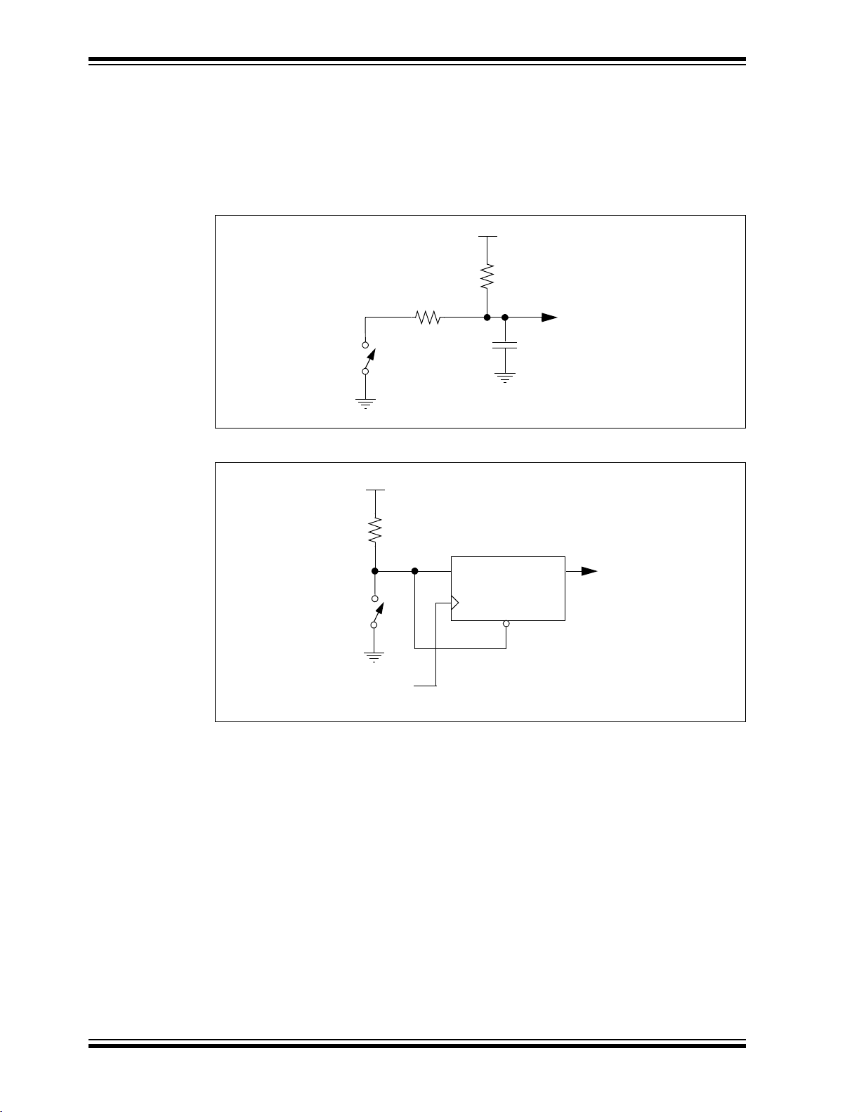
solution involved filtering, such as through a resistor-capacitor circuit, or through
re-settable shift registers (see Figure C-1 and Figure C-2). These methods are still
effective, but they involve additional cost in material, installation and board real estate.
Why suffer the additional expense when software is free and program memory is
abundant.
FIGURE C-1: FILTERING DEBOUNCE SOLUTION
+V
R2
R1
C
1
SW
Filtered
Switch
Output
FIGURE C-2: SHIFT REGISTER DEBOUNCE SOLUTION
+V
R1
Filtered
Switch
Output
SW
Debounce
Clock
D
CLK
Qn
CLR
DS40051D-page 40 2004 Microchip Technology Inc.
Page 45

C.3.1 Design
Switch bounce is intermittent contact and release of the switch contacts. Two
parameters characterize switch bounce: bounce period and bounce duration.
Bounce period is the random length of time the contacts remain open, or closed, while
the bounce is occurring. Bounce periods can vary anywhere from a few nanoseconds
to a few milliseconds.
Bounce duration is the time from the leading edge of the first bounce period to the
trailing edge of the last bounce period. The difficulty is bounce duration is
indeterminate.
Bounce abatement design starts by making assumptions based on empirical data.
The first assumption is bounce period will be absolutely less than 10 milliseconds.
Experience dictates this is a good assumption, however, bench and field-testing are still
essential to ensure the switch selected for the application does not have a longer
bounce period. The second assumption is the total bounce duration is indeterminate.
A good design should work regardless of how long the switch bounces provided that it
eventually does stop bouncing.
C.3.1.1 BRUTE FORCE DEBOUNCE
Consider a simple push button application. In this case, some event should occur when
a button is pushed. Ideally the invoked event will occur immediately, and only once for
each button push. The system should also be ready to respond to a repeat button push
as soon as possible after the button is released. This presents an apparent dilemma.
How is the difference between switch bounce and repeated button pushes determined?
Recall the assumption that the bounce period is less than 10 milliseconds. If the switch
input level is stable for longer than 10 milliseconds, then bouncing has stopped and the
input level represents the pushed or released switch state. The Brute Force method
only cares about a button-push event because this is what invokes the action. It
recognizes the switch release state as the stable state and everything else is
considered unstable. When the switch becomes unstable, the action is invoked
permitting nothing to happen until the switch returns to the released stable state.
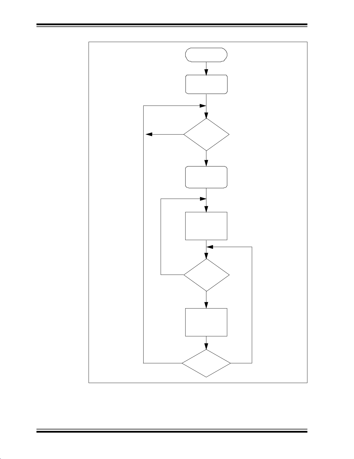
The flowchart in Figure C-3 outlines the software actions necessary to implement the
Brute Force debounce method. Notice that the debounce loop is looking for a stable
released state for 10 milliseconds before returning to the top of the main loop. Any
instability, including a stable button pushed state, resets the debounce 10 millisecond
timer.
2004 Microchip Technology Inc. DS40051D-page 41
Page 46
PICkit™ 1 Flash Starter Kit User’s Guide
FIGURE C-3: BRUTE FORCE SWITCH DEBOUNCE
Debounce
Initialize
Yes
No
Switch
Closed?
Yes
Toggle
LED
Set Timer
Count For
10 ms
Switch
Closed?
No
Decrement
Timer
Counter
Yes
DS40051D-page 42 2004 Microchip Technology Inc.
Timeout?
No
Page 47

C.3.1.2 SWITCH FILTER DEBOUNCE
There are situations when both stable switch states must be recognized. It is
undesirable for immediate action to occur if the switch intermittently leaves either the
pushed or released state. A door open or closed sensor switch is a good example of
this. If the door is closed and gets bumped, then the door-open action, such as an
alarm, should not occur because the door is still closed.
The Switch Filter Debounce method delays the response to a changed switch state.
Delay time can even be extended to several times the bounce period. Switch Filter
Debounce incorporates a saturating up/down counter. (A saturating counter is one that
stops counting when the maximum, or minimum, number is reached.) The counter
counts up when the switch is closed, and counts down when the switch is open. The
appropriate action is invoked when the counter reaches either the full up or down count.
Hysteresis is built into the count length. Switch release or contact action is invoked only
upon the first occurrence of counter saturation. The counter must saturate at the
opposite state before the previous state can be re-invoked. During switch bounce, the
counter intermittently counts up and down. The counter will progress up when the
average closed to open period favors contact, and down when the average period
favors release. The faster the switch settles in the closed or open state, the faster the
counter will reach the corresponding saturated condition.
Switch Filtering assumes, when the switch is mostly closed or open, the bouncing will
favor the closed or open levels respectively. It is possible for the counter to saturate
before the switch has stopped bouncing. It is unlikely that the counter will change
saturation state unless the count is too short, or the switch is headed in that direction.
Figure C-4 outlines the software actions necessary to implement the Switch Filtering
Debounce method.
2004 Microchip Technology Inc. DS40051D-page 43
Page 48

PICkit™ 1 Flash Starter Kit User’s Guide
FIGURE C-4: TIME AVERAGED SWITCH FILTER DEBOUNCE
Switch
Filter
No
Closed
FilterCount<
MaxCount?
Yes
Increment
FilterCount
Timer0
Overflow?
Yes
Switch
State?
Open
FilterCount>
MinCount?
Yes
Decrement
FilterCount
NoNo
No No
DS40051D-page 44 2004 Microchip Technology Inc.
FilterCount>=
MaxCount?
Yes
Turn LED1 On
Turn LED0 Off
FilterCount<=
MinCount?
Yes
Turn LED0 On
Turn LED1 Off
Page 49

C.3.2 Applications
Reliable, robust software requires debouncing of all mechanical switches. This
includes push buttons of all types, limit switches of all types and even X*Y matrix
keyboards. Matrix keyboards offer a new challenge to debouncing. Keyboards are not
a single line input level but a pattern on several inputs. One pattern represents all keys
released, or the stable state. All other patterns represent keys pressed, or the unstable
states. Reliable keyboards can be designed by debouncing to only the stable state, but
allowing new actions to occur immediately upon a change from one unstable state to
another. The solution is left to the interested student.
C.3.3
Running the Demos
There are three switch debounce demos: Debounce, SwchFltr and DbncFltr. The file
name suffix denotes the source code language for each demo. The suffix “.asm”
denotes assembly language. The suffix “.c” denotes C language. Use the Intel 32-bit
hex file output as the input file to the PICkit 1 Flash Starter Kit demo board. Intel hex
files are denoted by the “.hex” file suffix.
C.3.3.1 DEBOUNCE DEMO
Debounce is the Brute Force Debounce demo. Each button push in this demo causes
LED D0 to toggle on or off.
Perform the following steps to run the Debounce demo:
1. Connect the USB cable to the USB PC port and to the PICkit 1 Flash Starter Kit
demo board.
2. Execute the PICkit 1 Flash Starter Kit programming software.
3. From the toolbar menu, select
File -> Import Hex
. Browse to locate the hex file
named “Debounce.hex”. Select this file and click the Open button.
Note: The Program Memory window displays the program code.
4. Click the Write Device button. The status of the program write is displayed in the
status bar located at the bottom of the interface window.
5. To run the demo, push the SW1 switch on the board and observe that LED D0
toggles as expected.
C.3.3.2 SwchFltr DEMO
SwchFltr is an abbreviation for the Switch Filter Debounce demo. In this demo, LED D1
lights up when SW1 is pushed. When SW1 is released, LED D0 lights up.
Repeat steps 1 through 5 above and load the SwchFltr.hex file to run this demo.
C.3.3.3 DbncFltr DEMO
DbncFltr is an abbreviation for Debounce Filter. This demo is a combination of the
Debounce and Switch Filter demos. DbncFltr also demonstrates timed expansion of
switch functions. This demo initializes in the Switch Filter mode. Holding the button
down for more than 1 second, while in the Switch Filter mode, causes the demo to
change to the Brute Force method. LED D0 will light as an indication of the change.
Holding the button down for more than 1 second, while in the Brute Force mode,
causes the demo to change to the Switch Filter method. LED D1 will light as an
indication of the change.
Repeat steps 1 through 5 above and load the DbncFltr.hex file to run this demo.
2004 Microchip Technology Inc. DS40051D-page 45
Page 50

PICkit™ 1 Flash Starter Kit User’s Guide
C.4 LESSON 2 – INTRODUCTION TO STATE MACHINES
State Machines are an integral part of software programming. State machines make
code more efficient, easier to debug and help organize the program flow. State
machines are not limited to just firmware, they can be used to streamline any system.
However, this document limits the scope of state machines to microcontroller firmware.
C.4.1
C.4.1.1 WHAT IS A STATE MACHINE
A Finite State Machine (FSM) is based on the idea of there being finite number of states
for a given system. For instance, when an application turns an LED on and off, two
states exist; one state is when the LED is on and the other is when it is off. The example
firmware that this document refers to turns on eight LEDs sequentially. Only one LED
is on at a time, therefore eight states exist. Each state consists of one LED being turned
on while all the rest are off.
State machines require a State Variable (SV). The SV is essentially a pointer that keeps
track of the state that the microcontroller is in, and directs the program flow to the
corresponding software module. The SV can be modified in the software modules (or
states) themselves or by an outside function. The example firmware uses an outside
function which detects a button press to advance through the states.
C.4.1.2 BENEFITS OF STATE MACHINES
The introduction briefly mentioned some advantages of state machines. These advan-
tages are worth studying in greater detail because they are what make programming
with state machines so rewarding and beneficial to firmware developers.
The first advantage is using state machines inherently promotes good firmware design
techniques. When beginning to implement an application, think about what states are
necessary to make the application work. List all the pieces, or states, of an application
and then explore how they tie to one another. This will help prevent developing bugs in
the code. This line of thinking also leads to the development of a very useful engineering tool – the flow chart. The following paragraph covers state machine development in
greater detail.
State machines have one characteristic that cause them to be very beneficial. They
always return to one spot (or jump station) in the code at which the program flow is
channeled, by the state variable, to the corresponding software module. This provides
several advantages. First, this characteristic makes calling repetitive tasks on a regular
basis quite simple. Clearing the watchdog timer, checking for I/O button presses or
communicating with a host that requires periodic communication are examples of
repetitive tasks. The alternative to using state machines is to use looping code. In order
for looping code to handle repetitive tasks, the functions that handle these tasks must
be distributed throughout the code in each of the loops. This is not only highly inefficient
but also confusing to understand. Figure C-5 shows a block diagram of what the
example code would look like if a state machine where not used. Compared to
Figure C-6, which shows a block diagram of state machine based code, it is clear that
using a state machine cuts down on code space and the likelihood of missing a
repetitive task call.
Design
DS40051D-page 46 2004 Microchip Technology Inc.
Page 51

FIGURE C-5: STATE MACHINE NOT USED
Initialize Routine
Clear WDT
No
ButtonPress()?
Clear WDT
No
ButtonPress()?
Clear WDT
No
ButtonPress()?
Clear WDT
Yes
Yes
Yes
Turn only
LED0 on
Turn only
LED1 on
Turn only
LED2 on
Clear WDT
No
ButtonPress()?
Clear WDT
No
ButtonPress()?
Clear WDT
No
ButtonPress()?
Clear WDT
Yes
Yes
Yes
Turn only
LED4 on
Turn only
LED5 on
Turn only
LED6 on
No
ButtonPress()?
Yes
Turn only
LED3 on
No
ButtonPress()?
Yes
Turn only
LED7 on
2004 Microchip Technology Inc. DS40051D-page 47
Page 52

PICkit™ 1 Flash Starter Kit User’s Guide
FIGURE C-6: STATE MACHINE BASED CODE
Initialize Routine
Clear WDT
01 2
Turn only
LED0 on
Turn only
LED1 on
Turn only
LED2 on
No
ButtonPress()?
3
Turn only
LED3 on
Yes
Increment
State Variable
State Variable
=
4
Turn only
LED4 on
(1)
5
Turn only
LED5 on
6 7
Turn only
LED6 on
Turn only
LED7 on
Note 1: ButtonPress() detects when Switch 1 is pressed. This function also implements a
debounce routine not shown. See
C.4.2 “Implementation”, for details.
DS40051D-page 48 2004 Microchip Technology Inc.
Page 53

The fact that the state machine based firmware always returns to the same point in the
code also makes the firmware easier to debug. When a bug is encountered, set a break
point at the jump station. Then, step through the program state by state until the bug is
found. An example of a bug would be the SV being modified incorrectly in one of the
states. If this happens, the wrong state will be called the next time the program flow
returns to the jump station. However, because the SV is being monitored, it will be very
easy to see when an unintentional change is made to the SV and in which state the SV
was incorrectly modified.
Note: MPLAB IDE contains a built-in simulator. See the
Start Guide
available on the MPLAB IDE CD-ROM included with the
MPLAB IDE v6.xx Quick
PICkit 1 Flash Starter Kit
Another benefit of state machines is that it naturally promotes modular code. Modular
code has its own list of benefits:
1. Upgrades and special features can be easily added to the code in later revisions
or as a product evolves.
2. Modules can be cut and pasted into other applications quickly and easily.
3. Other developers will be able to understand the code in order to support it. The
jump station, if commented well, can be an index to each of the software
modules.
C.4.2
Implementation
C.4.2.1 GENERAL THOUGHT PROCESS
When implementing a FSM, first brainstorm all the states needed to complete a partic-
ular application. Once this is done, identify the first state. Next, the following question
should be answered: “What needs to happen to exit this state, and what state will it exit
to?” Usually there is more than one answer to this question. Depending on what happens while in a particular state, the state machine may advance a state, decrement a
state or skip several states entirely. As mentioned before, it is generally a good idea to
visually construct the state machine in the form of a flowchart. Finally, create a software
module for each of the states and tie them together according to the flowchart just
created.
2004 Microchip Technology Inc. DS40051D-page 49
Page 54

PICkit™ 1 Flash Starter Kit User’s Guide
C.4.2.2 TRANSLATING STATE MACHINES INTO ASSEMBLY AND C
Implementing a state machine in C is quite simple to visualize. C based state machines
rely on the “switch” statement. The following example code shows a “switch” statement
being used as a state machine.
EXAMPLE C-1: SWITCH STATEMENT
switch (STATE) {
case (State0):
// turn LED0 on
break;
case (State1):
// turn LED1 on
break;
case (State2);
// turn LED2 on
break;
... and so on
default:
STATE = State0 // if for some reason a undefined
state occurs,
// re-initialize the state machine
}
Creating a state machine in assembly is a little more difficult. In assembly, the program
flow is directed to the appropriate software module for a given state by incrementing
the Program Counter by the state variable. Incrementing the Program Counter is
comprised of incrementing PCL and PCLATH (when PCL overflows.) If a provision of
increment PCLATH is not included, then there is a risk of jumping to the wrong spot in
the program if PCL overflows. Immediately following the increment routine is a list of
“goto” statements that direct the program flow to one of the states. This method is
called a “computed goto”. The following example code shows how to use a computed
goto for a state machine.
DS40051D-page 50 2004 Microchip Technology Inc.
Page 55

EXAMPLE C-2: COMPUTED GOTO
Initialize
clrf STATE ;initialize state machine
. . .
Main
call StateMachine
. . .
goto Main
StateMachine
movlw high StateTable ;set high order byte of program
movwf PCLATH ; counter appropriately
movf STATE, W ;mask state variable to keep
andlw 03h ; things under control
addlw low StateTable ;add state variable to ROM address
btfsc STATUS C ; beginning State Table
incf PCLATH, F ;overflows? yes, increment PCLATH
movwf PCL ;move computed goto value into PC
StateTable
goto State0
goto State1
goto State2
goto State3
State0
. . .
incf STATE, F ;goto the next state
return
State1
. . .
return
2004 Microchip Technology Inc. DS40051D-page 51
Page 56

PICkit™ 1 Flash Starter Kit User’s Guide
C.4.3 Implementing this Demo
The flowchart for this demo is shown in Figure C-6, however, the flowchart does not
show the debounce routine implemented in ButtonPress(). The debounce routine
is based on the Brute Force Debounce (described in Lesson 1, Section C.3) with one
slight modification, the debounce routine is implemented as a state machine. The
Debounce state machine differs from the LED state machine where the states themselves modify the state variable. Implementing the debounce routine as a state
machine is easier to understand than implementing it as looping code.
C.4.3.1 APPLICATIONS
As mentioned earlier in Section C.4.1.2, state machines are useful in nearly every
application. The LED library, in subsequent lessons, utilizes state machines to light the
LED similarly to the state machine implemented in this lesson. State machines are useful for bit banging any number of communication protocols, receiving RF transmissions,
controlling the speed of a motor – the list goes on and on. Understanding the states
necessary to make the application work is a good way to begin implementing an application.
C.4.3.2 RUNNING THE DEMO
1. Program the state.hex code into the PIC12F629 PIC
PICkit 1 Flash Starter Kit board and programming interface.
2. If the part is programmed successfully, the D0 LED will light up. Press the SW1
switch, located on the board, to sequence through the state machine. The D1
LED will light up, then the D2 and so on.
®
microcontroller using the
C.4.3.3 FILES REQUIRED FOR PROGRAM MODIFICATION
Assembly
• state.asm
HI-TECH C
• state.c
• state.h
DS40051D-page 52 2004 Microchip Technology Inc.
Page 57

C.5 LESSON 3 – INTERRUPTS
This program demonstrates how to use the Timer0 and pin change interrupts onboard
the PIC12F6XX. In addition, the program illustrates how the PIC12F6XX is multiplexing
the LED's fast enough to give the visual representation that the LED's are all on at the
same time when in fact the LED's are lit individually. Finally, this program uses the
interrupt on-pin change to detect and debounce a button push which changes the rate
at which the LEDs are flashed.
This lesson covers the following topics:
• How to flash LEDs on the PICkit 1 Flash Starter Kit board
• How to use Timer0 and pin change interrupts on the PIC12F6XX
• How to turn a source code file into a library file for easy reuse
• Useful applications that can use the concepts presented in this lesson
• Files needed to customize the source code for the application
C.5.1
Design
One of the challenges of using an 8-pin PIC microcontroller is having enough pins for
a robust application. The PICkit 1 Flash Starter Kit utilizes design tips and tricks to get
the most out of the 8/14-pin PIC microcontroller devices. In particular, a 12-LED array
is implemented on the PICkit 1 Flash Starter Kit by using only 4 pins. In this lesson, only
8 LED's are implemented. See Table C-1 for LED multiplexing. Also, see “TIP #2
Input/Output Multiplexing”, in the
controller”
booklet (DS44040) for more details on LED multiplexing.
“Microchip Tips 'n Tricks 8-pin Flash PIC® Micro-
TABLE C-1: LED MULTIPLEXING TRUTH TABLE
PIND0D1D2D3D4D5D6D7D8D9D10D11
GP4HILOWHILOWZZZZZZHILOW
GP5 LOW HI Z Z HI LOW Z Z HI LOW Z Z
GP2 Z Z LOW HI LOW HI HI LOW Z Z Z Z
GP1ZZZZZZLOWHILOWHILOWHI
Legend:HI => Logic 1, LOW => Logic 0 and Z => TRISIO = 1
C.5.2
Implementation
The lesson utilizes interrupts to make the LED operation transparent to the main
program. The main program writes the value 0xFF to the LEDREGISTER. This flashes
8 LEDs on the PICkit 1 Flash Starter Kit board. In order to flash 4 LEDs, for example,
write 0x0F into the LEDREGISTER. The interrupt service routine uses a Timer0
interrupt for updating the LED array. A GP3 pin change interrupt detects a button push.
The Timer0 prescaler is adjusted and changes the amount of time it takes for a Timer0
interrupt to happen. This gives the visual representation that the LEDs are all on at the
same time, or sequencing.
This lesson introduces the intlib library. The intlib library contains the core functions for
flashing the LEDs and debouncing the GP3 push button. The intlib library contains the
functions Display and Debounce. The library also contains the general purpose
register, LEDREGISTER, to flash LEDs. See Section C.9.5, “Modifying the Source
Code”, for more information on the required files needed to build this project in MPLAB
IDE. Also, see the source code files for additional comments on the implementation.
For a high-level flowchart, see Figure C-10.
2004 Microchip Technology Inc. DS40051D-page 53
Page 58

PICkit™ 1 Flash Starter Kit User’s Guide
C.5.3 Applications
This program is useful in the following applications:
1. Displaying an 8-bit value onto the LED array. See Lesson 4 on using the
Analog-to-Digital Converter for reading an analog potentiometer and displaying
its value on the LED array.
2. Detecting a button push immediately.
3. Flashing LED Patterns – See Lesson 5 and Lesson 6 for displaying different LED
patterns stored in data tables.
C.5.4
1. Program the ledint.hex code to the PIC12F6XX.
2. After the hex file is programmed to the device, the LED array displays all 8 LED's
C.5.5
C.5.5.1 FILES REQUIRED FOR PROGRAM MODIFICATION
Running The Demo
that appear to be on. To change the rate at which the LED's are flashed, push the
SW1 button.
Modifying The Source Code
Assembly Source Code
• ledint.asm – Main file that contains the main program and interrupt routine
• ledint.h – Header file that defines the external program variables and routines
• intlib675.o or intlib629.o – Library file that contains the Display and Debounce
routines for the PIC12F675 or PIC12F629 respectively
• 12f629.lkr or 12f675.lkr – Linker Script for PIC12F629 and PIC12F675
respectively
(Linker Script located in C:\Program Files\MPLAB IDE\MCHIP_TOOLS)
FIGURE C-7: MPLAB PROJECT SETUP – ASSEMBLY
DS40051D-page 54 2004 Microchip Technology Inc.
Page 59
C Source Code
• ledint.c – Main file that contains the main program and interrupt routine
• ledint.h – Header file
• intlib675.obj or intlib629.obj – Library file that contains the Display and Debounce
functions for the PIC12F675 or PIC12F629 respectively
FIGURE C-8: MPLAB PROJECT SETUP – C
C.5.5.2 FILES REQUIRED FOR LIBRARY MODIFICATION
Assembly Source Code
• intlib.asm – Contains core Display and Debounce routines
(When assembled, a intlib.o file will be created)
C Source Code
• intlib.c – Contains core Display and Debounce routines
(When compiled, a intlib.obj file will be created)
• intlib.h – Header file
2004 Microchip Technology Inc. DS40051D-page 55
Page 60
PICkit™ 1 Flash Starter Kit User’s Guide
FIGURE C-9: MPLAB PROJECT SETUP – LIBRARY MODIFICATIONS
FIGURE C-10: HIGH LEVEL FLOWCHART
START
Main()
Initialize
PIC12F6XX
Load
LEDREGISTER
END
Main()
Is Button
Pushed?
Yes
Change
Flashing
Yes
No
START
Isr()
Timer0
Overflow
Interrupt?
No
GP3-Pin
Change
Interrupt?
No
END
Isr()
Yes
Update
LED Array
DS40051D-page 56 2004 Microchip Technology Inc.
Page 61

C.6 LESSON 4 – ANALOG-TO-DIGITAL CONVERTERS AND COMPARATORS
This lesson is broken up into two programs which demonstrate how to use the
analog-to-digital converter, the comparator and the internal voltage reference. The first
program set is comp.asm (written in assembly) and comp.c (written in C). This program
shows the very basic implementation of using the comparator with the internal voltage
reference. The second program set is atod.asm (written in assembly) and atod.c
(written in C). This program uses the LED display library to show the value of the
analog-to-digital (A-D) converter.
C.6.1
Comparator Lesson
For this lesson, the comparator is configured as a dedicated comparator driving the
GP2 pin directly. With <CM2:CM0> = 101, the comparator has multiplexed inputs.
GP0/CIN+ is selected as the input to the V
IN- by setting CIS = 1, thus making the analog
potentiometer the one input. The internal voltage reference is used as the other input
to the comparator on V
IN+. The module compares the potentiometer voltage with the
reference, and the logic is setup (CINV = 1) such that the output is high when the input
voltage is higher than the reference. LED3 is driven directly by the comparator and is
lit when the output of the module is high. To light D3, you must configure RA4 (GPIO4)
and RA2 (GPIO2) as digital outputs via the TRIS register, RA4 is set low and RA2 is
driven directly by the comparator without additional software overhead. The remaining
I/O's are configured as high impedance inputs.
Note: The schematics, as shown in Appendix A, display the 14-pin device pinout.
This is compatible with 8-pin devices.
The internal voltage reference is essentially a variable resistor based voltage divider
between V
reference to be 0.5 V
DD and VSS. Use the low range mode (VRR = 1) and set the internal
DD by selecting <VR3:VR0> = 1100, thus CVREF = VDD*(12/24).
By stepping through the different voltage reference settings, a basic-low resolution
analog-to-digital converter can be implemented.
The comparator module has seven different modes. Three of the modes can drive an
output pin directly. The software can monitor the output directly or create an interrupt
on change. Bits CMIE and PEIE must be set to enable the comparator interrupt which
can be used to wake the device from SLEEP.
Figure C-11 shows the project setup for the assembly and C projects.
FIGURE C-11: ASSEMBLY AND C PROJECT SETUP
2004 Microchip Technology Inc. DS40051D-page 57
Page 62

PICkit™ 1 Flash Starter Kit User’s Guide
C.6.2 Analog-to-Digital Converter Lesson
This lesson uses the PIC12F675 and demonstrates an interrupt based analog-todigital conversion. TMR0 is set up with a prescaler of 4, thus creating an interrupt
roughly every 1 ms. With every TMR0 interrupt, either the LED display routine is
serviced (see Lesson 3) or the A/D routine is serviced depending on the flag that toggles with every interrupt. Noise is generated on V
Therefore, to reduce noise in the A/D process, either a new A/D conversion is done or
the display is updated, but not simultaneously. The A/D interrupt source is not used
because the service interval (2 ms) is much longer than the conversion period of 22 µs.
The A/D module requires at least 4 µs for the sample capacitor to charge between
acquisitions, but the program allows for about 2 ms. The result of the A/D is 10 bits,
even though only the eight most significant bits are displayed on the LEDs. The result
is left justified (ADFM = 0) and the most significant byte is written to the LEDREGISTER
to be displayed. The ANSEL register specifies which of the general purpose I/O pins
are to be configured as analog inputs to the A/D module. In this case, the potentiometer's output serves as the input to AN0.
Figure C-12 shows the source code files for the assembly and C projects respectively.
FIGURE C-12: ASSEMBLY AND C SOURCE CODE FILES
DD when the LEDs are updated.
DS40051D-page 58 2004 Microchip Technology Inc.
Page 63

FIGURE C-13: ANALOG-TO-DIGITAL CONVERSION
START
lsr()
Timer0
Overflow
Interrupt?
No
Toggle A/D
Service Flag
END
lsr()
Yes
Is A/D Service
Flag Set?
No
Update LEDs
Yes
Read
A/D Register
2004 Microchip Technology Inc. DS40051D-page 59
Page 64

PICkit™ 1 Flash Starter Kit User’s Guide
C.7 LESSON 5 – PROGRAM MEMORY LOOK-UP ROUTINES
There is often a need to store constants or strings in a PIC microcontroller. Storing this
information in program memory is the best solution as long as this data never needs to
change and program memory is available. Program memory is non-volatile, therefore,
it will maintain information regardless of V
This lesson demonstrates how to retrieve data from Program Memory. It covers the
following topics:
• What a program memory look-up table is
• How a program memory look-up table is implemented
• Why a program memory look-up table is useful
DD voltage levels or PIC microcontroller reset.
C.7.1
Design
Constants stored in program memory are accessed via look-up tables. A look-up table
is similar to a computed goto (see Lesson 2) only instead of a list of goto statements,
after incrementing the program counter, there is a list of retlw instructions. Each
retlw instruction is followed by one byte of the information. Example C-3 shows a
look-up table for the string “Microchip” written in assembly language.
EXAMPLE C-3: LOOK-UP TABLE WRITTEN IN ASSEMBLY
LookupProgramMemory
movlw high StartTable
movwf PCLATH
movlw low StartTable
addwf index, w
btfsc STATUS, C
incf PCLATH, f
movwf PCL
StartTable
retlw
retlw "i"
retlw "c"
retlw "r"
retlw "o"
retlw "c"
retlw "h"
retlw "i"
retlw "p"
"M"
For this lesson, constants corresponding to a sequence of LEDs are stored in a
program memory look-up table. For instance, the first constant stored is 5F. This
corresponds to the binary number “01011111”. Each bit corresponds to an LED,
therefore, LEDs D0, D1, D2, D3, D4 and D6 will be lit when this constant is accessed.
After each look-up table, the value is displayed on the LEDs in the same fashion as
discussed in Lesson 3, using the Timer0 interrupt. The appearance of more than one
LED being lit at a time is possible because the LEDs are multiplexed fast enough that
the human eye can not detect the LEDs being turned on and off. When SW1 is pressed,
an interrupt-on-change is generated to increment the lookup to the next location.
Figure C-14 shows the flowchart for this example.
DS40051D-page 60 2004 Microchip Technology Inc.
Page 65

FIGURE C-14: PROGRAM MEMORY LOOK-UP TABLE PROCESS
START
Main()
Initialize
PIC12F6XX
Load
LEDREGISTER
END
Main()
Yes
Is Button
Pushed?
Yes
Retrieve Data
from Program
memory update
LEDs
No
START
Isr()
Timer0
Overflow
Interrupt?
No
GP3-Pin
Change
Interrupt?
No
Yes
Update
LED Array
END
Isr()
C.7.2
Applications
The lookup routines presented herein are useful in applications that require the
following:
1. Retrieving calibration values.
2. Retrieving serial numbers.
3. Retrieving LED sequences.
4. Retrieving constants or strings in general that will not change over the lifetime of
the PIC microcontroller.
2004 Microchip Technology Inc. DS40051D-page 61
Page 66

PICkit™ 1 Flash Starter Kit User’s Guide
C.7.3 Running The Demo
1. Program the pglookup.hex code to the PIC microcontroller.
2. After the hex file is programmed to the device, the LED array should show the
first look-up value in the 8 LEDs. To increment to the next look-up value, press
SW1. See Table C-2.
TABLE C-2: DATA TABLE
Instruction Byte
retlw 0x5F
retlw 0x06
retlw 0x3B
retlw 0x2F
retlw 0x66
retlw 0x6D
retlw 0x7D
retlw 0x07
DS40051D-page 62 2004 Microchip Technology Inc.
Page 67

C.8 LESSON 6 – DATA EE LOOK-UP ROUTINES
C.8.1 Introduction
Lesson 5 discussed storing and retrieving constants from program memory. The benefit
of storing information in non-volatile program memory is when power is cycled to the
microcontroller, the information is not lost. However, the main disadvantage is information stored in program memory can not change. RAM, on the other hand, offers the
versatility of change, but is volatile (it is cleared when power is cycled to the
microcontroller.) Data EEPROM solves this problem by providing non-volatile
readable/writable memory. An added benefit of data EEPROM is a developer can free
up valuable RAM by using data memory to store rarely accessed variables. This lesson
covers the following topics:
• How to implement data EEPROM look-up routines
• Why data EEPROM look-up routines are useful
C.8.2
Design
The PIC12F629/675 (DS41190) and PIC16F630/676 (DS40039) data sheets provide
detailed instructions on how to access data memory. See the data sheets for timing
specifications and limitations to the data memory. The data sheets are located on this
CD and the Microchip web site (www.microchip.com).
The steps for reading the data EEPROM are as follows:
1. Write the data memory location to the EEADR register.
2. Set EEPROM control bit RD (EECON1<0>).
All data memory locations can be accessed using a single routine when an index
variable is utilized. Example C-4 shows how to use an index variable to read the data
memory.
EXAMPLE C-4: INDEX VARIABLE
LookupDEE
movf index,w ; move data memory address pointer
banksel EEADR ; to EEADR
movwf EEADR
bsf EECON1,RD ; read data
movf EEDATA,w ; return with LED sequence in w
return
As discussed in Lesson 5, the returned value corresponds to an LED sequence. This
value is displayed using the Timer0 interrupt. The LEDs are multiplexed fast enough to
appear as though more than one LED is on at the same time. When SW1 is pressed,
an interrupt-on-change is generated and the next LED sequence is read from the data
memory. Figure C-15 shows the flowchart for this lesson.
2004 Microchip Technology Inc. DS40051D-page 63
Page 68

PICkit™ 1 Flash Starter Kit User’s Guide
FIGURE C-15: DATA EE LOOK-UP ROUTINES
START
Main()
Initialize
PIC12F6XX
Load
LEDREGISTER
END
Main()
Yes
Is Button
Pushed?
Yes
Retrieve Data
from data
memory update
LEDs
No
START
Isr()
Timer0
Overflow
Interrupt?
No
GP3-Pin
Change
Interrupt?
No
Yes
Update
LED Array
END
Isr()
C.8.3
Applications
The look-up routines presented herein are useful in applications that require the
following:
1. Storing and retrieving calibration values.
2. Maintaining current identification information.
3. Data logging information.
4. In general, for any applications that require non-volatile variable memory.
DS40051D-page 64 2004 Microchip Technology Inc.
Page 69

C.8.4 Running The Demo
1. Program the dtlookup.HEX file into the PIC microcontroller.
2. After the hex file is programmed into the device, the LED array should show the
first look-up value in the 8 LEDs. To increment to the next look-up value, press
SW1. See Table C-3.
TABLE C-3: DATA TABLE
Instruction Byte
org 2100h
DE 0x5F
DE 0x06
DE 0x3B
DE 0x2F
DE 0x66
DE 0x6D
DE 0x7D
DE 0x07
2004 Microchip Technology Inc. DS40051D-page 65
Page 70

PICkit™ 1 Flash Starter Kit User’s Guide
C.9 LESSON 7 – FREQUENCY COUNTING WITH TIMER1 GATE
This program introduces the concept of auto-calibration of the PIC12F6XX internal RC
oscillator using a known reference frequency. The PIC12F6XX has an internal RC
oscillator capable of being calibrated to ±1%.
This lesson covers the following:
• How to set up and use the Timer1 gate peripheral
• How to calibrate the PIC12F6XX internal RC oscillator
• Useful applications that use the concepts presented in this lesson
• Files needed to customize source code for the application
C.9.1
This program takes advantage of the TIMER1 gate peripheral onboard the PIC12F6XX
for auto-calibration of the PIC12F6XX device. A 2.5 kHz reference signal is connected
to pin GP4/Timer1Gate input on the PIC12F6XX device.
The PIC12F6XX internal RC oscillator has the capability to run at 4 MHz ±1%.
Using Timer1Gate is advantageous because it can eliminate busy waiting on the PIC
microcontroller. Using Timer1Gate allows the hardware to manage capturing of the
reference signal low-edge pulse width, while allowing the PIC12F6XX to process other
events for a given amount of time. The time will depend on the period of the signal
being measured. In this case, there is a 2.5 kHz reference signal. This allows 400 µs
to go and process something else before we would need to read TIMER1 for a
measurement.
C.9.2
In this program, GP0 is used to output a test signal. If the PIC12F6XX internal RC
oscillator is calibrated, the test signal will be a 5 kHz square wave. In addition, the
program uses the GP3 push button input to select calibration mode. To turn on the
2.5 kHz fixed frequency source, select the box from the Board Controls area in the
PICkit 1 Flash Starter Kit control panel. See Figure C-19 through Figure C-22 for
program flowcharts.
C.9.3
This program could be useful in the following applications:
1. High volume production environment.
2. Battery applications could use on-board calibration to recalibrate the internal RC
3. Applications that are exposed to varying voltage and temperature ranges could
Design
Implementation
Applications
oscillator as the battery voltage drops.
have intelligent on-board recalibration.
DS40051D-page 66 2004 Microchip Technology Inc.
Page 71

C.9.4 Running The Demo
1. Program the autocal.hex code to the PIC12F6XX PIC microcontroller.
2. Once the device is programmed, LED D6 turns on indicating test mode.
3. Check the device calibration by connecting an oscilloscope probe or frequency
counter to GP0 and compare the measurement to 5 kHz.
4. To calibrate the device, select the 2.5 kHz Osc checkbox and turn on the 2.5 kHz
reference signal (in the Board Controls frame), as shown in Figure C-16. Press
the SW1 button on the PICkit 1 Flash Starter Kit board. LED D7 will turn on when
the button is pushed, this indicates calibration mode.
5. View the test signal output on GP0 using the oscilloscope, or frequency counter,
and compare the measurements to the previous one before performing a
calibration. The measurement will be within 1% of 5 kHz.
FIGURE C-16: PICkit 1 FLASH STARTER KIT PROGRAMMING INTERFACE
2004 Microchip Technology Inc. DS40051D-page 67
Page 72

PICkit™ 1 Flash Starter Kit User’s Guide
C.9.5 Modifying The Source Code
C.9.5.1 REQUIRED FILES FOR PROGRAM MODIFICATION
Assembly Code
• autocal.asm – This is the only file needed to build the project
FIGURE C-17: MPLAB PROJECT SETUP – ASSEMBLY
C Code
• autocal.c – This is the main file which contains the main program, interrupt routine
and functions
• autocal.h – Header File
• delay.obj – Hi-Tech PICC Lite™ supplied delay function
(Source code is located in C:\Picclite\samples\delay)
FIGURE C-18: MPLAB PROJECT SETUP – C
DS40051D-page 68 2004 Microchip Technology Inc.
Page 73

FIGURE C-19: MAIN FLOW
START
MAIN()
Retrieve Factory
Calibration Value
Is Calibrate
Pressed?
No
FIGURE C-20: TEST FLOW
START
TEST()
Has a
Calibration
Been
Performed?
No
Button
CALL
TEST()
Yes
Yes
CALIBRATE()
Update OSCCAL
Register with
EEPROM
Calibration Value
Call
Output 5 kHz 50%
Square Wave
Is Calibration
Button Pushed?
Yes
END
TEST()
2004 Microchip Technology Inc. DS40051D-page 69
No
Page 74

PICkit™ 1 Flash Starter Kit User’s Guide
FIGURE C-21: CALIBRATE FLOW
START
CALIBRATE()
Reset
Calibration Counter
Measure 200 µs
PW
Check If The Measured
PW Is Within The
Specified Tolerance
(See Figure C-22)
PW = Pulse Width
No
Decrement
Calibration Counter
Is Calibration Counter
= 0?
Yes
Update EEPROM
Flag and Calibration Value
END
CALIBRATE()
DS40051D-page 70 2004 Microchip Technology Inc.
Page 75

FIGURE C-22: CHECKPW(W) FLOW
START
CHECKPW(W)
Yes
Yes
Is The Measured PW
= 200 µs?
No
Is The Measured PW
< 200 µs
No
Is The Measured PW
Within The Tolerance?
No
Adjust OSCCAL Down
Yes
Is The Measured PW
Within The Tolerance?
No
Adjust OSCCAL Up
Yes
END
CHECKPW(W)
PW = Pulse Width
2004 Microchip Technology Inc. DS40051D-page 71
Page 76

WORLDWIDE SALES AND SERVICE
AMERICAS
Corporate Office
2355 West Chandler Blvd.
Chandler, AZ 85224-6199
Tel: 480-792-7200
Fax: 480-792-7277
Technical Support: 480-792-7627
Web Address: www.microchip.com
Atlanta
3780 Mansell Road, Suite 130
Alpharetta, GA 30022
Tel: 770-640-0034
Fax: 770-640-0307
Boston
2 Lan Drive, Suite 120
Westford, MA 01886
Tel: 978-692-3848
Fax: 978-692-3821
Chicago
333 Pierce Road, Suite 180
Itasca, IL 60143
Tel: 630-285-0071
Fax: 630-285-0075
Dallas
4570 Westgrove Drive, Suite 160
Addison, TX 75001
Tel: 972-818-7423
Fax: 972-818-2924
Detroit
Tri-Atria Office Building
32255 Northwestern Highway, Suite 190
Farmington Hills, MI 48334
Tel: 248-538-2250
Fax: 248-538-2260
Kokomo
2767 S. Albright Road
Kokomo, IN 46902
Tel: 765-864-8360
Fax: 765-864-8387
Los Angeles
18201 Von Karman, Suite 1090
Irvine, CA 92612
Tel: 949-263-1888
Fax: 949-263-1338
San Jose
1300 Terra Bella Avenue
Mountain View, CA 94043
Tel: 650-215-1444
Fax: 650-961-0286
Toronto
6285 Northam Drive, Suite 108
Mississauga, Ontario L4V 1X5, Canada
Tel: 905-673-0699
Fax: 905-673-6509
ASIA/PACIFIC
Australia
Suite 22, 41 Rawson Street
Epping 2121, NSW
Australia
Tel: 61-2-9868-6733
Fax: 61-2-9868-6755
China - Beijing
Unit 706B
Wan Tai Bei Hai Bldg.
No. 6 Chaoyangmen Bei Str.
Beijing, 100027, China
Tel: 86-10-85282100
Fax: 86-10-85282104
China - Chengdu
Rm. 2401-2402, 24th Floor,
Ming Xing Financial Tower
No. 88 TIDU Street
Chengdu 610016, China
Tel: 86-28-86766200
Fax: 86-28-86766599
China - Fuzhou
Unit 28F, World Trade Plaza
No. 71 Wusi Road
Fuzhou 350001, China
Tel: 86-591-7503506
Fax: 86-591-7503521
China - Hong Kong SAR
Unit 901-6, Tower 2, Metroplaza
223 Hing Fong Road
Kwai Fong, N.T., Hong Kong
Tel: 852-2401-1200
Fax: 852-2401-3431
China - Shanghai
Room 701, Bldg. B
Far East International Plaza
No. 317 Xian Xia Road
Shanghai, 200051
Tel: 86-21-6275-5700
Fax: 86-21-6275-5060
China - Shenzhen
Rm. 1812, 18/F, Building A, United Plaza
No. 5022 Binhe Road, Futian District
Shenzhen 518033, China
Tel: 86-755-82901380
Fax: 86-755-8295-1393
China - Shunde
Room 401, Hongjian Building, No. 2
Fengxiangnan Road, Ronggui Town, Shunde
District, Foshan City, Guangdong 528303, China
Tel: 86-757-28395507 Fax: 86-757-28395571
China - Qingdao
Rm. B505A, Fullhope Plaza,
No. 12 Hong Kong Central Rd.
Qingdao 266071, China
Tel: 86-532-5027355 Fax: 86-532-5027205
India
Divyasree Chambers
1 Floor, Wing A (A3/A4)
No. 11, O’Shaugnessey Road
Bangalore, 560 025, India
Tel: 91-80-22290061 Fax: 91-80-22290062
Japan
Benex S-1 6F
3-18-20, Shinyokohama
Kohoku-Ku, Yokohama-shi
Kanagawa, 222-0033, Japan
Tel: 81-45-471- 6166 Fax: 81-45-471-6122
Korea
168-1, Youngbo Bldg. 3 Floor
Samsung-Dong, Kangnam-Ku
Seoul, Korea 135-882
Tel: 82-2-554-7200 Fax: 82-2-558-5932 or
82-2-558-5934
Singapore
200 Middle Road
#07-02 Prime Centre
Singapore, 188980
Tel: 65-6334-8870 Fax: 65-6334-8850
Tai wan
Kaohsiung Branch
30F - 1 No. 8
Min Chuan 2nd Road
Kaohsiung 806, Taiwan
Tel: 886-7-536-4818
Fax: 886-7-536-4803
Tai wan
Taiwan Branch
11F-3, No. 207
Tung Hua North Road
Taipei, 105, Taiwan
Tel: 886-2-2717-7175 Fax: 886-2-2545-0139
EUROPE
Austria
Durisolstrasse 2
A-4600 Wels
Austria
Tel: 43-7242-2244-399
Fax: 43-7242-2244-393
Denmark
Regus Business Centre
Lautrup hoj 1-3
Ballerup DK-2750 Denmark
Tel: 45-4420-9895 Fax: 45-4420-9910
France
Parc d’Activite du Moulin de Massy
43 Rue du Saule Trapu
Batiment A - ler Etage
91300 Massy, France
Tel: 33-1-69-53-63-20
Fax: 33-1-69-30-90-79
Germany
Steinheilstrasse 10
D-85737 Ismaning, Germany
Tel: 49-89-627-144-0
Fax: 49-89-627-144-44
Italy
Via Quasimodo, 12
20025 Legnano (MI)
Milan, Italy
Tel: 39-0331-742611
Fax: 39-0331-466781
Netherlands
Waegenburghtplein 4
NL-5152 JR, Drunen, Netherlands
Tel: 31-416-690399
Fax: 31-416-690340
United Kingdom
505 Eskdale Road
Winnersh Triangle
Wokingham
Berkshire, England RG41 5TU
Tel: 44-118-921-5869
Fax: 44-118-921-5820
05/28/04
DS40051D-page 72 2004 Microchip Technology Inc.
 Loading...