

Page 1

PICDEM™ Lab
Development Board
User’s Guide
© 2009 Microchip Technology Inc. DS41369A
Page 2

Note the following details of the code protection feature on Microchip devices:
• Microchip products meet the specification contained in their particular Microchip Data Sheet.
• Microchip believes that its family of products is one of the most secure families of its kind on the market today, when used in the
intended manner and under normal conditions.
• There are dishonest and possibly illegal methods used to breach the code protection feature. All of these methods, to our
knowledge, require using the Microchip products in a manner outside the operating specifications contained in Microchip’s Data
Sheets. Most likely, the person doing so is engaged in theft of intellectual property.
• Microchip is willing to work with the customer who is concerned about the integrity of their code.
• Neither Microchip nor any other semiconductor manufacturer can guarantee the security of their code. Code protection does not
mean that we are guaranteeing the product as “unbreakable.”
Code protection is constantly evolving. We at Microchip are committed to continuously improving the code protection features of our
products. Attempts to break Microchip’s code protection feature may be a violation of the Digital Millennium Copyright Act. If such acts
allow unauthorized access to your software or other copyrighted work, you may have a right to sue for relief under that Act.
Information contained in this publication regarding device
applications and the like is provided only for your convenience
and may be superseded by updates. It is your responsibility to
ensure that your application meets with your specifications.
MICROCHIP MAKES NO REPRESENTATIONS OR
WARRANTIES OF ANY KIND WHETHER EXPRESS OR
IMPLIED, WRITTEN OR ORAL, STATUTORY OR
OTHERWISE, RELATED TO THE INFORMATION,
INCLUDING BUT NOT LIMITED TO ITS CONDITION,
QUALITY, PERFORMANCE, MERCHANTABILITY OR
FITNESS FOR PURPOSE. Microchip disclaims all liability
arising from this information and its use. Use of Microchip
devices in life support and/or safety applications is entirely at
the buyer’s risk, and the buyer agrees to defend, indemnify and
hold harmless Microchip from any and all damages, claims,
suits, or expenses resulting from such use. No licenses are
conveyed, implicitly or otherwise, under any Microchip
intellectual property rights.
Trademarks
The Microchip name and logo, the Microchip logo, Accuron,
dsPIC, K
EELOQ, KEELOQ logo, MPLAB, PIC, PICmicro,
PICSTART, rfPIC, SmartShunt and UNI/O are registered
trademarks of Microchip Technology Incorporated in the
U.S.A. and other countries.
FilterLab, Linear Active Thermistor, MXDEV, MXLAB,
SEEVAL, SmartSensor and The Embedded Control Solutions
Company are registered trademarks of Microchip Technology
Incorporated in the U.S.A.
Analog-for-the-Digital Age, Application Maestro, CodeGuard,
dsPICDEM, dsPICDEM.net, dsPICworks, dsSPEAK, ECAN,
ECONOMONITOR, FanSense, In-Circuit Serial
Programming, ICSP, ICEPIC, Mindi, MiWi, MPASM, MPLAB
Certified logo, MPLIB, MPLINK, mTouch, PICkit, PICDEM,
PICDEM.net, PICtail, PIC
32
logo, PowerCal, PowerInfo,
PowerMate, PowerTool, REAL ICE, rfLAB, Select Mode, Total
Endurance, WiperLock and ZENA are trademarks of
Microchip Technology Incorporated in the U.S.A. and other
countries.
SQTP is a service mark of Microchip Technology Incorporated
in the U.S.A.
All other trademarks mentioned herein are property of their
respective companies.
© 2009, Microchip Technology Incorporated, Printed in the
U.S.A., All Rights Reserved.
Printed on recycled paper.
Microchip received ISO/TS-16949:2002 certification for its worldwide
headquarters, design and wafer fabrication facilities in Chandler and
Tempe, Arizona; Gresham, Oregon and design centers in California
and India. The Company’s quality system processes and procedures
are for its PIC
devices, Serial EEPROMs, microperipherals, nonvolatile memory and
analog products. In addition, Microchip’s quality system for the design
and manufacture of development systems is ISO 9001:2000 certified.
®
MCUs and dsPIC® DSCs, KEELOQ
®
code hopping
DS41369A-page ii © 2009 Microchip Technology Inc.
Page 3

Chapter 1. Overview
1.1 Introduction ..................................................................................................... 5
1.2 Highlights ........................................................................................................ 5
1.3 PICDEM™ Lab Development Kit Contents .................................................... 5
1.4 PICDEM™ Lab Development Board Construction and Layout ...................... 6
1.5 Target Power .................................................................................................. 7
1.6 Connecting the PICkit™ 2 Programmer/Debugger ........................................ 8
1.7 Solderless Prototyping Area Strip Configuration ............................................ 9
Chapter 2. Getting Started
2.1 Introduction ................................................................................................... 11
2.2 Prerequisites ................................................................................................ 11
2.3 The Software Control Loop .......................................................................... 11
2.4 MPLAB
2.5 Installing the Included Lab Files ................................................................... 16
®
IDE Download Instructions ............................................................ 12
PICDEM™LAB DEVELOPMENT
BOARD USER’S GUIDE
Table of Contents
Chapter 3. General Purpose Input/Output Labs
3.1 Introduction ................................................................................................... 17
3.2 General Purpose Input/Output Labs ............................................................. 17
3.3 GPIO Output Labs ........................................................................................ 18
3.3.1 Reference Documentation ......................................................................... 18
3.3.2 Equipment Required for GPIO Output Labs .............................................. 18
3.3.3 PICDEM Lab Development Board Setup for GPIO Output Labs ............... 18
3.3.4 Lab 1: Light LEDs ...................................................................................... 19
3.3.5 Lab 2: Flash LEDs (Delay Loop) ............................................................... 25
3.3.6 Lab 3: Simple Delays Using Timer0 .......................................................... 29
3.3.7 Lab 4: Rotate LEDs ................................................................................... 34
3.4 GPIO Input Labs ........................................................................................... 38
3.4.1 Reference Documentation ......................................................................... 38
3.4.2 Equipment Required for GPIO Input Labs ................................................. 38
3.4.3 PICDEM Lab Development Board Setup for GPIO Input Labs ................. 38
3.4.4 Lab 5: Adding a Push Button ..................................................................... 39
3.4.5 Lab 6: Push Button Interrupt ..................................................................... 48
3.4.6 Lab 7: Push Button Interrupt-on-Change .................................................. 53
3.4.7 Lab 8: Using Weak Pull-Ups ..................................................................... 58
© 2009 Microchip Technology Inc. DS41369A-page iii
Page 4

PICDEM™Lab Development Board User’s Guide
Chapter 4. Comparator Peripheral Labs
4.1 Introduction ................................................................................................... 61
4.2 Comparator Labs .......................................................................................... 61
4.2.1 Reference Documentation .........................................................................61
4.2.2 Comparator Labs .......................................................................................61
4.2.3 Equipment Required ..................................................................................61
4.2.4 Lab 1: Simple Compare .............................................................................62
4.2.5 Lab 2: Using the Comparator Voltage Reference ......................................64
4.2.6 Lab 3: Higher Resolution Sensor Readings Using a Single Comparator ...68
Chapter 5. Analog-to-Digital Converter Peripheral Labs
5.1 Introduction ................................................................................................... 75
5.2 ADC Labs ..................................................................................................... 75
5.2.1 Reference Documentation .........................................................................75
5.2.2 Equipment Required ..................................................................................75
5.2.3 Lab 1: Simple ADC ....................................................................................76
5.2.4 Lab 2: Audible Temperature Sensor ..........................................................85
Appendix A. Schematic
A.1 PICDEM Lab Development Kit Schematic ................................................... 91
DS41369A-page iv © 2009 Microchip Technology Inc.
Page 5

PICDEMTM LAB DEVELOPMENT
BOARD USER’S GUIDE
Preface
NOTICE TO CUSTOMERS
All documentation becomes dated, and this manual is no exception. Microchip tools and
documentation are constantly evolving to meet customer needs, so some actual dialogs
and/or tool descriptions may differ from those in this document. Please refer to our web site
(www.microchip.com) to obtain the latest documentation available.
Documents are identified with a “DS” number. This number is located on the bottom of each
page, in front of the p age number. The numbering convention for the DS number is
“DSXXXXXA”, where “XXXXX” is the document number and “A” is the revision level of the
document.
For the most up-to-date information on development tools, see the MPLAB
Select the Help menu, and then Topics to open a list of available on-line help files.
INTRODUCTION
®
IDE on-line help.
This chapter contains general information that will be useful to know before using the
PICDEM
• Document Layout
• Conventions Used in this Guide
• Recommended Reading
• The Microchip Web Site
• Customer Support
• Document Revision History
DOCUMENT LAYOUT
This document describes how to use the PICDEM TMLab Development Board as a
development tool to emulate and debug firmware on a target board. The manual layout
is as follows:
• Chapter 1. “Overview ”
• Chapter 2. “Getti ng Started”
• Chapter 3. “Gener al Purpo se Inp ut/Ou tp ut Lab s”
• Chapter 4. “Comparator Periphera l Labs”
• Chapter 5. “Analog- to -Di gital Converter Peri phe ral Labs”
• Appendix A. “Schematic”
TM
Lab Development Board. Items discussed in this chapter include:
© 2009 Microchip Technology Inc. DS41369A-page 1
Page 6

PICDEMTM Lab Development Board User’s Gu ide
CONVENTIONS USED IN THIS GUIDE
This manual uses the following documentation conventions:
DOCUMENTATION CONVENTIONS
Description Represents Examples
Arial font:
Italic characters Referenced books MPLAB
Emphasized text ...is the only compiler...
Initial caps A window the Output window
A dialog the Settings dialog
A menu selection select Enable Programmer
Quotes A field name in a window or
dialog
Underlined, italic text with
right angle bracket
Bold characters A dialog button Click OK
N‘Rnnnn A number in verilog format,
Text in angle brackets < > A key on the keyboard Press <Enter>, <F1>
Courier New font:
Plain Courier New Sample source code #define START
Italic Courier New A variable argument file.o, where file can be
Square brackets [ ] Optional arguments mcc18 [options] file
Curly brackets and pipe
character: { | }
Ellipses... Replaces repeated text var_name [,
A menu path File>Save
A tab Click the Power tab
where N is the total number of
digits, R is the radix and n is a
digit.
Filenames autoexec.bat
File paths c:\mcc18\h
Keywords _asm, _endasm, static
Command-line options -Opa+, -Opa-
Bit values 0, 1
Constants 0xFF, ‘A’
Choice of mutually exclusive
arguments; an OR selection
Represents code supplied by
user
“Save project before build”
4‘b0010, 2‘hF1
any valid filename
[options]
errorlevel {0|1}
var_name...]
void main (void)
{ ...
}
®
IDE User’s Guide
DS41369A-page 2 © 2009 Microchip Technology Inc.
Page 7

RECOMMENDED READING
This user’s guide describes how to use the PICDEM™ Lab Development Kit. Other
useful documents are listed below. The following Microchip documents are available
and recommended as supplemental reference resources.
Readme Files
For the latest information on using other tools, read the tool-specific Readme files in
the Readmes subdirectory of the MPLAB
contain update information and known issues that may not be included in this user’s
guide.
THE MICROCHIP WEB SITE
Microchip provides online support via our web site at www.microchip.com. This web
site is used as a means to make files and information easily available to customers.
Accessible by using your favorite Internet browser, the web site contains the following
information:
• Product Support – Data sheets and errata, application notes and sample
programs, design resources, user’s guides and hardware support documents,
latest software releases and archived software
• General Technical Support – Frequently Asked Questions (FAQs), technical
support requests, online discussion groups, Microchip consultant program
member listing
• Business of Microchip – Product selector and ordering guides, latest Microchip
press releases, listing of seminars and events, listings of Microchip sales offices,
distributors and factory representatives
Preface
®
IDE installation directory. The Readme files
© 2009 Microchip Technology Inc. DS41369A-page 3
Page 8

PICDEMTM Lab Development Board User’s Gu ide
CUSTOMER SUPPORT
Users of Microchip products can receive assistance through several channels:
• Distributor or Representative
• Local Sales Office
• Field Application Engineer (FAE)
• Technical Support
Customers should contact their distributor, representative or field application engineer
(FAE) for support. Local sales offices are also available to help customers. A listing of
sales offices and locations is included in the back of this document.
Technical support is available through the web site at: http://support.microchip.com
DOCUMENT REVISION HISTORY
Revision A (February 2009)
• Initial Release of this Document.
DS41369A-page 4 © 2009 Microchip Technology Inc.
Page 9

1.1 INTRODUCTION
The PICDEM Lab Development Board supports Microchip’s 8, 14, 18 and 20-pin 8-bit
MCUs including accommodation for PIC10F products in the 8-pin PDIP package.
Dual-row expansion headers on either side of each socket provide connectivity to all
pins on the connected PIC
explore a relatively large number of application examples without making permanent
modifications to the board. Components permanently mounted to the board are interfaced using expansion headers to the user’s application via jumper wires. A variable
supply voltage allows user’s to supply voltages between 1.2V to 5V to each of the PIC
MCU connection sockets.
1.2 HIGHLIGHTS
This chapter discusses:
• PICDEM™ Lab Development Kit Contents
• PICDEM™ Lab Development Board Construction and Layout
• Target Power
• Connecting the PICkit™ 2 Programmer/Debugger
• Solderless Prototyping Area Strip Configuration
PICDEMTM LAB DEVELOPMENT
BOARD USER’S GUIDE
Chapter 1. Overview
®
MCU. A solderless prototyping area allows the user to
1.3 PICDEM™ LAB DEVELOPMENT KIT CONTENTS
The PICDEM™ Development Kit contains the following items:
1. The PICDEM™ Lab Development Board
2. Lab component kit including:
• (1) PIC16F616 DIP
• (1) PIC12F615 DIP
• (4) 10kΩ Resistors
•(4) 1kΩ Resistors
• (8) 470Ω Resistors
• (4) 220Ω Resistors
• (4) 100Ω Resistors
• (1) 10kΩ NTC Thermistor
• (4) Green LEDs
• (4) Red LEDs
• (4) 1N4148 Diodes
•(2) 0.1μF Capacitors
•(2) 1μF Capacitors
•(2) 10μF Capacitors
• (4) Push buttons
• (10) 5” Jumper Wires
• (10) 3” Jumper Wires
© 2009 Microchip Technology Inc. DS41369A-page 5
Page 10
PICDEMTM Lab Development Board User’s Gu ide
1
2
3
4
5
6
7
8
9
10
11
12
13
14
15
16
• (10) 1” Jumper Wires
• (4) IRFD9020 P-CH MOSFETs
• (4) IRFD010 N-CH MOSFETs
• (2) 100kΩ Potentiometers
3. PICkit™ 2 Programmer/Debugger with USB Cable
4. CD-ROM including:
- “PICDEM™ Lab Development Board User’s Guide and Labs” (DS41369)
- “PIC16F631/677/685/687/689/690 Data Sheet” (DS41262)
- “Introduction to MPLAB
MCU Family Lite Mode Compiler Tutorial” (DS41322)
- Timer: Timer0 Tutorial (Part 1) (DS51682)
- Timer: Timer0 Tutorial (Part 2) (DS51702)
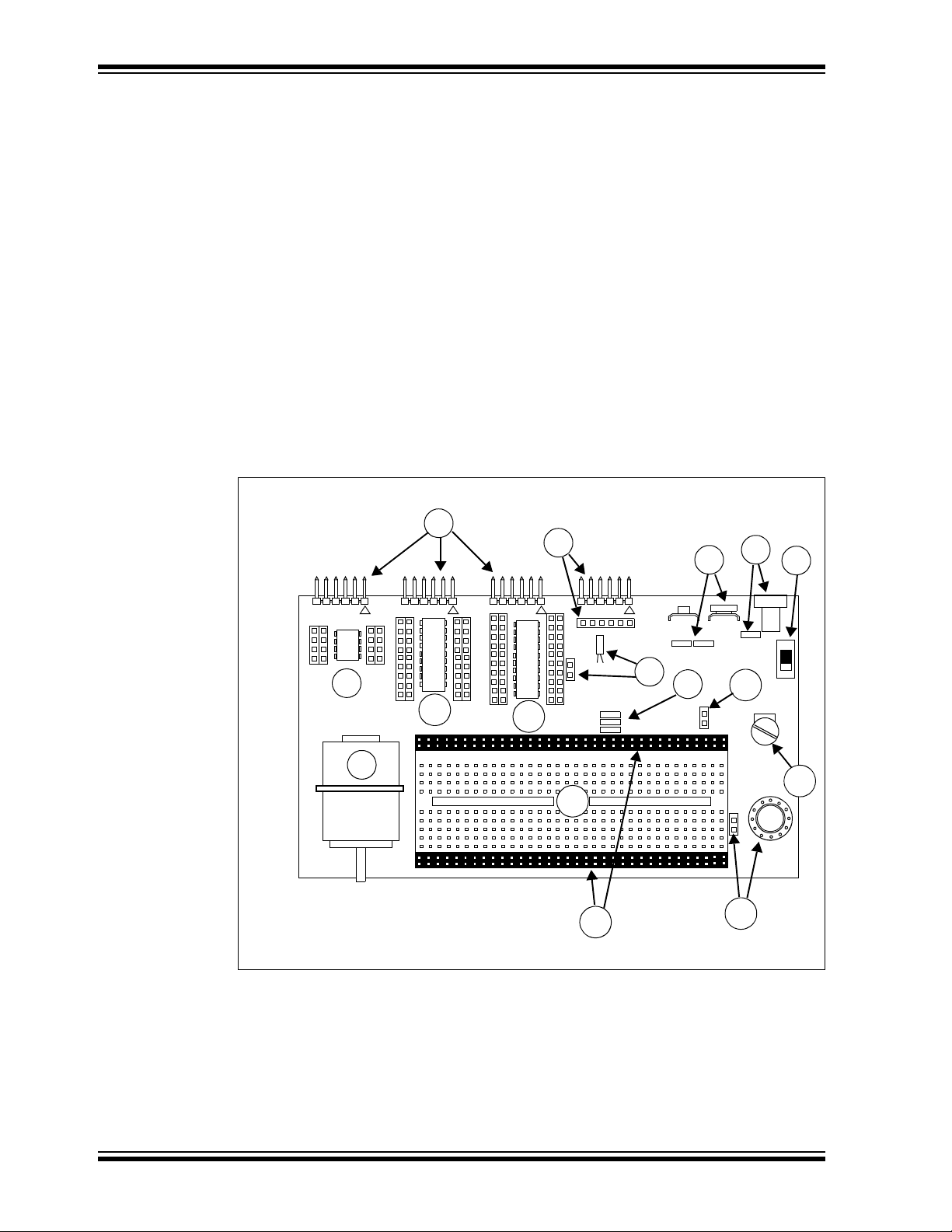
1.4 PICDEM™ LAB DEVELOPMENT BOARD CONSTRUCTION AND LAYOUT
The Low Pin Count USB Development Board and populated components are shown in
Figure 1-1.
FIGURE 1-1: PICDEM™ LAB DEVELOPMENT BOARD
®
IDE and HI-TECH C® PRO for the PIC10/12/16
DS41369A-page 6 © 2009 Microchip Technology Inc.
1. PICkit™ 2 Programmer/Debugger Connection Headers (J13, J12 and J6)
a) J13 dedicated to PIC
b) J12 dedicated to PIC
c) J6 dedicated to PIC
2. PICkit™ Serial Analyzer Connection Header (J11) and Receptacle (J15)
To use the PICkit™ Serial Analyzer, connect to appropriate PIC MCU expansion
header using jumper wires from receptacle.
®
microcontroller socket U5
®
microcontroller socket U3
®
microcontroller socket U2
Page 11

Overview
3. 32 kHz Crystal Oscillator (Y1) and Connection Header (J7)
4. V
DD Connect/Disconnect Jumpers (J3, J4, J5)
a) J3 jumper connects/disconnects V
U2
b) J4 jumper connects/disconnects V
U3
c) J5 jumper connects/disconnects V
U5
5. Battery Clip Connection (BT1) for 9V Battery and Jumpers (J14)
J14 jumpers connect/disconnect battery terminals for use in future lab on battery
chargers.
6. 9 V
DC Supply Connector (J1) and Connect/Disconnect Jumper (J2)
7. Power ON Switch (SW1)
8. 8-Pin PDIP PIC10F MCU Socket (U5) and Bilateral Dual-Row Expansion
Headers (J10 and J18)
Dual-row expansion headers provide connectivity to each pin on the PIC10F206
MCU populating socket U5.
9. 5V Brushed DC Motor
10. 18-Pin PDIP PIC MCU Socket (U3) and Bilateral Dual-Row Expansion Head-
ers (J17 and J16)
Dual-row expansion headers provide connectivity to each pin on the PIC16F819
MCU populating socket U3.
11. 8, 14, 20-Pin PDIP PIC MCU Socket (U2) and Bilateral Dual-Row Expansion
Headers (J8 and J9)
Dual-row expansion headers provide connectivity to each pin on the PIC16F690
MCU populating socket U2.
12. Solderless Prototyping Area
13. Bilateral Dual-Row Supply Headers (J22 and J23)
Provide both V
DD and VSS connectivity bilaterally to the solderless prototyping
area.
14. 0.2 Watt, 8-Ohm Speaker (LS1) with Connection Header (J19)
J19 connector used to connect speaker LS1 to user application using jumper
wires.
15. Battery Positive (CP+) and Negative (CP-) Connection Header (J26)
Provides connectivity of positive and negative battery terminals to the user application using jumper wires.
16. Variable V
DD Potentiometer (R1)
Potentiometer used to vary PIC MCU supply voltage from approximately 1.3V to
approximately 5V.
DD1 supply to PIC16F690 MCU in socket
DD2 supply to PIC16F819 MCU in socket
DD3 supply to PIC10F206 MCU in socket
1.5 TARGET POWER
The PICDEM™ Lab Development Board can be powered in one of three ways:
1. Using a 9-12 V
(MIcrochip part #AC162039 recommended)
Ensure that connect/disconnect jumper J2 is in place.
© 2009 Microchip Technology Inc. DS41369A-page 7
DC power supply connected to connector J1
Page 12

PICDEMTM Lab Development Board User’s Gu ide
2. Using a 9V battery connected to connector BT1
Ensure that connect/disconnect jumpers J14 are in place.
3. A PICkit™ 2 Programmer/Debugger connected to any one of the three PICkit™
Programmer/Debugger connectors J13, J12 and J6 (recommended for
low-power applications only).
Note: When using the PICkit™ 2 Programmer/Debugger as the power source,
the variable V
When using methods 1 or 2, each PIC
connect/disconnect jumper that, when in place, enables the positive supply voltage to
the respective V
DD pins. The VDD jumpers connect to the following PIC
troller sockets:
DD1 (J3) connects/disconnects supply voltage to the PIC
1. V
populating U2.
2. V
DD2 (J4) connects/disconnects supply voltage to the PIC
populating U3.
3. V
DD3 (J5) connects/disconnects supply voltage to the PIC
populating U5.
Using methods 1 or 2 enables the use of the variable V
supply voltages from approximately 1.3 to 5V. Rotating the potentiometer clockwise will
raise the supply voltage while rotating the potentiometer counterclockwise will
decrease the supply voltage.
DD potentiometer (R1) will not vary the supply voltage.
®
microcontroller has an associated
®
®
microcontroller
®
microcontroller
®
microcontroller
DD potentiometer (R1) to control
microcon-
1.6 CONNECTING THE PICkit™ 2 PROGRAMMER/DEBUGGER
The three PIC® microcontrollers populating sockets U5, U3 and U2 have their own
PICkit™ Programmer/Debugger (ICSP™) connectors so that each can be programmed or debugged individually. The ICSP™ connect to the following PIC
controller sockets:
1. ICSP1 (J6) connects to the PIC
2. ICSP2 (J12) connects to the PIC
3. ICSP3 (J13) connects to the PIC
The PICkit™ Programmer/Debugger connects to the ICSP™ connector as shown in
Figure 1-2.
®
microcontroller populating U2.
®
microcontroller populating U3.
®
microcontroller populating U5.
®
micro-
DS41369A-page 8 © 2009 Microchip Technology Inc.
Page 13
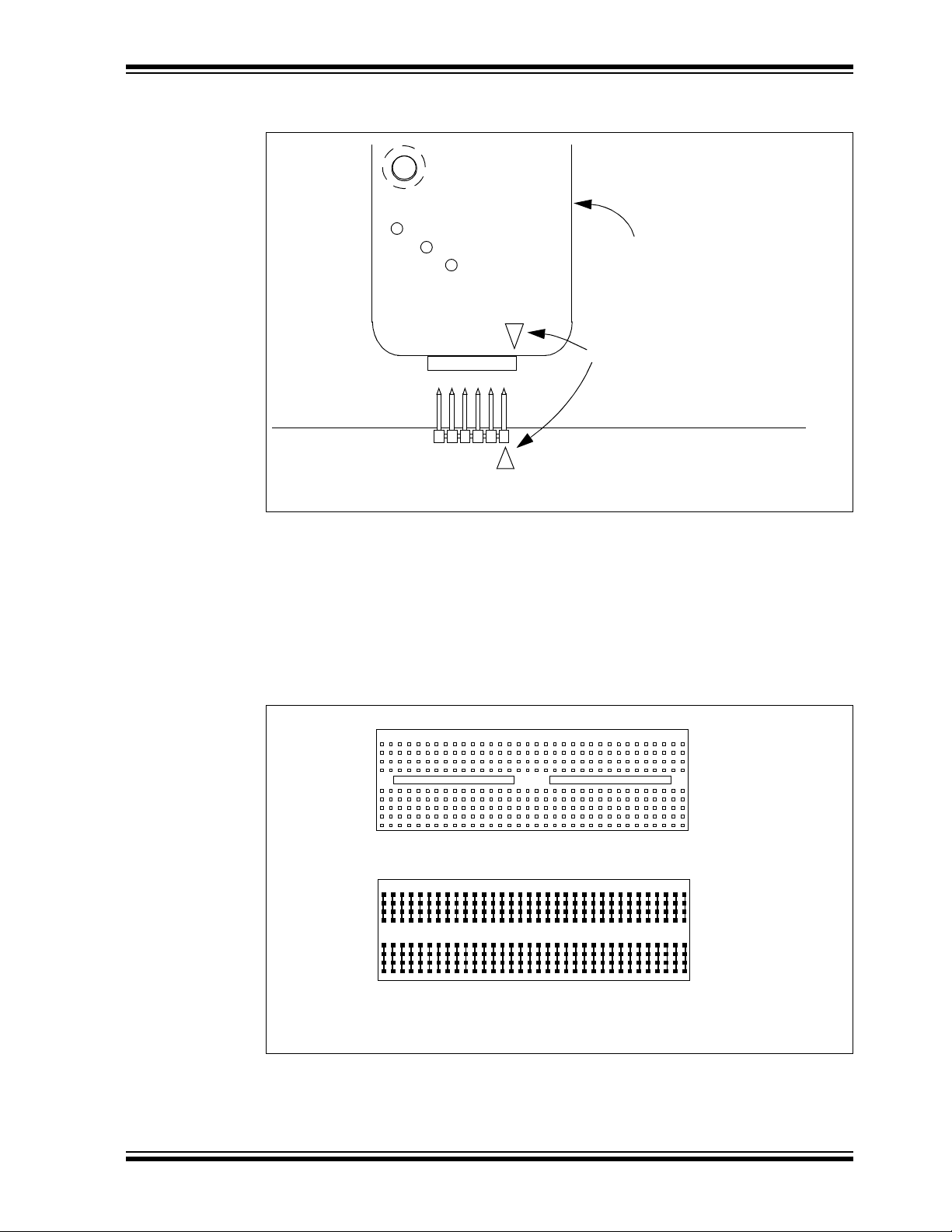
Overview
ICSP™ CONNECTOR
P
o
we
r
T
a
r
g
e
t
B
u
s
y
PICkit™ Programmer/Debugger
Denotes Pin 1
Solderless Prototyping Area
Solderless Prototyping Area
Showing Strip Connections
FIGURE 1-2: CONNECTING THE PICkit™ PROGRAMMER/DEBUGGER TO
AN ICSP™ CONNECTOR
The PICkit™ 2 Programmer/Debugger is then connected to an available USB port on
the PC using the included USB cable.
1.7 SOLDERLESS PROTOTYPING AREA STRIP CONFIGURATION
The solderless prototyping area contains a variety of strips under the perforated plastic
block. These strips “short” vertical rows of holes together as shown in Figure 1-3.
FIGURE 1-3: SOLDERLESS PROTOTYPING AREA STRIP
CONFIGURATION
© 2009 Microchip Technology Inc. DS41369A-page 9
Page 14

PICDEMTM Lab Development Board User’s Gu ide
NOTES:
DS41369A-page 10 © 2009 Microchip Technology Inc.
Page 15

PICDEMTM LAB DEVELOPMENT
main()
Loop Forever
Timing()
Initialize()
Get_Inputs()
Decide()
Do_Outputs()
Chapter 2. Getting Started
2.1 INTRODUCTION
This chapter is intended to prepare the reader to complete the labs in the remaining
chapters of this user’s guide.
2.2 PREREQUISITES
The labs contained within this lab manual assumes the user:
1. Has a basic understanding of the C programming language.
2. Understands basic circuit analysis.
3. Has completed or understands the concepts contained within the introductory
tutorial: “Introduction to MPLAB
MCU Family Lite Mode Compiler Tutorial” (DS41322B) provided on the
accompanying CD-ROM.
2.3 THE SOFTWARE CONTROL LOOP
BOARD USER ’S GUIDE
®
IDE and HI-TECH C® PRO for the PIC10/12/16
The labs used in this user’s guide implement a software control loop in various
configurations but always in the same sequence as shown in Example 2-1.
FIGURE 2-1: MAIN() SOFTWARE CONTROL LOOP FLOWCHART FOR
USED IN LABS
Each block of the software control loop represents a function that organizes tasks into
logical, organized groupings that are called from the main function (main()). Notice
© 2009 Microchip Technology Inc. SD41369A-page 11
the Initialize() is called only once while the remaining functions are executed
repeatedly. This method organizes the embedded firmware application into a logic
sequence of events:
Page 16

PICDEMTM Lab Development Board User’s Gu ide
void main(void)
{
Initialize(); //Initialize the relevant registers
while(1)
{
Decide();//Make any decisions
Do_Outputs(); //Perform any outputs
Timing();//Sets execution rate of the
//Software Control Loop
}
}
1. Initalize():
- Initializes the microcontroller, the peripherals used in the application and any
global variables used by multiple functions.
2. Get_Inputs():
- Obtains any input information either on-chip (from internal registers, etc...) or
off-chip (pin voltage levels).
3. Decide():
- Makes decisions based on the input information gathered in the previous
function to manipulate global variables.
4. Do_Outputs():
- Based on the decisions made in the previous function, this function outputs
data onto the pins of the microcontroller or to registers within the device.
5. Timing():
- This function determines how fast the software control loop executes.
Example 2-1 shows a typical main() calling the various functions that make up the
software control loop.
EXAMPLE 2-1: TYPICAL SOFTWARE CONTROL LOOP MAIN() USED IN
LABS
An infinity loop will be used by all labs in this user’s guide created using a while
loop that repeatedly call the functions within the curly braces as long as there is power
to the microcontroller.
Global variables are used wherever needed in lieu of passing variables between
functions.
2.4 MPLAB® IDE DOWNLOAD INSTRUCTIONS
SD41369A-page 12 © 2009 Microchip Technology Inc.
The following steps outline how to download the latest version of the MPLAB IDE and
HI-TECH C
mended that all open programs and applications are closed to expedite the installation
process.
®
PRO for the PIC10/12/16 MCU Families compiler. It is strongly recom-
Page 17
Getting Started
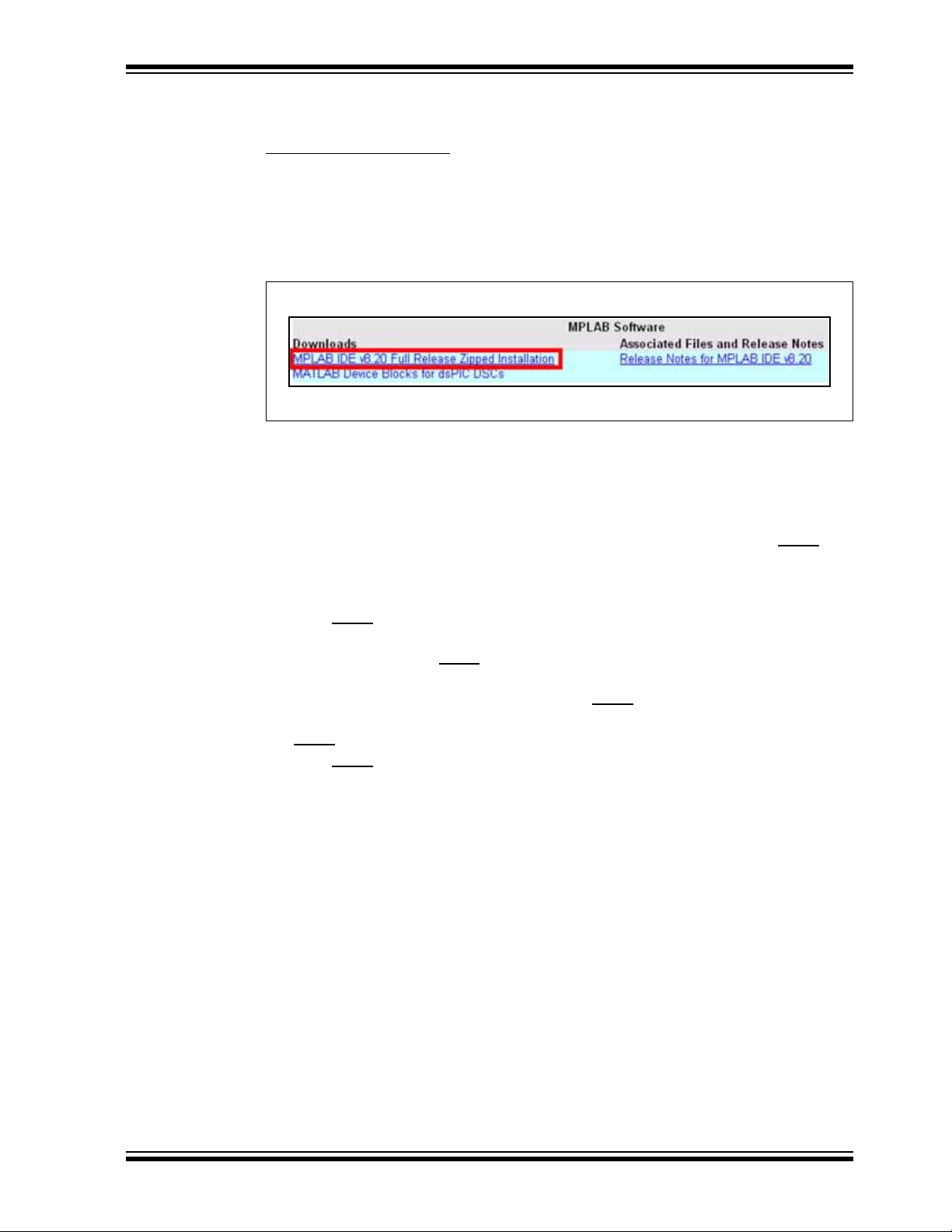
1. Using a PC that is connected to the internet, navigate to the MPLAB® IDE down-
load page at the following url:
www.microchip.com/mplab
This page outlines the MPLAB IDE and also features downloadable plug-ins, User’s
Guides and other useful information.
2. Scroll down to the Downloads section of the page and select the latest full
release zip file for MPLAB IDE vx.xx. (See Figure 2-2.)
FIGURE 2-2: MPLAB ZIP FILE
3. When prompted open the .zip file and extract all contents to a new folder named
something meaningful such as “MPLAB” created in a directory such as Desktop
or another location easily accessible.
4. Once all files are extracted, navigate to the folder created and double click on the
Install_MPLAB_vxxx.exe file to start the installation process.
5. The MPLAB
proceed with the installation.
6. In the next window, read through the MPLAB IDE License Agreement and ensure
that the I accept the terms of the license agreement radio button is selected.
Click Next>
7. In the Setup Type window select the setup type (complete is recommended for
new users) and click Next>
8. In the Choose Destination Location it is recommended to use the default direct
C:\Program Files\Microchip\. Click Next>
9. Accept the Application Maestro License agreement in the next window and click
Next>
to continue.
10. Click Next>
take several minutes to complete).
11. During the installation process, the user will be prompted to install the free
HI-TECH C
the user install the compiler at this point. Select Yes to launch the installer. In the
installer window, click Next to continue. (See Figure 2-3.)
Tools x.xx Installation window should now be open. Click Next> to
®
to continue with the installation.
to continue.
to continue.
in the Start Copying Files window to start the installation (this may
®
PRO for the PIC10/12/16 MCU Compiler. It is recommended that
© 2009 Microchip Technology Inc. SD41369A-page 13
Page 18
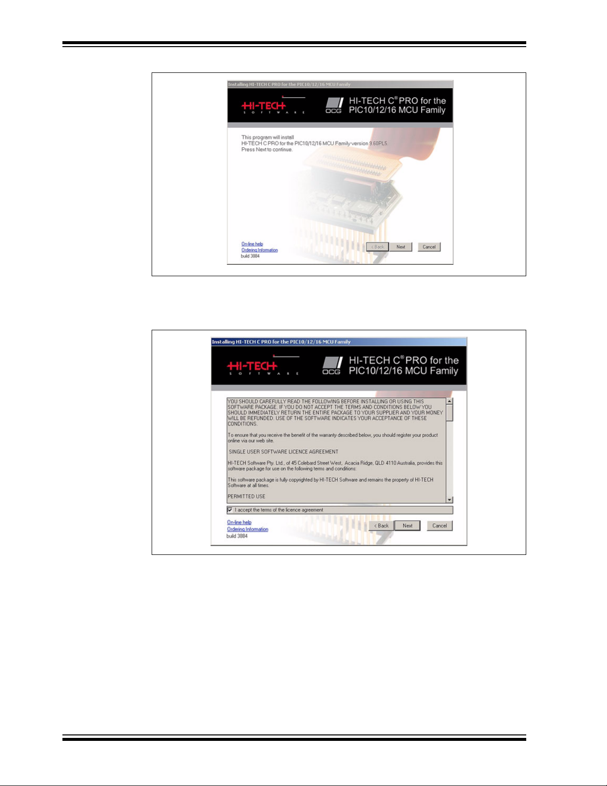
PICDEMTM Lab Development Board User’s Gu ide
FIGURE 2-3: HI TECH INSTALLER WINDOW
12. In the next window, accept the terms of the license agreement and click Next to
continue. (See Figure 2-4.)
FIGURE 2-4: HI TECH LICENSE AGREEMENT
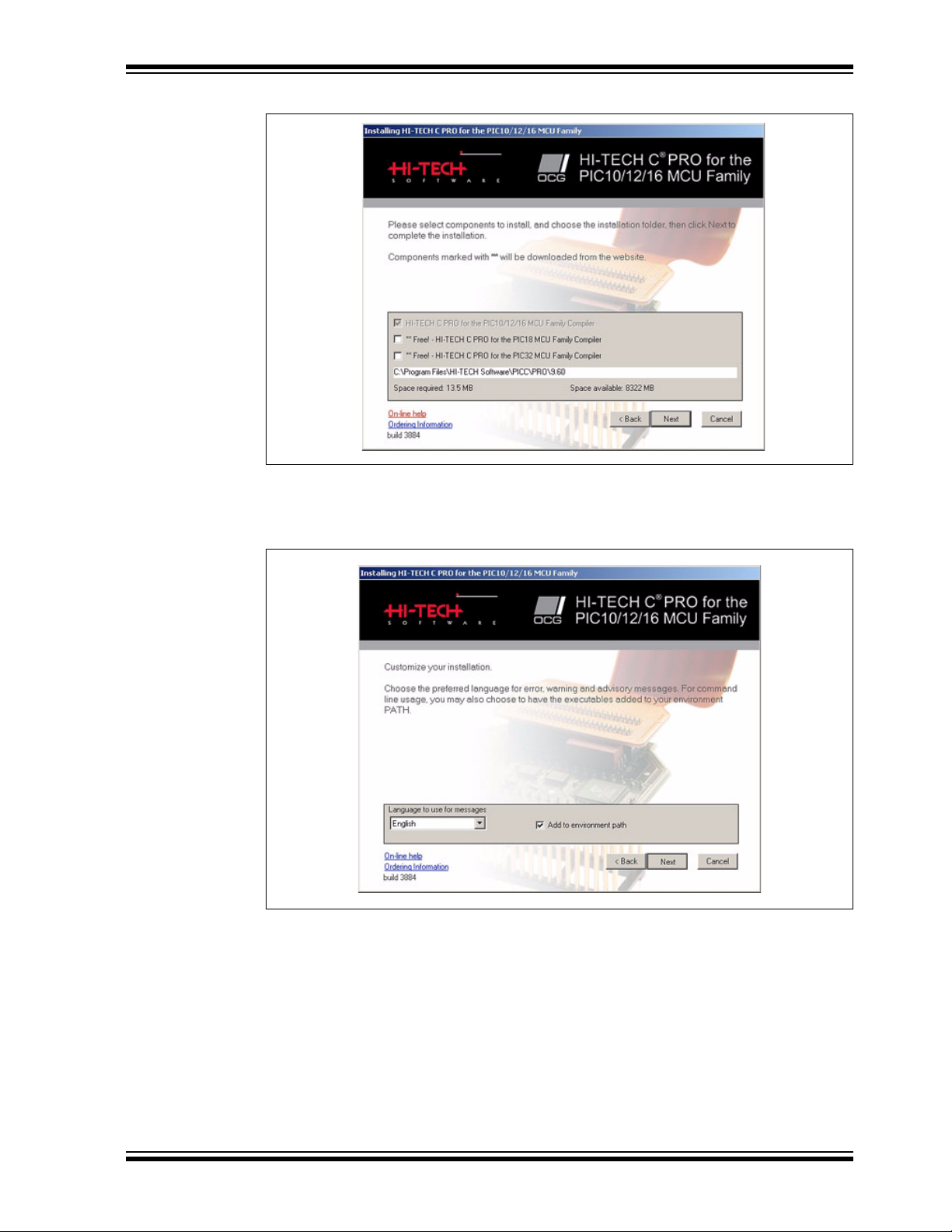
13. In the next window, select any components in addition to the HI-TECH C
the PIC10/12/16 MCU Family Compiler to install (additional components are not
required to complete the labs in this user's guide) and click Next to continue.
(See Figure 2-5.)
®
Pro for
SD41369A-page 14 © 2009 Microchip Technology Inc.
Page 19
Getting Started
FIGURE 2-5: HI TECH COMPONENTS
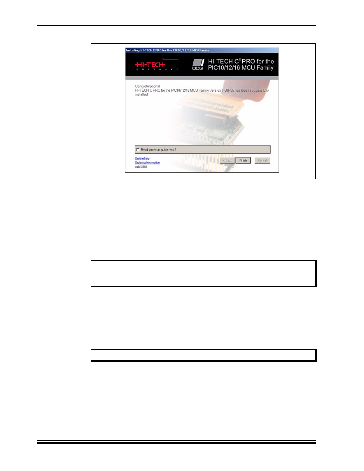
14. In the next window, choose the language of preference, select the Add to
environment path radio button and click Next to continue. (See Figure 2-6.)
FIGURE 2-6: HI TECH LANGUAGE PREFERENCES
The installation process will now begin.
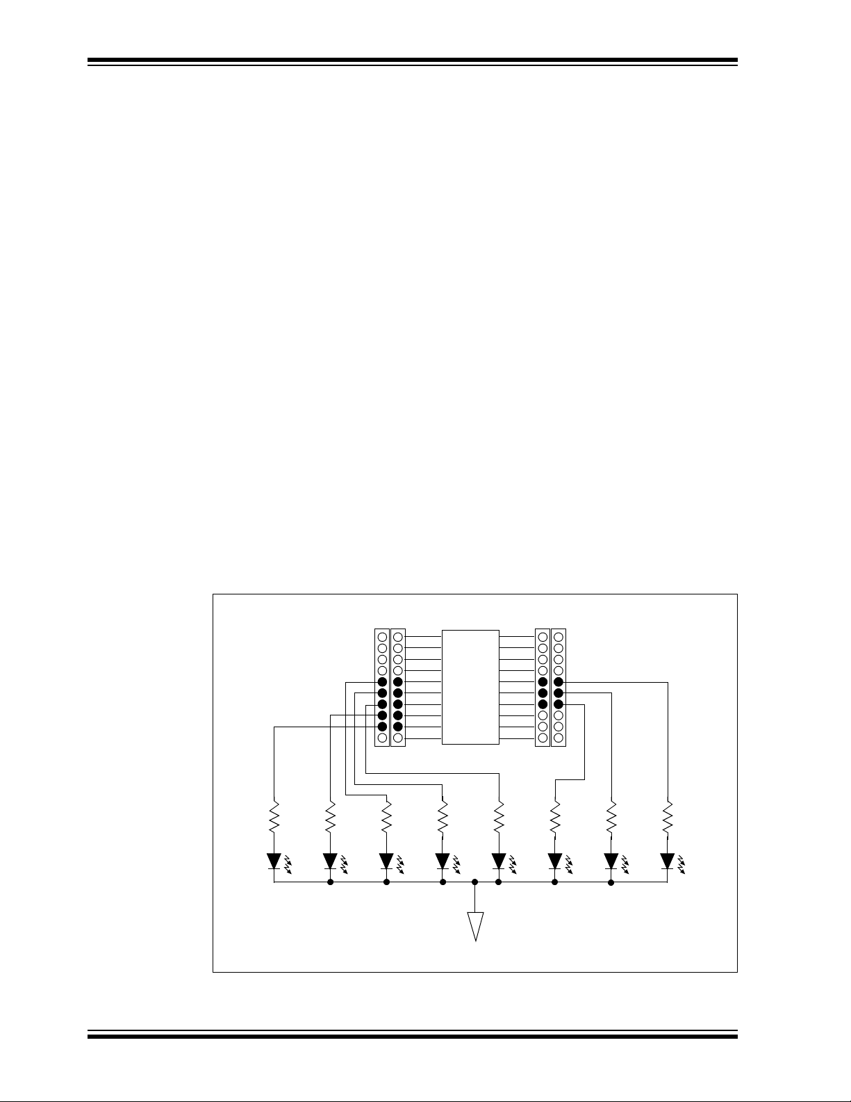
15. Once the installation is complete, a confirmation window will open. Select or
de-select the Read quick start gui de now? radio button and click Finish to
proceed. (See Figure 2-7.)
© 2009 Microchip Technology Inc. SD41369A-page 15
Page 20
PICDEMTM Lab Development Board User’s Gu ide
FIGURE 2-7: HI TECH INSTALL CONFIRMATION
16. The MPLAB
and prompt the user to restart the computer before using the software. To begin
using the tools, select the Yes, I want to restart my computer radio button and
click Finish to end the installation process and restart the computer.
Following restart, the user will be given the option to view a variety of documentation.
To view a document, simply highlight and click View Selected File.
The MPLAB
Compiler are now both installed and ready to use. The user is now ready to complete
the labs included in this user’s guide.
Note: A comprehensive introduction to the “HI-TECH C® PRO for the
®
Tools Install Shield Wizard Complete window should soon open
®
IDE and HI-TECH C® PRO for the PIC10/12/16 MCU Family Lite Mode
PIC10/12/16 MCU Family Lite Mode Compiler Tutorial” (DS41322) is
provided on the accompanying CD-ROM.
2.5 INSTALLING THE INCLUDED LAB FILES
The PICDEM™ Lab Development Kit CD-ROM includes a .zip file called
PICDEM_Lab.zip. This file provides a location for the user to save any projects
created while completing the labs in this user's guide and contains solutions for each
lab in a folder labeled solution. To install this folder, simply extract the contents of
the .zip file to the C:\ directory.
Note: Lab folders must be installed to the C:\ to be used by the MPLAB IDE.
SD41369A-page 16 © 2009 Microchip Technology Inc.
Page 21

Chapter 3. General Purpose Input/Output Labs
3.1 INTRODUCTION
The following labs cover some of the fundamental features of the General Purpose
Input/Output (GPIO) peripherals available on the PIC16F690. As the name implies,
these peripherals are used for general purpose applications that can monitor and
control other off-chip devices. Some PIC
peripherals on-chip including the PIC16F690 used in the following labs. Therefore, the
PORTx naming convention is used. Available ports on the PIC16F690 are:
•PORTA
•PORTB
•PORTC
Reading through the data sheet highlights some of the unique characteristics associated with each port and the reader is encouraged to explore these in greater detail once
comfortable with the labs in this user’s guide. The labs will focus on two of the port
peripherals: PORTC and PORTA. Labs will be naturally divided into two sections since
these are General Purpose Input/Output peripherals:
• Output Labs
• Input Labs
Output labs will introduce the reader to concepts necessary to configuring these peripherals for output to off-chip devices using applicable registers by lighting 8 LEDs connected to the PORTC pins
The Input labs will then add a push button interfacing to one of the PORTA pins to highlight concepts necessary for configuring these peripherals to receive information from
off-chip devices. Finally, interrupts will be used to optimize the application for different
purposes.
PICDEMTM LAB DEVELOPMENT
BOARD USER’S GUIDE
®
microcontrollers have multiple GPIO
3.2 GENERAL PURPOSE INPUT/OUTPUT LABS
• Output Labs:
- Lab 1: Light LEDs
- Lab 2: Flash LEDs (Delay Loop)
- Lab 3: Simple Delays Using Timer0
- Lab 4: Rotate LEDs
• Input Labs:
- Lab 5: Adding a Push Button
- Lab 6: Push Button Interrupt
- Lab 7: Push Button Interrupt-on-Change
- Lab 8: Using Weak Pull-ups
© 2009 Microchip Technology Inc. DS41369A-page 17
Page 22
PICDEMTM Lab Development Board User’s Gu ide
U2
1
2
3
4
5
6
7
8
9
10
20
19
18
17
16
15
14
13
12
11
RC0
RC1
RC2
RC3
RC4
RC5
RC6
RC7
J9J8
R8
470Ω
R4
470Ω
R7
470Ω
R6
470Ω
R5
470Ω
R3
470Ω
R2
470Ω
R1
470Ω
LED8 LED7 LED6 LED4 LED3 LED2 LED1LED5
V
SS
3.3 GPIO OUTPUT LABS
3.3.1 Reference Documentation
All documentation is available on the PICDEM™ Lab Development Kit accompanying
CD-ROM.
• PIC16F690 Data Sheet (DS41262)
- Section 2.2.2.2: Option Register
- Section 2.2.2.3: Interrupt Control Register INTCON
- Section 4: I/O Ports
- Section 5: Timer0 Module
• Timers: Timer0 Tutorial (Part 1) (DS51628)
• Timers: Timer0 Tutorial (Part 2) (DS51702)
• “Introduction to MPLAB
Family Lite Mode Compiler Tutorial” (DS41322)
3.3.2 Equipment Required for GPIO Output Labs
To complete the labs in this section, the following components are required:
1. 8 – Light Emitting Diodes
2. 8 – 470Ω resistors
3. PIC16F690 populating socket U2
4. Assorted jumper wires
®
IDE and HI-TECH C® PRO for the PIC10/12/16 MCU
3.3.3 PICDEM Lab Development Board Setup for GPIO Output Labs
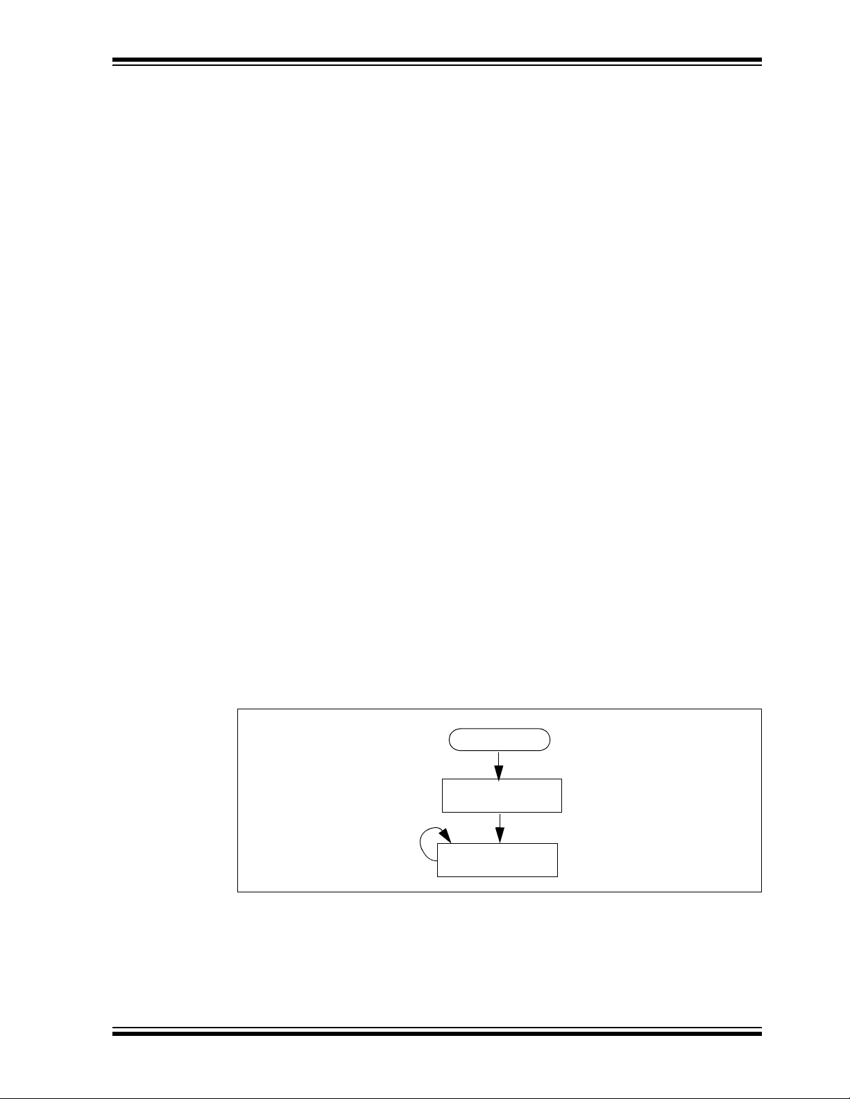
The GPIO output labs will require that the PICDEM Lab Development Board be configured as shown in Figure 3-1 using the components listed in the previous section.
FIGURE 3-1: PICDEM LAB SCHEMATIC FOR GPIO OUTPUT LABS
DS41369A-page 18 © 2009 Microchip Technology Inc.
Page 23
General Purpose Input/Output Labs
main()
Initialize()
Do_Outputs()
Loop Forever
Special care should be observed when connecting the LED jumper wires to the
expansion headers surrounding the PIC16F690, as the PORTC pins are not in
sequential order. The 470Ω resistors are used to limit the current across the LEDs to
manufacturer specifications. Furthermore, the PIC16F690 Data Sheet electrical
specifications (see Section 17.0) specify that each port pin should not source/sink more
than 25 mA. The maximum output current sourced/sunk by all port pins combined
should not exceed 200 mA. The 470Ω resistors keep all source current well within
these specifications.
3.3.4 Lab 1: Light LEDs
3.3.4.1 NEW REGISTERS USED IN THIS LAB
To configure the peripherals used in this lab, the following registers are used:
1. PORTC Register: PORTC (Register 4-11 in Section 4 of the PIC16F690 Data
Sheet).
- 8-bit bidirectional port.
2. PORTC Tri-State Register: TRISC (Register 4-12 in Section 4 of the PIC16F690
Data Sheet).
- Configures corresponding bits in PORTC as either input or output.
3. Analog Select Register High and Analog Select Register Low: ANSELH and
ANSEL (Registers 4-4 and 4-3 in Section 4 of the PIC16F690 Data Sheet).
- Configure associated pins for analog or digital input signals.
3.3.4.2 OVERVIEW
This first lab demonstrates how to output data from the PORTC peripheral on the
PIC16F690 to its associated pins. LEDs connected to PORTC pins will light when the
associated pin is driven high (approx. V
(approx. V
need to be configured as output using the TRISC register. Also, PORTC pins RC0,
RC1, RC2, RC3, RC6 and RC7 are configurable for both analog and digital signals. On
start-up, any analog/digital functional pin is defaulted to analog. Therefore, this
application will require that these pins be configured as digital by configuring the
associated bits in the ANSEL and ANSELH analog select registers.
FIGURE 3-2: MAIN() SOFTWARE CONTROL LOOP FLOWCHART FOR
SS). The port peripherals will all default to input on start-up and will therefore
LAB 1
DD) or turn the LED OFF when driven low
© 2009 Microchip Technology Inc. DS41369A-page 19
Page 24
PICDEMTM Lab Development Board User’s Gu ide
Figure 3-2 shows the software control loop that will be implemented in this lab. At
device power-up, the first functional block called from the main() is Initialize().
This function will initialize the PORTC peripheral as follows:
• Clear the PORTC register data
• Configure the ANSEL and ANSELH bits so that all associated PORTC pins are
digital
• Configure the associated PORTC pins as all output using the TRISC register
Note: The PORT register should always be initialized to a known value before
configuring the associated TRIS bit. This avoids unexpected voltage levels
on the associated pins since at start-up port bit values are unknown.
The next function called from main() is Do_Outputs(). This function will assign
values to the PORTC register that will drive the associated pins high or low to light the
LEDs connected.
3.3.4.3 PROCEDURE
The following steps will demonstrate how to create a new project in MPLAB
more in-depth tutorial is provided in the document “Introduction to MPLA B
HI-TECH C
(DS41322) included on the accompanying CD-ROM.
1. Open MPLAB IDE by selecting Start>Microchip>MPLAB IDE vX.XX>MPLAB
IDE.
2. In the MPLAB IDE toolbar, select Project>Project Wizard....
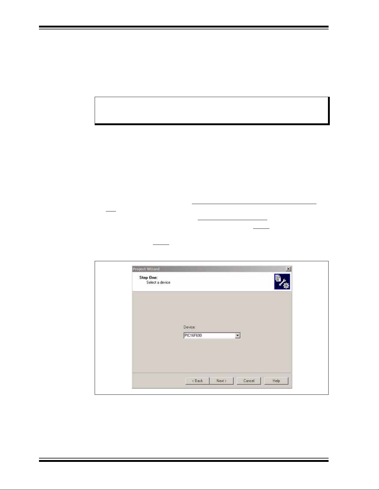
3. The Welcome dialog box should now be open. Select Next> to proceed.
4. In the Step One: window, select the PIC16F690 from the Device: drop-down
menu and select Next>
®
PRO for the PIC10/12/16 MCU Family Lite Mode Compiler Tutorial”
to continue. (See Figure 3-3.)
®
IDE. A
®
IDE and
FIGURE 3-3: STEP ONE
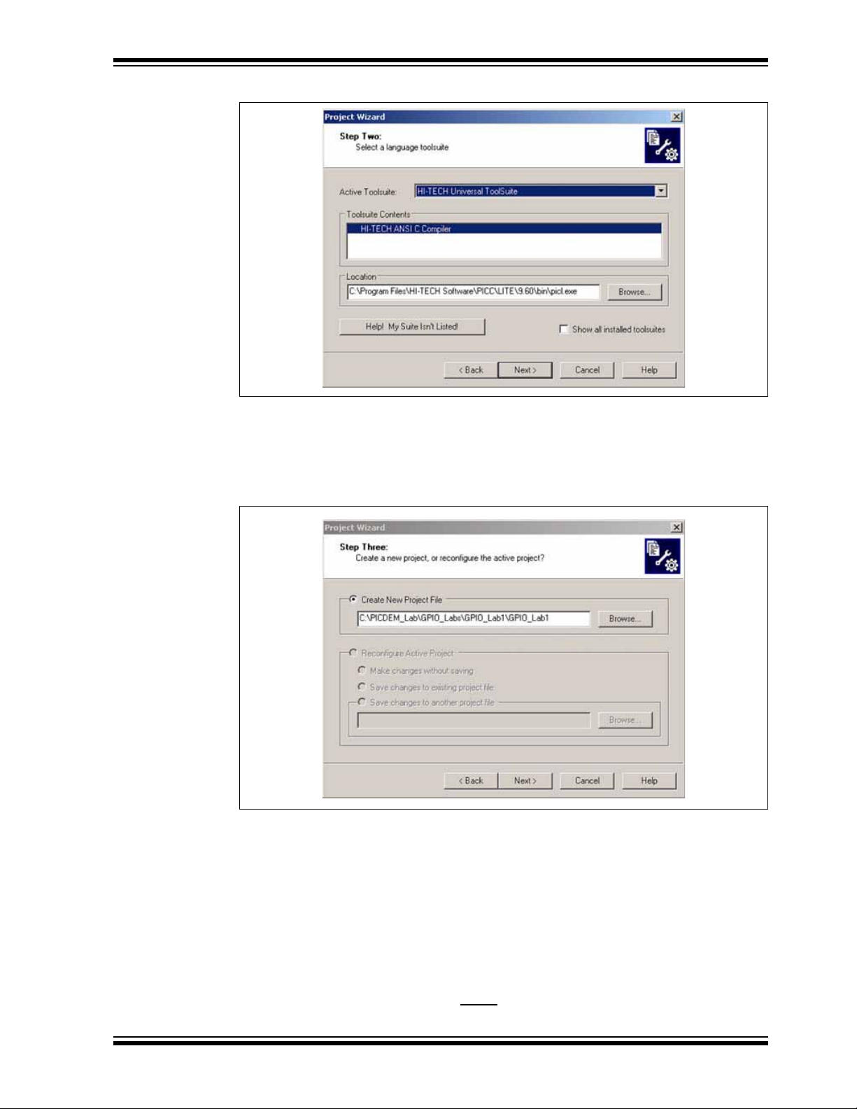
5. In the Step Two: window, select the HI TECH Universal ToolSuite from the Active
Toolsuite drop down menu. The window should now resemble Figure 3-4.
DS41369A-page 20 © 2009 Microchip Technology Inc.
Page 25
General Purpose Input/Output Labs
FIGURE 3-4: STEP TWO
6. In the Step Three: window, use the Browse button and navigate to a new folder
on the C:\ drive to store this project. Alternately, the reader may wish to use the
C:\PICDEM_Lab\GPIO_Labs\GPIO_Lab1 folder created earlier. (See
Figure 3-5.)
FIGURE 3-5: STEP THREE
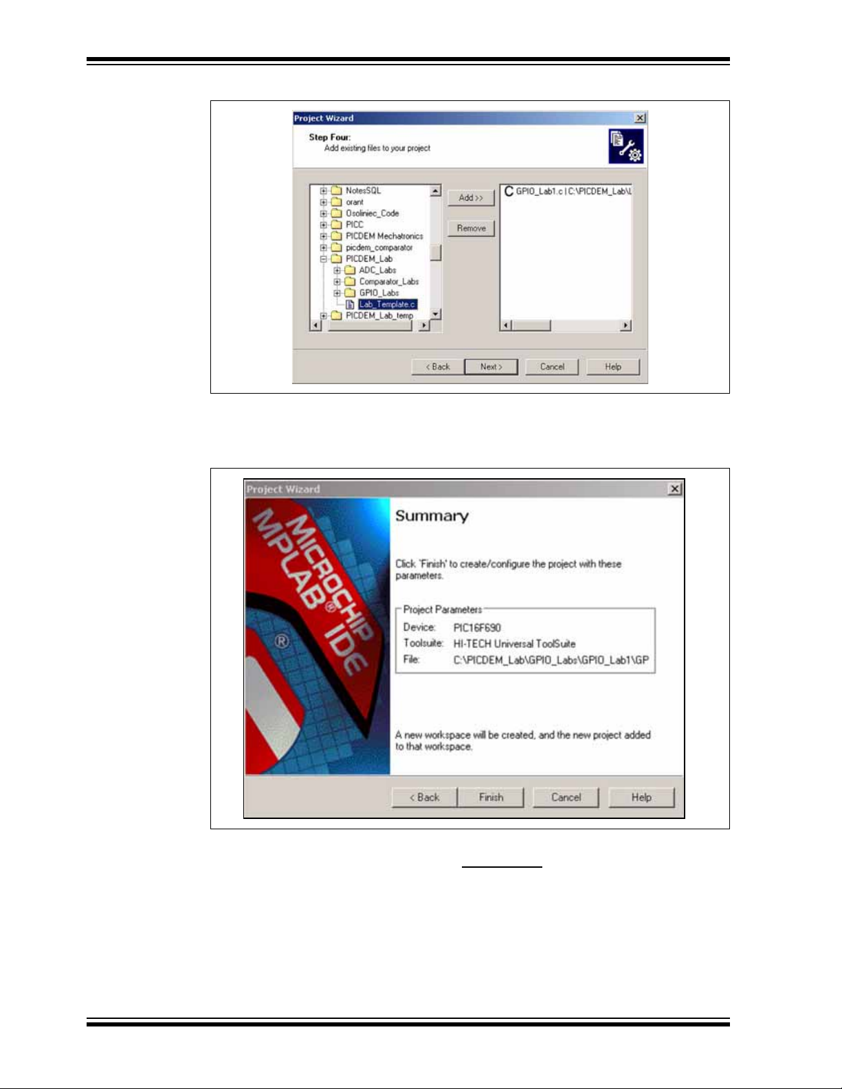
7. In the Step Four: files are added to the project. A Lab_Template.c file has
been provided in the C:\PICDEM_Lab\Lab_Template.c directory that can be
used as the basis for all labs in this manual. To use the Lab_Template.c file,
select it from the right menu and click the Add>> button. Click on the large letter
‘A’ that appears next to the added file in the right window until it becomes a ‘C’.
This indicates that a copy of the Lab_Template.c will be included in the project
directory. Otherwise, changes made to the file during the course of the lab will
alter the original file.
Finally, rename the Lab_Template.c file in the right window to GPIO_Lab1.c by
clicking on it three times to enable editing the name. The Step Four: window should
now resemble Figure 3-6. Click Next>
to continue.
© 2009 Microchip Technology Inc. DS41369A-page 21
Page 26
PICDEMTM Lab Development Board User’s Gu ide
FIGURE 3-6: STEP FOUR
8. Finally, the Summary window should appear showing the selected device, the
tool suite and the new project file name. Click Finish to exit the Project Wizard.
FIGURE 3-7: SUMMARY
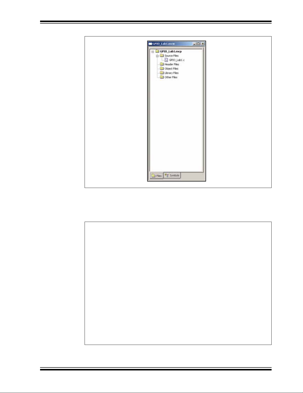
9. The MPLAB
visible, it can be opened by selecting View>Project
resemble Figure 3-8.
®
IDE Workspace should now be open. If the Project window is not
. The Project window should
DS41369A-page 22 © 2009 Microchip Technology Inc.
Page 27
General Purpose Input/Output Labs
//Clear PORTC to a known state
PORTC = 0b00000000;
//Configure PORTC's ANALOG/DIGITAL pins as all Digital
ANS4 = 0;//Associated with RC0
ANS5 = 0;//Associated with RC1
ANS6 = 0;//Associated with RC2
ANS7 = 0;//Associated with RC3
ANS8 = 0;//Associated with RC6
ANS9 = 0;//Associated with RC7
//Configure PORTC pins as all output
//i.e. 1 = Input, 0 = Output
TRISC0 = 0;//Make RC0 (pin 16) output
TRISC1 = 0;//Make RC1 (pin 15) output
TRISC2 = 0;//Make RC2 (pin 14) output
TRISC3 = 0;//Make RC3 (pin 7) output
TRISC4 = 0;//Make RC4 (pin 6) output
TRISC5 = 0;//Make RC5 (pin 5) output
TRISC6 = 0;//Make RC6 (pin 8) output
TRISC7 = 0;//Make RC7 (pin 9) output
FIGURE 3-8: PROJECT WIN DOW
10. Double click on the GPIO_Lab1.c source file in the Project window to open.
11. Copy/paste the code in Example 3-1 into the Initialize() section labeled:
//ADD INITIALIZE CODE HERE
EXAMPLE 3-1: INITIALIZE() CODE FOR LAB 1
© 2009 Microchip Technology Inc. DS41369A-page 23
Page 28

PICDEMTM Lab Development Board User’s Gu ide
RC0 = 1;//Make RC0 (pin 16) HIGH (approx. Vdd)
RC1 = 0;//Make RC1 (pin 15) LOW (approx. Vss)
RC2 = 1;//Make RC2 (pin 14) HIGH (approx. Vdd)
RC3 = 1;//Make RC3 (pin 7) HIGH (approx. Vdd)
RC4 = 0;//Make RC4 (pin 6) LOW (approx. Vss)
RC5 = 1;//Make RC5 (pin 5) HIGH (approx. Vdd)
RC6 = 0;//Make RC6 (pin 8) LOW (approx. Vss)
RC7 = 1;//Make RC7 (pin 9) HIGH (approx. Vdd)
Initialize(); //Initialize the relevant registers
while(1) //Code within curly braces will loop forever
{
Do_Outputs(); //Perform any outputs
}
12. Copy/paste the code in Example 3-2 into the Do_Outputs() section labeled:
//ADD DO_OUTPUTS CODE HERE
EXAMPLE 3-2: DO_OUTPUT() CODE FOR LAB 1
13. Copy/paste the code in Example 3-3 into the main() section labeled:
//ADD MAIN CODE HERE
EXAMPLE 3-3: MAIN() CODE FOR LAB 1
The project is now ready to compile and download to the PIC16F690.
14. Compile the project ensuring no errors.
15. Connect the PICkit™ 2 Programmer/Debugger to an available USB port on the
PC and then to the ICSP™ connector ICSP1 (J6) on the PICDEM Lab Development Board. The PICkit 2 should recognize if a power source is not connected to
the PIC16F690 and provide target power.
16. In the MPLAB™ IDE Project Workspace, select
Programmer>Select Programmer>PICkit 2
.
17. The PICkit 2 Programmer/Debugger toolbar should now be visible in the
workspace as shown in Figure 3-9.
DS41369A-page 24 © 2009 Microchip Technology Inc.
Page 29
General Purpose Input/Output Labs
Legend:
1. Program the target device
2. Read target device memories
3. Read the target EEDATA memory
4. Verify the contents of the target device
5. Erase the target device memories
6. Verify that target memories are erased
7. Bring target MCLR
to VDD
8. Bring target MCLR to VIL
9. Re-establish PICkit 2 connection
1 2 3 4 5 6 7 8 9
R8
470Ω
R4
470Ω
R7
470Ω
R6
470Ω
R5
470Ω
R3
470Ω
R2
470Ω
R1
470Ω
LED8 LED7 LED6 LED4 LED3 LED2 LED1LED5
V
SSLED ON LED OFF
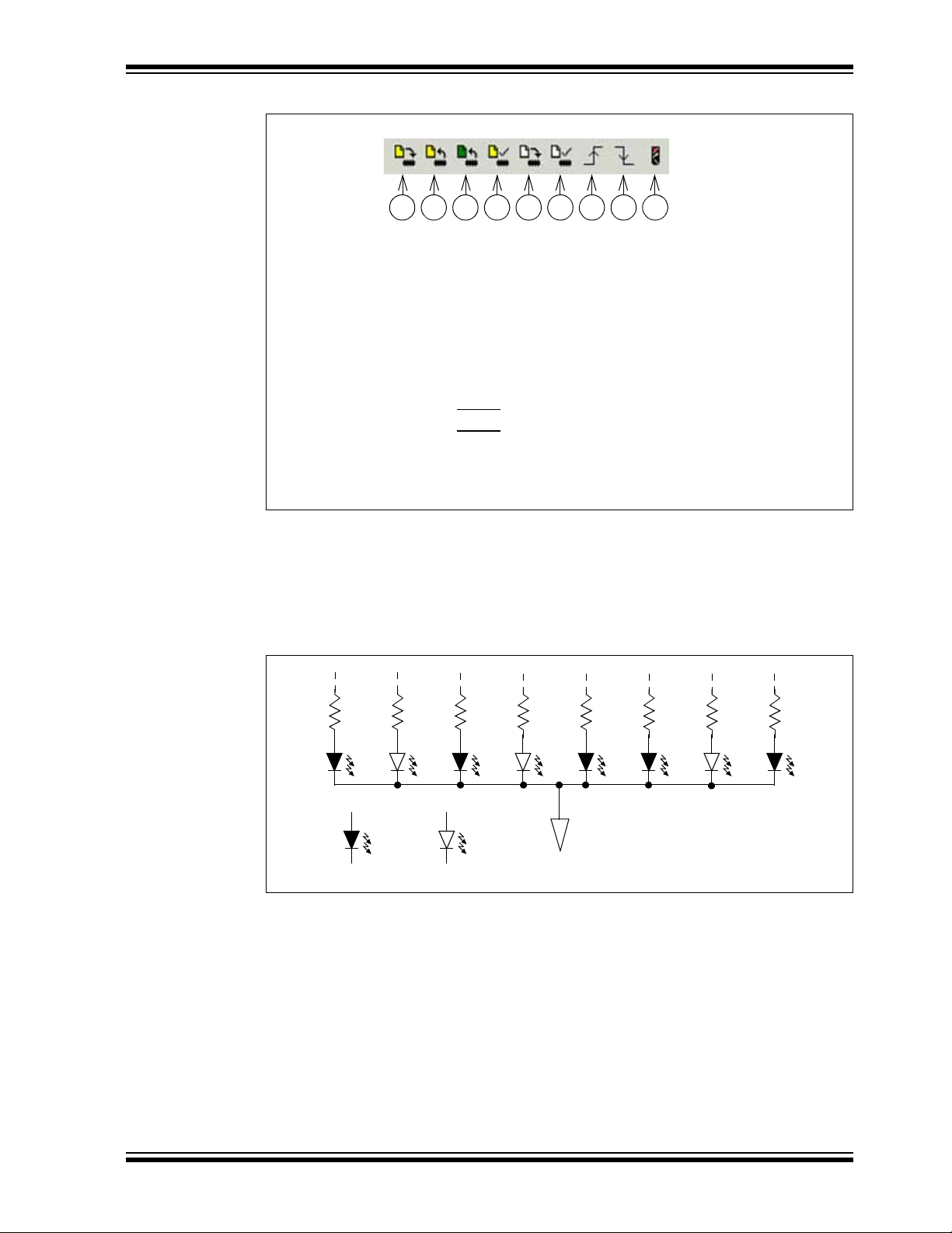
FIGURE 3-9: PICkit 2 PROGRAMMER/DEBUGGER TOOLBAR
© 2009 Microchip Technology Inc. DS41369A-page 25
8. Press button1 shown in Figure 3-9 to program the PIC16F690.
3.3.4.4 TESTING THE APPLICATION
Once programmed, the LEDs connected to the individual PORTC pins should now
resemble the output shown in Figure 3-10.
FIGURE 3-10: LAB 1 LED OUTPUT
The solution for this project is located in the
C:\PICDEM_Lab\GPIO_Labs\GPIO_Lab1\solution directory.
3.3.5 Lab 2: Flash LEDs (Delay Loop)
3.3.5.1 OVERVIEW
This lab implements a software delay to flash the LEDs connected to the PORTC pins
on/off in 1 second intervals. As configured, the PIC16F690 executes 1 million instructions per second. At this rate, the software loop execution needs to be slowed down so
that the LED flashing is visible to the eye. This is done using a delay routine within the
Timing() functional block called from the main() software control loop as shown in
Figure 3-11.
Page 30

PICDEMTM Lab Development Board User’s Gu ide
main()
Initialize()
Do_Outputs()
Loop Forever
Timing()
TIMING()
Create two 8-bit variables:
• delay_var1 = 45571
• delay_var2 = 3
delay_var2 - 1 = 0
?
delay_var1 - 1 = 0
?
END
delay_var1 = 45571
YES
YES
NO
NO
FIGURE 3-11: MAIN() SOFTWARE CONTROL LOOP FLOWCHART FOR
LAB 2
The Timing() delay routine is shown in Figure 3-12.
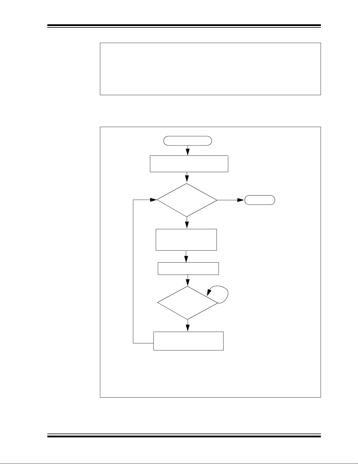
FIGURE 3-12: TIMING() DELAY ROUTINE FLOWCHART FOR LAB 2
Two variables are used delay_var1 and delay_var2. The delay_var2 is decremented by 1 each time delay_var1 is decremented from 45571 to 0. These values
have been determined through trial and error using a test procedure detailed in the
“Timers: Timer0 Tutorial (Part 1)” (DS51682.pdf) included on the PICDEM™ Lab
Development Kit CD. This delay ties the up the processor for 1 second when using the
4 MHz internal oscillator.
The Initialize() configures the PORTC as follows:
•PORTC
- Set all bits in the PORTC register HIGH
- Configure all PORTC pins as digital outputs
DS41369A-page 26 © 2009 Microchip Technology Inc.
Page 31

General Purpose Input/Output Labs
//Set all PORTC bits HIGH (to a known state)
PORTC = 0b11111111;
//Configure PORTC's ANALOG/DIGITAL pins as all Digital
ANS4 = 0;//Associated with RC0
ANS5 = 0;//Associated with RC1
ANS6 = 0;//Associated with RC2
ANS7 = 0;//Associated with RC3
ANS8 = 0;//Associated with RC6
ANS9 = 0;//Associated with RC7
//Configure PORTC pins as all output
//i.e. 1 = Input, 0 = Output
TRISC0 = 0;//Make RC0 (pin 16) output
TRISC1 = 0;//Make RC1 (pin 15) output
TRISC2 = 0;//Make RC2 (pin 14) output
TRISC3 = 0;//Make RC3 (pin 7) output
TRISC4 = 0;//Make RC4 (pin 6) output
TRISC5 = 0;//Make RC5 (pin 5) output
TRISC6 = 0;//Make RC6 (pin 8) output
TRISC7 = 0;//Make RC7 (pin 9) output
The Do_Outputs() changes somewhat from the previous lab by implementing the
XOR operator to toggle the value in each PORTC bit location each time through the
software loop. The XOR operator is implemented in code as follows:
RCx ^= 1;
This translates to: “Make RCx equal to the current value in RCx XOR’d with 1”
When a value is XOR’d with itself, the result is ‘0’ (i.e., 1 XOR’d with 1 = 0, 0 XOR’d
with 0 = 0). When a value is XOR’d with a value different than itself, the result is ‘1’ (i.e.,
1 XOR’d with 0 = 1). Therefore, each time through the loop PORTC bits will toggle from
1-to-0 or 0-to-1 depending on its current value.
3.3.5.2 PROCEDURE
Using the code developed in the previous lab, make the following changes:
1. Copy/paste the code in Example 3-4 over the Initialize() code from the
previous lab.
Note: The reader may wish to create a new project as per the previous lab called
GPIO_Lab2.mcp
EXAMPLE 3-4: INITIALIZE() CODE FOR LAB 2
The only change from the previous lab is that the PORTC bits are all set high to 1.
2. Copy/paste the code in Example 3-5 over the Do_Outputs() code from the
© 2009 Microchip Technology Inc. DS41369A-page 27
previous lab to accommodate the XOR bit toggle.
Page 32

PICDEMTM Lab Development Board User’s Gu ide
RC0 ^= 1;//XOR current RC0 value with 1
RC1 ^= 1;//XOR current RC1 value with 1
RC2 ^= 1;//XOR current RC2 value with 1
RC3 ^= 1;//XOR current RC3 value with 1
RC4 ^= 1;//XOR current RC4 value with 1
RC5 ^= 1;//XOR current RC5 value with 1
RC6 ^= 1;//XOR current RC6 value with 1
RC7 ^= 1;//XOR current RC7 value with 1
//--------DELAY 1second------------------------//Variable used in delay loop
unsigned int delay_var1 = 45571;
unsigned char delay_var2 = 3;
//Nested while loops to implement a 1 second delay
//Decrement delay_var2, if 0 jump out of loop
while(--delay_var2)
{
//Decrement delay_var1, if 0 jump out of loop
while(--delay_var1);
}
Initialize(); //Initialize the relevant registers
while(1)
{
Do_Outputs(); //Perform any outputs
Timing();//Sets execution rate of the
//Software Control Loop
}
EXAMPLE 3-5: DO_OUTPUT() CODE FOR LAB 2
3. Copy/paste the code in Example 3-6 into the Timing() section labeled:
//ADD TIMING CODE HERE
EXAMPLE 3-6: TIMING() FOR LAB 2
4. Copy/paste the code in Example 3-7 over the main() code from the previous lab
to incorporate the Timing().
EXAMPLE 3-7: MAIN() CODE FOR LAB 2
Compile the project. There should be no errors.
3.3.5.3 TESTING THE APPLICATION
DS41369A-page 28 © 2009 Microchip Technology Inc.
Program the PIC16F690. The LEDs connected to the individual PORTC pins should
now all flash on/off in 1 second intervals.
The solution for this project is located in the
C:\PICDEM_Lab\GPIO_Labs\GPIO_Lab2\solution directory.
Page 33

General Purpose Input/Output Labs
TMR0 Overflow Period = (4/FOSC) x 256 = 1 μSecond x 256 = 256 μSeconds
TMR0 Overflow Period = (4/FOSC) x 256 x prescaler
Using a 1:32 prescaler setting as an example and a 4 MHz internal oscillator
TMR0 Overflow Period = 1
μS x 256 x 32 = 8.192mS
3.3.6 Lab 3: Simple Delays Using Timer0
3.3.6.1 NEW REGISTERS USED IN THIS LAB
To configure the peripherals used in this lab, the following registers are used:
1. Timer0 Module Register: TMR0
- Holds a count value of the number of selected edge transition of a clock
source.
2. OPTION Register: OPTION_REG (Register 5-1 in Section 5 of the PIC16F690
Data Sheet).
- Selects clock source used to increment TMR0 result register.
- Selects clock source edge transition to increment TMR0.
3. Software configurable prescaler to determine the number of clock source edge
transitions before incrementing TMR0 register value.
4. Interrupt Control Register: INTCON (Register 2-3 in Section 2 of the PIC16F690
Data Sheet).
- Contains a flag that when 1, indicates a TMR0 register overflow has occurred.
3.3.6.2 OVERVIEW
To implement a more accurate delay, the Timer0 peripheral can be used. Timer0 is an
8-bit timer/counter that uses a clock source to increment an 8-bit register called TMR0.
Since this register is 8 bits, it can increment up 2
(00000000
TMR0 overflows, a Timer0 Overflow Flag (T0IF) in the OPTION register is set to ‘1’.
This register also features a prescaler that determines how many clock source cycles
it takes to increment TMR0 by ‘1’. In this way, simply by tracking the T0IF, very accurate
delays can be implemented. In this lab, the TMR0 register is configured to increment
on the low-to-high transition of an available internal instruction clock on the PIC16F690.
This internal instruction clock runs at the rate of the internal oscillator frequency F
divided by 4. Therefore, when the PIC16F690 is configured to operate using the internal 4 MHz oscillator, this internal instruction clock runs at a rate of
F
OSC/4 = 4MHz/4 = 1MHz. This is a period of 1/1MHz = 1 μS. If it is known that TMR0
increments every 1 μS, and it takes 256 internal instruction clock cycles to cause a
TMR0 overflow (i.e., 0-255 inclusive), then Equation 3-1 can be derived:
- 111111112) inclusive then rollover or overflow back to ‘0’. Whenever
2
8
= 256 times or 010 - 25510
OSC
EQUATION 3-1: TMR0 OVERFLOW PERIOD USING FOSC/4
As mentioned, Timer0 also features a prescaler that can be configured to increment the
value in TMR0 every 2, 4, 8, 16, 32, 64, 128, or 256 clock source transitions. Therefore,
this feature can be added to Equation 3-1 to create Equation 3-2.
EQUATION 3-2: TMR0 OVERFLOW PERIOD WHEN INCLUDING THE
PRESCALER
© 2009 Microchip Technology Inc. DS41369A-page 29
Page 34

PICDEMTM Lab Development Board User’s Gu ide
Desired TMR0 Overflow Period = (4/FOSC) x (256 - Preload Value) x prescaler
Using a 1:64 prescaler setting, a 4 MHz internal oscillator and requiring a 10 mS
overflow period:
10mS = 1
μSecond x (256 - Preload Value) x 64
10mS/(1
μSecond x 64) = 256 - Preload Value
Preload Value = 256 - [10mS/(1
μSecond x 64)]
Preload Value = 99.75 rounded up becomes 100
Therefore, to produce a 10 mS overflow period, using the internal instruction
clock with a 4 MHz internal oscillator and a TMR0 prescaler value of 1:64
requires that TMR0 be preloaded with a value of 100.
Delay_10mS()
END
YES
NO
Preload TMR0 register with 100
Clear the TMR0 overflow flag
(T0IF)
T0IF = 0?
Finally, TMR0 is a writable register. Meaning that a value can be added to the register
to offset the number of counts it takes for the overflow to occur. Equation 3-3 demon-
strates how to calculate the value to preload the TMR0 register with to create a 10mS
overflow period.
EQUATION 3-3: CALCULATING A TMR0 PRELOAD VALUE TO GENERATE A
10MS OVERFLOW PERIO D
The software flowchart to implement a 10mS delay is shown in Figure 3-13.
FIGURE 3-13: DELAY_10MS() USING TIMER0
The maximum overflow period that can be achieved using Timer0 only utilizes a 1:256
prescaler is as shown in Equation 3-4.
DS41369A-page 30 © 2009 Microchip Technology Inc.
Page 35
General Purpose Input/Output Labs
TMR0 Overflow Period = (4/FOSC) x 256 x prescaler
using a maximum prescaler setting of 1:256 and the 4MHz internal oscillator
TMR0 Overflow Period = 1 μS x 256 x 256 = 65.5mS
Delay_1S()
END
YES
NO
counter variable value determined as follows:
1 second/65.5mS = 15.25 or rounded down to 15
Create an 8-bit variable counter and
initialize to 0
Clear the TMR0 register
Clear the TMR0 overflow flag
(T0IF)
T0IF = 0?
counter < or = 15?
Increment counter value by 1
NO
YES
EQUATION 3-4: MAXIMUM TMR0 OVERFLOW PERIOD
Therefore, to implement delays greater than 65.5mS, a counter variable is
implemented as shown in the flowchart of Figure 3-14 for a 1 second delay.
FIGURE 3-14: DELAY_1S() USING TIMER0
© 2009 Microchip Technology Inc. DS41369A-page 31
Page 36

PICDEMTM Lab Development Board User’s Gu ide
/*---------------------------------------------------------
Subroutine: Delay_1S
Parameters: none
Returns:nothing
Synopsis:Creates a 1S delay when called
---------------------------------------------------------*/
void Delay_1S(void)
{
//Create an 8-bit variable called counter
//and initialize it to 0
unsigned char counter = 0;
while(counter <= 15)
{
//Make sure the T0IF is cleared
T0IF = 0;
//Clear the TMR0 register
TMR0 = 0;
//Sit here and wait for Timer0 to overflow
while (T0IF == 0);
++counter;
}
}
The Initialize() now configures the PIC16F690 peripherals as follows:
•PORTC
- Set all bits in PORTC high
- Make all PORTC pins digital output
•Timer0
- Use the internal instruction clock (F
- Increment TMR0 register on low-to-high transition of F
- Assign the prescaler to Timer0 and configure to increment on every 256th
transition of F
OSC/4
3.3.6.3 PROCEDURE
Using the firmware developed in the previous lab, make the following changes:
1. Copy/paste the code in Example 3-8 at the top of the main firmware source file
under the heading labeled:
/**SUPPORT ROUTINES**********************************/
EXAMPLE 3-8: DELAY_1S() CODE FOR LAB 3
OSC/4) as the TMR0 register clock source
OSC/4
DS41369A-page 32 © 2009 Microchip Technology Inc.
2. Copy/paste the code in Example 3-9 into the Initialize() over the code from
the previous lab.
Page 37

General Purpose Input/Output Labs
//Set all PORTC bits HIGH (to a known state)
PORTC = 0b11111111;
//Configure PORTC's ANALOG/DIGITAL pins as all Digital
ANS4 = 0;//Associated with RC0
ANS5 = 0;//Associated with RC1
ANS6 = 0;//Associated with RC2
ANS7 = 0;//Associated with RC3
ANS8 = 0;//Associated with RC6
ANS9 = 0;//Associated with RC7
//Configure PORTC pins as all output
//i.e. 1 = Input, 0 = Output
TRISC0 = 0;//Make RC0 (pin 16) output
TRISC1 = 0;//Make RC1 (pin 15) output
TRISC2 = 0;//Make RC2 (pin 14) output
TRISC3 = 0;//Make RC3 (pin 7) output
TRISC4 = 0;//Make RC4 (pin 6) output
TRISC5 = 0;//Make RC5 (pin 5) output
TRISC6 = 0;//Make RC6 (pin 8) output
TRISC7 = 0;//Make RC7 (pin 9) output
//Configure Timer0 as follows:
T0CS = 0; //Use the internal instruction clock
//FOSC/4 as the clock source
T0SE = 0;//Increment TMR0 on low-to-high
//FOSC/4 transition
PSA = 0;//Assign the prescaler to
//Timer0
//Configure Timer0 prescaler to increment
//TMR0 every 256 FOSC/4 clock transitions
PS0 = 1;
PS1 = 1;
PS2 = 1;
Delay_1S(); //Call the 1 second delay
EXAMPLE 3-9: INITIALIZE() CODE FOR LAB 3
3. Finally, copy/paste the code in Example 3-10 into the Timing() over the code
from the previous lab
EXAMPLE 3-10: TIMING() CODE FOR LAB 3
4. The remaining code from the previous lab remains the same. Compile the proj-
ect. There should be no errors.
3.3.6.4 TESTING THE APPLICATION
Program the PIC16F690. The application should behave exactly as it did in the
previous lab. Using an oscilloscope to test individual PORTC pin level transitions would
be useful to analyze the accuracy of the delay.
The solution for this project is located in the
C:\PICDEM_Lab\GPIO_Labs\GPIO_Lab3\solution directory.
Note: More in-depth tutorials on the Timer0 peripheral are covered in “Timers:
Timer0 Tutorial (Part 1)” (5162a.pdf) and “Timers: Timer0 Tutorial (Part 2)”
(51702a.pdf) files included on the PICDEM™ Lab Development Kit CD.
© 2009 Microchip Technology Inc. DS41369A-page 33
Page 38

PICDEMTM Lab Development Board User’s Gu ide
main()
Initialize()
Do_Outputs()
Loop Forever
Timing()
Decide()
Global Variables:
• 8-bit LED_Output
Decide()
LED_Output = 0b10000000
or
LED_Output = 0b00000000
?
END
Shift contents of LED_Output
variable left by 1 bit position
YES
NO
LED_Output = 0b00000001
LED_Output variable initialize to 0b00000001
in Initialize()
3.3.7 Lab 4: Rotate LEDs
3.3.7.1 OVERVIEW
This lab shifts a high bit in the PORTC register from right-to-left each time through the
software loop sequentially lighting the LEDs connected to the PORTC pins in 1 second
intervals as dictated by the Timing(). This lab adds some new functional blocks to
the main() software control loop as shown in Figure 3-15.
FIGURE 3-15: MAIN() SOFTWARE CONTROL LOOP FLOWCHART FOR
LAB 4
DS41369A-page 34 © 2009 Microchip Technology Inc.
The addition of an 8-bit global variable (can be manipulated by any function) called
LED_Output is used. This variable will be acted upon by the new Decide() by shifting a high bit in LED_Output from right-to-left each time this function is called. The
flowchart for the Decide() is shown in Figure 3-16.
FIGURE 3-16: DECIDE() FLOWCHART FOR LAB 4
Page 39
General Purpose Input/Output Labs
Do_Outputs()
assigns
LED_Output to
PORTC
LED_Output variable
10000000
10000000
PORTC
Do_Outputs()
assigns
LED_Output to
PORTC
01000000
01000000
LED_Output variable
PORTC
Decide() shifts contents of
LED_Output Left by 1 bit position
Corresponding LED lights
Corresponding LED lights
First time through main():
Next time through main():
Initialize() determines initial
contents of LED_Output
The Decide() first checks the current value in LED_Output for two specific conditions:
• Is the Most Significant bit ‘1’? This means that on the next shift, the contents will
be all ‘0’s.
• Is the value currently a ‘0’?
If either condition exists, the function re-initializes LED_Output to set the Least Significant bit. Otherwise, there will be a period when none of the LEDs are lit.
The shift is implemented in code as follows:
LED_Output <<= 1;
This translates to: “LED_Output is equal to the current contents of LED_Output
shifted to the left by 1 bit position”
Conversely, to shift the bit to the right the code would be as follows:
LED_Output >>= 1;
The Do_Outputs() will then assign the contents of the LED_Output variable to the
PORTC register and whichever bit is high will light the connected LED. (See
Figure 3-17.)
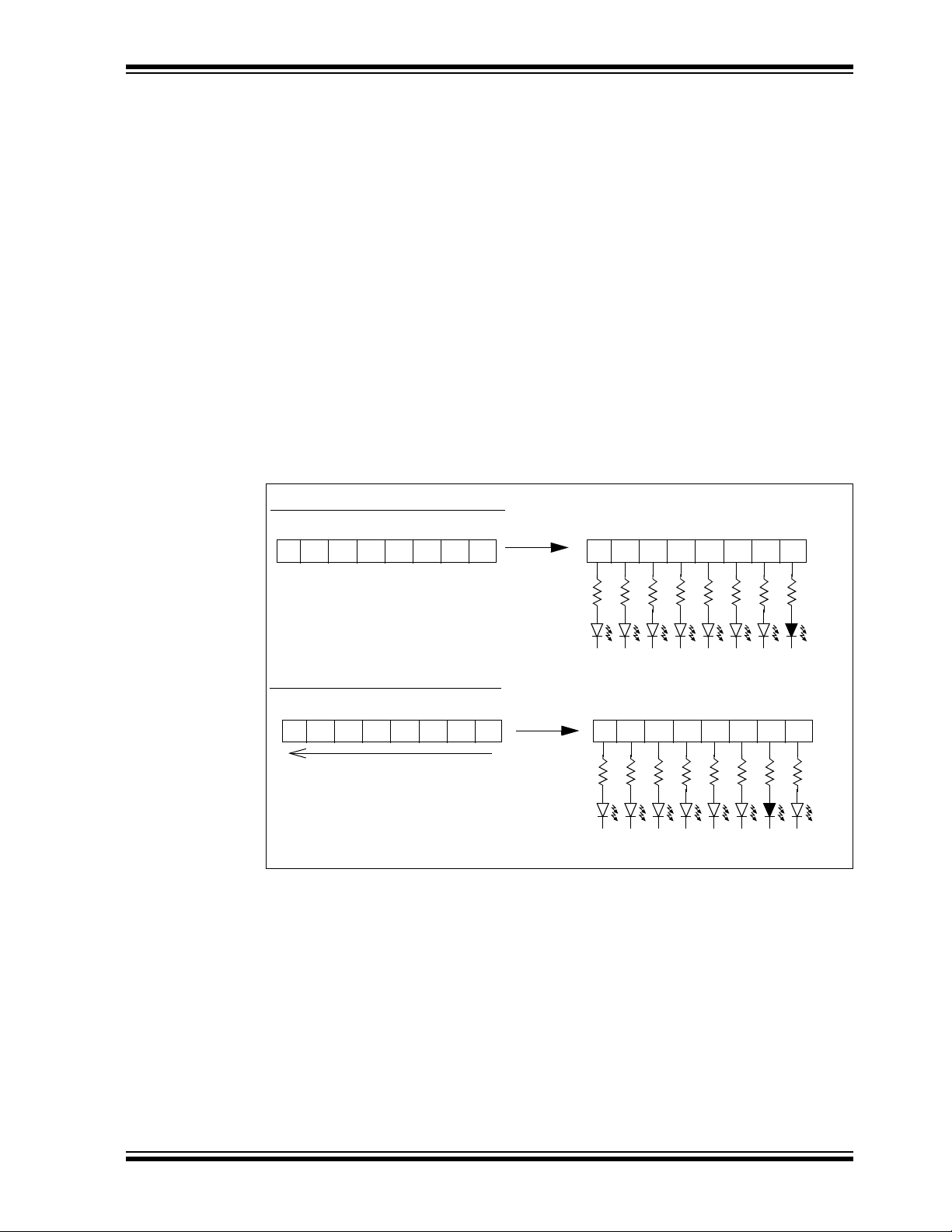
FIGURE 3-17: RESULTS OF DO_OUTPUT()
© 2009 Microchip Technology Inc. DS41369A-page 35
The Initialize() now configures the PIC16F690 peripherals as follows:
•PORTC
- Initialize PORTC so that the 7 Most Significant bits are ‘0’ and the Least
Significant bit is ‘1’
- Make all PORTC pins digital output
•Timer0
- Use the internal instruction clock (F
- Increment TMR0 register on low-to-high transition of F
- Assign the prescaler to Timer0 and configure to increment on every 256th
• Initialize the LED_Output variable to ‘0’
transition of F
OSC/4
OSC/4) as the TMR0 register clock source
OSC/4
Page 40

PICDEMTM Lab Development Board User’s Gu ide
unsigned char LED_Output;//Variable used to set/clear PORTC bits
//Clear PORTC to a known state
PORTC = 0b00000001;
//Configure PORTC's ANALOG/DIGITAL pins as all Digital
ANS4 = 0;//Associated with RC0
ANS5 = 0;//Associated with RC1
ANS6 = 0;//Associated with RC2
ANS7 = 0;//Associated with RC3
ANS8 = 0;//Associated with RC6
ANS9 = 0;//Associated with RC7
//Configure PORTC pins as all output
//i.e. 1 = Input, 0 = Output
TRISC0 = 0;//Associated with RC0
TRISC1 = 0;//Associated with RC1
TRISC2 = 0;//Associated with RC2
TRISC3 = 0;//Associated with RC3
TRISC4 = 0;//Associated with RC4
TRISC5 = 0;//Associated with RC5
TRISC6 = 0;//Associated with RC6
TRISC7 = 0;//Associated with RC7
//Configure Timer0 as follows:
T0CS = 0; //Use the internal instruction clock
//FOSC/4 as the clock source
T0SE = 0;//Increment TMR0 on low-to-high
//FOSC/4 transition
PSA = 0;//Assign the prescaler to
//Timer0
//Configure Timer0 prescaler to increment
//TMR0 every 256 FOSC/4 clock transitions
PS0 = 1;
PS1 = 1;
PS2 = 1;
//Initialize LED_Output to all zeros
LED_Output = 0b00000000;
3.3.7.2 PROCEDURE
Using the code developed in the previous lab, make the following changes:
1. The LED_Output variable will need to be declared before it can be used.
Copy/paste the code in Example 3-11 to the beginning of the source file under
the section marked:
//-----------------DATA MEMORY------------------------
EXAMPLE 3-11: LED_OUTPUT VARIABLE DECLARATION FOR LAB 4
2. Copy/paste the code in Example 3-12 over the Initialize() code from the
previous lab.
EXAMPLE 3-12: INITIALIZE() CODE FOR LAB 4
DS41369A-page 36 © 2009 Microchip Technology Inc.
Page 41

General Purpose Input/Output Labs
//First check if LED_Output variable has most significant bit
//set to 1 or if LED_Output variable is all 0's.
//If so, re initialize the LED_Output variable so that the
//least significant bit is set to 1 and all other bits are
//cleared to 0
if((LED_Output == 0b10000000) || (LED_Output == 0b00000000))
LED_Output = 0b00000001;
//If neither of these conditions are true, simply shift
//the LED_Output variable's contents to the Left by 1 bit
//position
else LED_Output <<=1;
//Assign the manipulated contents of the
//LED_Output variable to the PORTC register
PORTC = LED_Output;
Initialize(); //Initialize the relevant registers
while(1)
{
Decide(); //Make any decisions
Do_Outputs(); //Perform any outputs
Timing();//Sets execution rate of the
//Software Control Loop
}
Changes from the previous lab include PORTC initialization so that all bits are ‘0’
except for the Least Significant bit (LSb) and the initialization of the LED_Output
variable.
3. Copy/paste the code in Example 3-13 into the Decide() section labeled:
//ADD DECISION CODE HERE
EXAMPLE 3-13: DECIDE()CODE FOR LAB 4
4. Copy/paste the code in Example 3-14 over the Do_Outputs() code from the
previous lab.
EXAMPLE 3-14: DO_OUTPUTS() CODE FOR LAB 4
This code simply assigns the contents of the LED_Output variable to the PORTC
register.
5. Copy/paste the code in Example 3-15 over the main() code from the previous
lab to incorporate the Decide().
EXAMPLE 3-15: MAIN() CODE FOR LAB 4
© 2009 Microchip Technology Inc. DS41369A-page 37
Compile the project. There should be no errors.
Page 42

PICDEMTM Lab Development Board User’s Gu ide
3.3.7.3 TESTING THE APPLICATION
Program the PIC16F690. The LEDs connected to the individual PORTC pins should
now all flash on/off sequentially from right-to-left in 1 second intervals.
The solution for this project is located in the
C:\PICDEM_Lab\GPIO_Labs\GPIO_Lab4\solution directory.
3.4 GPIO INPUT LABS
3.4.1 Reference Documentation
PIC16F690 Data Sheet
• Section 2: Memory Organization
• Section 4: I/O Ports
• Section 5: Timer0 Module
3.4.2 Equipment Required for GPIO Input Labs
To complete the labs in this section, the following components are required:
1. 1 – push button
2. 8 – Light Emitting Diodes
3. 1 – 10 K
4. 8 – 470Ω resistors
5. PIC16F690 populating socket U2
6. Assorted jumper wires
Ω
3.4.3 PICDEM Lab Development Board Setup for GPIO Input Labs
The GPIO input labs will require that the PICDEM Lab Development Board be
configured as shown in Figure 3-12 using the components listed in the previous
section.
DS41369A-page 38 © 2009 Microchip Technology Inc.
Page 43

General Purpose Input/Output Labs
U2
1
2
3
4
5
6
7
8
9
10
20
19
18
17
16
15
14
13
12
11
RC0
RC1
RC2
RC3
RC4
RC5
RC6
RC7
J9J8
R8
470Ω
R4
470Ω
R7
470Ω
R6
470Ω
R5
470Ω
R3
470Ω
R2
470Ω
R1
470Ω
LED8 LED7 LED6 LED4 LED3 LED2 LED1LED5
V
SS
V
SS
V
DD
R9
10KΩ
SW1
RA2
FIGURE 3-18: PICDEM LAB SCHEMATIC FOR GPIO INPUT LABS
The only change from the previous section is the inclusion of a push button connected
to RA2 with associated pull-up resistor.
3.4.4 Lab 5: Adding a Push Button
3.4.4.1 NEW REGISTERS USED IN THIS LAB
To configure the peripherals used in this lab, the following registers are used:
1. PORTA Register: PORTA (Register 4-1 in Section 4 of the PIC16F690 Data
Sheet)
- 8-bit bidirectional port
2. PORTA Tri-State Register: TRISA (Register 4-2 in Section 4 of the PIC16F690
Data Sheet)
- Configures corresponding bits in PORTA as either input or output
3.4.4.2 OVERVIEW
This lab expands upon Lab 4 by adding a push button interface to change the direction
of the sequential shift in the PORTC register.
Mechanical switches play an important and extensive role in practically every
computer, microprocessor and microcontroller application. Mechanical switches are
inexpensive, simple and reliable. However, switches can be very noisy electrically. The
apparent noise is caused by the closing and opening action that seldom results in a
clean electrical transition. The connection makes and breaks several, perhaps even
hundreds, of times before the final switch state settles. The problem is known as switch
bounce. Some of the intermittent activity is due to the switch contacts actually bouncing
off each other. Also, switch contacts are not perfectly smooth. As the contacts move
against each other, the imperfections and impurities on the surfaces cause the
electrical connection to be interrupted. The result is switch bounce. The consequences
© 2009 Microchip Technology Inc. DS41369A-page 39
Page 44

PICDEMTM Lab Development Board User’s Gu ide
main()
Initialize()
Do_Outputs()
Loop Forever
Timing()
Decide()
Global Variables:
• 8-bit variable LED_Output will be used to
light the LEDs connected to PORTC
• 1-bit variable direction used to determine the direction of the s e que ntial LED
flashing
0 = shift PORTC bits right-to-left
1 = shift PORTC bits left-to-right
Get_Inputs()
of uncorrected switch bounce can range from being just annoying to catastrophic. The
classic solution involves filtering, such as through a resistor-capacitor circuit, or through
resettable shift registers. These methods are still effective but they involve additional
cost in material, installation and board real estate. Debouncing in software eliminates
these additional costs.
One of the simplest ways to switch debounce is to sample the switch until the signal is
stable or continue to sample the signal until no more bounces are detected. How long
to continue sampling requires some investigation. However, 5 mS is usually adequate,
while still reacting fast enough that the user won't notice it.
The software flowchart for this application is shown in Figure 3-19.
FIGURE 3-19: MAIN() SOFTWARE CONTROL LOOP FLOWCHART FOR
LAB 5
The Initialize() now configures the following:
•PORTC
- Configure PORTC pins as per the previous labs
•PORTA
- Clear PORTA register.
- Configure RA2 as a digital input pin
• Timer0 will be configured to implement the 5mS delay as follows:
- Use the internal instruction clock F
- Increment TMR0 on the low-to-high transition of F
- Assign the prescaler to TMR0 and configure 1:64.
• Initialize the LED_Output variable to ‘0’
• Initialize the direction bit variable to ‘0’
- This is a global variable that will be manipulated by the new Get_Inputs()
DS41369A-page 40 © 2009 Microchip Technology Inc.
(see Registers 4-1 and 4-2 in Section 4.1 of the PIC16F690 Data Sheet).
OSC/4 as the TMR0 clock source.
OSC/4.
and used to determine PORTC shift direction by the Decide().
Page 45

General Purpose Input/Output Labs
Get_Inputs()
RA0 = 0
?
END
Contents of direction
remain unchanged
YES
NO
Delay_5mS()
RA0 = 0
?
Toggle contents of
direction
YES
NO
Debounces signal
on RA2
A new function called Get_Inputs() is used to check the RA2 pin voltage. Referring
to Figure 3-12, the RA2 pin connected to the push button (SW1) is pulled to V
a 10 KΩ
resistor. This pull-up resistor eliminates noise on the pin that could trigger
“false” push button presses. The second terminal of the push button is connected to
V
SS. In this way, when a user presses the push button the voltage present on RA2 will
transition from V
DD
(high or ‘1’) to VSS (low or ‘0’). The software flowchart for the
Get_Inputs() is shown in Figure 3-20.
FIGURE 3-20: GET_INPUTS() SOFTWARE FLOWCHART FOR LAB 5
DD using
Referring to the flowchart in Figure 3-20, the Get_Inputs() first checks the voltage
level on the RA2 pin. If the voltage is logic low (= 0 or V
SS), a 5mS delay is implemented
using a new support routine called Delay_5mS() to allow any switch bouncing to settle. The Delay_5mS() is based off of the Timer0 peripheral as discussed in Lab 3. The
software flowchart for Delay_5mS() is shown in Figure 3-21.
© 2009 Microchip Technology Inc. DS41369A-page 41
Page 46

PICDEMTM Lab Development Board User’s Gu ide
Delay_5mS()
T0IF = 1
(i.e., TMR0 overflow)
?
END
Clear the Timer0 overflow
flag (T0IF)
YES
NO
Preload the Timer0 result
register (TMR0) with 100
Timer0 configured in the Initialize() as fol-
lows:
• Using the internal F
OSC/4 (4MHz/4) clock
source
• TMR0 increments on low-to-high transition
of F
OSC/4
• Prescaler configured for 1:32
Desired Timer0 Overflow Rate = (4/F
OSC) x number of counts to overflow x prescaler
5mS = 1μSeconds x (256 – TMR 0 preload value) x 32
TMR0 preload value = 256 – 5mS = 99.75 rounded to 100
1μSeconds x 32
TMR0 preload valu e det er m ined as follows:
FIGURE 3-21: DELAY_5MS() SOFTWARE FLOWCHART FOR LAB 5
The RA2 pin voltage is then checked again. If still low, a push button press is indicated
and the direction bit variable is toggled. Otherwise, the direction value stays the
same.
The Decide() then uses the current direction value to determine which direction
to shift the contents of the LED_Output global variable. The Decide() software
flowchart is shown in Figure 3-22.
DS41369A-page 42 © 2009 Microchip Technology Inc.
Page 47

General Purpose Input/Output Labs
Decide()
direction = 0
?
END
LED_Output =
0b00000001
YES
NO
Shift contents of
LED_Output left
by 1 bit position
NO
YES
LED_Output = 0b10000000
or
LED_Output = 0b00000000
?
YES
NO
LED_Output = 0b10000000
Shift contents of
LED_Output right
by 1 bit position
LED_Output = 0b00000001
or
LED_Output = 0b00000000
?
unsigned char LED_Output;//Variable used to set/clear PORTC bits
bit direction;//Variable to select direction of shifting LEDs
FIGURE 3-22: DECIDE() SOFTWARE FLOWCHART FOR LAB 5
Similar to the previous lab, Decide() checks the LED_Output variable value before
executing the shift to ensure that the variable is not all 0’s or that the Most Significant
bit, for a left shift, or Least Significant bit, for a right shift, are not ‘1’, indicating that the
shift that follows will fill the LED_Output variable with 0’s.
The Do_Outputs() simply assigns the contents of the LED_Output variable to the
PORTC register lighting the connected LEDs accordingly.
3.4.4.3 PROCEDURE
Using the firmware developed in the previous lab, make the following changes:
Copy/paste the code in Example 3-16 into the top of the firmware source template under the
section marked:
//--------------------DATA MEMORY----------------------
EXAMPLE 3-16: VARIABLE DECLARATIONS FOR LAB 5
© 2009 Microchip Technology Inc. DS41369A-page 43
Page 48

PICDEMTM Lab Development Board User’s Gu ide
/*---------------------------------------------------------
Subroutine: Delay_5mS
Parameters: none
Returns:nothing
Synopsis:Creates a 5mS delay when called
---------------------------------------------------------*/
void Delay_5mS(void)
{
//Make sure the T0IF is cleared
T0IF = 0;
//preload the TMR0 register
TMR0 = 100;
//Sit here and wait for Timer0 to overflow
while (T0IF == 0);
}
1. Copy/paste the function code in Example 3-17 into the top of the firmware source
template under the section marked:
/**SUPPORT ROUTINES*************************************
EXAMPLE 3-17: DELAY_5MS() CODE FOR LAB 5
2. Copy/paste the code in Example 3-18 into the Initialize() over the code
from the previous lab.
DS41369A-page 44 © 2009 Microchip Technology Inc.
Page 49

General Purpose Input/Output Labs
//Clear PORTC to a known state
//Set the least significant bit to 1 so that it can be
//shifted through
PORTC = 0b00000001;
//Clear the PORTA register to a known state
PORTA = 0b00000000;
//Configure PORTC's ANALOG/DIGITAL pins as all Digital
ANS4 = 0;//Associated with RC0
ANS5 = 0;//Associated with RC1
ANS6 = 0;//Associated with RC2
ANS7 = 0;//Associated with RC3
ANS8 = 0;//Associated with RC6
ANS9 = 0;//Associated with RC7
//Configure PORTC pins as all output
//i.e. 1 = Input, 0 = Output
TRISC0 = 0;//Associated with RC0
TRISC1 = 0;//Associated with RC1
TRISC2 = 0;//Associated with RC2
TRISC3 = 0;//Associated with RC3
TRISC4 = 0;//Associated with RC4
TRISC5 = 0;//Associated with RC5
TRISC6 = 0;//Associated with RC6
TRISC7 = 0;//Associated with RC7
//Configure PORTA bit RA0 as Digital input
ANS2 = 0;
TRISA2 = 1;
//Configure Timer0 to overflow every 5mS
T0CS = 0; //Select FOSC/4 as Timer0 clock source
T0SE = 0; //Increment TMR0 on rising clock edge
PSA = 0; //Assign prescaler to Timer0
//Select a 1:32 prescaler
PS0 = 0;
PS1 = 0;
PS2 = 1;
//Initialize the direction flag to shift bits from
//right-to-left
//(i.e. 0 = Shift PORTC bits from right-to-left
// 1 = Shift PORTC bits from left-to-right
direction = 0;
//Initialize LED_Output to all zeros
LED_Output = 0b00000000;
EXAMPLE 3-18: INITIALIZE() FOR GPIO LAB 5
© 2009 Microchip Technology Inc. DS41369A-page 45
Page 50

PICDEMTM Lab Development Board User’s Gu ide
//Check for a push button press (i.e. RA2 = 0)
if (RA2 == 0)
{
Delay_5mS(); //Delay to debounce
//Check if push button is still pressed
if(RA2 == 0) direction ^= 1; //If so, toggle the
//direction bit
}
//Otherwise keep direction the same as it was
else direction = direction;
if(direction == 0)
{
//First check if LED_Output variable has most
//significant bit set to 1 or if LED_Output variable is
//all 0's.
//If so, re initialize the LED_Output variable so that
//the most significant bit is set to 1 and all other
//bits are 0
if((LED_Output == 0b00000001) || (LED_Output ==
0b00000000)) LED_Output = 0b10000000;
//If neither of these conditions are true, simply shift
//the LED_Output variable's contents to the Left by 1
//bit position
else LED_Output >>=1;
}
else
{
//First check if LED_Output variable has the least
//significant bit set
//to 1 or if LED_Output variable is all 0's.
//If so, re initialize the LED_Output variable so that
//the least significant bit is set to 1 and all other
//bits are 0
if((LED_Output == 0b10000000) || (LED_Output ==
0b00000000)) LED_Output = 0b00000001;
//If neither of these conditions are true, simply shift
//the LED_Output variable's contents to the Right by 1
//bit position
else LED_Output <<=1;
}
3. Copy/paste the code in Example 3-19 into the Get_Inputs() at the section
labeled:
//ADD GET_INPUTS CODE HERE
EXAMPLE 3-19: GET_INPUTS() CODE FOR GPIO LAB 5
4. Copy/paste the code in Example 3-20 into the Decide() over the code from the
previous lab.
EXAMPLE 3-20: DECIDE() CODE FOR GPIO LAB 5
DS41369A-page 46 © 2009 Microchip Technology Inc.
Page 51

General Purpose Input/Output Labs
unsigned int delay_var = 9997;
//Keep looping until the delay_var is
// equal to zero (should take 10mS)
while(--delay_var);
Initialize(); //Initialize the relevant registers
while(1)
{
Get_Inputs();//Evaluate inputs
Decide();//Make any decisions
Do_Outputs(); //Perform any outputs
Timing();//Sets execution rate of the
//Software Control Loop
}
5. The Do_Outputs() code from the previous lab stays the same.
6. Copy/paste the code in Example 3-21 into the Timing() over the code from the
previous lab.
EXAMPLE 3-21: TIMING() CODE FOR GPIO LAB 5
Note: This lab now utilizes a 10 mS delay to time the software control loop.
7. Copy/paste the code in Example 3-22 over the main() code from the previous
lab.
EXAMPLE 3-22: MAIN() CODE FOR LAB 5
8. Compile the project, there should be no errors.
3.4.4.4 TESTING THE APPLICATION
Program the PIC16F690. Once programmed, the LEDs connected to PORTC should
sequentially light from left-to-right in 10 mS intervals. When the push button is pressed,
the LEDs should change directions and sequentially light from right-to-left.
Continuously pressing the push button will change the direction each time.
It should be noted that the push button press inconsistently changes the direction of
sequential flashing. The problem here is that the firmware performs a technique called
"Polling" to check the state of the RA0 pin that connects to the push button. Therefore,
the state of RA0 is checked only once each time through the software control loop when
the Get_Inputs() is called. This polling is subject to the timing of the software control loop and will lead to push button presses being missed. If the Timing() remained
at the 1 second delay as implemented in the previous lab, this would have made
matters worse. The next labs will remedy these issues through the use of interrupts.
The solution for this project is located in the
C:\PICDEM_Lab\GPIO_Labs\GPIO_Lab5\solution directory.
© 2009 Microchip Technology Inc. DS41369A-page 47
Page 52

PICDEMTM Lab Development Board User’s Gu ide
3.4.5 Lab 6: Push Button Interrupt
3.4.5.1 NEW REGISTERS USED IN THIS LAB
To configure the peripherals used in this lab, the following registers are used:
1. OPTION Register: OPTION (Register 2-2 in Section 2 of the PIC16F690 Data
Sheet)
- Selects the edge transition on RA2/INT that will trigger an interrupt.
2. Interrupt Control Register: INTCON (Register 2-3 in Section 2 of the PIC16F690
Data Sheet)
- Enable interrupt functionality on the PIC16F690.
- Enables the RA2/INT external interrupt.
- Contains a flag that indicates the external interrupt has occurred.
3.4.5.2 OVERVIEW
This lab expands upon Lab 5 by adding an interrupt that will occur each time the push
button connected to the RA2 pin is pressed.
As mentioned, polling a bit is heavily reliant on a number of factors such as the size of
the firmware and the timing of the software control loop. Polling does have its uses.
However, there may be times when an event, such as pressing a push button, requires
immediate attention. This is where the interrupt comes in. As the name implies, an
interrupt acts as a sort of alarm. When the Central Processing Unit receives an interrupt, it immediately stops what it is doing, saves where in the code it was before the
interrupt, performs code or firmware defined by the user in the event of an interrupt
called an Interrupt Service Routine (ISR), and then returns to the previous task it was
performing prior to the interrupt.
So, why not use interrupts all the time? The answer is mainly cost. In order to
implement an interrupt for a specific function, the user may need to purchase a microcontroller with a peripheral that accommodates the interrupt. This increases the cost of
the application. In some cases, polling a bit may be the way to go. Other cases may
require the interrupt thereby justifying the added cost of a particular peripheral.
The RA2 pin associated with the PORTA register features an external edge-triggered
interrupt capability (note the INT designation on the PIC16F690 Pin Diagram in Table
5 of the data sheet). The interrupt is configurable to occur on either the rising-edge (i.e.,
signal on RA2 pin transitions from low-to-high) or the falling-edge (i.e., signal on RA2
pin transitions from high-to-low) of the voltage on the RA2 pin. If the selected edge transition is detected on RA2, the CPU then services the interrupt before returning to the
code it was executing prior to the interrupt. Referring again to Figure 3-12, the push
button connected to the RA2 pin is pulled high when not pressed. Therefore, the interrupt will be configured to trigger on the high-to-low transition indicating a push button
press.
The INTCON register contains the enable (INTE) and flag (INTF) bits for the RA2
external interrupt. These bits indicate to firmware the condition that caused an interrupt
to occur. The other bits and accompanying registers are used for other peripheral
features on the microcontroller. The Global Interrupt Enable bit (GIE) is a sort of master
switch that allows interrupts, if individually enabled, to be used by the microcontroller.
The OPTION register features the Interrupt Edge Select (INTEDG) bit that will be used
to indicate the edge transition that will trigger an interrupt.
The software flowchart for this lab is shown in Figure 3-23.
DS41369A-page 48 © 2009 Microchip Technology Inc.
Page 53

General Purpose Input/Output Labs
main()
Initialize()
Do_Outputs()
Loop Forever
Timing()
Decide()
Global Variables:
• 8-bit variable LED_Output will be used to light
the LEDs connected to PORTC
• 1-bit variable direction used to determine the
direction of the sequential LED flashing
0 = shift PORTC bits right-to-left
1 = shift PORTC bits left-to-right
PB_PressISR()
INTE and INTF
bits set
?
RETURN
NO
Clear INTF flag
YES
RA2 pin = 0
?
direction = direction
Delay for 5mS
YES
RA2 pin = 0
?
To gg l e direction
YES
NO
NO
FIGURE 3-23: MAIN() SOFTWARE CONTROL LOOP FLOWCHART FOR
GPIO LAB 6
Note the removal of the Get_Inputs() from the previous lab. This code will now be
handled by an Interrupt Service Routine (ISR) whenever the push button is pressed.
The PB_PressISR() flowchart is shown in Figure 3-24.
FIGURE 3-24: PB_PRESSISR() FOR LAB 6 SHOWING SWITCH DEBOUNCE
© 2009 Microchip Technology Inc. DS41369A-page 49
Page 54

PICDEMTM Lab Development Board User’s Gu ide
/*---------------------------------------------------------
Subroutine: Interrupt Service Routine
Parameters: none
Returns:nothing
Synopsis:Execute this code on any interrupt
---------------------------------------------------------*/
void interrupt PB_PressISR(void)
{
//Check to see if the interrupt was caused by
//the external interrupt on RA2
//If so, clear the external interrupt flag
//to allow subsequent interrupts to be detected
if(INTE && INTF) INTF = 0;
//Check to see if the RA2 pin is 0
//(i.e. push button pressed)
if(RA2 == 0)
{
//If RA2 is 0 delay for 5mS to filter
//any switch bounce
Delay_5mS();
//Check to see if RA2 is still 0
//If so, toggle the direction bit
if(RA2 == 0) direction ^= 1;
}
//If RA2 is not 0, keep direction value
//the same as it was
else direction = direction;
}
Referring to the flowchart in Figure 3-24, the PB_PressISR() replaces the
Get_Inputs() used in Lab 4 with a few additions. At the beginning of the ISR, the
INTE and INTF bits are first checked to ensure that the RA2/INT external interrupt is
indeed enabled and that the flag is set indicating that an RA2/INT external interrupt has
occurred. Determining the source of an interrupt becomes especially important if
multiple peripherals are configured to cause an interrupt. The ISR then clears the
RA2/INT external interrupt flag so that subsequent interrupts will be registered. The
ISR then performs the RA2 check along with the debounce routine that was discussed
in the previous lab.
3.4.5.3 PROCEDURE
Using the firmware developed in the previous lab, make the following changes:
1. Copy/paste the Interrupt Service Routine in Figure 3-23 at the top of the firmware
source file under the section labeled:
/**INTERRUPT CODE***************************************/
EXAMPLE 3-23: PB_PRESSISR() CODE FOR GPIO LAB 6
DS41369A-page 50 © 2009 Microchip Technology Inc.
Page 55

General Purpose Input/Output Labs
Note: To indicate a function that should be used whenever an interrupt occurs, the
interrupt function qualifier is needed. This qualifier is specific to the
HI-TECH C
2. Copy/paste the code in Example 3-24 into the Initialize() over the code
from the previous lab.
®
Compiler.
© 2009 Microchip Technology Inc. DS41369A-page 51
Page 56

PICDEMTM Lab Development Board User’s Gu ide
//Clear PORTC to a known state
//Set the least significant bit to 1 so that it can be
//shifted through
PORTC = 0b00000001;
//Clear the PORTA register to a known state
PORTA = 0b00000000;
//Configure PORTC's ANALOG/DIGITAL pins as all Digital
ANS4 = 0;//Associated with RC0
ANS5 = 0;//Associated with RC1
ANS6 = 0;//Associated with RC2
ANS7 = 0;//Associated with RC3
ANS8 = 0;//Associated with RC6
ANS9 = 0;//Associated with RC7
//Configure PORTC pins as all output
//i.e. 1 = Input, 0 = Output
TRISC0 = 0;//Associated with RC0
TRISC1 = 0;//Associated with RC1
TRISC2 = 0;//Associated with RC2
TRISC3 = 0;//Associated with RC3
TRISC4 = 0;//Associated with RC4
TRISC5 = 0;//Associated with RC5
TRISC6 = 0;//Associated with RC6
TRISC7 = 0;//Associated with RC7
//Configure PORTA bit RA0 as Digital input
ANS2 = 0;
TRISA2 = 1;
//Configure Timer0 to overflow every 5mS
T0CS = 0; //Select FOSC/4 as Timer0 clock source
T0SE = 0; //Increment TMR0 on rising clock edge
PSA = 0; //Assign prescaler to Timer0
//Select a 1:32 prescaler
PS0 = 0;
PS1 = 0;
PS2 = 1;
//Initialize the direction flag to shift bits from
//right-to-left
//(i.e. 0 = Shift PORTC bits from right-to-left
// 1 = Shift PORTC bits from left-to-right
direction = 0;
//Initialize LED_Output to all zeros
LED_Output = 0b00000000;
//Configure for external interrupts on RA2
INTEDG = 0; //Interrupt to occur on High-to-LOW
//transition of RA2 voltage
INTE = 1; //Enable the external interrupt
INTF = 0; //Clear the external interrupt flag
GIE = 1;//Enable interrupt capability on the
//PIC16F690 ***ALWAYS DONE LAST*****
EXAMPLE 3-24: INITIALIZE() CODE FOR GPIO LAB 6
DS41369A-page 52 © 2009 Microchip Technology Inc.
It should be noted that the Global Interrupt Enable bit (GIE) is set last in the
Example 3-24. This ensures that interrupts will not occur during the Initialize(),
having adverse consequences on code operation.
Page 57

General Purpose Input/Output Labs
Initialize(); //Initialize the relevant registers
while(1)
{
Decide();//Make any decisions
Do_Outputs(); //Perform any outputs
Timing();//Sets execution rate of the
//Software Control Loop
}
3. Copy/paste the code in Example 3-25 into the main() over the code from the
previous lab to remove the Get_Inputs().
EXAMPLE 3-25: MAIN() CODE FOR GPIO LAB 6
4. The remaining code remains unchanged from the previous lab. Compile the
project. There should be no errors.
3.4.5.4 TESTING THE APPLICATION
Program the PIC16F690. The application should behave as it did in the previous lab.
Only this time, the change in LED flashing direction should now be more responsive to
push button presses due to the interrupt added.
The solution for this project is located in the
C:\PICDEM_Lab\GPIO_Labs\GPIO_Lab6\solution directory.
3.4.6 Lab 7: Push Button Interrupt-on-Change
3.4.6.1 NEW REGISTERS USED IN THIS LAB
To configure the peripherals used in this lab, the following registers are used:
1. Interrupt-on-Change PORTA Register: IOCA (Register 4-6 in Section 4 of the
PIC16F690 Data Sheet).
- Configures PORTA associated pins that will generate an interrupt when a
change in voltage level is detected.
2. Interrupt Control Register: INTCON (Register 2-3 in Section 2 of the PIC16F690
Data Sheet)
- Enable interrupt functionality on the PIC16F690.
- Enables PORTA/PORTB change interrupts.
- Contains a flag that indicates that a PORTA or PORTB change interrupt has
occurred.
3.4.6.2 OVERVIEW
This lab adds a different kind of interrupt associated with the General Purpose
Input/Output peripheral called interrupt-on-change. Rather than simply interrupting the
CPU on a single edge transition on the RA2 pin, an interrupt will now occur on any edge
transition. Therefore, when the push button is pressed and/or released, an interrupt will
occur. This lab will use these concepts to shift the flashing LEDs from left-to-right while
the push button is pressed and from right-to-left when the push button is released.
Each PORTA and PORTB pin is individually configurable as an interrupt-on-change
pin. Control bits in the Interrupt-on-Change PORTA register (IOCA) enable or disable
the interrupt function for each pin.
© 2009 Microchip Technology Inc. DS41369A-page 53
Page 58

PICDEMTM Lab Development Board User’s Gu ide
pb_pressISR()
RABIE and RABIF
bits set
?
RETURN
Clear RABIF flag
YES
RA2 pin = 0
?
direction = 1
Delay for 5mS
NO
RA2 pin = 0
?
RA2 pin = 1
?
Delay for 5mS
RA2 pin = 1
?
direction = 1
Read PORTA
YES
YES
NO
NO
NO
The INTCON register is needed as well to implement the interrupt-on-change feature.
Again the GIE bit needs to be set to enable any interrupts used on the microcontroller.
To configure for an interrupt-on-change, the PORTA/PORTB Change Interrupt Enable
bit (RABIE) must be set along with the individual enable bits in the IOCA register. On
an interrupt-on-change for configured pins, the PORTA/PORTB Change Interrupt Flag
bit (RABIF) will be set. To detect a logic change on a port pin, the firmware needs to
know what has changed. Therefore, PORTA must be read before an
interrupt-on-change can occur. Reading PORTA retains, or latches, the current value
on the RA2 pin for later reference. In the event that the signal on the RA2 pin changes
and a mismatch with the reference value occurs, an interrupt will result.
The main() software flowchart for this lab remains the same as that in Figure 3-24 of
the previous lab. The Interrupt Service Routine changes since it now must determine
whether the interrupt occurred due to a high-to-low or low-to-high transition on pin RA2.
The ISR flowchart is shown in Figure 3-25.
FIGURE 3-25: PB_PRESSISR FLOWCHART FOR LAB 7
DS41369A-page 54 © 2009 Microchip Technology Inc.
Page 59

General Purpose Input/Output Labs
The PB_PressISR() now checks to see if the voltage level on RA2 has changed
state from a 1-to-0 or from 0-to-1. Each condition will change the direction that the
LEDs flash sequentially. Note that the direction bit toggle used in previous labs has
been replaced by assigning either a ‘1’ for the left-to-right direction or ‘0’ for the
right-to-left direction. As discussed earlier, the PORTA register must be read before the
first interrupt can occur and at the end of each subsequent ISR execution to ensure that
the microcontroller has an up-to-date reference to measure the current state of the RA2
pin.
The Initialize() for this lab configures the peripherals and interrupts as follows:
•PORTC
-Clears PORTC
- Configures all pins as digital output
•PORTA
-Clears PORTA
- Configures RA2 as a digital input
•Timer0
- Uses the F
- Increment TMR0 on rising F
- Use Prescaler at 1:32
• Global Variables
- Initialize direction to ‘0’
- Initialize LED_Output to ‘0’
• Interrupt
- Enable RA2 Interrupt-on-Change
- Enable change interrupts in INTCON by setting the RABIE bit
- Clear the RABIF change interrupt flag in INTCON
- Enable Global Interrupts by setting GIE
- Read PORTA to latch current value on RA2 for reference
OSC/4 as clock source
OSC/4 clock edge
3.4.6.3 PROCEDURE
Using the firmware developed in the previous lab, make the following changes:
1. Copy/paste the code in Example 3-26 into the PB_PressISR() over the code
from the previous lab.
© 2009 Microchip Technology Inc. DS41369A-page 55
Page 60

PICDEMTM Lab Development Board User’s Gu ide
//First, check if the interrupt occurred as a result of an
//RA2 change interrupt. If so, clear the RABIF flag so
//that subsequent interrupts can occur
if(RABIE && RABIF) RABIF = 0;
//Check the push button connected to RA0 pin. If 0, then a
//push button press is indicated
if(RA2 == 0)
{
//Delay for 5mS to filter switch bounce
Delay_5mS();
//if RA2 is still 0 then change the direction flag
if (RA2 == 0) direction = 1;
}
//Check the push button connected to RA0 pin. If 1, then a
//push button release is indicated
if(RA2 == 1)
{
//Delay for 5mS to filter switch bounce
Delay_5mS();
//if RA2 is still 1 then change the direction flag
if (RA2 == 1) direction = 0;
}
//Otherwise, keep the direction bit the same as it was
else direction = direction;
//Read PORTA to latch RA2 value for the next interrupt
PORTA = PORTA;
EXAMPLE 3-26: PB_PRESSISR() CODE FOR GPIO LAB 7
2. Copy/paste the code in Example 3-27 into the Initialize() over the code
from the previous lab.
DS41369A-page 56 © 2009 Microchip Technology Inc.
Page 61

General Purpose Input/Output Labs
//Clear PORTC to a known state
//Set the least significant bit to 1 so that it can be
//shifted through
PORTC = 0b00000001;
//Clear the PORTA register to a known state
PORTA = 0b00000000;
//Configure PORTC's ANALOG/DIGITAL pins as all Digital
ANS4 = 0;//Associated with RC0
ANS5 = 0;//Associated with RC1
ANS6 = 0;//Associated with RC2
ANS7 = 0;//Associated with RC3
ANS8 = 0;//Associated with RC6
ANS9 = 0;//Associated with RC7
//Configure PORTC pins as all output
//i.e. 1 = Input, 0 = Output
TRISC0 = 0;//Associated with RC0
TRISC1 = 0;//Associated with RC1
TRISC2 = 0;//Associated with RC2
TRISC3 = 0;//Associated with RC3
TRISC4 = 0;//Associated with RC4
TRISC5 = 0;//Associated with RC5
TRISC6 = 0;//Associated with RC6
TRISC7 = 0;//Associated with RC7
//Configure PORTA bit RA0 as Digital input
ANS2 = 0;
TRISA2 = 1;
//Configure Timer0 to overflow every 5mS
T0CS = 0; //Select FOSC/4 as Timer0 clock source
T0SE = 0; //Increment TMR0 on rising clock edge
PSA = 0; //Assign prescaler to Timer0
//Select a 1:32 prescaler
PS0 = 0;
PS1 = 0;
PS2 = 1;
//Initialize the direction flag to shift bits from right-to-left
//(i.e. 0 = Shift PORTC bits from right-to-left
// 1 = Shift PORTC bits from left-to-right
direction = 0;
//Initialize LED_Output to all zeros
LED_Output = 0b00000000;
//Configure for RA2 Interrupt-On-Change
IOCA2 = 1; //Enable RA2 interrupt-on-change
RABIE = 1; //Enable change interrupts
RABIF = 0; //Clear the change interrupt flag
GIE = 1;//Enable interrupt capability on the
//PIC16F690 ***ALWAYS DONE LAST*****
//Read PORTA to latch the current RA2 voltage level
PORTA = PORTA;
EXAMPLE 3-27: INITIALIZE() CODE FOR GPIO LAB 7
© 2009 Microchip Technology Inc. DS41369A-page 57
Page 62

PICDEMTM Lab Development Board User’s Gu ide
3. All remaining code from the previous lab is unchanged. Compile the project.
There should be no errors.
3.4.6.4 TESTING THE APPLICATION
Program the PIC16F690. The LEDs connected to PORTC should now flash sequentially from left-to-right when the push button is released and flash from right-to-left when
the push button is pressed.
The solution for this project is located in the
C:\PICDEM_Lab\GPIO_Labs\GPIO_Lab7\solution directory.
3.4.7 Lab 8: Using Weak Pull-Ups
3.4.7.1 NEW REGISTERS USED IN THIS LAB
To configure the peripherals used in this lab, the following registers are used:
1. OPTION Register: OPTION (Register 2-2 in Section 2 of the PIC16F690 Data
Sheet)
- Enables PORTA/PORTB weak pull-ups to be used on the PIC16F690.
2. PORTA Weak Pull-Up Register: WPUA (Register 4-5 in Section 4 of the
PIC16F690 Data Sheet)
- Selects which PORTA pins will have weak pull-ups enabled.
3.4.7.2 OVERVIEW
This lab expands on the previous lab by adding weak pull-ups to remove the 10 K
used previously to tie RA2 pin to VDD. Each of the PORTA pins (except RA3) and
PORTB pins, has an individually configurable internal weak pull-up. Essentially, these
weak pull-ups perform the same task as the resistor connected to the RA2 pin and push
button as shown in Figure 3-12 only internal to the microcontroller. This feature can be
used to decrease component counts in the circuit.
Clearing the PORTA/PORTB Pull-up Enable bit, RABPU
enable weak pull-ups on any PORTA pin selected using the Weak Pull-Up PORTA
register (WPUA).
The only change needed to the PICDEM Lab Development Board Schematic shown in
Figure 3-18 is to remove the 10 KΩ resistor connected to both the push button and pin
RA2.
The Initialize() is all that needs to be changed in firmware by adding the following
configurations:
• Select RA2 to have a weak pull-up by setting the Weak Pull-Up Register bit
WPUA2 in the WPUA: PORTA Register.
• Enable the PORTA/PORTB Pull-up Enable bit (RABPU
by clearing it.
3.4.7.3 PROCEDURE
Using the firmware developed in the previous lab, make the following changes:
1. Copy/paste the code in Example 3-28 into the Initialize() over the code
from the previous lab.
, in the OPTION register will
) in the OPTION register
Ω
DS41369A-page 58 © 2009 Microchip Technology Inc.
Page 63

General Purpose Input/Output Labs
//Clear PORTC to a known state
//Set the least significant bit to 1 so that it can be
//shifted through
PORTC = 0b00000001;
//Clear the PORTA register to a known state
PORTA = 0b00000000;
//Configure PORTC's ANALOG/DIGITAL pins as all Digital
ANS4 = 0;//Associated with RC0
ANS5 = 0;//Associated with RC1
ANS6 = 0;//Associated with RC2
ANS7 = 0;//Associated with RC3
ANS8 = 0;//Associated with RC6
ANS9 = 0;//Associated with RC7
//Configure PORTC pins as all output
//i.e. 1 = Input, 0 = Output
TRISC0 = 0;//Associated with RC0
TRISC1 = 0;//Associated with RC1
TRISC2 = 0;//Associated with RC2
TRISC3 = 0;//Associated with RC3
TRISC4 = 0;//Associated with RC4
TRISC5 = 0;//Associated with RC5
TRISC6 = 0;//Associated with RC6
TRISC7 = 0;//Associated with RC7
//Configure PORTA bit RA0 as Digital input
ANS2 = 0;
TRISA2 = 1;
//Enable Weak Pull-ups on RA2
WPUA2 = 1;
RABPU = 0; //Enable PORTA/PORTB Pull-ups
//Configure Timer0 to overflow every 5mS
T0CS = 0; //Select FOSC/4 as Timer0 clock source
T0SE = 0; //Increment TMR0 on rising clock edge
PSA = 0; //Assign prescaler to Timer0
//Select a 1:32 prescaler
PS0 = 0;
PS1 = 0;
PS2 = 1;
//Initialize the direction flag to shift bits from right-to-left
//(i.e. 0 = Shift PORTC bits from right-to-left
// 1 = Shift PORTC bits from left-to-right
direction = 0;
//Initialize LED_Output to all zeros
LED_Output = 0b00000000;
//Configure for RA2 Interrupt-On-Change
IOCA2 = 1; //Enable RA2 interrupt-on-change
RABIE = 1; //Enable change interrupts
RABIF = 0; //Clear the change interrupt flag
GIE = 1;//Enable interrupt capability on the
//PIC16F690 ***ALWAYS DONE LAST*****
//Read PORTA to latch the current RA2 voltage level
PORTA = PORTA;
EXAMPLE 3-28: INITIALIZE() CODE FOR GPIO LAB 8
© 2009 Microchip Technology Inc. DS41369A-page 59
Page 64

PICDEMTM Lab Development Board User’s Gu ide
3.4.7.4 TESTING THE APPLICATION
Program the PIC16F690. The application should operate exactly as it did in the previous lab. Only this time with the absence of the 10 K
The solution for this project is located in the
C:\PICDEM_Lab\GPIO_Labs\GPIO_Lab8\solution directory.
Ω pull-up resistor.
DS41369A-page 60 © 2009 Microchip Technology Inc.
Page 65

Chapter 4. Comparator Peripheral Labs
4.1 INTRODUCTION
The following labs cover some of the fundamental features of the Comparator 1
peripheral found on the PIC16F690 including some unique applications. These
peripherals are very useful mixed signal building blocks as they provide analog
functionality independent of program execution. The labs in this section will
demonstrate this functionality, then introduce intelligence to implement a relatively high
resolution temperature sensor measurement application.
4.2 COMPARATOR LABS
4.2.1 Reference Documentation
All documentation is available on the PICDEM™ Lab Development Kit accompanying
CD-ROM:
• PIC16F690 Data Sheet (DS41262)
- Section 4.0: I/O Ports
- Section 5.0: Timer0 Module
- Section 6.0: Timer1 Module
- Section 8.0: Comparator Module
• “Introduction to MPLAB
Family Lite Mode Compiler Tutorial” (DS41322)
PICDEMTM LAB DEVELOPMENT
BOARD USER’S GUIDE
®
IDE and HI-TECH C® PRO for the PIC10/12/16 MCU
4.2.2 Comparator Labs
The labs that will be implemented in this chapter are:
• Lab 1: Simple Comparator
• Lab 2: Using the Internal Comparator Voltage Reference
• Lab 3: Higher Resolution Sensor Readings Using a Single Comparator
4.2.3 Equipment Required
To complete the labs in this section, the following components are required:
1. 2 – 10 KΩ resistors
2. 4 – 470Ω resistor
3. 1 – 100 KΩ potentiometer
4. 4 – Light Emitting Diodes
5. 1 – 1N4148 diodes
6. 1 – 1 μF capacitor
7. PIC16F690 populating socket U2
8. Assorted jumper wires
© 2009 Microchip Technology Inc. DS41369A-page 61
Page 66

PICDEMTM Lab Development Board User’s Gu ide
U2
1
2
3
4
5
6
7
8
9
10
20
19
18
17
16
15
14
13
12
11
C1IN+
J9J8
R4
470Ω
LED1
V
SS
V
DD
C12IN0-
C1OUT
R1
10KΩ
R2
10KΩ
V
DD
R3
100KΩ
V
SS
V
SS
4.2.4 Lab 1: Simple Compare
4.2.4.1 NEW REGISTERS USED IN THIS LAB
To configure the peripherals used in this lab, the following registers are used:
1. Comparator C1 Control Register 0: CM1CON0 (Register 8-1 in Section 8 of the
PIC16F690 Data Sheet)
- Enables Comparator C1.
- Configures Comparator output polarity.
- Enables the Comparator result to be available internal only or on the C1OUT
pin (pin 17).
- Select inverting and non-inverting Comparator 1 reference input sources.
4.2.4.2 OVERVIEW
In this lab, Comparator 1 on the PIC16F690 is configured to perform a simple compare.
A potentiometer connected to the inverting input (C12IN0-) of the comparator will be
compared against the 2.5V connected to the non-inverting input (C1IN+) from a simple
voltage divider circuit. An LED connected to the output of Comparator 1 (C1OUT) will
light or turn off as follows:
• inverting reference > non-inverting reference = C1OUT is low = LED OFF
• inverting reference < non-inverting reference = C1OUT is high = LED ON
The PICDEM™ Development Board configuration schematic is shown in Figure 4-1.
FIGURE 4-1: SCHEMATIC FOR COMPARATOR LAB 1
The software flowchart for this lab is shown in Figure 4-2.
DS41369A-page 62 © 2009 Microchip Technology Inc.
Page 67

Comparator Peripheral Labs
main()
Initialize()
Loop Forever
Wait
//Initialize Comparator 1 as follows:
//Turn comparator 1 on
C1ON = 1;
//Make the comparator output available on the
//C1OUT pin
C1OE = 1;
//Select the non-inverting pin (C1IN+) as the
//non-inverting reference input for the comparator 1
C1R = 0;
//Select the C12IN0- pin as the inverting reference
C1CH0 = 0;
C1CH1 = 0;
//Since the comparator 1 output shares the same pin
//as PORTA bit 2, configure the corresponding TRISA2 bit
//as an output
TRISA2 = 0;
FIGURE 4-2: MAIN() SOFTWARE CONTROL LOOP FLOWCHART FOR
COMPARATOR LAB 1
As mentioned in the introduction, comparators on the PIC16F690 are able to function
independent of software logic. Therefore, all that is needed is to call the
Initialize() from main() to activate the peripheral. The Initialize()
configures Comparator 1 as follows:
• Turn on Comparator 1
• Make the Comparator 1 output available on the C1OUT pin
• Select pin C1IN+ as the non-inverting reference
• Select pin C12IN0- as the inverting reference
• Configure the C1OUT pin as an output
4.2.4.3 PROCEDURE
Using the Project Wizard, create a new project using the PIC16F690 entitled
Comparator_Lab1.mcp as was done in previous labs. Once completed, open the
Comparator_Lab2.c source file in MPLAB and do the following:
1. Copy/paste the code in Example 4-1 into the Initialize() section labeled:
//ADD INITIALIZE CODE HERE
EXAMPLE 4-1: INITIALIZE CODE FOR COMPARATOR LAB 1
© 2009 Microchip Technology Inc. DS41369A-page 63
Page 68

PICDEMTM Lab Development Board User’s Gu ide
Initialize(); //Initialize the relevant registers
while(1);
2. Copy/paste the code in Example 4-2 into the main() section labeled:
//ADD MAIN CODE HERE
EXAMPLE 4-2: MAIN() CODE FOR COMPARATOR LAB 1
Note: The inclusion of the while loop forces the microcontroller to sit and wait at
a “known” instruction. At start-up, the contents of the program memory are
unknown. Without the while loop, the microcontroller will continue to run
through each address in program memory executing whatever resides at a
particular address. This could have adverse effects on the application.
3. Compile the project. There should be no errors.
4.2.4.4 TESTING THE APPLICATION
Program the PIC16F690. The LED connected to the C1OUT pin should light when the
voltage present on the C12IN0- pin is less than the 2.5V present on the C1IN+ pin and
turn off when the 2.5V is exceeded.
The solution for this project is located in the
C:\PICDEM_Lab\Comparator_Labs\Comparator_Lab1\solution directory.
Note: This application uses two pins that are used during the programming pro-
cess (ICSPDATA and ICSPCLK). The jumper wires connecting these pins
to the application circuit may need to be disconnected while programming
if there are problems with the MPLAB IDE connecting to the PIC16F690.
4.2.5 Lab 2: Using the Comparator Voltage Reference
4.2.5.1 NEW REGISTERS USED IN THIS LAB
To configure the peripherals used in this lab, the following registers are used:
1. Voltage Reference Control Register: VRCON (Register 8-5 in Section 8 of the
PIC16F690 Data Sheet).
- Enables either the Comparator Voltage Reference or the 0.6V constant
reference as the non-inverting reference input to Comparator C1 or
Comparator C2.
- Selects either a High or Low resolution 16-level voltage range.
- Enable a 0.6V reference.
- Uses three bits to configure the reference voltage level.
4.2.5.2 OVERVIEW
This lab expands on Lab 1 by utilizing the internal Comparator Voltage Reference
(CV
REF) feature on the PIC16F690. The CVREF provides an internally generated
voltage reference that can be used by the Comparator 1 non-inverting reference input
so that external components are not needed such as the resistor voltage divider used
in the previous lab. The CV
• Independent comparator operation
• Two 16-level voltage ranges
• Ratiometric with V
DD
REF features:
DS41369A-page 64 © 2009 Microchip Technology Inc.
Page 69

Comparator Peripheral Labs
VRR = 1 (Low-Range):
CVREF = (VR<3:0>/24) x VDD
VRR = 0 (High-Range):
CVREF = (VDD/4) + (VR<3:0> x VDD/32)
VRR = 1 (Low-Range):
CVREF = (VR<3:0>/24) x VDD
Known: desired CVREF = 2.5V, VDD approximately 5V
Therefore:
2.5V = (VR<3:0>/24 x 5V
2.5V/5V = (VR<3:0>/24)
(2.5V/5V) x 24 = VR<3:0>
VR<3:0> = 12
10
or 11002
VR0 = 0
VR1 = 0
VR2 = 1
VR3 = 1
• Fixed 0.6 reference option
• Output clamped to V
The CVREF has 2 ranges with 16 voltage levels in each range. Range selection is
controlled by the CV
Control Register) along with the CV
Selection bits hold a value based upon some simple calculations to set the internal
reference voltage. The CV
SS
REF Range Selection (VRR) bit in the VRCON (Voltage Reference
REF
Value Selection bits (VR<3:0>). The Value
REF voltage is determined using Equation 4-1:
EQUATION 4-1: CV
REF OUTPUT VOLTAGE
This lab will implement the low-range calculation by setting the VRR bit in VRCON
equal to 1. Equation 4-2 demonstrates how to calculate the VR<3:0> values, using the
low-range method, to obtain a 2.5V internal reference. If higher resolutions are
required, the high-range method should be used (see Section 8.10.2 in the PIC16F690
Data Sheet (DS-41262).
EQUATION 4-2: CALCULATING A 2.5V INTERNAL REFERENCE
(LOW-RANGE METHOD)
© 2009 Microchip Technology Inc. DS41369A-page 65
The Initialize() from the previous lab now must configure both the Comparator 1
peripheral and the CV
• Turn on Comparator 1
•Select CV
REF the non-inverting reference for Comparator 1
• Continue to use the C12IN0- pin as the inverting reference
• Turn on CV
• Select the low-range feature
• Set the CV
Changes to the PICDEM™ Development Board configuration schematic for this lab are
shown in Figure 4-3.
REF as follows:
REF
REF Value Selection bits as per the calculation in Equation 4-2.
Page 70

PICDEMTM Lab Development Board User’s Gu ide
U2
1
2
3
4
5
6
7
8
9
10
20
19
18
17
16
15
14
13
12
11
J9J8
R4
470Ω
LED1
C12IN0-
C1OUT
V
DD
R3
100KΩ
V
SS
V
SS
FIGURE 4-3: SCHEMATIC FOR COMPARATOR LAB 2
4.2.5.3 PROCEDURE
Using the firmware developed in the previous lab, make the following changes:
1. Copy/paste the code in Example 4-3 into the Initialize() over the code
from the previous lab.
DS41369A-page 66 © 2009 Microchip Technology Inc.
Page 71

Comparator Peripheral Labs
//Intialize Comparator 1 as follows:
//Turn comparator 1 on
C1ON = 1;
//Make the comparator output available on the
//C1OUT pin
C1OE = 1;
//Select the internal voltage reference
//as the non-inverting reference voltage
C1R = 1;
//Select the C12IN0- pin as the inverting reference
C1CH0 = 0;
C1CH1 = 0;
//Initialize the internal voltage reference as follows:
//Turn on the CVref output and route to the C1Vref input
//of comparator 1
C1VREN = 1;
//Use the comparator voltage low range feature
VRR = 1;
//Set the comparator voltage reference value selection
//to 2.5V by making the VR<3:0> bits equal to 12 or
//binary 1100 (see lab manual for equations)
VR0 = 0;
VR1 = 0;
VR2 = 1;
VR3 = 1;
//Since the comparator 1 output shares the same pin
//as PORTA bit 2, configure the corresponding TRISA2 bit
//as an output
TRISA2 = 0;
EXAMPLE 4-3: INITIALIZE CODE FOR COMPARATOR LAB 2
2. The main() stays the same as the previous lab.
3. Compile the project. There should be no errors.
4.2.5.4 TESTING THE APPLICATION
Program the PIC16F690. The application should behave exactly as it did in the
previous lab with the exception of less components used.
The solution for this project is located in the
C:\PICDEM_Lab\Comparator_Labs\Comparator_Lab2\solution directory.
© 2009 Microchip Technology Inc. DS41369A-page 67
Page 72

PICDEMTM Lab Development Board User’s Gu ide
+
_
0.6V
V
SS
C1
V
SS
PIC16F690
V
t
V
t
C1OUT
C12IN0-
D1
R
1
4.2.6 Lab 3: Higher Resolution Sensor Readings Using a Single Comparator
4.2.6.1 NEW REGISTERS USED IN THIS LAB
To configure the peripherals used in this lab, the following registers are used:
1. Timer1 Control Register: T1CON (Register 6-1 in Section 6 of the PIC16F690
data sheet)
- This register is used to control Timer1 and select various features of the
module. In this lab the register will be used to enable Timer1 and select the
clock source.
4.2.6.2 OVERVIEW
This lab expands on concepts discussed in the previous comparator lab by
implementing intelligence to create a higher resolution temperature sensor
measurement application. The comparator will be configured to operate as a simple
relaxation oscillator with the addition of a few external components. The internal
voltage reference will still be used to provide the non-inverting reference only this time
the 0.6V fixed voltage reference feature will be implemented.
The basic oscillator circuit is shown in Figure 4-4.
FIGURE 4-4: BASIC RELAXATION OSCILLATOR CIRCUIT
Referring to Figure 4-4, at start-up, the capacitor connected to the inverting reference
of Comparator 1 is completely discharged. Therefore, the voltage present on the inverting reference is 0V which is less than the 0.6V fixed voltage reference on the
non-inverting reference and Comparator 1’s output goes high. This rapidly charges the
capacitor through the diode (D1) to a level approximately equal to V
parator detects that the inverting reference input is greater than the 0.6V fixed voltage
reference, the output transitions low. The charge across the capacitor then discharges
slowly across the resistor R1. Once the capacitor charge drops below the 0.6V fixed
DD. Once the Com-
DS41369A-page 68 © 2009 Microchip Technology Inc.
Page 73

Comparator Peripheral Labs
U2
1
2
3
4
5
6
7
8
9
10
20
19
18
17
16
15
14
13
12
11
J9
J8
C12IN0C1OUT
R1
100KΩ
D1
1N4148
V
SS
C1
1μF
V
SS
R3
10KΩ
NTC thermistor
R7
470Ω
LED4
V
SS
RC0
RC1
RC2
T1CKI
RC3
R6
470Ω
LED3
V
SS
R5
470Ω
LED2
V
SS
R4
470Ω
LED1
V
SS
R2
10KΩ
V
SS
reference, the cycle repeats and the system oscillates. The frequency of this oscillation
is dependant on the RC time constant (
capacitor to 37% of its initial voltage. As either the resistance or capacitance
decreases, so will
τ effectively increasing the frequency of the oscillator. If the resistor
is replaced with a Negative Temperature Coefficient (NTC) thermistor where resistance
decreases as temperature increases, any temperature change would cause a shift in
resistance with a subsequent shift in the frequency of the oscillator.
This oscillator can be created quite easily by simply initializing the comparator and
nothing more. However, with the addition of some intelligence and some additional
peripherals, a high resolution sensor measurement application can be achieved.
The PIC16F690 features a 16-bit timer/counter peripheral Timer1. This timer can either
use the internal instruction clock (F
on the Timer1 Clock Input (T1CKI) pin to increment two 8-bit registers, TMR1H and
TMR1L, to obtain a combined 16-bit result. In this application, the oscillator described
will be used as the Timer1 clock source. Therefore, the TMR1H:TMR1L will increment
with each low-to-high transition effectively counting the number of pulses. The Timer0
peripheral features an interrupt-on-overflow (255-0) that will be used to provide a fixed
time frame in which the TMR1H:TMR1L registers will count. On a Timer0 overflow interrupt, the Timer1 peripheral stops counting and the current value in the upper 4-bits of
TMR1H will be output to four LEDs connected to PORTC pins RC3, RC2, RC1 and
RC0. In order to obtain a usable result, it is important that Timer0 triggers an interrupt
before the TMR1H:TMR1L result overflows. If the temperature to the thermistor
changes, the oscillator frequency will shift resulting in a change in the number of counts
the Timer1 peripheral was able to implement before the fixed Timer0 interrupt with a
different result displayed on the LEDs.
The schematic for this lab is shown in Figure 4-5.
τ = R x C), or the time it takes to discharge the
OSC/4) as its time base or an external clock source
FIGURE 4-5: SCHEMATIC FOR COMPARATOR LAB 3
© 2009 Microchip Technology Inc. DS41369A-page 69
Page 74

PICDEMTM Lab Development Board User’s Gu ide
main()
Initialize()
Loop Forever
Wait
The software flowchart for this lab is shown in Figure 4-6.
FIGURE 4-6: MAIN() SOFTWARE CONTROL LOOP FLOWCHART FOR
COMPARATOR LAB 3
The Initialize() configures the PIC16F690 as follows:
• Configure PORTC pins RC0, RC1, RC2 and RC3 and digital outputs
•Comparator 1
- Enable Comparator 1.
- Make the Comparator 1 output available on the C1OUT pin configuring
TRISA2 as an output.
- Route the CV
- Select pin C12IN0- as the inverting reference configuring TRISA1 as an input.
- Configure the C1OUT pin as an output.
•CV
REF Configuration:
-Configure CV
reference of Comparator 1.
• Timer1 Configuration:
- Select the T1CKI pin as the Timer1 clock source making TRISA5 an input.
- Clear both Timer1 result registers TMR1H:TMR1L.
- Turn on Timer1.
•Timer0
-Select F
- Assign the prescaler to Timer0 and configure so that the TMR0 register
increments every 256th clock pulse.
- Enable Timer0 interrupt-on-overflow
- Clear the Timer0 interrupt flag
- Preload TMR0 with 10 (this ensures that a Timer0 interrupt will occur before
the Timer1 registers overflow).
- Enable Global Interrupts on the PIC16F690.
The Interrupt Service Routine, TMR0_ISR(), is shown in Figure 4-7.
REF output to the non-inverting reference input.
REF to route the 0.6V fixed voltage reference to the non-inverting
OSC/4 as the Timer0 clock source.
DS41369A-page 70 © 2009 Microchip Technology Inc.
Page 75

Comparator Peripheral Labs
END
TMR0_ISR()
T0IF = 1
?
Clear T0IF Flag
Turn off Timer1
Assign PORTC the T1MRH value
shifted 4 bits to the right
Clear the Timer1 result register
pair TMR1H:TMR1L
Turn on Tim er1
YES
NO
Keep PORTC the same
FIGURE 4-7: TMR0_ISR FLOWCHART FOR COMPARATOR LAB 3
The TMR0_ISR() first checks if a Timer0 interrupt has occurred (good programming
practice). If so, then the Timer0 interrupt flag is cleared and Timer1 is turned off to stop
counting the oscillator clock pulses on the T1CKI pin. Next, the 4 MSbs of the Timer1
16-bit result is assigned to the RC0, RC1, RC2 and RC3 pins to light the associated
LEDs. Finally, the Timer1 result register pair are cleared and Timer1 is turned on to
begin a new count.
4.2.6.3 PROCEDURE
Using the firmware developed in the previous lab, make the following changes:
1. Copy/paste the code in Example 4-4 into the top of the main firmware source file
under the heading labeled:
//----------------INTERRUPT CODE---------------
© 2009 Microchip Technology Inc. DS41369A-page 71
Page 76

PICDEMTM Lab Development Board User’s Gu ide
void interrupt TMR0_ISR(void)
{
//Check if Timer0 interrupt has occurred
if(T0IE&&T0IF)
{
//if so, clear the interrupt flag
T0IF = 0;
//Turn off Timer1 (stop counting)
TMR1ON = 0;
//Assign the upper 4-bits of the 16-bit
//result to PORTC to light the LEDs connected
//RC0,R1,RC2 and RC3
PORTC = TMR1H>>4;
TMR0 = 10;
//Clear the Timer1 register pair
TMR1L = 0;
TMR1H = 0;
//Turn Timer1 back to start counting again
TMR1ON = 1;
}
else PORTC = PORTC;
}
EXAMPLE 4-4: TMR0_ISR CODE FOR LAB 3
2. Copy/paste the code in Example 4-5 into the Initialize() over the code
from the previous lab:
DS41369A-page 72 © 2009 Microchip Technology Inc.
Page 77

Comparator Peripheral Labs
//Configure RC0,RC1,RC2 and RC3 as digital outputs
ANSEL = 0b00001111;
PORTC = 0;
TRISC0 = 0;
TRISC1 = 0;
TRISC2 = 0;
TRISC3 = 0;
//Initialize PORTA pin connected to C12IN0-
TRISA1 = 1;
//Make C1OUT pin an output
TRISA2 = 0;
//Configure the Comparator 1 as follows:
//Turn on comparator 1
C1ON = 1;
//Make C1OUT available externally
C1OE = 1;
//Connect the non-inverting reference to CVREF
C1R = 1;
//Connect the inverting reference to C12IN0-
C1CH0 = 0;
C1CH1 = 0;
//Configure the CVREF as follows:
//Route CVREF output to Comparator 1 non-inverting reference
VRCON = 0;
//Enable the 0.6V fixed reference voltage
VP6EN = 1;
//Configure Timer1 as follows
//Make T1CKI and input
TRISA5 = 1;
T1CON = 0;
//Select T1CKI as Timer1's clock source
TMR1CS = 1;
//Initialize the 16-bit Timer1 register pair to 0
TMR1H = 0;
TMR1L = 0;
//Turn on Timer1
TMR1ON = 1;
//Set up Timer0 as follows:
//Use FOSC/4 for Timer0 Clock Source
OPTION = 0;
T0CS = 0;
//assign the prescaler to TMR0
PSA = 0;
//set up prescaler for 1:256
PS0 = 1;
PS1 = 1;
PS2 = 1;
//Enable Timer0 Interrupts
T0IE = 1;
//Clear the Timer0 overflow interrupt flag
T0IF = 0;
//Preload TMR0 with 10 to keep overflow period
//less than Timer1 overflow period
TMR0 = 10;
//Enable global interrupts
GIE = 1;
EXAMPLE 4-5: INITIALIZE CODE FOR COMPARATOR LAB 3
© 2009 Microchip Technology Inc. DS41369A-page 73
Page 78

PICDEMTM Lab Development Board User’s Gu ide
Initialize(); //Initialize the relevant registers
while(1);
3. Copy/paste the code in Example 4-6 into the main() over the code from the
previous lab:
EXAMPLE 4-6: MAIN() CODE FOR COMPARATOR LAB 3
4. Compile the project. There should be no errors.
4.2.6.4 TESTING THE APPLICATION
Program the PIC16F690. Adjust the R1 potentiometer until the LEDs begin to light
displaying a binary value. Touching the thermistor should introduce heat, reduce the
frequency of oscillation and increase the binary count on the LED display. Introducing
cold to the thermistor should have the opposite effect thereby decreasing the binary
count.
The solution for this project is located in the
C:\PICDEM_Lab\Comparator_Lab\Comparator_Lab3\solution directory
.
DS41369A-page 74 © 2009 Microchip Technology Inc.
Page 79

PICDEMTM LAB DEVELOPMENT
BOARD USER’S GUIDE
Chapter 5. Analog-to-Digital Converter Peripheral Labs
5.1 INTRODUCTION
The Analog-to-Digital Converter (ADC) peripheral allows conversion of an analog input
signal to a 10-bit binary value representing that signal so that it can be used in firmware.
The following labs cover some of the fundamental features of the Analog-to-Digital
Converter (ADC) peripheral found on the PIC16F690 including some unique
applications.
5.2 ADC LABS
The labs that will be implemented in this chapter are:
• Lab 1: Simple ADC
• Lab 2: Audible Temperature Sensor
5.2.1 Reference Documentation
All documentation is available on the PICDEM™ Lab Development Kit accompanying
CD-ROM
• PIC16F690 Data Sheet (DS41262)
- Section 4: I/O Ports
- Section 5: Timer0 Module
- Section 9: Analog-to-Digital Converter (ADC) Module
• Timers: Timer0 Tutorial (Part 1) (DS51628)
• Timers: Timer0 Tutorial (Part 2) (DS51702)
• “Introduction to MPLAB
Family Lite Mode Compiler Tutorial” (DS41322)
®
IDE and HI-TECH C® PRO for the PIC10/12/16 MCU
5.2.2 Equipment Required
To complete the labs in this section, the following components are required:
1. 1 – 100
2. 4 – 470
3. 1 – 1K
4. 1 – 10 K
5. 1 – 100 K
6. 1 – 10 K
7. 4 – Light Emitting Diodes
8. 1 – IRFD010 N-Channel MOSFET
9. PIC16F690 populating socket U2
10. Assorted jumper wires
© 2009 Microchip Technology Inc. DS41369A-page 75
Ω resistor
Ω resistors
Ω resistor
Ω resistor
Ω potentiometer
Ω NTC Thermistor
Page 80

PICDEMTM Lab Development Board User’s Gu ide
5.2.3 Lab 1: Simple ADC
5.2.3.1 NEW REGISTERS USED IN THIS LAB
To configure the peripherals used in this lab, the following registers are used:
1. ADC Control Register 0: ADCON0 (Register 9-1 in Section 9 of the PIC16F690
Data Sheet)
- Configures ADC conversion result justification.
- Select ADC reference voltage.
- Selects ADC input channel (i.e., pin with analog voltage to be converted).
- Starts ADC conversion and determines when ADC conversion is complete.
- Enables the ADC peripheral.
2. ADC Control Register 1: ADCON1 (Register 9-2 in Section 9 of the PIC16F690
Data Sheet)
- Determines ADC conversion clock.
3. ADC Result Register high: ADRESH (see Register 9-3 in Section 9 of the
PIC16F690 Data Sheet)
- Holds upper 8-bits or upper 2-bits (depending on justification selected) of
10-bit ADC conversion result.
4. ADC Result Register low: ADRESL (see Register 9-4 in Section 9 of the
PIC16F690 Data Sheet)
- Holds lower 8-bits or lower 2-bit (depending on justification selected) of 10-bit
ADC conversion result.
5.2.3.2 OVERVIEW
In this lab, the ADC peripheral on the PIC16F690 is used to perform a simple
conversion of an analog voltage present on pin 13. The voltage is varied using a
100K
Ω potentiometer. This voltage is compared against a reference voltage to
generate a 10-bit binary result via successive approximation stored into two 8-bit ADC
result registers ADRESH and ADRESL. The ADC result is software selectable as either
left or right justified as shown in Section 9.1.6 of the PIC16F690 Data Sheet. This
application will configure the ADC result as left justified with the four Most Significant
bits of the 10-bit result output to the RC0, RC1,RC2 and RC3 PORTC pins used to light
connected LEDs accordingly.The PICDEM™ Development Board configuration
schematic is shown in Figure 5-1.
DS41369A-page 76 © 2009 Microchip Technology Inc.
Page 81

Analog-to-Digital Converter Peripheral Labs
1
2
3
4
5
6
7
8
9
10
20
19
18
17
16
15
14
13
12
11
J9J8
R3
470Ω
LED3
V
DD
R5
100KΩ
V
SS
V
SS
RB4/AN10
U2
RC0
RC1
RC2
RC3
R2
470Ω
LED2
V
SS
R1
470Ω
LED1
V
SS
R4
470Ω
LED4
V
SS
main()
Initialize()
Loop Forever
Get_Inputs()
Decide()
Do_Outputs()
Global variables initialized:
• 8-bit var ia ble LED_output will be used to
light the three LEDs connected to PORTC
FIGURE 5-1: SCHEMATIC FOR ADC LAB 1
The voltage reference is software selectable as either V
applied to the external reference pin 18 (V
application makes use of V
DD
as the reference.
REF). To minimize circuit complexity, this
DD or an external voltage
The software flowchart for this lab is shown in Figure 5-2.
FIGURE 5-2: MAIN() SOFTWARE CONTROL LOOP FLOWCHART FOR
COMPARATOR LAB 1
© 2009 Microchip Technology Inc. DS41369A-page 77
Page 82

PICDEMTM Lab Development Board User’s Gu ide
The Initialize() configures the peripherals as follows:
•Ports
- Configure pin 13 as an analog input (using TRISB4).
- Clear the PORTC register.
- Configure RC0, RC1, RC2 and RC3 pins as digital output.
•ADC
- Select ADC conversion clock F
- Configure voltage reference using VDD.
- Select channel 10 as the ADC input channel (Pin 13: RB4/AN10).
- Select result format left justified (10-bit result in ADRESH<7:0> and
ADRESL<7:6>).
- Turn on ADC module.
Note: The ADC conversion clock is the time that will be used to convert the analog
voltage present on pin 13 to a 10-bit value in the ADRESH:ADRESL registers. It takes 11 of these conversion clock cycles to perform a complete
ADC. If the conversion clock period is insufficient, an incomplete ADC result
will occur. The electrical specifications for the PIC16F690 state that the
conversion clock must have a period of at least 1.5
quency of approximately 667 kHz. The ADC Module section of the data
sheet specifies acceptable conversion clock frequencies depending on the
main oscillator used to drive the microcontroller and should be referenced.
In this application, a dedicated internal oscillator for the ADC module is
used ensuring a conversion clock frequency of between 2-6
(see Table 17-16 in Section 17 of the PIC16F690 Data Sheet).
RC
.
μSeconds or a fre-
μSeconds.
Next, the Get_Inputs() performs an ADC on the voltage present on pin 13. The
internal capacitor connected to the input of the ADC peripheral needs time to charge to
the voltage present on the pin. Therefore, software will need to implement a short delay
to allow for this charging time. The ADC Module section “A/D Acquisition Requirements” of the data sheet goes into great detail and includes an equation for selecting
an appropriate acquisition time. For the purposes of this lab, a simple 1mS delay
should be more than sufficient. These parameters become important in high-speed
applications where every μS counts.
The GO/DONE
bit also serves as a flag that indicates when the ADC is completed (GO/DONE
Therefore, the Get_Inputs() initiates an ADC by setting GO/DONE
waits for the bit to clear indicating a completed conversion.
The software flowchart for the Get_Inputs() is shown in Figure 5-3.
bit in ADCON0 is used to start the ADC process when set to ‘1’. This
= 0).
then sits and
DS41369A-page 78 © 2009 Microchip Technology Inc.
Page 83

Analog-to-Digital Converter Peripheral Labs
Get_Inputs()
Delay_1mS()
Start conversion by setting
GO/DONE
bit
Gives ADC capacitor time to charge
NO
GO/DONE = 1
?
YES
END
Wait for ADC to complete
unsigned char LED_Output = 0;//assigned to PORTC to light
//connected LEDs
FIGURE 5-3: MAIN() SOFTWARE CONTROL LOOP FLOWCHART FOR
COMPARATOR LAB 1
Following the Get_Inputs(), the 10-bit ADC result is now in the ADRESH:ADRESL
registers. The Decide() assigns the ADC result value, shifted four bit positions to the
right, to the LED_Output variable.
Finally, the Do_Outputs() assigns the contents of LED_Output to the PORTC
register that will light the LEDs connected to RC0, RC1, RC2 and RC3 accordingly.
5.2.3.3 PROCEDURE
Using the Project Wizard, create a new project called ADC_Lab1.mcp. Once completed, open the ADC_Lab1.c source file in MPLAB and make the following changes:
1. Copy/paste the code in Example 5-1 into the top of the main firmware source file
under the heading labeled:
//----------------DATA MEMORY---------------
EXAMPLE 5-1: GLOBAL VARIABLES USED IN LAB 1
2. Copy/paste the code in Example 5-2 into the top of the main firmware source file
under the heading labeled:
//----------------SUPPORT ROUTINES---------------
© 2009 Microchip Technology Inc. DS41369A-page 79
Page 84

PICDEMTM Lab Development Board User’s Gu ide
/*---------------------------------------------------------
Subroutine: Delay_1mS
Parameters: none
Returns:nothing
Synopsys:Creates a 1mS delay when called
---------------------------------------------------------*/
void Delay_1mS(void)
{
unsigned int delay_var = 98;
//Keep looping until the delay_var is
// equal to zero (should take 1mS)
while(--delay_var);
}
EXAMPLE 5-2: DELAY_1MS() CODE FOR ADC LAB 1
3. Copy/paste the code in Example 5-3 into the Initialize() section labeled:
//ADD INITIALIZE CODE HERE
DS41369A-page 80 © 2009 Microchip Technology Inc.
Page 85

Analog-to-Digital Converter Peripheral Labs
//Configure Port:
//Disable pin output driver (See TRIS register)
TRISB4 = 1;
// Configure pin as analog
ANS10 = 1;
//Configure RC0, RC1, RC2 and RC3 as digital output
PORTC = 0;
TRISC0 = 0;
TRISC1 = 0;
TRISC2 = 0;
TRISC3 = 0;
ANS4 = 0;
ANS5 = 0;
ANS6 = 0;
ANS7 = 0;
//Configure the ADC module:
//Select ADC conversion clock Frc
ADCS0 = 1;
ADCS1 = 1;
ADCS2 = 1;
//Configure voltage reference using VDD
VCFG = 0;
//Select ADC input channel Pin 13 (RB4/AN10)
CHS0 = 0;
CHS1 = 1;
CHS2 = 0;
CHS3 = 1;
//Select result format left justified
ADFM = 0;
//Turn on ADC module
ADON = 1;
EXAMPLE 5-3: INITIALIZE CODE FOR COMPARATOR LAB 1
4. Copy/paste the code in Example 5-4 into the Get_Inputs() section labeled:
//ADD GET INPUTS CODE HERE
© 2009 Microchip Technology Inc. DS41369A-page 81
Page 86

PICDEMTM Lab Development Board User’s Gu ide
//Perform an ADC of potentiometer connected to pin 13
//Wait the required acquisition time
Delay_1mS();
//Start conversion by setting the GO/DONE bit.
GODONE = 1;
//Wait for ADC conversion to complete
//Polling the GO/DONE bit
// 0 = ADC completed
// 1 = ADC in progress
while(GODONE == 1);
//Assign the upper 4 bits of ADRESH to the lower 4 bits
//of LED_Output
LED_Output = ADRESH >> 4; //Shifts the bits in ADRESL 4 bits
//to the right
//Assign contents of LED_Output to PORTC to light the connected
//LEDs
PORTC = LED_Output;
Initialize(); //Initialize the relevant registers
while(1)
{
Get_Inputs();
Decide();
Do_Outputs();
}
EXAMPLE 5-4: GET_INPUTS() CODE FOR ADC LAB 1
5. Copy/paste the code in Example 5-5 into the Decide() section labeled:
//ADD DECIDE CODE HERE
EXAMPLE 5-5: DECIDE() CODE FOR ADC LAB 1
6. Copy/paste the code in Example 5-6 into the Do_Outputs() section labeled:
//ADD DO OUTPUTS CODE HERE
EXAMPLE 5-6: D0_OUTPUTS() CODE FOR ADC LAB 1
7. Copy/paste the code in Example 5-7 into the main() section labeled:
//ADD MAIN CODE HERE
EXAMPLE 5-7: MAIN() CODE FOR ADC LAB 1
8. Compile the project. There should be no errors.
DS41369A-page 82 © 2009 Microchip Technology Inc.
Page 87

Analog-to-Digital Converter Peripheral Labs
V
DD
1
2
V
DD
1
4
V
DD
1
8
V
DD
1
16
V
DD
1
32
V
DD
1
64
V
DD
1
128
V
DD
1
256
V
DD
1
512
V
DD
1
1024
10-BIT ADC RESULT (ADRESH: ADRESL)
Example:
If following an ADC, the ADRESH:ADRESL contains the following 10-bit
value:
10-BIT ADC RESULT (ADRESH: ADRESL)
1100100001
V
DD
2
1
+
V
DD
4
1
+
V
DD
32
1
+
V
DD
1024
1
=
5V
2
1
+
5V
4
1
+
5V
32
1
+
5V
1024
1
=
2.5V
+
1.25V
+
0.15625V
+
0.000488V
=
3.911V
(rounded to the nearest mV)
Note: Assumes that VDD is used as the ADC reference. If an external
reference is used, the voltage present on V
REF pin is substituted
for V
DD.
Bit positions set to ‘1’
are added together
5.2.3.4 TESTING THE APPLICATION
Program the PIC16F690. Turning the potentiometer connected to pin 13 should light
the LEDs sequentially in a binary fashion. Note that these are the 4 Most Significant
bits of the ADC result. Adding 6 more LEDs and I/O pins would allow the complete
10-bit value to be displayed. To determine the significance of each bit in the
ADRESH:ADRESL 10-bit result, see Figure 5-4.
FIGURE 5-4: ADC RESULT BIT SIGNIFICANCE
Note: Using a 5V reference voltage with a 10-bit provides a resolution of
0.000488V or 4.88mV (5V/1024).
© 2009 Microchip Technology Inc. DS41369A-page 83
Page 88

PICDEMTM Lab Development Board User’s Gu ide
Since this lab outputs the 4 Most Significant bits of the ADC result and VDD is used as
the reference voltage, the LED display should correspond with the following voltage
levels shown in Table 5-1.
T ABLE 5-1: CORRESPONDING VOLT AGE ON PIN 13 RELATED TO LIT LEDS
(1 = LED ON, 0 = LED OFF)
LED4 LED3 LED2 LED1 pin 13 Voltage
0000 < 0.3125V
0001 > 0.3125V
0010 > 0.625V
0011 > 0.9375V
0100 > 1.25V
0101 > 1.5625V
0110 > 1.875V
0111 > 2.1875V
1000 > 2.5V
1001 > 2.8125V
1010 > 3.125V
1011 > 3.4375V
1100 > 3.75V
1101 > 4.0625V
1110 > 4.375V
1111 > 4.6875V or greater
Note: The greater than symbol (>) is required since the lower 6 bits of the ADC
result are not shown using LEDs.
The solution for this project is located in the
C:\PICDEM_Lab\ADC_Labs\ADC_Lab1\solution directory.
DS41369A-page 84 © 2009 Microchip Technology Inc.
Page 89

Analog-to-Digital Converter Peripheral Labs
1
2
3
4
5
6
7
8
9
10
20
19
18
17
16
15
14
13
12
11
J9J8
V
DD
R1
1KΩ
V
SS
RB4/AN10
U2
RC0
V
SS
V
DD
R3
100Ω
8Ω
R2
10KΩ
J19
SP+
SP-
LS1
Thermistor
Q1
IRFD010 N-Channel
MOSFET
V
SS
R4
10KΩ
5.2.4 Lab 2: Audible Temperature Sensor
5.2.4.1 OVERVIEW
In this lab, the ADC peripheral on the PIC16F690 is used to alter the frequency of
Pulse-Width Modulated Waveform (PWM) in relation to the temperature sensed by a
thermistor connected to the input of the ADC peripheral. The PWM waveform is generated by simply toggling the RC0 voltage level high and low. The thermistor is used to
create a voltage divider in conjunction with a 1KΩ
ADC input. This thermistor is a Negative Temperature Coefficient type (NTC) meaning
that as the temperature of the device increases, the resistance effectively decreases.
The voltage drop across the thermistor is converted by the ADC and the ADRESH
result then used to manipulate a TMR0 preload value (see GPIO Lab 3) that will be
used in the Timing() to vary the execution speed of the software control loop and ultimately the frequency of the PWM waveform. The PWM will be connected to an
N-Channel MOSFET used to drive the 8Ω
speaker on the PICDEM Lab Development
Board. The schematic for this lab is shown in Figure 5-5.
FIGURE 5-5: SCHEMATIC FOR ADC LAB 2
resistor to vary the voltage into the
Referring to the schematic in Figure 5-5, the RC0 connects to the gate of the IRFD010
N-Channel MOSFET Q1. Resistor R4 pulls the gate input low ensuring the transistor
will remain OFF until a high voltage level is present on the RC0 output. When the PWM
transitions high, Q1 is ON and current flows through the 8Ω
resistor is used to limit the current through the speaker to maintain manufacturer spec-
speaker. The 100Ω R3
ified power ratings. In this way, any change in temperature around the thermistor will
© 2009 Microchip Technology Inc. DS41369A-page 85
alter the frequency of the PWM, thereby changing the audible frequency emitted from
the speaker.
Page 90

PICDEMTM Lab Development Board User’s Gu ide
main()
Initialize()
Loop Forever
Get_Inputs()
Decide()
Do_Outputs()
Global variables initialized:
• 8-bit variable TMR0_preload will be used to vary the
delay in Timing() to alter the frequency of the
PWM output on RC0
Timing()
The audible frequency range is between 20-20000Hz. Therefore, the Timing()
delays from a maximum of 4.096 mS (244.1Hz) to a minimum of 1.536 mS (651Hz).
These values are determined using the internal instruction clock (F
clock source with a prescaler of 1:16. Other values could easily be used as long as the
frequency of the PWM remains within the audible range.
The software flowchart for this lab is shown in Figure 5-6.
FIGURE 5-6: MAIN() SOFTWARE CONTROL LOOP FLOWCHART FOR
ADC LAB 2
OSC/4) as the TMR0
The Initialize() configures the peripherals as follows:
•Ports
-Clear PORTB.
- Configure pin 13 as an analog input (using TRISB4).
- Clear the PORTC register.
- Configure RC0 pin as digital output.
•Timer0
- Select the F
- Increment TMR0 on the low-to-high transition of F
- Assign the prescaler to Timer0 and configure at a rate of 1:16.
•ADC
- Select ADC conversion clock F
- Configure voltage reference using VDD.
- Select channel 10 as the ADC input channel (Pin 13: RB4/AN10).
- Select result format left justified (10-bit result in ADRESH<7:0> and
ADRESL<7:6>).
- Turn on ADC module.
DS41369A-page 86 © 2009 Microchip Technology Inc.
OSC/4 internal instruction clock as the Timer0 clock source.
OSC/4.
RC
.
Page 91

Analog-to-Digital Converter Peripheral Labs
unsigned char LED_Output = 0; //assigned to PORTC to light
//connected LEDs
bit toggle = 0;//Used to generate waveform on RC0
unsigned char TMR0_preload = 0; //Varied by ADRESH to change
//frequency of
//waveform on RC0
Next, the Get_Inputs() performs an ADC on the voltage present on pin 13 using the
same code as Lab 1 with one minor change. This application is very dependant on the
timing of the software control loop. The 1mS delay used in Lab 1 to allow the hold
capacitor on the input of ADC to fully charge to the pin voltage is excessive. Using the
example given in Equation 9-1, Section 9 in the PIC16F690 Data Sheet as a reference,
the acquisition delay time is shortened to 8μS which should be sufficient.
The Decide() assigns the ADC result value, shifted three bit positions to the left, to
the TMR0_preload variable.
The Do_Outputs() assigns the current toggle bit value to RC0 that will transition
the output accordingly.
Finally, the Timing() clears the TMR0 overflow flag (T0IF), preloads the TMR0
register with the TMR0_preload value subtracted from 255. The function then waits
until the T0IF is set high before returning to the main(). In this way, as the temperature
at the thermistor increases, as will the frequency of the PWM.
5.2.4.2 PROCEDURE
Using the firmware developed in the previous lab, make the following changes:
1. Copy/paste the code in Example 5-8 into the top of the main firmware source file
under the heading labeled:
//----------------DATA MEMORY---------------
Note: Be sure to paste over the code from the previous lab.
EXAMPLE 5-8: GLOBAL VARIABLES USE IN ADC LAB 2
2. Copy/paste the code in Example 5-9 over the Initialize() code from the
previous lab:
© 2009 Microchip Technology Inc. DS41369A-page 87
Page 92

PICDEMTM Lab Development Board User’s Gu ide
//Configure Port:
PORTB = 0;
//Disable pin output driver (See TRIS register)
TRISB4 = 1;
// Configure RB4 as analog pin as analog
ANS10 = 1;
//Configure RC0, RC1, RC2 and RC3 as digital output
PORTC = 0;
TRISC0 = 0;
ANS4 = 0;
//Configure Timer0 as follows:
//Select the FOSC/4 internal instruction clock
//as the clock source for TMR0
T0CS = 0;
//Increment TMR0 value on low-to-high transition
//of the FOSC/4
T0SE = 0;
//Assign the prescaler to TMR0
PSA = 1;
//Configure the prescaler to increment TMR0
//at a rate of 1:16
PS0 = 1;
PS1 = 1;
PS2 = 0;
//Configure the ADC module:
//Select ADC conversion clock Frc
ADCS0 = 1;
ADCS1 = 1;
ADCS2 = 1;
//Configure voltage reference using VDD
VCFG = 0;
//Select ADC input channel Pin 13 (RB4/AN10)
CHS0 = 0;
CHS1 = 1;
CHS2 = 0;
CHS3 = 1;
//Select result format left justified
ADFM = 0;
//Turn on ADC module
ADON = 1;
EXAMPLE 5-9: INITIALIZE CODE FOR ADC LAB 2
3. Copy/paste the code in Example 5-10 over the Get_Inputs() code from the
previous lab:
DS41369A-page 88 © 2009 Microchip Technology Inc.
Page 93

Analog-to-Digital Converter Peripheral Labs
unsigned char counter = 2;
//Give ADC hold capacitor time to charge
//This works out to approximately 8uS
while(--counter > 0);
//Start conversion by setting the GO/DONE bit.
GODONE = 1;
//Wait for ADC conversion to complete
//Polling the GO/DONE bit
// 0 = ADC completed
// 1 = ADC in progress
while(GODONE == 1);
//Shift the ADRESH result to the left
//by three bit positions and assign to
//TMR0_preload
TMR0_preload = ADRESH<<3;
//XOR the toggle value with 1
toggle ^= 1;
//Assign the toggle value to RC0 pin
RC0 = toggle;
//Clear the T0IF
T0IF = 0;
//Subtract the TMR0_preload value from 255 and
//then use to preload TMR0
TMR0 = 255 – TMR0_preload;
//Sit here and wait for TMR0 to overflow while (T0IF == 0);
EXAMPLE 5-10: GET_INPUTS() CODE FOR ADC LAB 2
4. Copy/paste the code in Example 5-11 over the Decide() code from the previ-
ous lab:
EXAMPLE 5-11: DECIDE() CODE FOR ADC LAB 2
5. Copy/paste the code in Example 5-12 over the Do_Outputs() code from the
previous lab:
EXAMPLE 5-12: D0_OUTPUTS() CODE FOR ADC LAB 2
6. Copy/paste the code in Example 5-13 into the Timing() section labeled:
//ADD TIMING CODE HERE
EXAMPLE 5-13: TIMING() CODE FOR ADC LAB 2
© 2009 Microchip Technology Inc. DS41369A-page 89
Page 94

PICDEMTM Lab Development Board User’s Gu ide
Initialize(); //Initialize the relevant registers
while(1)
{
Get_Inputs();
Decide();
Do_Outputs();
Timing();
}
7. Copy/paste the code in Example 5-14 over the main() code from the previous
lab:
EXAMPLE 5-14: MAIN() CODE FOR ADC LAB 2
8. Compile the project. There should be no errors.
5.2.4.3 TESTING THE APPLICATION
Program the PIC16F690. An audible tone should emit from the speaker. Pinching the
thermistor should introduce body heat to the component thereby increasing the frequency of the speaker output. Colder temperature sources applied to the thermistor
should reduce the speaker output frequency.
The solution for this project is located in the
C:\PICDEM_Lab\ADC_Labs\ADC_Lab2\solution directory.
DS41369A-page 90 © 2009 Microchip Technology Inc.
Page 95

J1
1
J2
DJ005B
2
D3
S1
V
CC
S1G
S1G
V
BAT
D5
3
270Ω
PWR ON
R5
0.1
U
F
D1
C1
3
1N4148WS
D2
U1
LM317MSTT3G
IN
OUT
OUT
ADJ
1
2
4
D4
R2
330Ω
1N4148WS
C7
22
U
F
J3
J4
J5
V
DD
1
V
DD
2
V
DD
3
PICkit™ Serial Header
Pin
I
2
C™
SPI
USART
1
2
3
4
5
6
_ _ _
+5V
GND
SDA
SCL
_ _ _
CS
+5V
GND
SDI
SCK
SDO
TX
+5V
GND
RX
_ _ _
_ _ _
PICkit™ Serial
J11
Receptical
J15
1
2
3
4
5
6
V
DD
VDDVPPGND
ICSPDAT
ICSPCLK
1
2
3
4
5
6
ICSP1
J6
1
2
3
4
5
6
J9
U2
1
2
3
4
5
6
7
8
9
10
20
191817
16
15
14
13
12
11
8/14/20p MCU
V
SS
V
DD
RA5
RA4
RA3
RC5
RC4
RC3
RC6
RC7
RB7
RA0
RA1
RA2
RC0
RC1
RC2
RB4
RB5
RB6
1
2
3
4
5
6
7
8
9
10
0.1uF
C2
J8
1
2
3
4
5
6
7
8
9
10
CW
C6
10uF
R1
CCW
3352T-1-102
3
2
1
J7
2PHDR
Y1
C10
15pF
C11
15pF
32 kHz
BT1
9V
J26
2PHDR
V
BAT
J14
CDMG13008L-02-ND
J19
1
2
3
4
1
2
LS1
J10
0.1uF
C4
1
2
3
4
U5
1
2
3
4
NC
V
DD
GP2/T0CKI/COUT/FOSC4
GP1/ICSPCLK/CIN-
BP3/MCLR/V
PP
V
SS
NC
GP0/ICSPDAT/CIN+5
PIC10F204_206-I_P
6
7
8
5
1
234
1
2
345
6
J18
ICSP3
J13
V
PP
V
DD
GND
ICSPDAT
ICSPCLK
J17
1
2
3
4
5
6
7
8
9
1
2
3
4
5
6
7
8
9
U3
PIC_18P
RA2
RA3
RA4/TOCKI
MCLR
Vss
RB0/INT
RB1
RB2
RB3
RA1
RA0
OSC1/CLKIN
OSC2/CLKOUT
V
DD
RB7
RB6
RB5
RB4
18
171615
141312
11
10
C3
0.1uF
123
4
5
6
7
8
9
J16
ICSP2
J12
123
4
5
6
V
PP
V
DD
GND
ICSPDAT
ICSPCLK
V
PP
3
V
DD
3
ICSPDAT3
ICSPCLK3
V
PP
3
ICSPDAT3
V
DD
3
ICSPCLK3
GP2-U5
VDD1
V
DD
2
V
DD
3
V
DD
1
ICSPDAT1
ICSPCLK1
RA2/RB2
RC0
RC1
RC2
RB4
RB5
RB6
RA5/RB5
RA4/RB4
RA3
RC5
RC4
RC3
RC6
RC7
RB7
V
PP
1
V
DD
1
ICSPDAT1
ICSPCLK1
SDO/RS
SCL/SCK
SDA/SDI
CS/TX
SP-
SP+
CP+
CN-
XT2
XT2
XT1
XT1
RB3
RB2
RB1
RB0
V
PP
2
RA4
RA3
RA2
RA1
RA0
OSC1
OSC2
ICSPDAT2
ICSPCLK2
U3_RB5
U3_RB4
V
DD
2
V
PP
2
V
DD
2
ICSPDAT2
ICSPCLK2
PICDEMTM LAB DEVELOPMENT
BOARD USER’S GUIDE
Appendix A. Schematic
A.1 PICDEM LAB DEVELOPMENT KIT SCHEMATIC
© 2009 Microchip Technology Inc. DS41369A-page 91
Page 96

WORLDWIDE SALES AND SERVICE
AMERICAS
Corporate Office
2355 West Chandler Blvd.
Chandler, AZ 85224-6199
Tel: 480-792-7200
Fax: 480-792-7277
Technical Support:
http://support.microchip.com
Web Address:
www.microchip.com
Atlanta
Duluth, GA
Tel: 678-957-9614
Fax: 678-957-1455
Boston
Westborough, MA
Tel: 774-760-0087
Fax: 774-760-0088
Chicago
Itasca, IL
Tel: 630-285-0071
Fax: 630-285-0075
Cleveland
Independence, OH
Tel: 216-447-0464
Fax: 216-447-0643
Dallas
Addison, TX
Tel: 972-818-7423
Fax: 972-818-2924
Detroit
Farmington Hills, MI
Tel: 248-538-2250
Fax: 248-538-2260
Kokomo
Kokomo, IN
Tel: 765-864-8360
Fax: 765-864-8387
Los Angeles
Mission Viejo, CA
Tel: 949-462-9523
Fax: 949-462-9608
Santa Clara
Santa Clara, CA
Tel: 408-961-6444
Fax: 408-961-6445
Toronto
Mississauga, Ontario,
Canada
Tel: 905-673-0699
Fax: 905-673-6509
ASIA/PACIFIC
Asia Pacific Office
Suites 3707-14, 37th Floor
Tower 6, The Gateway
Harbour City, Kowloon
Hong Kong
Tel: 852-2401-1200
Fax: 852-2401-3431
Australia - Sydney
Tel: 61-2-9868-6733
Fax: 61-2-9868-6755
China - Beijing
Tel: 86-10-8528-2100
Fax: 86-10-8528-2104
China - Chengdu
Tel: 86-28-8665-5511
Fax: 86-28-8665-7889
China - Hong Kong SAR
Tel: 852-2401-1200
Fax: 852-2401-3431
China - Nanjing
Tel: 86-25-8473-2460
Fax: 86-25-8473-2470
China - Qingdao
Tel: 86-532-8502-7355
Fax: 86-532-8502-7205
China - Shanghai
Tel: 86-21-5407-5533
Fax: 86-21-5407-5066
China - Shenyang
Tel: 86-24-2334-2829
Fax: 86-24-2334-2393
China - Shenzhen
Tel: 86-755-8203-2660
Fax: 86-755-8203-1760
China - Wuhan
Tel: 86-27-5980-5300
Fax: 86-27-5980-5118
China - Xiamen
Tel: 86-592-2388138
Fax: 86-592-2388130
China - Xian
Tel: 86-29-8833-7252
Fax: 86-29-8833-7256
China - Zhuhai
Tel: 86-756-3210040
Fax: 86-756-3210049
ASIA/PACIFIC
India - Bangalore
Tel: 91-80-3090-4444
Fax: 91-80-3090-4080
India - New Delhi
Tel: 91-11-4160-8631
Fax: 91-11-4160-8632
India - Pune
Tel: 91-20-2566-1512
Fax: 91-20-2566-1513
Japan - Yokohama
Tel: 81-45-471- 6166
Fax: 81-45-471-6122
Korea - Daegu
Tel: 82-53-744-4301
Fax: 82-53-744-4302
Korea - Seoul
Tel: 82-2-554-7200
Fax: 82-2-558-5932 or
82-2-558-5934
Malaysia - Kuala Lumpur
Tel: 60-3-6201-9857
Fax: 60-3-6201-9859
Malaysia - Penang
Tel: 60-4-227-8870
Fax: 60-4-227-4068
Philippines - Manila
Tel: 63-2-634-9065
Fax: 63-2-634-9069
Singapore
Tel: 65-6334-8870
Fax: 65-6334-8850
Tai wan - Hsin Chu
Tel: 886-3-572-9526
Fax: 886-3-572-6459
Taiwan - Kaohsiung
Tel: 886-7-536-4818
Fax: 886-7-536-4803
Taiwan - Taipei
Tel: 886-2-2500-6610
Fax: 886-2-2508-0102
Thailand - Bangkok
Tel: 66-2-694-1351
Fax: 66-2-694-1350
EUROPE
Austria - Wels
Tel: 43-7242-2244-39
Fax: 43-7242-2244-393
Denmark - Copenhagen
Tel: 45-4450-2828
Fax: 45-4485-2829
France - Paris
Tel: 33-1-69-53-63-20
Fax: 33-1-69-30-90-79
Germany - Munich
Tel: 49-89-627-144-0
Fax: 49-89-627-144-44
Italy - Milan
Tel: 39-0331-742611
Fax: 39-0331-466781
Netherlands - Drunen
Tel: 31-416-690399
Fax: 31-416-690340
Spain - Madrid
Tel: 34-91-708-08-90
Fax: 34-91-708-08-91
UK - Wokingham
Tel: 44-118-921-5869
Fax: 44-118-921-5820
02/04/09
DS41369A-page 92 © 2009 Microchip Technology Inc.
 Loading...